US10848131B1 - Low power lattice wave filter systems and methods - Google Patents
Low power lattice wave filter systems and methods Download PDFInfo
- Publication number
- US10848131B1 US10848131B1 US16/425,813 US201916425813A US10848131B1 US 10848131 B1 US10848131 B1 US 10848131B1 US 201916425813 A US201916425813 A US 201916425813A US 10848131 B1 US10848131 B1 US 10848131B1
- Authority
- US
- United States
- Prior art keywords
- signal
- digital input
- output
- filter stage
- input signal
- Prior art date
- Legal status (The legal status is an assumption and is not a legal conclusion. Google has not performed a legal analysis and makes no representation as to the accuracy of the status listed.)
- Active
Links
Images


Classifications
-
- H—ELECTRICITY
- H03—ELECTRONIC CIRCUITRY
- H03H—IMPEDANCE NETWORKS, e.g. RESONANT CIRCUITS; RESONATORS
- H03H17/00—Networks using digital techniques
- H03H17/02—Frequency selective networks
- H03H17/04—Recursive filters
- H03H17/0416—Recursive filters with input-sampling frequency and output-delivery frequency which differ, e.g. extrapolation; Anti-aliasing
- H03H17/0427—Recursive filters with input-sampling frequency and output-delivery frequency which differ, e.g. extrapolation; Anti-aliasing characterized by the ratio between the input-sampling and output-delivery frequencies
- H03H17/0438—Recursive filters with input-sampling frequency and output-delivery frequency which differ, e.g. extrapolation; Anti-aliasing characterized by the ratio between the input-sampling and output-delivery frequencies the ratio being integer
- H03H17/045—Recursive filters with input-sampling frequency and output-delivery frequency which differ, e.g. extrapolation; Anti-aliasing characterized by the ratio between the input-sampling and output-delivery frequencies the ratio being integer where the output-delivery frequency is lower than the input sampling frequency, i.e. decimation
-
- H—ELECTRICITY
- H03—ELECTRONIC CIRCUITRY
- H03H—IMPEDANCE NETWORKS, e.g. RESONANT CIRCUITS; RESONATORS
- H03H21/00—Adaptive networks
- H03H21/0012—Digital adaptive filters
- H03H21/0014—Lattice filters
-
- H—ELECTRICITY
- H03—ELECTRONIC CIRCUITRY
- H03H—IMPEDANCE NETWORKS, e.g. RESONANT CIRCUITS; RESONATORS
- H03H21/00—Adaptive networks
- H03H21/0012—Digital adaptive filters
- H03H21/0025—Particular filtering methods
- H03H21/0027—Particular filtering methods filtering in the frequency domain
-
- G—PHYSICS
- G10—MUSICAL INSTRUMENTS; ACOUSTICS
- G10K—SOUND-PRODUCING DEVICES; METHODS OR DEVICES FOR PROTECTING AGAINST, OR FOR DAMPING, NOISE OR OTHER ACOUSTIC WAVES IN GENERAL; ACOUSTICS NOT OTHERWISE PROVIDED FOR
- G10K11/00—Methods or devices for transmitting, conducting or directing sound in general; Methods or devices for protecting against, or for damping, noise or other acoustic waves in general
- G10K11/16—Methods or devices for protecting against, or for damping, noise or other acoustic waves in general
- G10K11/175—Methods or devices for protecting against, or for damping, noise or other acoustic waves in general using interference effects; Masking sound
- G10K11/178—Methods or devices for protecting against, or for damping, noise or other acoustic waves in general using interference effects; Masking sound by electro-acoustically regenerating the original acoustic waves in anti-phase
- G10K11/1785—Methods, e.g. algorithms; Devices
- G10K11/17853—Methods, e.g. algorithms; Devices of the filter
- G10K11/17854—Methods, e.g. algorithms; Devices of the filter the filter being an adaptive filter
-
- G—PHYSICS
- G10—MUSICAL INSTRUMENTS; ACOUSTICS
- G10K—SOUND-PRODUCING DEVICES; METHODS OR DEVICES FOR PROTECTING AGAINST, OR FOR DAMPING, NOISE OR OTHER ACOUSTIC WAVES IN GENERAL; ACOUSTICS NOT OTHERWISE PROVIDED FOR
- G10K11/00—Methods or devices for transmitting, conducting or directing sound in general; Methods or devices for protecting against, or for damping, noise or other acoustic waves in general
- G10K11/16—Methods or devices for protecting against, or for damping, noise or other acoustic waves in general
- G10K11/175—Methods or devices for protecting against, or for damping, noise or other acoustic waves in general using interference effects; Masking sound
- G10K11/178—Methods or devices for protecting against, or for damping, noise or other acoustic waves in general using interference effects; Masking sound by electro-acoustically regenerating the original acoustic waves in anti-phase
- G10K11/1785—Methods, e.g. algorithms; Devices
- G10K11/17855—Methods, e.g. algorithms; Devices for improving speed or power requirements
-
- G—PHYSICS
- G10—MUSICAL INSTRUMENTS; ACOUSTICS
- G10K—SOUND-PRODUCING DEVICES; METHODS OR DEVICES FOR PROTECTING AGAINST, OR FOR DAMPING, NOISE OR OTHER ACOUSTIC WAVES IN GENERAL; ACOUSTICS NOT OTHERWISE PROVIDED FOR
- G10K11/00—Methods or devices for transmitting, conducting or directing sound in general; Methods or devices for protecting against, or for damping, noise or other acoustic waves in general
- G10K11/16—Methods or devices for protecting against, or for damping, noise or other acoustic waves in general
- G10K11/175—Methods or devices for protecting against, or for damping, noise or other acoustic waves in general using interference effects; Masking sound
- G10K11/178—Methods or devices for protecting against, or for damping, noise or other acoustic waves in general using interference effects; Masking sound by electro-acoustically regenerating the original acoustic waves in anti-phase
- G10K11/1787—General system configurations
- G10K11/17873—General system configurations using a reference signal without an error signal, e.g. pure feedforward
-
- G—PHYSICS
- G10—MUSICAL INSTRUMENTS; ACOUSTICS
- G10K—SOUND-PRODUCING DEVICES; METHODS OR DEVICES FOR PROTECTING AGAINST, OR FOR DAMPING, NOISE OR OTHER ACOUSTIC WAVES IN GENERAL; ACOUSTICS NOT OTHERWISE PROVIDED FOR
- G10K11/00—Methods or devices for transmitting, conducting or directing sound in general; Methods or devices for protecting against, or for damping, noise or other acoustic waves in general
- G10K11/16—Methods or devices for protecting against, or for damping, noise or other acoustic waves in general
- G10K11/175—Methods or devices for protecting against, or for damping, noise or other acoustic waves in general using interference effects; Masking sound
- G10K11/178—Methods or devices for protecting against, or for damping, noise or other acoustic waves in general using interference effects; Masking sound by electro-acoustically regenerating the original acoustic waves in anti-phase
- G10K11/1787—General system configurations
- G10K11/17875—General system configurations using an error signal without a reference signal, e.g. pure feedback
-
- G—PHYSICS
- G10—MUSICAL INSTRUMENTS; ACOUSTICS
- G10K—SOUND-PRODUCING DEVICES; METHODS OR DEVICES FOR PROTECTING AGAINST, OR FOR DAMPING, NOISE OR OTHER ACOUSTIC WAVES IN GENERAL; ACOUSTICS NOT OTHERWISE PROVIDED FOR
- G10K11/00—Methods or devices for transmitting, conducting or directing sound in general; Methods or devices for protecting against, or for damping, noise or other acoustic waves in general
- G10K11/16—Methods or devices for protecting against, or for damping, noise or other acoustic waves in general
- G10K11/175—Methods or devices for protecting against, or for damping, noise or other acoustic waves in general using interference effects; Masking sound
- G10K11/178—Methods or devices for protecting against, or for damping, noise or other acoustic waves in general using interference effects; Masking sound by electro-acoustically regenerating the original acoustic waves in anti-phase
- G10K11/1787—General system configurations
- G10K11/17885—General system configurations additionally using a desired external signal, e.g. pass-through audio such as music or speech
-
- H—ELECTRICITY
- H03—ELECTRONIC CIRCUITRY
- H03H—IMPEDANCE NETWORKS, e.g. RESONANT CIRCUITS; RESONATORS
- H03H17/00—Networks using digital techniques
- H03H17/02—Frequency selective networks
- H03H17/0211—Frequency selective networks using specific transformation algorithms, e.g. WALSH functions, Fermat transforms, Mersenne transforms, polynomial transforms, Hilbert transforms
- H03H17/0216—Quefrency domain filters
-
- H—ELECTRICITY
- H03—ELECTRONIC CIRCUITRY
- H03H—IMPEDANCE NETWORKS, e.g. RESONANT CIRCUITS; RESONATORS
- H03H17/00—Networks using digital techniques
- H03H17/02—Frequency selective networks
- H03H17/04—Recursive filters
- H03H17/0416—Recursive filters with input-sampling frequency and output-delivery frequency which differ, e.g. extrapolation; Anti-aliasing
- H03H17/0427—Recursive filters with input-sampling frequency and output-delivery frequency which differ, e.g. extrapolation; Anti-aliasing characterized by the ratio between the input-sampling and output-delivery frequencies
- H03H17/0438—Recursive filters with input-sampling frequency and output-delivery frequency which differ, e.g. extrapolation; Anti-aliasing characterized by the ratio between the input-sampling and output-delivery frequencies the ratio being integer
- H03H17/0444—Recursive filters with input-sampling frequency and output-delivery frequency which differ, e.g. extrapolation; Anti-aliasing characterized by the ratio between the input-sampling and output-delivery frequencies the ratio being integer where the output-delivery frequency is higher than the input sampling frequency, i.e. interpolation
-
- H—ELECTRICITY
- H03—ELECTRONIC CIRCUITRY
- H03H—IMPEDANCE NETWORKS, e.g. RESONANT CIRCUITS; RESONATORS
- H03H21/00—Adaptive networks
- H03H21/0012—Digital adaptive filters
- H03H21/0043—Adaptive algorithms
-
- H—ELECTRICITY
- H04—ELECTRIC COMMUNICATION TECHNIQUE
- H04R—LOUDSPEAKERS, MICROPHONES, GRAMOPHONE PICK-UPS OR LIKE ACOUSTIC ELECTROMECHANICAL TRANSDUCERS; DEAF-AID SETS; PUBLIC ADDRESS SYSTEMS
- H04R1/00—Details of transducers, loudspeakers or microphones
- H04R1/10—Earpieces; Attachments therefor ; Earphones; Monophonic headphones
- H04R1/1083—Reduction of ambient noise
-
- G—PHYSICS
- G10—MUSICAL INSTRUMENTS; ACOUSTICS
- G10K—SOUND-PRODUCING DEVICES; METHODS OR DEVICES FOR PROTECTING AGAINST, OR FOR DAMPING, NOISE OR OTHER ACOUSTIC WAVES IN GENERAL; ACOUSTICS NOT OTHERWISE PROVIDED FOR
- G10K2210/00—Details of active noise control [ANC] covered by G10K11/178 but not provided for in any of its subgroups
- G10K2210/30—Means
- G10K2210/301—Computational
- G10K2210/3028—Filtering, e.g. Kalman filters or special analogue or digital filters
- G10K2210/30281—Lattice filters
-
- H—ELECTRICITY
- H03—ELECTRONIC CIRCUITRY
- H03H—IMPEDANCE NETWORKS, e.g. RESONANT CIRCUITS; RESONATORS
- H03H17/00—Networks using digital techniques
- H03H17/0009—Time-delay networks
-
- H—ELECTRICITY
- H03—ELECTRONIC CIRCUITRY
- H03H—IMPEDANCE NETWORKS, e.g. RESONANT CIRCUITS; RESONATORS
- H03H17/00—Networks using digital techniques
- H03H17/02—Frequency selective networks
- H03H17/06—Non-recursive filters
- H03H17/0621—Non-recursive filters with input-sampling frequency and output-delivery frequency which differ, e.g. extrapolation; Anti-aliasing
- H03H17/0628—Non-recursive filters with input-sampling frequency and output-delivery frequency which differ, e.g. extrapolation; Anti-aliasing the input and output signals being derived from two separate clocks, i.e. asynchronous sample rate conversion
-
- H—ELECTRICITY
- H03—ELECTRONIC CIRCUITRY
- H03H—IMPEDANCE NETWORKS, e.g. RESONANT CIRCUITS; RESONATORS
- H03H21/00—Adaptive networks
- H03H21/0012—Digital adaptive filters
- H03H21/0043—Adaptive algorithms
- H03H2021/0056—Non-recursive least squares algorithm [LMS]
-
- H—ELECTRICITY
- H03—ELECTRONIC CIRCUITRY
- H03H—IMPEDANCE NETWORKS, e.g. RESONANT CIRCUITS; RESONATORS
- H03H21/00—Adaptive networks
- H03H21/0012—Digital adaptive filters
- H03H2021/007—Computation saving measures; Accelerating measures
-
- H—ELECTRICITY
- H03—ELECTRONIC CIRCUITRY
- H03H—IMPEDANCE NETWORKS, e.g. RESONANT CIRCUITS; RESONATORS
- H03H21/00—Adaptive networks
- H03H21/0012—Digital adaptive filters
- H03H2021/007—Computation saving measures; Accelerating measures
- H03H2021/0072—Measures relating to the coefficients
- H03H2021/0074—Reduction of the update frequency
-
- H—ELECTRICITY
- H03—ELECTRONIC CIRCUITRY
- H03H—IMPEDANCE NETWORKS, e.g. RESONANT CIRCUITS; RESONATORS
- H03H21/00—Adaptive networks
- H03H21/0012—Digital adaptive filters
- H03H2021/0085—Applications
- H03H2021/0094—Interference Cancelling
-
- H—ELECTRICITY
- H03—ELECTRONIC CIRCUITRY
- H03H—IMPEDANCE NETWORKS, e.g. RESONANT CIRCUITS; RESONATORS
- H03H21/00—Adaptive networks
- H03H21/0012—Digital adaptive filters
- H03H2021/0096—Digital adaptive filters with input-sampling frequency and output-delivery frequency which differ, e.g. extrapolation; anti-aliasing
-
- H—ELECTRICITY
- H04—ELECTRIC COMMUNICATION TECHNIQUE
- H04R—LOUDSPEAKERS, MICROPHONES, GRAMOPHONE PICK-UPS OR LIKE ACOUSTIC ELECTROMECHANICAL TRANSDUCERS; DEAF-AID SETS; PUBLIC ADDRESS SYSTEMS
- H04R2460/00—Details of hearing devices, i.e. of ear- or headphones covered by H04R1/10 or H04R5/033 but not provided for in any of their subgroups, or of hearing aids covered by H04R25/00 but not provided for in any of its subgroups
- H04R2460/01—Hearing devices using active noise cancellation
Definitions
- the present application relates generally to systems and methods for digital signal processing, and more particularly to sample rate conversion of digital samples, for example, in adaptive noise cancellation systems.
- systems and methods disclosed herein provide low power lattice wave filters.
- Sample rate conversion of digital signals using the disclosed low power lattice wave filters may be used in a variety of applications, e.g., in oversampled data converters or for bridging between systems utilizing different sampling rates.
- the lattice wave filter solutions disclosed herein have lower silicon footprint as compared to conventional solutions, and also have lower power consumption and enable efficient changes in the coefficients.
- systems and methods for low power lattice wave filters include an input operable to receive a digital input signal having a first sample rate, a first processing branch including a first delay element operable to receive the digital input signal and output a delayed digital input signal, a second processing branch including a first adder operable to receive the digital input signal and subtract a delayed feedback signal to produce a difference signal, a second adder operable to combine the delayed digital input signal and the difference signal to produce an output signal, and wherein the second processing branch further includes a feedback path including a second delay element operable to receive the output signal and output the delayed feedback signal.
- a register may be disposed between each stage and clocked to reduce ripple power.
- FIG. 1 illustrates a conventional fifth order lattice wave filter.
- FIG. 2 illustrates a section of a lattice wave filter, in accordance with one or more embodiments of the present disclosure.
- FIG. 3 illustrates an example lattice wave filter including multiple delays inside the filters to reduce ripple power, in accordance with one or more embodiments of the present disclosure.
- FIG. 4 illustrates an example fifth order lattice wave filter.
- FIG. 5 illustrates an example fifth order lattice wave filter, in accordance with one or more embodiments of the present disclosure.
- FIGS. 6A-D illustrate examples of thirteenth order lattice wave filters, in accordance with various embodiments of the present disclosure.
- FIG. 7 illustrates an example adaptive noise cancellation system utilizing a low power lattice wave filter, in accordance with one or more embodiments of the present disclosure.
- FIG. 8 is a flow diagram illustrating an example process for operating a low power lattice wave filter, in accordance with one or more embodiments of the present disclosure.
- improved systems and methods for sample rate conversion of digital signals using low power lattice wave filters are disclosed.
- the embodiments disclosed herein may require a lower silicon footprint as compared to previous solutions and may enable multiple sample rates to be processed within a single section.
- lattice wave filters are disclosed that have lower power consumption than conventional solutions and facilitate efficient changes in the coefficients.
- the lower power consumption may be due to a lower number of arithmetic operations, less toggling during changing of states and, in some embodiments, less register operations.
- the solutions disclosed herein may be fully compatible with existing structures and provide the same arithmetic range.
- Lattice wave filters have a simple structure suited for decimation and interpolation. These filters have low sensitivity towards coefficient changes and thereby enable multiplication to be implemented with shorter coefficient length or be replaced by addition and subtraction using Canonic Signed Digit (CSD) logic.
- a low power lattice wave filter comprises a new method of implementing the individual sections, thereby reducing the number of arithmetic operations.
- multiple delays are provided inside the lattice wave filters to reduce ripple power.
- a simplified high order lattice wave filter using a new topology is provided which reduces both power and silicon area is disclosed.
- the lattice wave filter design is characterized by simplified use of registers that saves on adders and registers in the system.
- the reflection section 100 receives a digital input signal at an input node 102 , which is provided to a first adder 104 that combines the digital input signal with a feedback signal X 2 D to produce signal X 1 .
- X 1 is provided to a subtractor 106 which subtracts a filtered signal X 3 to produce a difference signal X 2 .
- the filtered signal X 3 is produced by applying a filter coefficient 108 to signal X 1 and adding the result to a delayed difference signal X 2 by a second adder 110 .
- the difference signal X 2 is delayed by delay element 112 , which delays the difference signal X 2 by two samples.
- This structure is suited for bi-reciprocal lattice wave filters. In the general case, the delay may consist of one or more unit delays.
- FIG. 2 an alternative approach for implementing individual sections of a lattice wave filter will now be described, in accordance with one or more embodiments of the present application.
- the illustrated embodiment provides many advantages over conventional systems, including reducing the number of arithmetic operations.
- FIG. 2 illustrates a section of a low power lattice wave filter 200 , in accordance with one or more embodiments of the present disclosure.
- An input 202 is configured to receive a digital data signal for sample rate conversion.
- the digital data signal is provided to a subtractor 204 on a first processing path that subtracts a feedback signal.
- the digital data signal is also provided to a second processing path that includes first delay element 206 (e.g., a z-transform component) configured to delay the digital data signal by two samples and output the delayed digital data signal to an adder 208 .
- the adder 208 produces an output signal that is output through an output node 214 for further processing.
- the output signal is fed back through a second delay element 212 which is configured to provide a two sample delay and then subtracted from the input digital data signal by the subtractor 204 .
- a filter coefficient 210 ( ⁇ ) is applied to the difference signal and added to the delayed digital data signal by the adder 208 to produce the output signal.
- the delay elements may include one or multiple unit delays.
- the lattice wave filter 200 it uses two adders and four registers, which is a basic structure for an all-pass filter.
- the lattice wave filter 200 includes two more registers, but one less adder.
- the registers may be replaced with a single register operating at half the input sample rate and the register output may be reused thereby reducing the original register requirements even further.
- an example lattice wave filter is illustrated including multiple delays inside the filters to reduce ripple power. As illustrated in FIG. 3 , it is possible to reduce the power consumption of multiple oversampled interpolation or decimation filters by inserting registers between the stages thereby avoiding/reducing toggling at the output of the last section.
- Example filter structures are described in co-pending U.S. application Ser. No. 16/177,308, filed Oct. 31, 2018, entitled LOW DELAY DECIMATOR AND INTERPOLATOR FILTERS, which is incorporated herein by reference.
- registers between multiple stages the extra power consumption associated with multiple ripple carry operations can be significantly reduced.
- a multistage lattice wave filter 300 includes an input node configured to receive a digital input signal 302 .
- the input signal is an 8-bit signal, but it will be appreciated that other input signals may be used.
- each register is implemented as a D-type flip-flop (DFF), and includes DFF 314 a , DFF 314 b and DFF 314 c .
- the lattice wave filters 310 a - d and registers DFF 314 a - c are controlled by a delay clock control 330 .
- a clock signal 332 (3.072 MHz) provides the clock input for DFF 314 a - c .
- a high speed clock 334 provides a clock input to a positive edge triggered DFF 336 , which is also coupled to the clock signal 332 , and provides clocking for the lattice wave filter stages 310 a - 310 d .
- the output signal is provided to output node 350 for further processing.
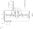
- the decimation filter 400 receives a digital input signal at an input 402 of the decimation filter 400 .
- the decimation filter 400 includes two data paths for processing the input digital stream. In a first processing path, the input digital stream is provided to a downsampler 406 , which downsamples the input digital stream by a factor of two to produce an output X 0 .
- the signal X 0 is combined with a feedback signal X 2 D through a first adder 408 producing a signal X 1 .
- Coefficient ⁇ 1 which has a value of 1 ⁇ 8 (0.125) in the illustrated embodiment, is applied to X 1 and the result is added by a second adder 410 to feedback signal X 2 D to produce output signal X 3 .
- X 3 is subtracted from X 1 by a subtractor. 412 to produce the difference signal X 2 .
- the difference signal X 2 is delayed by a factor of two samples by a delay element 414 and fed back to the first adder 408 and the second adder 410 .
- the input digital stream is fed to delay element 420 , which delays the input digital stream by one sample and is downsampled by a factor of 2 by downsampler 422 to produce an output Y 0 .
- the signal Y 0 is combined with a feedback signal Y 2 D through a third adder 424 producing signal Y 1 .
- Coefficient ⁇ 2 which has a value of 1/16 plus one half (0.5625) in the illustrated embodiment, is applied to Y 1 and the result is added by a fourth adder 426 to feedback signal Y 2 D to produce output signal Y 3 .
- Y 3 is subtracted from Y 1 by a second subtractor 430 to produce a difference signal Y 2 .
- the difference signal Y 2 is delayed two samples through a delay element 432 and fed back to the third adder 424 and the fourth adder 426 .
- the output signal X 3 from the first processing path and output signal Y 3 from the second processing path are combined by a fifth adder 450 , fed through a divider 452 and to an output 460 (OUT).
- a decimation filter 500 receives a digital input signal at an input 502 of the decimation filter 500 .
- the decimation filter 500 includes two data paths for processing the input digital stream.
- the input digital stream is provided to a downsampler 504 , which downsamples the input digital stream by a factor of two to produce a downsampled signal X 0 .
- the signal X 0 is combined with a feedback signal X 3 D through a subtractor 506 producing a signal X 1 .
- Coefficient ⁇ 1 which has a value of 1 ⁇ 8 (0.125) in the illustrated embodiment, is applied to X 1 by a component 508 to produce X 2 , which is provided to a first adder 510 .
- the downsampled signal X 0 is also provided to a delay element 514 that delays the signal by factor of two samples to produce a delayed signal X 0 D, which is combined with signal X 2 by the first adder 510 .
- the first adder 510 outputs a signal X 3 to a second adder 512 , and a copy of X 3 is fed back to the first adder 506 through a delay element 516 , which delays the signal X 3 by a factor of two samples to produce feedback signal X 3 D.
- the input digital stream is fed to delay element 520 , which delays the input digital stream by one sample, and is downsampled by a factor of two by downsampler 522 to produce an output Y 0 .
- the signal Y 0 is combined with a feedback signal Y 3 D through a second subtractor 524 producing a signal Y 1 .
- Coefficient ⁇ 2 which has a value of 1 ⁇ 8 (0.125) in the illustrated embodiment, is applied to Y 1 by a component 526 to produce Y 2 , which is provided to a third adder 528 .
- the downsampled signal Y 0 is also provided to a delay element 530 that delays the signal by factor of two samples to produce a delayed signal Y 0 D, which is combined with signal Y 2 by the third adder 528 .
- the second subtractor 524 outputs a signal Y 3 to the second adder 512 , and a copy of Y 3 is fed back to the second subtractor 524 through a delay element 532 , which delays the signal Y 3 by a factor of two samples to produce feedback signal Y 3 D.
- the output from the second adder 512 is provided to a divider 540 and then to an output 550 for further processing.
- FIGS. 6A-D illustrate examples of 13 th order lattice wave filter structures, in accordance with various embodiments of the present disclosure.
- a lattice wave filter 600 A includes three reflector stages 602 a - c on a first processing branch, and three reflector stages 602 d - f on a second processing branch.
- the stages 602 a - f may be implemented using the structures previously disclosed in FIGS. 2 and 5 .
- the output values (A) are identical allowing for the removal of delay element 610
- the output values (B) are identical allowing for the removal of delay element 612
- the output values (C) are identical allowing for the removal of delay element 614
- the output values (D) are identical allowing for the removal of delay element 616
- the output values (E) are identical, allowing for the removal of delay element 618 .
- a simplified lattice wave filter 600 C that eliminates the redundant delay elements is illustrated in FIG. 6C .
- FIG. 6D illustrates an embodiment of a simplified 13 th order lattice wave 600 D.
- the lattice wave 600 D receives an input signal 630 which is passed through two processing branches. In the first processing branch, the input signal 630 is downsampled by a factor of two by downsampler 632 , and the downsampled input signal is provided to a delay element 634 and a first subtractor 636 .
- the first subtractor 636 subtracts the feedback signal (A) received from the second stage from the downsampled input signal and produces a difference signal.
- the coefficient ⁇ 1 is multiplied by the difference signal at a component 638 and the result is combined by a first adder 640 with the delayed downsampled input signal. The resulting output is then fed to the next stage.
- the input signal 630 is delayed one sample by delay element 650 and is downsampled by a factor of two by downsampler 652 .
- the delayed and downsampled input signal is provided to a delay element 654 and a second subtractor 656 .
- the second subtractor 656 subtracts the feedback signal (C) received from the second stage from the delayed, downsampled input signal and produces a difference signal.
- the coefficient ⁇ 2 is multiplied by the difference signal at a component 658 and the result is combined by a second adder 660 with the delayed, downsampled input signal, and the resulting output is fed to the next stage. It can be seen, that the number of delay elements has been reduced from 13 to 9 delay elements when comparing the original FIG. 6A to the new 6 D. It is here assumed, that the delays are implemented using a single register operating at half the input sample rate to save register space and power.
- the low power lattice wave filters disclosed herein may be used to facilitate sample conversion in a variety of multirate systems.
- noise cancellation and noise reduction techniques are used in a variety of applications to improve user experiences in noisy environments.
- a listening device such as headphones, headsets or ear buds, includes one or more audio sensors to pick up environmental noise and adaptive noise cancellation processing circuitry to generate an anti-noise signal to cancel or reduce the environmental noise for the user. It is desirable for the generated anti-noise signal to be equal to the inverse of the noise disturbance (thereby cancelling the noise) while desired audio, such as the playback from a high-fidelity audio source, is provided with minimal disturbance.
- ANC systems are designed for low latency processing of the received noise signals to generate an inverted output signal that has a minimal phase shift with respect to the original noise signal to obtain a wide bandwidth of noise cancellation.
- the low power lattice wave filters disclosed herein are used in noise cancellation systems that use oversampled converters in high-quality audio playback systems.
- delta-sigma analog-to-digital converters (ADCs) and digital-to-analog converters (DACs) are used for audio signal processing.
- ADCs analog-to-digital converters
- DACs digital-to-analog converters
- delta-sigma converters utilize a higher sample rate and are generally cheaper to implement because they require less precision in the analog signal components. Therefore, both from a cost and processing perspective, it is often advantageous to perform the noise cancellation at a higher sample rate than required by the Nyquist criterion and this can be used to obtain a wider noise cancellation bandwidth.
- ANC systems it is desirable to provide a time-accurate reference for the active noise processing system, both of the measured noise (undesired signal) and high fidelity audio (desired signal), in order to generate an anti-noise signal that is in phase with the environmental noise to be cancelled.
- the low power lattice wave filters of the present disclosure have low sensitivity to coefficient changes and may be used to obtain low latency, even with higher filter order designs.
- FIG. 7 provides time accurate references for the ANC system while providing both a low delay path for the ANC signal and a high-fidelity signal path for the reference audio signal.
- the system 700 may be implemented in noise cancelling headphones, ear buds, mobile phones or other systems that sense noise from an environment and generate a noise cancelling signal.
- the system 700 includes at least one microphone 702 or other audio sensor to sense the environmental noise from one or more noise sources and generate corresponding electrical signals representing the sensed noise.
- the at least one microphone 702 may be arranged in a feed-forward, feedback, or combined feed forward/feed backward ANC system.
- the output of the microphone 702 may be a digital oversampled bit stream, e.g. the output from a single-bit digital microphone, or an analog signal that is provided to a preamplifier and a delta-sigma converter (single-bit or multi-bit) to produce the digital oversampled audio signal.
- the digital audio signal is decimated to a lower sample rate by a low delay decimator 704 , such as a low power multi stage lattice wave filter of the present disclosure, for input to a low delay ANC processor 706 .
- the low delay ANC processor 706 generates an anti-noise signal corresponding to the environmental noise sensed by the microphone 702 .
- the ANC processor 706 also receives a time-accurate downconverted (by 718 ), audio playback signal from the high-quality audio playback processor 708 , which is used as an audio reference signal.
- the ANC processor 706 uses a time or frequency update of internal filter nodes to adaptively filter the environmental noise from the microphone signal, which may also include desired audio played through a speaker 714 .
- the ANC processor 706 may implement a filtered-x least mean squares (FXLMS) algorithm to adaptively modify filter coefficients to filter out the environmental noise.
- FXLMS filtered-x least mean squares
- an adaptive filter topology is often used, and the filter updates may be performed in the frequency domain to obtain fast adaption even when there is a significant spread among the power spectrum of the noise. This enables fast adaptation even at frequencies where the energy content is significantly smaller than any dominant nodes by separating the signals in the frequency domain.
- An inverse frequency transform may be used to transform the adapted weights back to the time domain.
- the audio playback processor 708 generates the desired audio signal (also referred to herein as the primary audio signal) for playback through an audio output, such as speaker 714 .
- the desired audio signal may be generated from a source file (e.g., recorded music or movie file) or output from another source, such as a near end microphone or an audio signal received from a far end microphone in a voice over IP system.
- the desired audio signal is combined with the upconverted (by 720 ) anti-noise signal output by the ANC processor 706 by the adder 710 .
- the summed output of these signals is filtered using a low latency interpolator 712 and output to the speaker 714 (sometimes called a receiver).
- FIG. 7 some standard components are not shown in FIG. 7 , for example, a microphone preamplifier, a possible microphone high voltage pump used in MEMS microphones, low noise power supply unit, speaker amplifier, a power source and other components of the system 700 .
- a microphone preamplifier for example, a microphone preamplifier, a possible microphone high voltage pump used in MEMS microphones, low noise power supply unit, speaker amplifier, a power source and other components of the system 700 .
- These components are known to those skilled in the art and will be included in various practical system implementations but have been omitted here for clarity in the showing the processing path.
- both the high-fidelity audio signal and the ANC output signals are represented at the same low sample rate (e.g. 192 kHz) and are therefore both subjected to the same low-fidelity interpolation filter—provided a low latency in the processing path is a design goal. While it is possible to increase the processing sample rate, this will increase power consumption and physical size of the design considerably. Therefore, it is desired to simultaneously be able to combine a high-quality interpolation filter for audio playback and a low latency filter path for the ANC processing (also referred to herein as the adaptive noise cancellation path) as illustrated in FIG. 7 .
- the adaptive noise cancellation path also referred to herein as the adaptive noise cancellation path
- the high-quality audio playback processor 708 generates a high-quality audio signal which is fed to the high-quality interpolator 716 (i.e., a high-fidelity interpolation filter).
- the high-quality interpolator 716 i.e., a high-fidelity interpolation filter.
- this high-fidelity oversampled output of the high-quality interpolation filter is decimated by a factor of N by decimator 718 which operates without filtering (i.e., selects every Nth sample). Filtering (e.g., anti-aliasing) is not required because out-of-band signals are removed by the high-quality interpolator 716 and the signal bandwidth is therefore unchanged i.e. there is no aliasing.
- the ANC processor 706 output signal (anti-noise signal) is directly upsampled to a higher frequency in interpolator 720 by a factor of N to match the frequency of the high-quality audio signal.
- the output signal is upsampled to a higher frequency by inserting N ⁇ 1 samples equal to zero between each original sample. This operation will introduce multiple mirror aliases of the original noise signal.
- the anti-noise signal is combined with the high-fidelity oversampled output by adder 710 , and the combined output signal is sent to the low delay interpolator 712 .
- the low delay interpolator 712 in this embodiment is an oversampled interpolator that operates at the higher sample rate of the initial audio output times N and removes the aliased images that will be output from the directly interpolated signal from the ANC processor 706 , while the original oversampled high-fidelity oversampled audio signal will pass through unchanged since the aliased images have already been removed by the high-quality interpolator.
- the oversampled interpolator 712 may be implemented by adding extra delay elements inside each filter section, i.e. each filter section includes N, N/2. N/4 etc. times the original delay elements to obtain the same frequency response as the original filter configuration operating at N, N/2, N/4 times lower sample frequency.
- Example oversampled interpolator structures are described in co-pending U.S. application Ser. No. 16/177,308, filed Oct. 31, 2018, entitled LOW DELAY DECIMATOR AND INTERPOLATOR FILTERS, which is incorporated herein by reference.
- this filter configuration solves practical implementation problems, because the filter elements are updated at the much higher sample rate of N times the original sample rate, thereby enabling an optimal group delay of the filters.
- the theoretical performance may be obtained without introducing extra delays due to a practical register transfer level implementation that often can give delays when transferring values between systems with different sample rates (i.e., difference sample frequencies).
- the oversampled interpolation filter has same input and output sample frequency and can also be used as a low latency decimation filter and thereby lower latency further by reducing the input path delay. It is essentially a low pass filter with very low delay and wide bandwidth, and it is possible to add a second decimation path for high-fidelity applications.
- the filter may be optimized by first designing a filter with a response that may be ideal from an out-of-band attenuation point of view, and then further optimize the filter by adjusting the coefficients to improve the actual signal-to-noise-ratio (SNR) at the output of the filter, thereby taking the actual noise shaping of the used delta-sigma converters into account.
- the coefficients may be discretized to remove multiplications in the actual implementation thus lowering silicon area, cost and power consumption significantly.
- a digital input signal is received at an input of a multistage sample rate converter.
- the digital input signal may include any digital sampled signal, such as an audio signal in an audio processing system.
- the digital input signal is passed through a delay element in a first processing branch to produce a delayed input signal.
- a delayed feedback signal is subtracted from the digital input signal, and a filter coefficient is applied to produce a difference signal.
- the delayed input signal and the difference signal are combined to produce the feedback signal and the output signal.
- the sample rate converted output signal is output at step 810 .
- various embodiments provided by the present disclosure may be implemented using hardware, software, or combinations of hardware and software.
- the various hardware components and/or logic components set forth herein may be combined into composite components comprising software, hardware, and/or both without departing from the scope of the present disclosure.
- the various hardware components and/or logic components set forth herein may be separated into sub-components comprising software, hardware, or both without departing from the scope of the present disclosure.
- software components may be implemented as hardware components and vice versa.
Abstract
Description
Y/X=(γ+z −2)/(1+γz −2), or
Y(1+γz −2)=X(γ+z −2), which can be simplified to
Y=Xz −2+γ(X−Yz −2).
Based on this transfer function, an alternative topology is derived as illustrated in
Claims (19)
Priority Applications (2)
| Application Number | Priority Date | Filing Date | Title |
|---|---|---|---|
| US16/425,813 US10848131B1 (en) | 2019-05-29 | 2019-05-29 | Low power lattice wave filter systems and methods |
| CN202010474160.5A CN112019191A (en) | 2019-05-29 | 2020-05-29 | Low power lattice wave filter system and method |
Applications Claiming Priority (1)
| Application Number | Priority Date | Filing Date | Title |
|---|---|---|---|
| US16/425,813 US10848131B1 (en) | 2019-05-29 | 2019-05-29 | Low power lattice wave filter systems and methods |
Publications (2)
| Publication Number | Publication Date |
|---|---|
| US10848131B1 true US10848131B1 (en) | 2020-11-24 |
| US20200382104A1 US20200382104A1 (en) | 2020-12-03 |
Family
ID=73461977
Family Applications (1)
| Application Number | Title | Priority Date | Filing Date |
|---|---|---|---|
| US16/425,813 Active US10848131B1 (en) | 2019-05-29 | 2019-05-29 | Low power lattice wave filter systems and methods |
Country Status (2)
| Country | Link |
|---|---|
| US (1) | US10848131B1 (en) |
| CN (1) | CN112019191A (en) |
Citations (5)
| Publication number | Priority date | Publication date | Assignee | Title |
|---|---|---|---|---|
| US5325318A (en) * | 1992-01-31 | 1994-06-28 | Constream Corporation | Variable rate digital filter |
| US20020012389A1 (en) * | 2000-05-24 | 2002-01-31 | Jens Wildhagen | Digital filter for IQ-generation, noise shaping and neighbour channel suppression |
| US20050228840A1 (en) * | 2004-04-12 | 2005-10-13 | Benq Corporation | Lattice wave digital filter |
| US20080240467A1 (en) * | 2007-03-09 | 2008-10-02 | Srs Labs, Inc. | Frequency-warped audio equalizer |
| US8521798B2 (en) * | 2008-09-22 | 2013-08-27 | Magor Communications Corporation | Second order real allpass filter |
-
2019
- 2019-05-29 US US16/425,813 patent/US10848131B1/en active Active
-
2020
- 2020-05-29 CN CN202010474160.5A patent/CN112019191A/en active Pending
Patent Citations (5)
| Publication number | Priority date | Publication date | Assignee | Title |
|---|---|---|---|---|
| US5325318A (en) * | 1992-01-31 | 1994-06-28 | Constream Corporation | Variable rate digital filter |
| US20020012389A1 (en) * | 2000-05-24 | 2002-01-31 | Jens Wildhagen | Digital filter for IQ-generation, noise shaping and neighbour channel suppression |
| US20050228840A1 (en) * | 2004-04-12 | 2005-10-13 | Benq Corporation | Lattice wave digital filter |
| US20080240467A1 (en) * | 2007-03-09 | 2008-10-02 | Srs Labs, Inc. | Frequency-warped audio equalizer |
| US8521798B2 (en) * | 2008-09-22 | 2013-08-27 | Magor Communications Corporation | Second order real allpass filter |
Also Published As
| Publication number | Publication date |
|---|---|
| CN112019191A (en) | 2020-12-01 |
| US20200382104A1 (en) | 2020-12-03 |
Similar Documents
| Publication | Publication Date | Title |
|---|---|---|
| US8611551B1 (en) | Low latency active noise cancellation system | |
| US11205412B1 (en) | Hybrid active noise cancellation filter adaptation | |
| US9407236B2 (en) | System and method for processing a signal with a filter employing FIR and IIR elements | |
| US8848935B1 (en) | Low latency active noise cancellation system | |
| US8953813B2 (en) | Reduced delay digital active noise cancellation | |
| US10115386B2 (en) | Delay techniques in active noise cancellation circuits or other circuits that perform filtering of decimated coefficients | |
| JP4979809B2 (en) | Low delay signal processing based on high oversampling digital processing | |
| US11189261B1 (en) | Hybrid active noise control system | |
| US10904661B2 (en) | Low delay decimator and interpolator filters | |
| US11107453B2 (en) | Anti-noise signal generator | |
| US20190027126A1 (en) | Active noise cancellation system | |
| JP4372184B2 (en) | Sample rate converter | |
| US10848131B1 (en) | Low power lattice wave filter systems and methods | |
| US9082392B2 (en) | Method and apparatus for a configurable active noise canceller | |
| US10755721B1 (en) | Multichannel, multirate, lattice wave filter systems and methods | |
| US11329634B1 (en) | Digital filter structure | |
| US20240054988A1 (en) | Reduced Complexity Implementation for Acoustic Noise Canceling |
Legal Events
| Date | Code | Title | Description |
|---|---|---|---|
| FEPP | Fee payment procedure |
Free format text: ENTITY STATUS SET TO UNDISCOUNTED (ORIGINAL EVENT CODE: BIG.); ENTITY STATUS OF PATENT OWNER: LARGE ENTITY |
|
| AS | Assignment |
Owner name: SYNAPTICS INCORPORATED, CALIFORNIA Free format text: ASSIGNMENT OF ASSIGNORS INTEREST;ASSIGNORS:LI, JACKY;POULSEN, JENS KRISTIAN;HARIHARAN, HARI;SIGNING DATES FROM 20190424 TO 20190430;REEL/FRAME:050251/0376 |
|
| AS | Assignment |
Owner name: WELLS FARGO BANK, NATIONAL ASSOCIATION, NORTH CAROLINA Free format text: SECURITY INTEREST;ASSIGNOR:SYNAPTICS INCORPORATED;REEL/FRAME:051936/0103 Effective date: 20200214 |
|
| STCF | Information on status: patent grant |
Free format text: PATENTED CASE |
|
| AS | Assignment |
Owner name: SYNAPTICS INCORPORATED, CALIFORNIA Free format text: RELEASE BY SECURED PARTY;ASSIGNOR:WELLS FARGO BANK, NATIONAL ASSOCIATION;REEL/FRAME:055561/0083 Effective date: 20201217 |
|
| AS | Assignment |
Owner name: GOOGLE LLC, CALIFORNIA Free format text: ASSIGNMENT OF ASSIGNORS INTEREST;ASSIGNOR:SYNAPTICS INCORPORATED;REEL/FRAME:055576/0502 Effective date: 20201216 |