US10840381B2 - Nanosheet and nanowire MOSFET with sharp source/drain junction - Google Patents
Nanosheet and nanowire MOSFET with sharp source/drain junction Download PDFInfo
- Publication number
- US10840381B2 US10840381B2 US15/233,386 US201615233386A US10840381B2 US 10840381 B2 US10840381 B2 US 10840381B2 US 201615233386 A US201615233386 A US 201615233386A US 10840381 B2 US10840381 B2 US 10840381B2
- Authority
- US
- United States
- Prior art keywords
- stack
- forming
- type
- semiconductor materials
- semiconductor
- Prior art date
- Legal status (The legal status is an assumption and is not a legal conclusion. Google has not performed a legal analysis and makes no representation as to the accuracy of the status listed.)
- Expired - Fee Related, expires
Links
Images


Classifications
-
- H01L29/78696—
-
- H—ELECTRICITY
- H10—SEMICONDUCTOR DEVICES; ELECTRIC SOLID-STATE DEVICES NOT OTHERWISE PROVIDED FOR
- H10D—INORGANIC ELECTRIC SEMICONDUCTOR DEVICES
- H10D30/00—Field-effect transistors [FET]
- H10D30/60—Insulated-gate field-effect transistors [IGFET]
- H10D30/67—Thin-film transistors [TFT]
- H10D30/6757—Thin-film transistors [TFT] characterised by the structure of the channel, e.g. transverse or longitudinal shape or doping profile
-
- H01L21/2255—
-
- H01L29/0673—
-
- H01L29/42392—
-
- H01L29/66439—
-
- H01L29/66545—
-
- H—ELECTRICITY
- H10—SEMICONDUCTOR DEVICES; ELECTRIC SOLID-STATE DEVICES NOT OTHERWISE PROVIDED FOR
- H10D—INORGANIC ELECTRIC SEMICONDUCTOR DEVICES
- H10D30/00—Field-effect transistors [FET]
- H10D30/01—Manufacture or treatment
- H10D30/014—Manufacture or treatment of FETs having zero-dimensional [0D] or one-dimensional [1D] channels, e.g. quantum wire FETs, single-electron transistors [SET] or Coulomb blockade transistors
-
- H—ELECTRICITY
- H10—SEMICONDUCTOR DEVICES; ELECTRIC SOLID-STATE DEVICES NOT OTHERWISE PROVIDED FOR
- H10D—INORGANIC ELECTRIC SEMICONDUCTOR DEVICES
- H10D30/00—Field-effect transistors [FET]
- H10D30/60—Insulated-gate field-effect transistors [IGFET]
- H10D30/67—Thin-film transistors [TFT]
- H10D30/6729—Thin-film transistors [TFT] characterised by the electrodes
- H10D30/673—Thin-film transistors [TFT] characterised by the electrodes characterised by the shapes, relative sizes or dispositions of the gate electrodes
- H10D30/6735—Thin-film transistors [TFT] characterised by the electrodes characterised by the shapes, relative sizes or dispositions of the gate electrodes having gates fully surrounding the channels, e.g. gate-all-around
-
- H—ELECTRICITY
- H10—SEMICONDUCTOR DEVICES; ELECTRIC SOLID-STATE DEVICES NOT OTHERWISE PROVIDED FOR
- H10D—INORGANIC ELECTRIC SEMICONDUCTOR DEVICES
- H10D62/00—Semiconductor bodies, or regions thereof, of devices having potential barriers
- H10D62/10—Shapes, relative sizes or dispositions of the regions of the semiconductor bodies; Shapes of the semiconductor bodies
- H10D62/117—Shapes of semiconductor bodies
- H10D62/118—Nanostructure semiconductor bodies
- H10D62/119—Nanowire, nanosheet or nanotube semiconductor bodies
- H10D62/121—Nanowire, nanosheet or nanotube semiconductor bodies oriented parallel to substrates
-
- H—ELECTRICITY
- H10—SEMICONDUCTOR DEVICES; ELECTRIC SOLID-STATE DEVICES NOT OTHERWISE PROVIDED FOR
- H10D—INORGANIC ELECTRIC SEMICONDUCTOR DEVICES
- H10D64/00—Electrodes of devices having potential barriers
- H10D64/01—Manufacture or treatment
- H10D64/017—Manufacture or treatment using dummy gates in processes wherein at least parts of the final gates are self-aligned to the dummy gates, i.e. replacement gate processes
-
- H—ELECTRICITY
- H10—SEMICONDUCTOR DEVICES; ELECTRIC SOLID-STATE DEVICES NOT OTHERWISE PROVIDED FOR
- H10P—GENERIC PROCESSES OR APPARATUS FOR THE MANUFACTURE OR TREATMENT OF DEVICES COVERED BY CLASS H10
- H10P32/00—Diffusion of dopants within, into or out of wafers, substrates or parts of devices
- H10P32/10—Diffusion of dopants within, into or out of semiconductor bodies or layers
- H10P32/14—Diffusion of dopants within, into or out of semiconductor bodies or layers within a single semiconductor body or layer in a solid phase; between different semiconductor bodies or layers, both in a solid phase
- H10P32/1408—Diffusion of dopants within, into or out of semiconductor bodies or layers within a single semiconductor body or layer in a solid phase; between different semiconductor bodies or layers, both in a solid phase from or through or into an external applied layer, e.g. photoresist or nitride layers
- H10P32/141—Diffusion of dopants within, into or out of semiconductor bodies or layers within a single semiconductor body or layer in a solid phase; between different semiconductor bodies or layers, both in a solid phase from or through or into an external applied layer, e.g. photoresist or nitride layers the applied layer comprising oxides only
-
- H—ELECTRICITY
- H10—SEMICONDUCTOR DEVICES; ELECTRIC SOLID-STATE DEVICES NOT OTHERWISE PROVIDED FOR
- H10P—GENERIC PROCESSES OR APPARATUS FOR THE MANUFACTURE OR TREATMENT OF DEVICES COVERED BY CLASS H10
- H10P32/00—Diffusion of dopants within, into or out of wafers, substrates or parts of devices
- H10P32/10—Diffusion of dopants within, into or out of semiconductor bodies or layers
- H10P32/17—Diffusion of dopants within, into or out of semiconductor bodies or layers characterised by the semiconductor material
- H10P32/171—Diffusion of dopants within, into or out of semiconductor bodies or layers characterised by the semiconductor material being group IV material
Definitions
- the present disclosure relates to semiconductor devices, and more particularly to semiconductor devices including channel regions integrated within nanowires and nano-sheets.
- CMOS complementary metal oxide semiconductor
- the present disclosure provides a suspended channel field effect transistor (FET).
- the suspended channel field effect transistor may include a gate structure present on at least two suspended channel structures; and a composite spacer present on sidewalls of the gate structure.
- the composite spacer may include a cladding spacer present along a cap portion of the gate structure, and an inner spacer along the channel portion of the gate structure between adjacent channel semiconductor layers of said at least two suspended channel structures.
- the inner spacer may include an n-type or p-type doped glass.
- a method of forming a suspended channel field effect transistor includes forming a gate structure on a stack of at least two semiconductor materials, wherein a spacer is present on sidewalls of the gate structure, and etching exposed portions of the stack of at least two semiconductor materials with an etch process.
- the etch process includes a stage that removes one of the at least two semiconductor materials at a faster rate than a second of the at least two semiconductor materials to provide a divot region undercutting the spacer.
- An n-type or p-type doped glass is formed that fills the divot region.
- Epitaxial semiconductor material is formed on remaining semiconductor material from said stack of at least two semiconductor materials.
- the present disclosure provides a method of forming a semiconductor device that may include forming a replacement gate structure on a channel portion of a stack of at least two semiconductor materials.
- a cladding spacer may be formed on sidewalls of the replacement gate structure.
- a first etch process is applied to remove one of the at least two semiconductor materials to provide a divot region undercutting the spacer.
- An n-type or p-type doped glass layer is formed on sidewalls of the channel opening, wherein the n-type or p-type doped glass layer fills the divot.
- the replacement gate structure may be removed to provide a gate opening that exposes a channel portion of the stack of the two semiconductor materials.
- a second etch process is applied to remove one of the at least two semiconductor materials the channel portion of the at least two semiconductor materials to provide a plurality of suspended channels.
- a functional gate structure is formed in the channel opening.
- FIG. 1 is a perspective view depicting one embodiment of forming a replacement gate structure on a fin structure stack of at least two semiconductor materials, wherein a cladding spacer is present on sidewalls of the replacement gate structure, in accordance with one embodiment of the present disclosure.
- FIG. 2A is a side cross-sectional view along the source to drain direction of FIG. 1 .
- FIG. 2B is a side cross-sectional view through the spacer of FIG. 2A .
- FIG. 3 is a side cross-sectional view along the side cross-section of the fin structure stack along the source to drain direction illustrating one embodiment of removing exposed portions of the fin structure stack that extend beyond the outer sidewall of the cladding spacer.
- FIG. 4A is a side cross-sectional view along the side cross-section of the fin structure stack along the source to drain direction illustrating one embodiment of applying a first etch process to remove one of the at least two semiconductor materials of the fin structure stack to form a divot regions undercutting the cladding spacer, in accordance with one embodiment of the present disclosure.
- FIG. 4B is a cross-sectional view through the spacer illustrating the formation of a void, i.e., divot region, which is undercutting the cladding spacer.
- FIG. 5A is a side cross-sectional view along the side cross-section of the fin structure stack along the source to drain direction depicting forming an n-type or p-type doped glass layer on etched sidewalls of the fin structure stack to fill the divot regions, in accordance with one embodiment of the present disclosure.
- FIG. 5B is a cross-sectional view through the spacer illustrating the void, i.e., divot region, that is undercutting the cladding spacer being filled with the n-type or p-type doped glass layer.
- FIG. 6 is a side cross-sectional view along the side cross-section of the fin structure stack along the source to drain direction depicting forming epitaxial semiconductor material on source and drain portions of the stack of the at least two semiconductor materials.
- FIG. 7 is a side cross-sectional view of the fin structure stack along the source to drain direction depicting one embodiment of removing the replacement gate structure to provide a gate opening, and applying a second etch process to remove one of the at least two semiconductor materials from the channel portion of the at least two semiconductor materials to provide a plurality of suspended channels, in accordance with one embodiment of the present disclosure.
- FIG. 8A is a side cross-sectional view of the fin structure stack along the source to drain direction of forming a second replacement gate structure in the gate opening, and applying a drive in anneal to drive dopants from the n-type or p-type doped glass into the junction with the suspended channels.
- FIG. 8B is a cross-sectional view through the spacer illustrating the portions of the suspended channel underlying the cladding spacer being doped with the n-type or p-type dopant that has been driven from the n-type or p-type doped glass by the drive in anneal.
- FIG. 9 is a side cross-sectional view of the fin structure stack along the source to drain direction depicting substituting the second replacement gate structure with a functional gate structure, in accordance with one embodiment of the present disclosure.
- FIG. 10 is a side cross-sectional view of the fin structure stack along the source to drain direction depicting one embodiment of forming contacts to the source and drain regions of the device.
- first element such as a first structure
- second element such as a second structure
- intervening elements such as an interface structure, e.g. interface layer
- directly contact means that a first element, such as a first structure, and a second element, such as a second structure, are connected without any intermediary conducting, insulating or semiconductor layers at the interface of the two elements.
- Nanosheet (nanowire) MOSFET is a candidate for future CMOS technology.
- Nanowire and/or nanowire MOSFETs can provide better gate electrostatic control and larger effective device width per footprint (multiple nanosheets in one stack).
- an inner spacer between nanosheets can reduce the parasitic capacitance between a gate to the nanosheets and the source/drain region.
- the nanosheets typically have high doping at the spacer region, e.g., 5 ⁇ 10 18 dopants/cm 3 to 1 ⁇ 10 19 dopants/cm 3 .
- the methods and structures disclosed herein provide a nanosheet metal oxide semiconductor field effect transistor (MOSFET) structure with an inner spacer composed of boron/phosphorus doped glass, e.g., boron doped silicate glass or phosphorus doped silicate glass, which helps to provide a high dopant concentration in the spacer region, without introducing too many dopants in the channel region.
- MOSFET nanosheet metal oxide semiconductor field effect transistor
- the inner spacer that is composed boron/phosphorus doped glass e.g., boron doped silicate glass or phosphorus doped silicate glass, facilitates the formation of an abrupt junction, i.e., sharp source/drain junction (sharp S/D junction). Further details regarding the method and structures of the present disclosure are now described with reference to FIGS. 1-10 .
- FIG. 1 depicts one embodiment of forming a first replacement gate structure 15 on a stack 10 of at least two semiconductor materials 5 a , 5 b that can be etched selectively to one another, wherein a cladding spacer 20 is present on sidewalls of the gate structure 15 .
- the stack 10 of the at least two semiconductor materials 5 a , 5 b may be present on a substrate 1 .
- the substrate 1 may be composed of a supporting material, such as a semiconductor material, e.g., silicon, or dielectric material, such as silicon oxide or silicon nitride.
- the stack 10 of the at least two semiconductor materials 5 a , 5 b is typically composed of two alternating materials.
- the first semiconductor material 5 a that is present on the substrate 1 may be composed of a silicon and germanium containing semiconductor material, such as silicon germanium (SiGe), whereas the second semiconductor material 5 b that is present on the first semiconductor material 5 b may be composed of a germanium free silicon containing semiconductor material, such as silicon (Si). It is noted that this is only one example of semiconductor materials that may be used for the at least two semiconductor materials 5 a , 5 b .
- any semiconductor material composition may be used for each of the at least two semiconductor materials 5 a , 5 b so long as at least one of the compositions selected allow for selective etching between at least two of them.
- Any type IV semiconductor composition combination and/or III-V semiconductor composition combination is suitable for use with the present disclosure.
- the compositions selected for the at least two semiconductor materials include Si, SiGe, SiGeC, SiC, single crystal Si, polysilicon, i.e., polySi, epitaxial silicon, i.e., epi-Si, amorphous Si, i.e., ⁇ :Si, germanium, gallium arsenide, gallium nitride, cadmium telluride and zinc sellenide.
- FIG. 1 only depicts two semiconductor material layers in the stack 10 of the at least two semiconductor materials 5 a , 5 b , it is noted that the present disclosure is not limited to only this example. Any number of semiconductor material layers 5 a , 5 b may be present in the stack 10 .
- the number of semiconductor material layers 5 a , 5 b in the stack may also be equal to 3, 4, 5, 10, 15 and 20, as well as any value between the aforementioned examples.
- the first semiconductor material 5 a is silicon germanium (SiGe)
- the second semiconductor material 5 b is silicon (Si).
- the stack 10 of the at least two semiconductor materials 5 a , 5 b may be formed using a deposition process, such as chemical vapor deposition (CVD).
- Chemical vapor deposition (CVD) is a deposition process in which a deposited species is formed as a result of chemical reaction between gaseous reactants at greater than room temperature (25° C. to 900° C.); wherein solid product of the reaction is deposited on the surface on which a film, coating, or layer of the solid product is to be formed.
- CVD processes suitable for use the present disclosure include, but not limited to, Atmospheric Pressure CVD (APCVD), Low Pressure CVD (LPCVD) and Plasma Enhanced CVD (PECVD), Metal-Organic CVD (MOCVD) and combinations thereof may also be employed.
- APCVD Atmospheric Pressure CVD
- LPCVD Low Pressure CVD
- PECVD Plasma Enhanced CVD
- MOCVD Metal-Organic CVD
- each of the at least two semiconductor material layers 5 a , 5 b may range from 1 nm to 30 nm. In another embodiment, the thickness of each of the at least two semiconductor material layers 5 a , 5 b , may range from 5 nm to 20 nm.
- the semiconductor material layers 5 a , 5 b may be patterned to provide the geometry of the stack.
- the semiconductor material layers 5 a , 5 b may be patterned using deposition, photolithography and subtractive etch processing.
- the stack 10 may have a height H 1 ranging from 5 nm to 200 nm, and a width ranging from 5 nm to 60 nm.
- the stack of the semiconductor material layers 5 a , 5 b may be referred to as a fin stack.
- the process flow may continue with forming a first replacement gate structure 15 on a channel portion of the stack 10 of the at least two semiconductor materials 5 a , 5 b .
- replacement it is meant that the structure is present during processing of the semiconductor device, but is removed from the semiconductor device prior to the device being completed.
- a replacement gate structure 15 is employed as part of a replacement gate process.
- replacement gate structure denotes a sacrificial structure that dictates the geometry and location of the later formed functioning gate structure.
- the “functional gate structure” operates to switch the semiconductor device from an “on” to “off” state, and vice versa.
- the sacrificial material that provides the replacement gate structure 15 may be composed of any material that can be etched selectively to the at least one of the material layers of the stack 10 of the at least two semiconductor materials 5 a , 5 b .
- the replacement gate structure 15 may be composed of a silicon-including material, such as polysilicon.
- the replacement gate structure 15 may be composed of a dielectric material, such as an oxide, nitride or oxynitride material, or amorphous carbon.
- the replacement gate structure 15 may be formed using deposition (e.g., chemical vapor deposition) photolithography and etch processes (e.g., reactive ion etching).
- a cladding spacer 20 is formed on the sidewall of the replacement gate structure 15 .
- the cladding spacer 20 is typically composed of a dielectric material, such as an oxide, nitride, or oxynitride material.
- the cladding spacer 20 may be composed of silicon nitride
- the spacer 20 is composed of oxide
- the cladding spacer 20 may be composed of silicon oxide.
- the cladding spacer 20 may be composed of a low-k dielectric.
- the low-k dielectric of the cladding spacer 20 may have a dielectric constant of 4.0 or less (measured at room temperature, e.g., 25° C., and 1 atm).
- a low-k dielectric material suitable for the spacer 20 may have a dielectric constant ranging from about 1.0 to about 3.0.
- low-k materials suitable for the cladding spacer 20 include organosilicate glass (OSG), fluorine doped silicon dioxide, carbon doped silicon dioxide, porous silicon dioxide, porous carbon doped silicon dioxide, spin-on organic polymeric dielectrics (e.g., SILKTM), spin-on silicone based polymeric dielectric (e.g., hydrogen silsesquioxane (HSQ) and methylsilsesquioxane (MSQ), and combinations thereof.
- organosilicate glass fluorine doped silicon dioxide
- carbon doped silicon dioxide e.g., porous silicon dioxide, porous carbon doped silicon dioxide
- spin-on organic polymeric dielectrics e.g., SILKTM
- spin-on silicone based polymeric dielectric e.g., hydrogen silsesquioxane (HSQ) and methylsilsesquioxane (MSQ)
- the cladding spacer 20 may be formed using a deposition process, such as chemical vapor deposition (CVD), and an anisotropic etchback method.
- the cladding spacer 20 may be present on the sidewalls of the replacement gate structure 15 , and may have a thickness T 1 ranging from 1 nm to 15 nm.
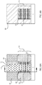
- FIG. 2A is a side cross-sectional view along section line A-A of FIG. 1 .
- This cross-section when referring to the figures disclosed herein, i.e., FIGS. 3, 4A, 5A, 6, 7, 8A, 9 and 10 , is hereafter referred to as a side cross-section of a fin structure stack 10 along source to drain direction.
- FIG. 2B is a side cross-sectional view along section line B-B of the structure depicted in FIG. 1 .
- This cross-section when referring to the figure disclosed herein, i.e., FIGS. 4B, 5B and 8B is hereafter referred to as through the spacer, i.e., cladding spacer 20 .
- FIG. 3 depicts etching the exposed portions of the stack 10 of two semiconductor materials 5 a , 5 b that extend beyond the outer sidewall of the cladding spacer 20 .
- the etch process for removing the exposed portions of the stack 10 of the at least two semiconductor materials 5 a , 5 b is an anisotropic etch process.
- anisotropic etch process denotes a material removal process in which the etch rate in the direction normal to the surface to be etched is greater than in the direction parallel to the surface to be etched.
- the anisotropic etch may include reactive-ion etching (RIE).
- anisotropic etching that can be used at this point of the present disclosure include ion beam etching, plasma etching or laser ablation.
- the etch process for etching the stack 10 is a timed etch. In the embodiment that is depicted in FIG. 3 , the etch process may continue until the entirety of the portions of the stack 10 that extend beyond the outer sidewall of the cladding spacer 20 are removed.
- the etch process for removing the portion of the stack 10 that extends beyond the outer sidewall of the spacer 20 may be a selective etch process.
- the term “selective” in reference to a material removal process denotes that the rate of material removal for a first material is greater than the rate of removal for at least another material of the structure to which the material removal process is being applied.
- a selective etch may include an etch chemistry that removes a first material selectively to a second material by a ratio of 10:1 or greater, e.g., 1000:1.
- the etch process may remove the exposed silicon and germanium containing material of the first semiconductor layer 5 a , e.g., silicon germanium (SiGe), and the exposed silicon material that is free of germanium in the second semiconductor layer 5 b , selectively to at least one of the silicon nitride material of the spacer 20 , the replacement gate structure 15 and the substrate 1 .
- an etch block mask such as a photoresist or hardmask, e.g., silicon nitride mask, may be formed over the replacement gate structure 15 during the etch process for removing the exposed portions of the stack 10 of the at least first and second semiconductor material 5 a , 5 b.
- FIGS. 4A and 4B depict applying an etch process to remove one of the at least two semiconductor materials 5 a , 5 b of the fin structure stack 10 to form a divot regions 25 undercutting the cladding spacer 20 .
- FIG. 4B illustrates the formation of a void, i.e., divot region 25 , that is undercutting the cladding spacer 20 .
- the etch process for forming the divot 25 is isotropic. By isotropic it is meant that the etch process is non-directional.
- the etch for forming the divot 25 may be referred to as an undercut etch or a lateral etch.
- an isotropic etch such as a plasma etch or wet chemical etch, may remove a portion of one of the first and second semiconductor layers 5 a , 5 b of the stack 10 selectively to at least one of the other semiconductor material layers of the stack 10 .
- a plasma etch or wet chemical etch may remove a portion of one of the first and second semiconductor layers 5 a , 5 b of the stack 10 selectively to at least one of the other semiconductor material layers of the stack 10 .
- the etch chemistry of the second stage of the first etch process may be selected to remove silicon germanium without substantially etching the silicon.
- the isotropic nature of the etch process produces a divot region 35 in underlying the cladding spacer 20 by removing the first semiconductor layer 5 a etching inward from the exposed sidewall of the stack 10 that is substantially aligned with the outside sidewall of the cladding spacer 20 selectively to the second semiconductor layer 5 b . It is noted that removing the first semiconductor layer 5 a selectively to the second semiconductor layer 5 b is only one example of the present disclosure, and the etch selectivity with respect to the first and second semiconductor layers 5 a , 5 b and the isotropic etch may be reversed.
- the second etch stage i.e., isotropic etch
- the second etch stage may be continued until a divot region 25 is formed undercutting the spacer 20 that has a dimension D 1 ranging from 1 nm to 20 nm.
- the lateral etch step may be continued until a divot region 25 is formed undercutting the spacer 20 that has a dimension D 1 ranging from 1 nm to 10 nm.
- FIG. 4B illustrates the void that provides the divot region 25 .
- FIGS. 5A and 5B depicts forming an n-type or p-type doped glass layer 30 on etched sidewalls of the fin structure stack to fill the divot regions 25 .
- FIG. 5B is a cross-sectional view through the cladding spacer 20 illustrating the void, i.e., divot region 25 , that is undercutting the cladding spacer 20 being filled with the n-type or p-type doped glass layer 30 .
- p-type refers to the addition of impurities to an intrinsic semiconductor that creates deficiencies of valence electrons.
- examples of p-type dopants include but are not limited to: boron, aluminum, gallium and indium.
- n-type refers to the addition of impurities that contributes free electrons to an intrinsic semiconductor.
- examples of n-type dopants, i.e., impurities include but are not limited to antimony, arsenic and phosphorous.
- the n-type or p-type doped glass layer 30 may be silicate glass doped with a p-type dopant, such as boron.
- the p-type doped glass layer may include boron doped silicate glass (BSG). It is noted that the above example is provided for illustrative purposes only and is not intended to limit the present disclosure, as other p-type dopants may be integrated into the p-type doped glass.
- the n-type or p-type doped glass layer 30 may be doped with an n-type dopant, such as arsenic.
- the n-type doped glass layer 30 may include phosphosilicate glass (PSG) (n-type silicate glass) and arsenosilicate glass (ASG) (n-type silicate glass).
- PSG phosphosilicate glass
- ASG arsenosilicate glass
- the above example is provided for illustrative purposes only and is not intended to limit the present disclosure, as other n-type dopants and/or p-type dopants may be integrated into the n-type or p-type doped glass layer 30 .
- the n-type or p-type doped glass layer 30 may be deposited by atomic layer deposition (ALD).
- ALD Atomic Layer Deposition
- CVD chemical vapor deposition
- ALD uses self-limiting surface reactions to deposit material layers in the monolayer or sub-monolayer thickness regime.
- ALD is similar in chemistry to chemical vapor deposition (CVD), except that the ALD reaction breaks the CVD reaction into two half-reactions, keeping the precursor materials separate during the reaction.
- the atomic layer deposition (ALD) process may be a thin film deposition method in which a film is grown on a deposition surface by exposing the surface to alternate gaseous species (typically referred to as precursors).
- the precursors are never present simultaneously in the reactor, but they are inserted as a series of sequential, non-overlapping pulses. In each of these pulses, the precursor molecules react with the surface in a self-limiting way, so that the reaction terminates once all the reactive sites on the surface are consumed.
- the monolayer deposition provided by the atomic layer depositions mechanisms provides that the layer be conformal.
- the atomic layer deposition (ALD) process may be continued until at least the entirety of the divot regions 25 are filled.
- the ALD process may continue until the entirety of the divot regions 25 are filled, in which a portion of the deposited layer of the n-type or p-type doped glass extends onto the exposed sidewall portions of the stack 10 outside the divot region 25 .
- the n-type or p-type doped glass layer 30 may be deposited using chemical vapor deposition (CVD), such as plasma enhanced CVD (PECVD) or metal organic chemical vapor deposition (MOCVD).
- CVD chemical vapor deposition
- PECVD plasma enhanced CVD
- MOCVD metal organic chemical vapor deposition
- the n-type or p-type doped glass layer 30 may also be formed using chemical solution deposition or spin on deposition, e.g., spin on glass deposition.
- the dopant may be introduced to the doped glass layer in-situ.
- in-situ it is meant that the dopant e.g., n-type or p-type, that is being introduced to the n-type or p-type doped glass layer 30 is introduced during the deposition step that forms the n-type or p-type doped glass layer 30 .
- the thickness of the n-type or p-type doped glass layer 30 may range from 2 nm to 50 nm. In other embodiments, the thickness of the n-type or p-type doped glass layer 30 ranges from 5 nm to 25 nm.
- FIGS. 5A and 5B depict a second etch process that removes any portion of the n-type or p-type doped glass layer 30 that is extending from the divot 25 and exposes sidewalls of the remaining portion of the stack 10 .
- the second etch process may include an isotropic etch, such as a plasma etch or wet chemical etch, that removes the atomic layer (ALD) deposited n-type or p-type doped glass layer 30 from the sidewalls of the stack 10 , as well as any portion of the n-type or p-type doped glass layer 30 that extends onto the upper surface of the first replacement gate structure 15 , the cladding spacer 20 and the upper surface of the substrate 1 .
- ALD atomic layer
- the second etch may form a curvature in the atomic layer deposited (ALD) n-type or p-type doped glass layer 30 that is present in the divot region 25 .
- the curvature undercuts the outside sidewall of the spacer 20 with the apex of the curvature within the divot region 25 .
- FIG. 5B illustrates the void of the divot region 25 being filled with the material of the n-type or p-type doped glass layer 30 .
- FIG. 6 depicts one embodiment of forming epitaxial semiconductor material 35 on the exposed sidewalls of the remaining portion of the stack 10 of the two semiconductor materials 5 a , 5 b .
- the epitaxial semiconductor material 35 may provide at least a portion of the source and drain regions of the semiconductor device.
- the term “epitaxial semiconductor material” denotes a semiconductor material that has been formed using an epitaxial deposition or growth process. “Epitaxial growth and/or deposition” means the growth of a semiconductor material on a deposition surface of a semiconductor material, in which the semiconductor material being grown has substantially the same crystalline characteristics as the semiconductor material of the deposition surface.
- the depositing atoms arrive at the deposition surface with sufficient energy to move around on the surface and orient themselves to the crystal arrangement of the atoms of the deposition surface.
- an epitaxial film deposited on a ⁇ 100 ⁇ crystal surface will take on a ⁇ 100 ⁇ orientation.
- drain means a doped region in semiconductor device located at the end of the channel region, in which carriers are flowing out of the transistor through the drain.
- source is a doped region in the semiconductor device, in which majority carriers are flowing into the channel region.
- the epitaxial semiconductor material 35 grows from the etched sidewall surface of the second semiconductor layer 5 b .
- the epitaxial semiconductor material 35 may be composed of silicon (Si), germanium (Ge), silicon germanium (SiGe), silicon doped with carbon (Si:C) or the epitaxial semiconductor material 35 may be composed of a type III-V compound semiconductor, such as gallium arsenide (GaAs).
- a number of different sources may be used for the epitaxial deposition of the epitaxial semiconductor material 35 .
- silicon including source gasses may include silane, disilane, trisilane, tetrasilane, hexachlorodisilane, tetrachlorosilane, dichlorosilane, trichlorosilane, methylsilane, dimethylsilane, ethylsilane, methyldisilane, dimethyldisilane, hexamethyldisilane and combinations thereof.
- germanium including source gasses for epitaxially forming an undoped epitaxial semiconductor material 6 a , 6 b of a germanium containing semiconductor examples include germane, digermane, halogermane, dichlorogermane, trichlorogermane, tetrachlorogermane and combinations thereof.
- Epitaxial deposition may be carried out in a chemical vapor deposition apparatus, such as a metal organic chemical vapor deposition (MOCVD) apparatus or a plasma enhanced chemical vapor deposition (PECVD) apparatus.
- the epitaxial semiconductor material 35 may be in situ doped to a p-type or n-type conductivity.
- the term “in situ” denotes that a dopant, e.g., n-type or p-type dopant, is introduced to the base semiconductor material, e.g., silicon or silicon germanium, during the formation of the base material.
- an in situ doped epitaxial semiconductor material may introduce n-type or p-type dopants to the material being formed during the epitaxial deposition process that includes n-type or p-type source gasses.
- the doped epitaxial semiconductor material 35 is doped with a p-type dopant to have a p-type conductivity.
- examples of p-type dopants, i.e., impurities include but are not limited to, boron, aluminum, gallium and indium.
- examples of n-type dopants, i.e., impurities include but are not limited to antimony, arsenic and phosphorous.
- Alkylphosphines include trimethylphosphine ((CH 3 ) 3 P), dimethylphosphine ((CH 3 ) 2 PH), triethylphosphine ((CH 3 CH 2 ) 3 P) and diethylphosphine ((CH 3 CH 2 ) 2 PH).
- the p-type gas dopant source may include diborane (B 2 H 6 ).
- the conductivity type of the epitaxial semiconductor region 35 i.e., whether the epitaxial semiconductor region 35 has an n-type or p-type conductivity, is typically the same as the conductivity type of the n-type or p-type glass layer 30 that is present within the divot region 25 .
- the dopant for the epitaxial semiconductor material 35 that dictates the conductivity type of the source and drain regions is typically present in a concentration ranging from 1E17 atoms/cm 3 to 5E19 atoms/cm 3 .
- FIG. 7 depicts removing a first replacement gate structure 15 and removing one of the two semiconductor materials, e.g., the first semiconductor material layer 5 a , of the stack in a channel region of the device.
- removing the replacement gate structure 15 may begin with forming an interlevel dielectric layer 40 on the structure depicted in FIG. 6 , and planarizing the interlevel dielectric layer 40 to expose an upper surface of the replacement gate structure 15 .
- the replacement gate structure 15 may be removed using a wet or dry etch process.
- the first replacement gate structure 15 may be removed by at least one of an anisotropic etch process, such as reactive ion etch (RIE), or an isotropic etch process, such as a wet chemical etch.
- the etch process for removing the first replacement gate structure 15 can include an etch chemistry for removing the first replacement gate structure 15 is selective to the material layers of the stack 10 of the first and second semiconductor material layers 5 a , 5 b.
- At least one of the material layers of the stack 10 is removed selectively to at least a remaining material composition that provides suspended channel structures 50 .
- the first semiconductor material layer 5 a is composed of silicon germanium (SiGe) and the second semiconductor material layer 5 b is composed of silicon
- the first semiconductor material layer 5 a may be removed selectively to the second semiconductor material layer 5 b with an etch process, such as a wet chemical etch. Removing the replacement gate structure 15 produces a gate opening 45 that exposes a channel portion of the stack 10 of the two semiconductor materials 5 a , 5 b.
- a suspended channel structure 50 is provided following removal of one of the material layers of the stack 10 , e.g., removal of the first semiconductor material layer 5 a of the stack 10 .
- suspended channel it is meant that at least one semiconductor material layer is present overlying the substrate 1 , wherein the sidewalls of the suspended channel 50 are supported, e.g., anchored, in the spacer 20 and the n-type or p-type doped glass 30 that is present in the divot region 25 .
- Gate structure materials, electrically conductive materials and/or semiconductor materials may be formed in the space surrounding the suspended structures.
- FIG. 7 depicts three suspended channel structures 50 , the present disclosure is not limited to only this embodiment. Any number of suspended channel structures 50 , such as suspended nanowires and/or nanosheets, may be formed using the methods and structures provided by the present disclosure.
- the suspended channel structures 50 may be further processed to provide a nanosheet or nanowire geometry.
- nanosheet denotes a substantially two dimensional structure with thickness in a scale ranging from 1 to 100 nm. The width and length dimensions of the nanosheet may be greater than the width dimensions.
- nanowire describes a structure having a cross-section with a perimeter defined by a curvature, wherein a diameter of the cross-section is less than 1 micron.
- a nanowire may have an aspect ratio, e.g., height to width ratio, that is approximately 1.
- the cross-section of the nanowire may have a diameter ranging from 1 nm to 40 nm.
- the suspended channel structures 50 may be nanosheets. In some embodiments, the suspended channel structures 50 are further processed to provide nanowires. For example, a nanowire geometry can be produced from the suspended channel structures 50 using etch processing, such as isotropic etch processing.
- the nanowires may be multi-sided in cross section or may have an elliptical or cylindrical shape.
- the suspended channel structures 50 in which the suspended channel structures 50 are multi-sided cross section, e.g., square or rectangular cross section, and the suspended channel structures 50 are further processed to provide nanowires having an elliptical or cylindrical shape, the suspended channel structures may be smoothed 40 to form an elliptical shaped or cylindrical shaped nanowire using a hydrogen anneal.
- the hydrogen anneal that is employed in the present disclosure can be performed at a temperature from 600° C. to 1000° C.
- the pressure of hydrogen used during the hydrogen anneal can range from 5 torr to 600 torr.
- a second replacement gate structure 55 i.e., a gate structure composed of a sacrificial material, is formed in the gate opening 45 , as depicted in FIGS. 8A and 8B .
- the sacrificial material of the second replacement gate structure may be a semiconductor material, such as amorphous silicon.
- the material for the second replacement gate structure 55 may be deposited using chemical vapor deposition, such as plasma enhanced chemical vapor deposition (PECVD). It is noted that the above examples are provided for illustrative purposes only. Other sacrificial materials are also suitable for use with the present disclosure including dielectrics and metals.
- the sacrificial material for the second replacement gate structure may also be deposited using spin on deposition or chemical solution deposition.
- FIGS. 8A and 8B depict applying a drive in anneal to drive dopants from the n-type or p-type doped glass 30 into the junction with the suspended channels 50 .
- the n-type and/or p-type dopant that is being driven from the n-type or p-type doped glass 30 that is present in the divot region 25 to the suspended channels 50 typically provides a sharp source/drain junction 51 .
- n-type or p-type dopant of the junction which diffused from the n-type or p-type glass 30 that is present in the divot region 25 , abruptly decreases in dopant concentration to a low level, e.g., 1 ⁇ 10 15 dopants/cm 3 to 1 ⁇ 10 17 dopants/cm 3 , beyond the interface of the doped glass layer 30 and the replacement gate structure 55 .
- the sharp junctions 51 may extend from the inner edge E 1 of the cladding spacer 20 (and the inner edge of the doped glass layer 30 ) towards the center of the channel at an abrupt dopant concentration gradient of n-type or p-type dopants of 5 nm per decade or less, e.g., 3-5 nm per decade or less. In one embodiment, the sharp junctions 51 may extend from the inner edge E 1 of the cladding spacer 20 (and the inner edge of the doped glass layer 30 ) towards the center of the channel at an abrupt dopant concentration gradient of n-type or p-type dopants of 5 nm per decade or less, e.g., 2-5 nm per decade or less.
- the drive in anneal includes an annealing process selected from the group consisting of rapid thermal annealing (RTA), flash lamp annealing, furnace annealing, laser annealing and combinations thereof.
- RTA rapid thermal annealing
- the drive in anneal may include a temperature ranging from 550° C. to 1100° C.
- the drive in anneal may include a temperature ranging from 800° C. to 1200° C., and a time period ranging from 10 milliseconds to 100 seconds.
- FIG. 8B is a cross-sectional view through the spacer illustrating the portions of the suspended channel 50 underlying the cladding spacer being doped with the n-type or p-type dopant that has been driven from the n-type or p-type doped glass by the drive in anneal.
- FIG. 9 depicts one embodiment of removing the second replacement gate structure 55 ; and forming a functional gate structure 60 .
- the second replacement gate structure 55 that is depicted in FIG. 8 is similar to the first replacement gate structure that is described in FIGS. 1-7 . Therefore, the description of removing the first replacement gate structure 15 is suitable for describing one embodiment of removing a second replacement gate structure 55 .
- FIG. 9 depicts forming a functional gate structure 60 in the gate opening that is formed by removing the second replacement gate structure 55 .
- the functional gate structure 60 operates to switch the semiconductor device from an “on” to “off” state, and vice versa.
- the functional gate structure 60 may be formed by first depositing at least one gate dielectric on the suspended channel structures 50 , e.g., nanowires or nanosheets, of the semiconductor device followed by filling the void with at least one gate conductor that is deposited on the at least one gate dielectric.
- the gate dielectric can be formed on the entirety of the exterior surface of the suspended channel structures 50 .
- the at least gate dielectric may comprise a semiconductor oxide, semiconductor nitride, semiconductor oxynitride, or a high k material having a dielectric constant greater than silicon oxide.
- Exemplary high-k dielectrics include, but are not limited to, HfO 2 , ZrO 2 , La 2 O 3 , Al 2 O 3 , TiO 2 , SrTiO 3 , LaAlO 3 , Y 2 O 3 , HfO x N y , ZrO x N y , La 2 O x N y , Al 2 ON y , TiO x N y , SrTiO x N y , LaAlO x N y , Y 2 O x N y , SiON, SiN x , a silicate thereof, and an alloy thereof.
- the at least one gate dielectric can be formed by chemical vapor deposition (CVD), such as plasma enhanced chemical vapor deposition (PECVD), metal organic chemical vapor deposition (MOCVD), or atomic layer deposition (ALD).
- CVD chemical vapor deposition
- PECVD plasma enhanced chemical vapor deposition
- MOCVD metal organic chemical vapor deposition
- ALD atomic layer deposition
- the at least one gate dielectric can be formed using thermal growth methods, such as oxidation.
- the at least one gate conductor that is formed on the at least one gate dielectric may comprise an elemental metal (e.g., tungsten, titanium, tantalum, aluminum, nickel, ruthenium, palladium and platinum), an alloy of at least one elemental metal, an elemental metal nitride (e.g., tungsten nitride, aluminum nitride, and titanium nitride), an elemental metal silicide (e.g., tungsten silicide, nickel silicide, and titanium silicide) and multilayered combinations thereof.
- an elemental metal e.g., tungsten, titanium, tantalum, aluminum, nickel, ruthenium, palladium and platinum
- an alloy of at least one elemental metal e.g., tungsten, titanium, tantalum, aluminum, nickel, ruthenium, palladium and platinum
- an alloy of at least one elemental metal e.g., tungsten nitride, aluminum nitride, and titanium
- the at least one gate conductor can be formed utilizing a deposition process including, for example, chemical vapor deposition (CVD), plasma enhanced chemical vapor deposition (PECVD), physical vapor deposition (PVD), sputtering, atomic layer deposition (ALD) and other like deposition processes.
- the at least one gate conductor may include a doped semiconductor material, e.g., n-type or p-type doped semiconductor material.
- the at least one gate conductor may be composed of polysilicon, which can be doped within an appropriate impurity by utilizing either an in-situ doping deposition process or by utilizing deposition, followed by a step, such as ion implantation or gas phase doping, in which the appropriate impurity is introduced into the polysilicon.
- FIG. 10 depicts one embodiment of forming contacts 65 to the source and drain regions of the device.
- Forming contacts 65 may begin with forming a via opening in the interlevel dielectric layer 40 , and filling the via opening with an electrically conductive material.
- the via opening may be formed using pattern and etch processing.
- the electrically conductive material may be a metal, such as tungsten, titanium, aluminum, copper or a combination thereof, which may be deposited using a method, such as physical vapor deposition, e.g., plating and/or sputtering.
- FIG. 10 depicts one embodiment of a semiconductor device that may include a functional gate structure 60 present on at least two suspended channel structures 50 .
- a composite spacer 20 , 30 present on sidewalls of the gate structure 60 , the composite spacer comprising a cladding spacer 20 present along a cap portion of the gate structure 60 ; and an inner spacer 30 along the channel portion of the gate structure between adjacent channel semiconductor layers of said at least two suspended channel structures, the inner spacer comprising an n-type or p-type doped glass 30 .
- the at least two suspended channel structures 50 may be composed of nanowires, nanosheets or a combination thereof.
- the semiconductor device may include source and drain regions comprising an epitaxial material 35 abutting an outer sidewall of the composite spacer.
- the p-type doped glass that is present in the divot region may be composed of boron doped silicate glass or phosphorus doped silicate glass.
- the semiconductor device may further include junctions 51 provided by dopant diffused from the n-type or p-type doped glass 30 into the suspended channels.
- the junctions may be referred to as sharp junctions.
- the sharp junctions 51 may extend from the inner edge E 1 of the cladding spacer 20 towards the center of the channel at an abrupt dopant concentration gradient of n-type or p-type dopants of 5 nm per decade or less, e.g., 3-5 nm per decade or less.
- the sharp junctions 51 may extend from the inner edge E 1 of the cladding spacer 20 (and the inner edge of the inner spacer 30 ) towards the center of the channel at an abrupt dopant concentration gradient of n-type or p-type dopants of 5 nm per decade or less, e.g., 2-5 nm per decade or less.
- the methods and structures that have been described above with reference to FIGS. 1-10 may be employed in any electrical device including integrated circuit chips.
- the integrated circuit chips including the disclosed structures and formed using the disclosed methods may be integrated with other chips, discrete circuit elements, and/or other signal processing devices as part of either (a) an intermediate product, such as a motherboard, or (b) an end product.
- the end product can be any product that includes integrated circuit chips, including computer products or devices having a display, a keyboard or other input device, and a central processor.
Landscapes
- Thin Film Transistor (AREA)
Abstract
Description
Claims (17)
Priority Applications (1)
| Application Number | Priority Date | Filing Date | Title |
|---|---|---|---|
| US15/233,386 US10840381B2 (en) | 2016-08-10 | 2016-08-10 | Nanosheet and nanowire MOSFET with sharp source/drain junction |
Applications Claiming Priority (1)
| Application Number | Priority Date | Filing Date | Title |
|---|---|---|---|
| US15/233,386 US10840381B2 (en) | 2016-08-10 | 2016-08-10 | Nanosheet and nanowire MOSFET with sharp source/drain junction |
Publications (2)
| Publication Number | Publication Date |
|---|---|
| US20180047853A1 US20180047853A1 (en) | 2018-02-15 |
| US10840381B2 true US10840381B2 (en) | 2020-11-17 |
Family
ID=61159351
Family Applications (1)
| Application Number | Title | Priority Date | Filing Date |
|---|---|---|---|
| US15/233,386 Expired - Fee Related US10840381B2 (en) | 2016-08-10 | 2016-08-10 | Nanosheet and nanowire MOSFET with sharp source/drain junction |
Country Status (1)
| Country | Link |
|---|---|
| US (1) | US10840381B2 (en) |
Cited By (1)
| Publication number | Priority date | Publication date | Assignee | Title |
|---|---|---|---|---|
| US12245440B2 (en) | 2021-08-09 | 2025-03-04 | Samsung Electronics Co., Ltd. | Semiconductor device |
Families Citing this family (16)
| Publication number | Priority date | Publication date | Assignee | Title |
|---|---|---|---|---|
| US10522694B2 (en) * | 2016-12-15 | 2019-12-31 | Taiwan Semiconductor Manufacturing Co., Ltd. | Methods of manufacturing semiconductor device |
| US10269983B2 (en) * | 2017-05-09 | 2019-04-23 | Globalfoundries Inc. | Stacked nanosheet field-effect transistor with air gap spacers |
| US9984936B1 (en) * | 2017-07-17 | 2018-05-29 | Globalfoundries Inc. | Methods of forming an isolated nano-sheet transistor device and the resulting device |
| CN109427582B (en) * | 2017-08-22 | 2021-09-07 | 中芯国际集成电路制造(上海)有限公司 | Semiconductor structure and method of forming the same |
| US10177227B1 (en) * | 2017-08-28 | 2019-01-08 | Applied Materials, Inc. | Method for fabricating junctions and spacers for horizontal gate all around devices |
| US20190267463A1 (en) * | 2018-02-28 | 2019-08-29 | International Business Machines Corporation | Low-k dielectric inner spacer for gate all around transistors |
| US10461154B1 (en) * | 2018-06-21 | 2019-10-29 | International Business Machines Corporation | Bottom isolation for nanosheet transistors on bulk substrate |
| US11038043B2 (en) * | 2018-07-31 | 2021-06-15 | Taiwan Semiconductor Manufacturing Co., Ltd. | Semiconductor device and manufacturing method thereof |
| US10665669B1 (en) | 2019-02-26 | 2020-05-26 | Globalfoundries Inc. | Insulative structure with diffusion break integral with isolation layer and methods to form same |
| US10903124B2 (en) | 2019-04-30 | 2021-01-26 | International Business Machines Corporation | Transistor structure with n/p boundary buffer |
| US10892368B2 (en) | 2019-05-08 | 2021-01-12 | International Business Machines Corporation | Nanosheet transistor having abrupt junctions between the channel nanosheets and the source/drain extension regions |
| CN112309860B (en) * | 2019-07-30 | 2023-07-04 | 中芯国际集成电路制造(上海)有限公司 | Semiconductor structures and methods of forming them |
| US11139372B2 (en) | 2019-08-07 | 2021-10-05 | International Business Machines Corporation | Dual step etch-back inner spacer formation |
| US11532711B2 (en) * | 2020-04-16 | 2022-12-20 | Taiwan Semiconductor Manufacturing Co., Ltd. | PMOSFET source drain |
| US12363948B2 (en) * | 2020-10-20 | 2025-07-15 | Applied Materials, Inc. | Formation of gate all around device |
| US12598776B2 (en) * | 2021-12-03 | 2026-04-07 | International Business Machines Corporation | Nanosheet epitaxy with full bottom isolation |
Citations (17)
| Publication number | Priority date | Publication date | Assignee | Title |
|---|---|---|---|---|
| US5696016A (en) | 1996-11-15 | 1997-12-09 | Mosel Vitelic Inc. | Process for manufacturing a CMOSFET intergrated circuit |
| KR100227874B1 (en) | 1990-04-02 | 1999-11-01 | 클라크 3세 존 엠. | Semiconductor device having borosilicate glass spacer and method of manufacturing same |
| US6248650B1 (en) * | 1997-12-23 | 2001-06-19 | Texas Instruments Incorporated | Self-aligned BJT emitter contact |
| TW442919B (en) | 1999-10-01 | 2001-06-23 | United Microelectronics Corp | Method to form source/drain extension junction by using borosilicate glass in manufacturing CMOS transistor |
| KR100399949B1 (en) | 1996-12-27 | 2003-12-31 | 주식회사 하이닉스반도체 | Method of forming device isolation film in semiconductor device |
| KR100425063B1 (en) | 1996-12-28 | 2004-06-18 | 주식회사 하이닉스반도체 | Method for fabricating semiconductor device |
| US20070034973A1 (en) * | 2005-08-09 | 2007-02-15 | Samsung Electronics Co., Ltd. | Methods and Apparatus for Operating a Transistor Using a Reverse Body Bias |
| US20120190216A1 (en) * | 2011-01-20 | 2012-07-26 | International Business Machines Corporation | Annealing techniques for high performance complementary metal oxide semiconductor (cmos) device fabrication |
| US20120305893A1 (en) * | 2010-02-19 | 2012-12-06 | University College Cork-National University of Ireland ,Cork | Transistor device |
| US8440552B1 (en) * | 2012-01-09 | 2013-05-14 | International Business Machines Corporation | Method to form low series resistance transistor devices on silicon on insulator layer |
| US20140001441A1 (en) | 2012-06-29 | 2014-01-02 | Seiyon Kim | Integration methods to fabricate internal spacers for nanowire devices |
| US8691650B2 (en) | 2011-04-14 | 2014-04-08 | International Business Machines Corporation | MOSFET with recessed channel film and abrupt junctions |
| US8753942B2 (en) | 2010-12-01 | 2014-06-17 | Intel Corporation | Silicon and silicon germanium nanowire structures |
| US20140353735A1 (en) * | 2013-06-04 | 2014-12-04 | Renesas Electronics Corporation | Localized fin width scaling using a hydrogen anneal |
| US9647139B2 (en) * | 2015-09-04 | 2017-05-09 | International Business Machines Corporation | Atomic layer deposition sealing integration for nanosheet complementary metal oxide semiconductor with replacement spacer |
| US20170256609A1 (en) * | 2016-03-02 | 2017-09-07 | Samsung Electronics Co., Ltd. | Semiconductor device |
| US20170271477A1 (en) * | 2016-03-15 | 2017-09-21 | Samsung Electronics Co., Ltd. | Nanosheet and nanowire devices having doped internal spacers and methods of manufacturing the same |
-
2016
- 2016-08-10 US US15/233,386 patent/US10840381B2/en not_active Expired - Fee Related
Patent Citations (20)
| Publication number | Priority date | Publication date | Assignee | Title |
|---|---|---|---|---|
| KR100227874B1 (en) | 1990-04-02 | 1999-11-01 | 클라크 3세 존 엠. | Semiconductor device having borosilicate glass spacer and method of manufacturing same |
| US5696016A (en) | 1996-11-15 | 1997-12-09 | Mosel Vitelic Inc. | Process for manufacturing a CMOSFET intergrated circuit |
| KR100399949B1 (en) | 1996-12-27 | 2003-12-31 | 주식회사 하이닉스반도체 | Method of forming device isolation film in semiconductor device |
| KR100425063B1 (en) | 1996-12-28 | 2004-06-18 | 주식회사 하이닉스반도체 | Method for fabricating semiconductor device |
| US6248650B1 (en) * | 1997-12-23 | 2001-06-19 | Texas Instruments Incorporated | Self-aligned BJT emitter contact |
| TW442919B (en) | 1999-10-01 | 2001-06-23 | United Microelectronics Corp | Method to form source/drain extension junction by using borosilicate glass in manufacturing CMOS transistor |
| US20070034973A1 (en) * | 2005-08-09 | 2007-02-15 | Samsung Electronics Co., Ltd. | Methods and Apparatus for Operating a Transistor Using a Reverse Body Bias |
| US20120305893A1 (en) * | 2010-02-19 | 2012-12-06 | University College Cork-National University of Ireland ,Cork | Transistor device |
| US8753942B2 (en) | 2010-12-01 | 2014-06-17 | Intel Corporation | Silicon and silicon germanium nanowire structures |
| US20120190216A1 (en) * | 2011-01-20 | 2012-07-26 | International Business Machines Corporation | Annealing techniques for high performance complementary metal oxide semiconductor (cmos) device fabrication |
| US9053946B2 (en) | 2011-04-14 | 2015-06-09 | International Business Machines Corporation | MOSFET with recessed channel film and abrupt junctions |
| US8691650B2 (en) | 2011-04-14 | 2014-04-08 | International Business Machines Corporation | MOSFET with recessed channel film and abrupt junctions |
| US9041108B2 (en) | 2011-04-14 | 2015-05-26 | International Business Machines Corporation | MOSFET with recessed channel film and abrupt junctions |
| US9059005B2 (en) | 2011-04-14 | 2015-06-16 | International Business Machines Corporation | MOSFET with recessed channel film and abrupt junctions |
| US8440552B1 (en) * | 2012-01-09 | 2013-05-14 | International Business Machines Corporation | Method to form low series resistance transistor devices on silicon on insulator layer |
| US20140001441A1 (en) | 2012-06-29 | 2014-01-02 | Seiyon Kim | Integration methods to fabricate internal spacers for nanowire devices |
| US20140353735A1 (en) * | 2013-06-04 | 2014-12-04 | Renesas Electronics Corporation | Localized fin width scaling using a hydrogen anneal |
| US9647139B2 (en) * | 2015-09-04 | 2017-05-09 | International Business Machines Corporation | Atomic layer deposition sealing integration for nanosheet complementary metal oxide semiconductor with replacement spacer |
| US20170256609A1 (en) * | 2016-03-02 | 2017-09-07 | Samsung Electronics Co., Ltd. | Semiconductor device |
| US20170271477A1 (en) * | 2016-03-15 | 2017-09-21 | Samsung Electronics Co., Ltd. | Nanosheet and nanowire devices having doped internal spacers and methods of manufacturing the same |
Cited By (1)
| Publication number | Priority date | Publication date | Assignee | Title |
|---|---|---|---|---|
| US12245440B2 (en) | 2021-08-09 | 2025-03-04 | Samsung Electronics Co., Ltd. | Semiconductor device |
Also Published As
| Publication number | Publication date |
|---|---|
| US20180047853A1 (en) | 2018-02-15 |
Similar Documents
| Publication | Publication Date | Title |
|---|---|---|
| US10840381B2 (en) | Nanosheet and nanowire MOSFET with sharp source/drain junction | |
| US11004678B2 (en) | Atomic layer deposition sealing integration for nanosheet complementary metal oxide semiconductor with replacement spacer | |
| US11404560B2 (en) | Punch through stopper in bulk finFET device | |
| US10854733B2 (en) | Composite spacer enabling uniform doping in recessed fin devices | |
| US9576956B2 (en) | Method and structure of forming controllable unmerged epitaxial material | |
| US20190341451A1 (en) | Fabrication of perfectly symmetric gate-all-around fet on suspended nanowire using interface interaction | |
| US9748146B1 (en) | Single spacer for complementary metal oxide semiconductor process flow | |
| US8652932B2 (en) | Semiconductor devices having fin structures, and methods of forming semiconductor devices having fin structures | |
| US11374111B2 (en) | Forming replacement low-k spacer in tight pitch fin field effect transistors | |
| US10777557B2 (en) | Orientation engineering in complementary metal oxide semiconductor fin field effect transistor integration for increased mobility and sharper junction |
Legal Events
| Date | Code | Title | Description |
|---|---|---|---|
| AS | Assignment |
Owner name: INTERNATIONAL BUSINESS MACHINES CORPORATION, NEW YORK Free format text: ASSIGNMENT OF ASSIGNORS INTEREST;ASSIGNORS:CHANG, JOSEPHINE B.;CHENG, KANGGUO;GUILLORN, MICHAEL A.;AND OTHERS;SIGNING DATES FROM 20160802 TO 20160809;REEL/FRAME:039396/0505 Owner name: INTERNATIONAL BUSINESS MACHINES CORPORATION, NEW Y Free format text: ASSIGNMENT OF ASSIGNORS INTEREST;ASSIGNORS:CHANG, JOSEPHINE B.;CHENG, KANGGUO;GUILLORN, MICHAEL A.;AND OTHERS;SIGNING DATES FROM 20160802 TO 20160809;REEL/FRAME:039396/0505 |
|
| STPP | Information on status: patent application and granting procedure in general |
Free format text: NON FINAL ACTION MAILED |
|
| STPP | Information on status: patent application and granting procedure in general |
Free format text: RESPONSE TO NON-FINAL OFFICE ACTION ENTERED AND FORWARDED TO EXAMINER |
|
| STPP | Information on status: patent application and granting procedure in general |
Free format text: FINAL REJECTION MAILED |
|
| STPP | Information on status: patent application and granting procedure in general |
Free format text: RESPONSE AFTER FINAL ACTION FORWARDED TO EXAMINER |
|
| STPP | Information on status: patent application and granting procedure in general |
Free format text: DOCKETED NEW CASE - READY FOR EXAMINATION |
|
| STPP | Information on status: patent application and granting procedure in general |
Free format text: PUBLICATIONS -- ISSUE FEE PAYMENT RECEIVED |
|
| STCF | Information on status: patent grant |
Free format text: PATENTED CASE |
|
| LAPS | Lapse for failure to pay maintenance fees |
Free format text: PATENT EXPIRED FOR FAILURE TO PAY MAINTENANCE FEES (ORIGINAL EVENT CODE: EXP.); ENTITY STATUS OF PATENT OWNER: LARGE ENTITY |
|
| STCH | Information on status: patent discontinuation |
Free format text: PATENT EXPIRED DUE TO NONPAYMENT OF MAINTENANCE FEES UNDER 37 CFR 1.362 |
|
| FP | Lapsed due to failure to pay maintenance fee |
Effective date: 20241117 |