US10839733B2 - Display having gate lines with zigzag extensions - Google Patents
Display having gate lines with zigzag extensions Download PDFInfo
- Publication number
- US10839733B2 US10839733B2 US15/162,974 US201615162974A US10839733B2 US 10839733 B2 US10839733 B2 US 10839733B2 US 201615162974 A US201615162974 A US 201615162974A US 10839733 B2 US10839733 B2 US 10839733B2
- Authority
- US
- United States
- Prior art keywords
- gate line
- display
- portions
- lines
- pixels
- Prior art date
- Legal status (The legal status is an assumption and is not a legal conclusion. Google has not performed a legal analysis and makes no representation as to the accuracy of the status listed.)
- Expired - Fee Related, expires
Links
- 239000000758 substrate Substances 0.000 claims description 10
- 238000010586 diagram Methods 0.000 description 13
- 230000008878 coupling Effects 0.000 description 12
- 238000010168 coupling process Methods 0.000 description 12
- 238000005859 coupling reaction Methods 0.000 description 12
- 239000002184 metal Substances 0.000 description 5
- 239000003795 chemical substances by application Substances 0.000 description 3
- 230000003247 decreasing effect Effects 0.000 description 3
- 239000004973 liquid crystal related substance Substances 0.000 description 3
- 230000002411 adverse Effects 0.000 description 2
- 230000008901 benefit Effects 0.000 description 2
- 239000003086 colorant Substances 0.000 description 2
- 230000006870 function Effects 0.000 description 2
- 239000004065 semiconductor Substances 0.000 description 2
- 239000010409 thin film Substances 0.000 description 2
- 230000007704 transition Effects 0.000 description 2
- 238000003491 array Methods 0.000 description 1
- 230000001413 cellular effect Effects 0.000 description 1
- 230000007423 decrease Effects 0.000 description 1
- 239000010408 film Substances 0.000 description 1
- 239000000463 material Substances 0.000 description 1
- 238000012986 modification Methods 0.000 description 1
- 230000004048 modification Effects 0.000 description 1
- 239000002096 quantum dot Substances 0.000 description 1
- 238000002310 reflectometry Methods 0.000 description 1
- 239000007787 solid Substances 0.000 description 1
- 230000003068 static effect Effects 0.000 description 1
- 230000000007 visual effect Effects 0.000 description 1
Images


Classifications
-
- G—PHYSICS
- G09—EDUCATION; CRYPTOGRAPHY; DISPLAY; ADVERTISING; SEALS
- G09G—ARRANGEMENTS OR CIRCUITS FOR CONTROL OF INDICATING DEVICES USING STATIC MEANS TO PRESENT VARIABLE INFORMATION
- G09G3/00—Control arrangements or circuits, of interest only in connection with visual indicators other than cathode-ray tubes
- G09G3/20—Control arrangements or circuits, of interest only in connection with visual indicators other than cathode-ray tubes for presentation of an assembly of a number of characters, e.g. a page, by composing the assembly by combination of individual elements arranged in a matrix no fixed position being assigned to or needed to be assigned to the individual characters or partial characters
-
- G—PHYSICS
- G02—OPTICS
- G02F—OPTICAL DEVICES OR ARRANGEMENTS FOR THE CONTROL OF LIGHT BY MODIFICATION OF THE OPTICAL PROPERTIES OF THE MEDIA OF THE ELEMENTS INVOLVED THEREIN; NON-LINEAR OPTICS; FREQUENCY-CHANGING OF LIGHT; OPTICAL LOGIC ELEMENTS; OPTICAL ANALOGUE/DIGITAL CONVERTERS
- G02F1/00—Devices or arrangements for the control of the intensity, colour, phase, polarisation or direction of light arriving from an independent light source, e.g. switching, gating or modulating; Non-linear optics
- G02F1/01—Devices or arrangements for the control of the intensity, colour, phase, polarisation or direction of light arriving from an independent light source, e.g. switching, gating or modulating; Non-linear optics for the control of the intensity, phase, polarisation or colour
- G02F1/13—Devices or arrangements for the control of the intensity, colour, phase, polarisation or direction of light arriving from an independent light source, e.g. switching, gating or modulating; Non-linear optics for the control of the intensity, phase, polarisation or colour based on liquid crystals, e.g. single liquid crystal display cells
- G02F1/133—Constructional arrangements; Operation of liquid crystal cells; Circuit arrangements
- G02F1/136—Liquid crystal cells structurally associated with a semi-conducting layer or substrate, e.g. cells forming part of an integrated circuit
- G02F1/1362—Active matrix addressed cells
- G02F1/136286—Wiring, e.g. gate line, drain line
-
- G—PHYSICS
- G02—OPTICS
- G02F—OPTICAL DEVICES OR ARRANGEMENTS FOR THE CONTROL OF LIGHT BY MODIFICATION OF THE OPTICAL PROPERTIES OF THE MEDIA OF THE ELEMENTS INVOLVED THEREIN; NON-LINEAR OPTICS; FREQUENCY-CHANGING OF LIGHT; OPTICAL LOGIC ELEMENTS; OPTICAL ANALOGUE/DIGITAL CONVERTERS
- G02F1/00—Devices or arrangements for the control of the intensity, colour, phase, polarisation or direction of light arriving from an independent light source, e.g. switching, gating or modulating; Non-linear optics
- G02F1/01—Devices or arrangements for the control of the intensity, colour, phase, polarisation or direction of light arriving from an independent light source, e.g. switching, gating or modulating; Non-linear optics for the control of the intensity, phase, polarisation or colour
- G02F1/13—Devices or arrangements for the control of the intensity, colour, phase, polarisation or direction of light arriving from an independent light source, e.g. switching, gating or modulating; Non-linear optics for the control of the intensity, phase, polarisation or colour based on liquid crystals, e.g. single liquid crystal display cells
- G02F1/133—Constructional arrangements; Operation of liquid crystal cells; Circuit arrangements
- G02F1/1333—Constructional arrangements; Manufacturing methods
- G02F1/1345—Conductors connecting electrodes to cell terminals
- G02F1/13456—Cell terminals located on one side of the display only
-
- G02F2001/13456—
-
- G—PHYSICS
- G09—EDUCATION; CRYPTOGRAPHY; DISPLAY; ADVERTISING; SEALS
- G09G—ARRANGEMENTS OR CIRCUITS FOR CONTROL OF INDICATING DEVICES USING STATIC MEANS TO PRESENT VARIABLE INFORMATION
- G09G2300/00—Aspects of the constitution of display devices
- G09G2300/04—Structural and physical details of display devices
- G09G2300/0404—Matrix technologies
- G09G2300/0413—Details of dummy pixels or dummy lines in flat panels
-
- G—PHYSICS
- G09—EDUCATION; CRYPTOGRAPHY; DISPLAY; ADVERTISING; SEALS
- G09G—ARRANGEMENTS OR CIRCUITS FOR CONTROL OF INDICATING DEVICES USING STATIC MEANS TO PRESENT VARIABLE INFORMATION
- G09G2300/00—Aspects of the constitution of display devices
- G09G2300/04—Structural and physical details of display devices
- G09G2300/0421—Structural details of the set of electrodes
- G09G2300/0426—Layout of electrodes and connections
-
- G—PHYSICS
- G09—EDUCATION; CRYPTOGRAPHY; DISPLAY; ADVERTISING; SEALS
- G09G—ARRANGEMENTS OR CIRCUITS FOR CONTROL OF INDICATING DEVICES USING STATIC MEANS TO PRESENT VARIABLE INFORMATION
- G09G2300/00—Aspects of the constitution of display devices
- G09G2300/04—Structural and physical details of display devices
- G09G2300/0421—Structural details of the set of electrodes
- G09G2300/043—Compensation electrodes or other additional electrodes in matrix displays related to distortions or compensation signals, e.g. for modifying TFT threshold voltage in column driver
-
- G—PHYSICS
- G09—EDUCATION; CRYPTOGRAPHY; DISPLAY; ADVERTISING; SEALS
- G09G—ARRANGEMENTS OR CIRCUITS FOR CONTROL OF INDICATING DEVICES USING STATIC MEANS TO PRESENT VARIABLE INFORMATION
- G09G2300/00—Aspects of the constitution of display devices
- G09G2300/08—Active matrix structure, i.e. with use of active elements, inclusive of non-linear two terminal elements, in the pixels together with light emitting or modulating elements
-
- G—PHYSICS
- G09—EDUCATION; CRYPTOGRAPHY; DISPLAY; ADVERTISING; SEALS
- G09G—ARRANGEMENTS OR CIRCUITS FOR CONTROL OF INDICATING DEVICES USING STATIC MEANS TO PRESENT VARIABLE INFORMATION
- G09G2310/00—Command of the display device
- G09G2310/02—Addressing, scanning or driving the display screen or processing steps related thereto
- G09G2310/0264—Details of driving circuits
- G09G2310/0278—Details of driving circuits arranged to drive both scan and data electrodes
-
- G—PHYSICS
- G09—EDUCATION; CRYPTOGRAPHY; DISPLAY; ADVERTISING; SEALS
- G09G—ARRANGEMENTS OR CIRCUITS FOR CONTROL OF INDICATING DEVICES USING STATIC MEANS TO PRESENT VARIABLE INFORMATION
- G09G2310/00—Command of the display device
- G09G2310/02—Addressing, scanning or driving the display screen or processing steps related thereto
- G09G2310/0264—Details of driving circuits
- G09G2310/0281—Arrangement of scan or data electrode driver circuits at the periphery of a panel not inherent to a split matrix structure
-
- G—PHYSICS
- G09—EDUCATION; CRYPTOGRAPHY; DISPLAY; ADVERTISING; SEALS
- G09G—ARRANGEMENTS OR CIRCUITS FOR CONTROL OF INDICATING DEVICES USING STATIC MEANS TO PRESENT VARIABLE INFORMATION
- G09G2320/00—Control of display operating conditions
- G09G2320/02—Improving the quality of display appearance
- G09G2320/0209—Crosstalk reduction, i.e. to reduce direct or indirect influences of signals directed to a certain pixel of the displayed image on other pixels of said image, inclusive of influences affecting pixels in different frames or fields or sub-images which constitute a same image, e.g. left and right images of a stereoscopic display
-
- G—PHYSICS
- G09—EDUCATION; CRYPTOGRAPHY; DISPLAY; ADVERTISING; SEALS
- G09G—ARRANGEMENTS OR CIRCUITS FOR CONTROL OF INDICATING DEVICES USING STATIC MEANS TO PRESENT VARIABLE INFORMATION
- G09G2320/00—Control of display operating conditions
- G09G2320/02—Improving the quality of display appearance
- G09G2320/0219—Reducing feedthrough effects in active matrix panels, i.e. voltage changes on the scan electrode influencing the pixel voltage due to capacitive coupling
-
- H01L27/124—
-
- H—ELECTRICITY
- H10—SEMICONDUCTOR DEVICES; ELECTRIC SOLID-STATE DEVICES NOT OTHERWISE PROVIDED FOR
- H10D—INORGANIC ELECTRIC SEMICONDUCTOR DEVICES
- H10D86/00—Integrated devices formed in or on insulating or conducting substrates, e.g. formed in silicon-on-insulator [SOI] substrates or on stainless steel or glass substrates
- H10D86/40—Integrated devices formed in or on insulating or conducting substrates, e.g. formed in silicon-on-insulator [SOI] substrates or on stainless steel or glass substrates characterised by multiple TFTs
- H10D86/441—Interconnections, e.g. scanning lines
-
- H—ELECTRICITY
- H10—SEMICONDUCTOR DEVICES; ELECTRIC SOLID-STATE DEVICES NOT OTHERWISE PROVIDED FOR
- H10D—INORGANIC ELECTRIC SEMICONDUCTOR DEVICES
- H10D86/00—Integrated devices formed in or on insulating or conducting substrates, e.g. formed in silicon-on-insulator [SOI] substrates or on stainless steel or glass substrates
- H10D86/40—Integrated devices formed in or on insulating or conducting substrates, e.g. formed in silicon-on-insulator [SOI] substrates or on stainless steel or glass substrates characterised by multiple TFTs
- H10D86/60—Integrated devices formed in or on insulating or conducting substrates, e.g. formed in silicon-on-insulator [SOI] substrates or on stainless steel or glass substrates characterised by multiple TFTs wherein the TFTs are in active matrices
Definitions
- This relates generally to electronic devices, and more particularly, to electronic devices with displays.
- Electronic devices often include displays.
- cellular telephones and portable computers often include displays for presenting information to a user.
- displays for example, cellular telephones and portable computers often include displays for presenting information to a user.
- Displays contain arrays of pixels for presenting images to users. Date lines that extend vertically through the display are associated with columns of the pixels. Control lines called gate lines that extend horizontally through the display are associated with rows of the pixels. The gate lines are used in controlling the loading of the data from the data lines into the pixels. Gate line driver circuitry along the left and right edges of the display is used in supplying gate line signals to the gate lines.
- a display may have an array of pixels arranged in rows and columns.
- Display driver circuitry may be provided along an edge of the display. Data lines that are associated with columns of the pixels may be used to distribute data from the display driver circuitry to the pixels. Gate lines in the display may be used to distribute control signals to the pixels from the display driver circuitry.
- Each gate line may have a horizontal straight portion that extends along a respective row of the pixels and a vertical portion or other non-horizontal portion that connects the horizontal portion to gate driver circuitry in the display driver circuitry.
- Each vertical portion or other non-horizontal portion of a gate line may have one or more non-straight segments such as one or more zigzag segments or diagonal portions that cross multiple data lines.
- the non-horizontal segments of each gate line may be connected to the horizontal straight portion of the gate line by respective vias.
- the non-horizontal portions may each have portions that are overlapped by portions of the data lines or may extend diagonally with respect to the data lines with an orientation that is at a non-zero angle and non-perpendicular angle with respect to the horizontal portions.
- non-straight shapes and/or diagonal shapes for the non-horizontal portions may help spread total capacitive coupling across many overlapping data lines, reducing coupling to any individual data line.
- Dummy gate line structures may be provided on the display that are not connected to any of the pixels in the display.
- FIG. 1 is a schematic diagram of an illustrative electronic device with a display in accordance with an embodiment.
- FIG. 2 is a diagram of an illustrative display in accordance with an embodiment.
- FIG. 3 is a cross-sectional side view of an illustrative display showing how portions of gate lines may be overlapped by data lines in accordance with an embodiment.
- FIG. 4 is a diagram showing how there is a potential for data line voltages to be disturbed by signal transitions on capacitively coupled gate lines.
- FIG. 5 is a diagram showing how gate lines may have zigzag portions to minimize data line coupling in accordance with an embodiment.
- FIGS. 6 and 7 are diagrams of illustrative gate line zigzag patterns for a display in accordance with an embodiment.
- FIGS. 8 and 9 are diagrams of zigzag portions of gate lines showing how the gate lines may be connected to horizontal gate line portions in accordance with an embodiment.
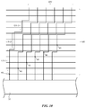
- FIG. 10 is a diagram of an illustrative gate line pattern in which vertical segments of each gate line have decreasing length and therefore traverse decreasing numbers of the rows of pixels as a function of increasing distance from the display driver circuitry in accordance with an embodiment.
- FIG. 11 is a diagram showing how an active gate line on which a gate line signal is being asserted may be flanked by adjacent auxiliary gate lines that are modulated with compensating signals of opposite swing direction (positive swing direction rather than negative swing direction or vice versa) to the gate line signal in accordance with an embodiment.
- FIG. 12 is a graph showing illustrative signals that may be driven onto the active and auxiliary gate lines of FIG. 11 during operation of a display in accordance with an embodiment.
- FIGS. 13 and 14 are diagrams of illustrative patterns of zigzagging gate line segments in accordance with an embodiment.
- FIG. 15 is a diagram of an illustrative gate line pattern in which non-horizontal portions of each gate line have diagonal orientations and are connected by vias to respective horizontal portions in accordance with an embodiment.
- Control circuitry 16 may include storage and processing circuitry for supporting the operation of device 10 .
- the storage and processing circuitry may include storage such as hard disk drive storage, nonvolatile memory (e.g., flash memory or other electrically-programmable-read-only memory configured to form a solid state drive), volatile memory (e.g., static or dynamic random-access-memory), etc.
- Processing circuitry in control circuitry 16 may be used to control the operation of device 10 .
- the processing circuitry may be based on one or more microprocessors, microcontrollers, digital signal processors, baseband processors, power management units, audio chips, application specific integrated circuits, etc.
- Input-output circuitry in device 10 such as input-output devices 12 may be used to allow data to be supplied to device 10 and to allow data to be provided from device 10 to external devices.
- Input-output devices 12 may include buttons, joysticks, scrolling wheels, touch pads, key pads, keyboards, microphones, speakers, tone generators, vibrators, cameras, sensors, light-emitting diodes and other status indicators, data ports, etc.
- a user can control the operation of device 10 by supplying commands through input-output devices 12 and may receive status information and other output from device 10 using the output resources of input-output devices 12 .
- Display 14 may be a touch screen display that includes a touch sensor for gathering touch input from a user or display 14 may be insensitive to touch.
- a touch sensor for display 14 may be based on an array of capacitive touch sensor electrodes, acoustic touch sensor structures, resistive touch components, force-based touch sensor structures, a light-based touch sensor, or other suitable touch sensor arrangements.
- Control circuitry 16 may be used to run software on device 10 such as operating system code and applications. During operation of device 10 , the software running on control circuitry 16 may display images on display 14 .
- Display 14 may be any suitable type of display.
- display 14 may be a liquid crystal display that includes an array of backlit liquid crystal display pixels, may be a light-emitting diode display that includes an array of light-emitting devices such as light-emitting diodes (e.g., organic light-emitting diodes, quantum dot light-emitting diodes, light-emitting diodes formed from discrete crystalline semiconductor dies, etc.), or may be any other type of display (e.g., an electrowetting display, an electrophoretic display, a plasma display, etc.).
- light-emitting diodes e.g., organic light-emitting diodes, quantum dot light-emitting diodes, light-emitting diodes formed from discrete crystalline semiconductor dies, etc.
- any other type of display e.g., an electrowetting display, an electrophoretic display, a plasma display, etc.
- FIG. 2 is a diagram of an illustrative display for device 10 .
- display 14 may have an array of pixels 22 for displaying images for a user.
- Pixels 22 may be formed from one or more display layers such as substrate layer 36 .
- Substrate 36 may be rectangular and may have four edges, may be oval, may be circular, may have both straight and curved edges, or may have other suitable shapes.
- the array of pixels 22 may be arranged to form rows and columns. There may be any suitable number of rows and columns in the array of pixels 22 (e.g., ten or more, one hundred or more, or one thousand or more). Pixels 22 may each contain subpixels of different colors.
- each pixel 22 may have a red subpixel that emits red light, a green subpixel that emits green light, and a blue subpixel that emits blue light.
- Configurations for display 14 that include subpixels of other colors may be used, if desired.
- Display driver circuitry 30 which may be located along one of the edges of display 14 , may be used to control the operation of pixels 22 .
- Display driver circuitry 30 may be formed from integrated circuits, thin-film transistor circuits, or other suitable circuitry.
- Display driver circuitry 30 of FIG. 2 may contain communications circuitry for communicating with system control circuitry such as control circuitry 16 of FIG. 1 over path 32 .
- Path 32 may be formed from traces on a flexible printed circuit or other cable.
- the control circuitry e.g., control circuitry 16 of FIG. 1
- display driver circuitry 30 may supply image data to data lines D while providing control signals on control lines such as gate lines G.
- the control signals on gate lines G may include scan line signals and emission enable control signals (e.g., in light-emitting diode displays), gate line signals for controlling rows of pixels in liquid crystal displays, and/or other control signals (gate line signals) for controlling the pixels of each row.
- There may be any suitable number of gate lines G per row of pixels 22 e.g., one or more, two or more, three or more, four or more, etc.). Configurations in which there is a single gate line G per row of pixels 22 may sometimes be described herein as an example.
- Gate lines G each include a non-horizontal (e.g., vertical) gate line portion (segment) GV and a horizontal gate line portion (GH).
- Each horizontal gate line segment GH extends horizontally across display 14 and is associated with a respective row of pixels 22 (e.g., each gate line segment GH may be used to control the gates of transistors in a given row of pixels 22 ).
- Non-horizontal gate line portions GV may extend vertically, diagonally, and/or horizontally through display 14 .
- Gate line portions GV may be used to route gate line signals (sometimes referred to as gate signals or pixel control signals) from display driver circuitry 30 to respective horizontal gate line segments GH. Each gate line portion GV is connected to a respective gate line portion GH at a respective gate line segment connection 40 . Connections 40 may be formed using vias or other suitable conductive coupling structures.
- Display 14 may have an active area AA that contains an array of pixels 22 to display images for a user.
- Display 14 may have an inactive border region such as inactive area IA that does not contain any pixels 22 for displaying images.
- Inactive area IA may contain circuitry such as display driver circuitry 30 . It is not necessary to provide inactive border areas IA along the left edge or right edge of active area AA to accommodate gate driver circuitry or other display driver circuitry, because gate line signals may be routed from display driver circuitry 30 along the lower edge of display 14 to horizontal gate line portions GH using gate line portions GV. This helps minimize or eliminate undesired display border regions.
- display 14 may include thin-film circuitry formed from layers 50 of material on substrate 36 .
- Layers 50 may include blanket films and patterned layers (e.g., dielectric, metal layers patterned to form signal lines, semiconductor layers patterned to form channel regions in transistors, etc.).
- layers 50 may include metal lines that are patterned to form data lines D and gate lines G.
- Gate lines G may include horizontal portions GH that extend perpendicularly to vertically extending data lines D.
- Gate lines G may also include portions GV that are connected to respective portions GH by respective vias such as via 40 .
- Portions GV may include at least some segments that extend parallel to data lines D, as shown in FIG. 3 .
- both data line D and gate line portion GV may extend parallel to each other into the page (i.e., so that data line D overlaps and runs above gate line portion GV).
- gate line portions GV may be provided with shapes that are not straight lines (i.e., non-straight shapes). In this way, each gate line is only overlapped by a given data line for a fraction of the length of the given data line, thereby minimizing capacitive coupling.
- An illustrative configuration for reducing capacitive coupling in this way is shown in FIG. 5 .
- gate line portions GV of gate lines G may be provided with zigzag shapes (i.e., non-straight shapes that minimize overlap between each gate line G and any given data line D). There may be one or more zigzag portions GV connected to each straight gate line portion GH with a respective via.
- any suitable non-straight zigzagging shape may be used for gate line portions GV.
- An illustrative waterfall pattern that may be used for non-horizontal gate line portions GV is shown in FIG. 6 .
- An illustrative staircase pattern that may be used for non-horizontal gate line portions GV is shown in FIG. 7 .
- Other zigzag patterns and/or combinations of these patterns may be used, if desired.
- the configurations of FIGS. 6 and 7 are merely examples.
- Connections 40 may be located at any positions along the lengths of portions GV or in proximity to portions GV, as shown in the illustrative connection layout diagrams of FIG. 8 (for a staircase gate line segment pattern) and FIG. 9 (for a waterfall gate line segment pattern).
- gate line portions GV can tolerate larger amounts of data line overlap at locations near display driver circuitry 30 than at locations that are farther from display driver circuitry 30 .
- An illustrative pattern that may be used for gate line portions GV that takes advantage of the larger tolerance for data line overlap with gate line portions GV at locations near display driver circuitry 30 is shown in FIG. 10 .
- gate line portions GV include vertical segments GV- 1 , vertical segments GV- 2 , and vertical segments GV- 3 coupled by respective horizontal segments.
- Segments GV- 1 are closer than segments GV- 2 to display driver circuitry 30 .
- Segments GV- 2 are closer to display driver circuitry 30 than segments GV- 3 .
- segments GV- 1 may overlap respective lines D (not shown in FIG. 10 ) for longer distances than segments GV- 2 and segments GV- 2 may overlap data lines D for longer than segments GV- 3 .
- Other patterns that ensure that data line overlap (vertical gate line segment length) decreases or otherwise changes as a function of increasing distance away from display driver circuitry 30 may be used if desired.
- the pattern of FIG. 10 is merely illustrative.
- FIG. 11 shows how a gate line (e.g., the portion GV of gate line G) may be flanked by adjacent auxiliary gate lines AG.
- Gate lines AG may be dummy gate lines that are not connected to any pixels 22 or horizontal gate line segments GH in gate lines G in display 14 .
- the graph of FIG. 12 shows an illustrative modulation scheme that may be used for the active and auxiliary gate lines of FIG. 11 .
- curve 70 corresponds to the signal on an active gate line such as gate line G of FIG.
- Curve 72 corresponds to the compensating signal of opposite swing that may be imposed on one or both of the auxiliary lines AG of FIG. 11 . If, for example, curve 70 is decreasing from 5 to ⁇ 5 and therefore has a negative swing (swing direction), curve 72 may be increasing from ⁇ 1 to 1 or from ⁇ 2 to ⁇ 1 or from 1 to 2 and therefore may have an opposite positive swing). Due to the use of a zigzag pattern such as a waterfall pattern, staircase pattern, or other zigzag pattern for gate line portions GV, each gate line (including the active gate line and both of the auxiliary gate lines) will have some overlap with a given data line D.
- a zigzag pattern such as a waterfall pattern, staircase pattern, or other zigzag pattern for gate line portions GV, each gate line (including the active gate line and both of the auxiliary gate lines) will have some overlap with a given data line D.
- compensating signals 72 i.e., signals with opposite swing direction
- auxiliary gate lines will therefore tend to cause a signal disruption in the date line D that is equal and opposite to the signal disruption produced by the active gate line (see, e.g., disruption 64 of FIG. 4 ), thereby ensuring that disruption to the signal on data line D will be minimized.
- a portion of the gate line metal on display 14 may be patterned to form dummy lines that help ensure that the visual appearance of the display (e.g., display reflectivity, etc.) is uniform across the surface of the display.
- dummy sections of gate line metal such as dummy lines GVD may be used to help ensure that the appearance of display 14 does not vary significantly across the surface of display 14 .
- Dummy lines GVD may be grounded, may not be connected to any of pixels 22 or any gate line portions GH, and may be electrically isolated from all of the gate line portions GH on display 14 .
- Dummy lines GVD may be formed from the same patterned metal layer that is used in forming active gate line portions GV.
- FIG. 14 shows how portions GV of gate lines G in display 14 may be divided into dummy segments and active segments.
- gate line G may have a horizontal portion GH′ that is connected to an active vertical portion GV′ at connection 40 (e.g., using a via or other coupling structure).
- Gap 80 may be formed in portion GV of gate line G. This divides the zigzag portion GV into active gate line portion (segment) GV′ and dummy gate line segment GVD′.
- Portion GVD′ may be connected to the other dummy lines in display 14 (i.e., dummy structures GVD) and may be grounded.
- each of the gate line portions GV of display 14 may be divided into active and dummy portions in this way. Dummy lines GVD may also be located on the edges of display 14 (e.g., in triangular dummy line regions of the type shown in FIGS. 13 and 14 or in regions of other shapes).
- gate lines may have non-horizontal portions that run diagonally for some or all of their length. These diagonal segments may each cross multiple data lines.
- FIG. 15 is a diagram of an illustrative gate line pattern in which the non-horizontal portions GV of each gate line have diagonal orientations and are connected by vias 40 to respective straight horizontal gate line portions GH.
Landscapes
- Physics & Mathematics (AREA)
- Engineering & Computer Science (AREA)
- General Physics & Mathematics (AREA)
- Nonlinear Science (AREA)
- Computer Hardware Design (AREA)
- Theoretical Computer Science (AREA)
- Crystallography & Structural Chemistry (AREA)
- Chemical & Material Sciences (AREA)
- Mathematical Physics (AREA)
- Optics & Photonics (AREA)
- Microelectronics & Electronic Packaging (AREA)
- Devices For Indicating Variable Information By Combining Individual Elements (AREA)
- Control Of Indicators Other Than Cathode Ray Tubes (AREA)
Abstract
Description
Claims (17)
Priority Applications (3)
| Application Number | Priority Date | Filing Date | Title |
|---|---|---|---|
| US15/162,974 US10839733B2 (en) | 2015-09-21 | 2016-05-24 | Display having gate lines with zigzag extensions |
| PCT/US2016/042254 WO2017052719A1 (en) | 2015-09-21 | 2016-07-14 | Display having gate lines with zigzag extensions |
| US15/643,367 US10288963B2 (en) | 2015-09-21 | 2017-07-06 | Display having gate lines with zigzag extensions |
Applications Claiming Priority (2)
| Application Number | Priority Date | Filing Date | Title |
|---|---|---|---|
| US201562221535P | 2015-09-21 | 2015-09-21 | |
| US15/162,974 US10839733B2 (en) | 2015-09-21 | 2016-05-24 | Display having gate lines with zigzag extensions |
Related Child Applications (1)
| Application Number | Title | Priority Date | Filing Date |
|---|---|---|---|
| US15/643,367 Continuation-In-Part US10288963B2 (en) | 2015-09-21 | 2017-07-06 | Display having gate lines with zigzag extensions |
Publications (2)
| Publication Number | Publication Date |
|---|---|
| US20170084214A1 US20170084214A1 (en) | 2017-03-23 |
| US10839733B2 true US10839733B2 (en) | 2020-11-17 |
Family
ID=58282889
Family Applications (1)
| Application Number | Title | Priority Date | Filing Date |
|---|---|---|---|
| US15/162,974 Expired - Fee Related US10839733B2 (en) | 2015-09-21 | 2016-05-24 | Display having gate lines with zigzag extensions |
Country Status (2)
| Country | Link |
|---|---|
| US (1) | US10839733B2 (en) |
| WO (1) | WO2017052719A1 (en) |
Families Citing this family (5)
| Publication number | Priority date | Publication date | Assignee | Title |
|---|---|---|---|---|
| US10459298B2 (en) * | 2017-07-27 | 2019-10-29 | Wuhan China Star Optoelectronics Technology Co., Ltd | Display device, array substrate and manufacturing method thereof |
| CN212783448U (en) * | 2019-08-20 | 2021-03-23 | 友达光电股份有限公司 | Pixel array substrate |
| KR102888423B1 (en) * | 2020-10-08 | 2025-11-19 | 삼성디스플레이 주식회사 | Display panel and display apparatus including the same |
| KR20220091701A (en) * | 2020-12-23 | 2022-07-01 | 삼성디스플레이 주식회사 | Display device |
| NL2033531B1 (en) * | 2022-11-15 | 2024-05-28 | Miortech Holding B V | An electrowetting optical tile |
Citations (16)
| Publication number | Priority date | Publication date | Assignee | Title |
|---|---|---|---|---|
| US20080018583A1 (en) * | 2004-05-28 | 2008-01-24 | Koninklijke Philips Electronics, N.V. | Non-Rectangular Display Device |
| US7508479B2 (en) | 2001-11-15 | 2009-03-24 | Samsung Electronics Co., Ltd. | Liquid crystal display |
| US20090102824A1 (en) | 2006-03-15 | 2009-04-23 | Sharp Kabushiki Kaisha | Active matrix substrate and display device using the same |
| US7548288B2 (en) | 2004-12-20 | 2009-06-16 | Samsung Electronics Co., Ltd. | Thin film transistor array panel and display device having particular data lines and pixel arrangement |
| US7965285B2 (en) | 2006-06-27 | 2011-06-21 | Samsung Electronics Co., Ltd. | Display substrate and display device having the same |
| US8345204B2 (en) | 2008-10-30 | 2013-01-01 | Lg Display Co., Ltd. | Liquid crystal display |
| US20130113766A1 (en) | 2011-11-04 | 2013-05-09 | Samsung Display Co., Ltd. | Display apparatus and method of manufacturing the same |
| US20130222218A1 (en) | 2009-01-16 | 2013-08-29 | Samsung Display Co., Ltd. | Display panel, method of driving the display panel and display apparatus for performing the same |
| US20140043306A1 (en) * | 2012-08-10 | 2014-02-13 | Lg Display Co., Ltd. | Liquid crystal display device |
| US20140071361A1 (en) * | 2012-07-24 | 2014-03-13 | Shanghai Tianma Micro-electronics Co., Ltd. | Liquid crystal display device and driving method thereof |
| US8804080B2 (en) | 2011-12-14 | 2014-08-12 | Lg Display Co., Ltd. | Liquid crystal display device and method of fabricating thereof |
| US8866707B2 (en) * | 2005-03-31 | 2014-10-21 | Semiconductor Energy Laboratory Co., Ltd. | Display device, and apparatus using the display device having a polygonal pixel electrode |
| US20150138473A1 (en) | 2013-11-18 | 2015-05-21 | Tianma Micro-Electronics Co., Ltd. | Pixel unit, pixel array structure and display device |
| US20150340001A1 (en) * | 2014-05-20 | 2015-11-26 | Samsung Display Co., Ltd. | Display apparatus |
| US20160005351A1 (en) * | 2014-07-04 | 2016-01-07 | Samsung Display Co., Ltd. | Display apparatus |
| US20170053597A1 (en) * | 2015-08-17 | 2017-02-23 | Samsung Display Co., Ltd. | Display driving integrated circuit, display device, and method of driving a display panel |
-
2016
- 2016-05-24 US US15/162,974 patent/US10839733B2/en not_active Expired - Fee Related
- 2016-07-14 WO PCT/US2016/042254 patent/WO2017052719A1/en not_active Ceased
Patent Citations (16)
| Publication number | Priority date | Publication date | Assignee | Title |
|---|---|---|---|---|
| US7508479B2 (en) | 2001-11-15 | 2009-03-24 | Samsung Electronics Co., Ltd. | Liquid crystal display |
| US20080018583A1 (en) * | 2004-05-28 | 2008-01-24 | Koninklijke Philips Electronics, N.V. | Non-Rectangular Display Device |
| US7548288B2 (en) | 2004-12-20 | 2009-06-16 | Samsung Electronics Co., Ltd. | Thin film transistor array panel and display device having particular data lines and pixel arrangement |
| US8866707B2 (en) * | 2005-03-31 | 2014-10-21 | Semiconductor Energy Laboratory Co., Ltd. | Display device, and apparatus using the display device having a polygonal pixel electrode |
| US20090102824A1 (en) | 2006-03-15 | 2009-04-23 | Sharp Kabushiki Kaisha | Active matrix substrate and display device using the same |
| US7965285B2 (en) | 2006-06-27 | 2011-06-21 | Samsung Electronics Co., Ltd. | Display substrate and display device having the same |
| US8345204B2 (en) | 2008-10-30 | 2013-01-01 | Lg Display Co., Ltd. | Liquid crystal display |
| US20130222218A1 (en) | 2009-01-16 | 2013-08-29 | Samsung Display Co., Ltd. | Display panel, method of driving the display panel and display apparatus for performing the same |
| US20130113766A1 (en) | 2011-11-04 | 2013-05-09 | Samsung Display Co., Ltd. | Display apparatus and method of manufacturing the same |
| US8804080B2 (en) | 2011-12-14 | 2014-08-12 | Lg Display Co., Ltd. | Liquid crystal display device and method of fabricating thereof |
| US20140071361A1 (en) * | 2012-07-24 | 2014-03-13 | Shanghai Tianma Micro-electronics Co., Ltd. | Liquid crystal display device and driving method thereof |
| US20140043306A1 (en) * | 2012-08-10 | 2014-02-13 | Lg Display Co., Ltd. | Liquid crystal display device |
| US20150138473A1 (en) | 2013-11-18 | 2015-05-21 | Tianma Micro-Electronics Co., Ltd. | Pixel unit, pixel array structure and display device |
| US20150340001A1 (en) * | 2014-05-20 | 2015-11-26 | Samsung Display Co., Ltd. | Display apparatus |
| US20160005351A1 (en) * | 2014-07-04 | 2016-01-07 | Samsung Display Co., Ltd. | Display apparatus |
| US20170053597A1 (en) * | 2015-08-17 | 2017-02-23 | Samsung Display Co., Ltd. | Display driving integrated circuit, display device, and method of driving a display panel |
Also Published As
| Publication number | Publication date |
|---|---|
| WO2017052719A1 (en) | 2017-03-30 |
| US20170084214A1 (en) | 2017-03-23 |
Similar Documents
| Publication | Publication Date | Title |
|---|---|---|
| US11594190B2 (en) | Displays with supplemental loading structures | |
| US10700151B2 (en) | Display with power supply mesh | |
| US11233113B2 (en) | Light-emitting diode displays | |
| US11049445B2 (en) | Electronic devices with narrow display borders | |
| US9336709B2 (en) | Displays with overlapping light-emitting diodes and gate drivers | |
| US9847051B2 (en) | Organic light-emitting diode display with minimized subpixel crosstalk | |
| US9337241B2 (en) | Pixel patterns for organic light-emitting diode display | |
| US10839753B2 (en) | High frame rate display | |
| US10756143B2 (en) | Transparent display panel and transparent display device including the same | |
| US10839733B2 (en) | Display having gate lines with zigzag extensions | |
| US10288963B2 (en) | Display having gate lines with zigzag extensions | |
| CN110164359B (en) | Display panel and display device | |
| US9490446B2 (en) | Organic light-emitting diode display with split anodes | |
| US11741904B2 (en) | High frame rate display | |
| US20230389384A1 (en) | Reducing Border Width Around a Hole in Display Active Area | |
| US10950679B1 (en) | Display having vertically driven gate and data paths | |
| US10964235B1 (en) | Electronic devices with narrow border displays | |
| CN112864199B (en) | Touch display panel and display device | |
| US11854490B1 (en) | Displays with gate driver circuitry in an active area | |
| US20240065057A1 (en) | Fanout Lines with Shielding in an Active Area |
Legal Events
| Date | Code | Title | Description |
|---|---|---|---|
| AS | Assignment |
Owner name: APPLE INC., CALIFORNIA Free format text: ASSIGNMENT OF ASSIGNORS INTEREST;ASSIGNORS:ONO, SHINYA;HUANG, CHUN-YAO;CHIU, HAO-LIN;AND OTHERS;SIGNING DATES FROM 20160511 TO 20160512;REEL/FRAME:038703/0298 |
|
| STPP | Information on status: patent application and granting procedure in general |
Free format text: RESPONSE TO NON-FINAL OFFICE ACTION ENTERED AND FORWARDED TO EXAMINER |
|
| STPP | Information on status: patent application and granting procedure in general |
Free format text: FINAL REJECTION MAILED |
|
| STPP | Information on status: patent application and granting procedure in general |
Free format text: RESPONSE AFTER FINAL ACTION FORWARDED TO EXAMINER |
|
| STPP | Information on status: patent application and granting procedure in general |
Free format text: ADVISORY ACTION MAILED |
|
| STPP | Information on status: patent application and granting procedure in general |
Free format text: DOCKETED NEW CASE - READY FOR EXAMINATION |
|
| STPP | Information on status: patent application and granting procedure in general |
Free format text: NON FINAL ACTION MAILED |
|
| STPP | Information on status: patent application and granting procedure in general |
Free format text: RESPONSE TO NON-FINAL OFFICE ACTION ENTERED AND FORWARDED TO EXAMINER |
|
| STPP | Information on status: patent application and granting procedure in general |
Free format text: ADVISORY ACTION MAILED |
|
| STPP | Information on status: patent application and granting procedure in general |
Free format text: PUBLICATIONS -- ISSUE FEE PAYMENT VERIFIED |
|
| STCF | Information on status: patent grant |
Free format text: PATENTED CASE |
|
| LAPS | Lapse for failure to pay maintenance fees |
Free format text: PATENT EXPIRED FOR FAILURE TO PAY MAINTENANCE FEES (ORIGINAL EVENT CODE: EXP.); ENTITY STATUS OF PATENT OWNER: LARGE ENTITY |
|
| STCH | Information on status: patent discontinuation |
Free format text: PATENT EXPIRED DUE TO NONPAYMENT OF MAINTENANCE FEES UNDER 37 CFR 1.362 |
|
| FP | Lapsed due to failure to pay maintenance fee |
Effective date: 20241117 |