US10833442B2 - Electrical connector with aligned contacting points between CPU and PCB - Google Patents
Electrical connector with aligned contacting points between CPU and PCB Download PDFInfo
- Publication number
- US10833442B2 US10833442B2 US16/543,649 US201916543649A US10833442B2 US 10833442 B2 US10833442 B2 US 10833442B2 US 201916543649 A US201916543649 A US 201916543649A US 10833442 B2 US10833442 B2 US 10833442B2
- Authority
- US
- United States
- Prior art keywords
- section
- transverse
- main body
- electrical connector
- contacting
- Prior art date
- Legal status (The legal status is an assumption and is not a legal conclusion. Google has not performed a legal analysis and makes no representation as to the accuracy of the status listed.)
- Active
Links
Images


Classifications
-
- H—ELECTRICITY
- H01—ELECTRIC ELEMENTS
- H01R—ELECTRICALLY-CONDUCTIVE CONNECTIONS; STRUCTURAL ASSOCIATIONS OF A PLURALITY OF MUTUALLY-INSULATED ELECTRICAL CONNECTING ELEMENTS; COUPLING DEVICES; CURRENT COLLECTORS
- H01R13/00—Details of coupling devices of the kinds covered by groups H01R12/70 or H01R24/00 - H01R33/00
- H01R13/646—Details of coupling devices of the kinds covered by groups H01R12/70 or H01R24/00 - H01R33/00 specially adapted for high-frequency, e.g. structures providing an impedance match or phase match
-
- H—ELECTRICITY
- H01—ELECTRIC ELEMENTS
- H01R—ELECTRICALLY-CONDUCTIVE CONNECTIONS; STRUCTURAL ASSOCIATIONS OF A PLURALITY OF MUTUALLY-INSULATED ELECTRICAL CONNECTING ELEMENTS; COUPLING DEVICES; CURRENT COLLECTORS
- H01R13/00—Details of coupling devices of the kinds covered by groups H01R12/70 or H01R24/00 - H01R33/00
- H01R13/02—Contact members
- H01R13/22—Contacts for co-operating by abutting
- H01R13/24—Contacts for co-operating by abutting resilient; resiliently-mounted
- H01R13/2464—Contacts for co-operating by abutting resilient; resiliently-mounted characterized by the contact point
-
- H—ELECTRICITY
- H01—ELECTRIC ELEMENTS
- H01R—ELECTRICALLY-CONDUCTIVE CONNECTIONS; STRUCTURAL ASSOCIATIONS OF A PLURALITY OF MUTUALLY-INSULATED ELECTRICAL CONNECTING ELEMENTS; COUPLING DEVICES; CURRENT COLLECTORS
- H01R12/00—Structural associations of a plurality of mutually-insulated electrical connecting elements, specially adapted for printed circuits, e.g. printed circuit boards [PCB], flat or ribbon cables, or like generally planar structures, e.g. terminal strips, terminal blocks; Coupling devices specially adapted for printed circuits, flat or ribbon cables, or like generally planar structures; Terminals specially adapted for contact with, or insertion into, printed circuits, flat or ribbon cables, or like generally planar structures
- H01R12/50—Fixed connections
- H01R12/51—Fixed connections for rigid printed circuits or like structures
- H01R12/55—Fixed connections for rigid printed circuits or like structures characterised by the terminals
- H01R12/57—Fixed connections for rigid printed circuits or like structures characterised by the terminals surface mounting terminals
-
- H—ELECTRICITY
- H01—ELECTRIC ELEMENTS
- H01R—ELECTRICALLY-CONDUCTIVE CONNECTIONS; STRUCTURAL ASSOCIATIONS OF A PLURALITY OF MUTUALLY-INSULATED ELECTRICAL CONNECTING ELEMENTS; COUPLING DEVICES; CURRENT COLLECTORS
- H01R12/00—Structural associations of a plurality of mutually-insulated electrical connecting elements, specially adapted for printed circuits, e.g. printed circuit boards [PCB], flat or ribbon cables, or like generally planar structures, e.g. terminal strips, terminal blocks; Coupling devices specially adapted for printed circuits, flat or ribbon cables, or like generally planar structures; Terminals specially adapted for contact with, or insertion into, printed circuits, flat or ribbon cables, or like generally planar structures
- H01R12/50—Fixed connections
- H01R12/51—Fixed connections for rigid printed circuits or like structures
- H01R12/55—Fixed connections for rigid printed circuits or like structures characterised by the terminals
- H01R12/58—Fixed connections for rigid printed circuits or like structures characterised by the terminals terminals for insertion into holes
- H01R12/585—Terminals having a press fit or a compliant portion and a shank passing through a hole in the printed circuit board
-
- H—ELECTRICITY
- H01—ELECTRIC ELEMENTS
- H01R—ELECTRICALLY-CONDUCTIVE CONNECTIONS; STRUCTURAL ASSOCIATIONS OF A PLURALITY OF MUTUALLY-INSULATED ELECTRICAL CONNECTING ELEMENTS; COUPLING DEVICES; CURRENT COLLECTORS
- H01R12/00—Structural associations of a plurality of mutually-insulated electrical connecting elements, specially adapted for printed circuits, e.g. printed circuit boards [PCB], flat or ribbon cables, or like generally planar structures, e.g. terminal strips, terminal blocks; Coupling devices specially adapted for printed circuits, flat or ribbon cables, or like generally planar structures; Terminals specially adapted for contact with, or insertion into, printed circuits, flat or ribbon cables, or like generally planar structures
- H01R12/70—Coupling devices
- H01R12/71—Coupling devices for rigid printing circuits or like structures
- H01R12/712—Coupling devices for rigid printing circuits or like structures co-operating with the surface of the printed circuit or with a coupling device exclusively provided on the surface of the printed circuit
- H01R12/714—Coupling devices for rigid printing circuits or like structures co-operating with the surface of the printed circuit or with a coupling device exclusively provided on the surface of the printed circuit with contacts abutting directly the printed circuit; Button contacts therefore provided on the printed circuit
-
- H—ELECTRICITY
- H01—ELECTRIC ELEMENTS
- H01R—ELECTRICALLY-CONDUCTIVE CONNECTIONS; STRUCTURAL ASSOCIATIONS OF A PLURALITY OF MUTUALLY-INSULATED ELECTRICAL CONNECTING ELEMENTS; COUPLING DEVICES; CURRENT COLLECTORS
- H01R12/00—Structural associations of a plurality of mutually-insulated electrical connecting elements, specially adapted for printed circuits, e.g. printed circuit boards [PCB], flat or ribbon cables, or like generally planar structures, e.g. terminal strips, terminal blocks; Coupling devices specially adapted for printed circuits, flat or ribbon cables, or like generally planar structures; Terminals specially adapted for contact with, or insertion into, printed circuits, flat or ribbon cables, or like generally planar structures
- H01R12/70—Coupling devices
- H01R12/71—Coupling devices for rigid printing circuits or like structures
- H01R12/712—Coupling devices for rigid printing circuits or like structures co-operating with the surface of the printed circuit or with a coupling device exclusively provided on the surface of the printed circuit
- H01R12/716—Coupling device provided on the PCB
-
- H—ELECTRICITY
- H01—ELECTRIC ELEMENTS
- H01R—ELECTRICALLY-CONDUCTIVE CONNECTIONS; STRUCTURAL ASSOCIATIONS OF A PLURALITY OF MUTUALLY-INSULATED ELECTRICAL CONNECTING ELEMENTS; COUPLING DEVICES; CURRENT COLLECTORS
- H01R13/00—Details of coupling devices of the kinds covered by groups H01R12/70 or H01R24/00 - H01R33/00
- H01R13/02—Contact members
- H01R13/22—Contacts for co-operating by abutting
- H01R13/24—Contacts for co-operating by abutting resilient; resiliently-mounted
- H01R13/2442—Contacts for co-operating by abutting resilient; resiliently-mounted with a single cantilevered beam
-
- H—ELECTRICITY
- H01—ELECTRIC ELEMENTS
- H01R—ELECTRICALLY-CONDUCTIVE CONNECTIONS; STRUCTURAL ASSOCIATIONS OF A PLURALITY OF MUTUALLY-INSULATED ELECTRICAL CONNECTING ELEMENTS; COUPLING DEVICES; CURRENT COLLECTORS
- H01R13/00—Details of coupling devices of the kinds covered by groups H01R12/70 or H01R24/00 - H01R33/00
- H01R13/02—Contact members
- H01R13/26—Pin or blade contacts for sliding co-operation on one side only
-
- H—ELECTRICITY
- H01—ELECTRIC ELEMENTS
- H01R—ELECTRICALLY-CONDUCTIVE CONNECTIONS; STRUCTURAL ASSOCIATIONS OF A PLURALITY OF MUTUALLY-INSULATED ELECTRICAL CONNECTING ELEMENTS; COUPLING DEVICES; CURRENT COLLECTORS
- H01R13/00—Details of coupling devices of the kinds covered by groups H01R12/70 or H01R24/00 - H01R33/00
- H01R13/40—Securing contact members in or to a base or case; Insulating of contact members
-
- H—ELECTRICITY
- H01—ELECTRIC ELEMENTS
- H01R—ELECTRICALLY-CONDUCTIVE CONNECTIONS; STRUCTURAL ASSOCIATIONS OF A PLURALITY OF MUTUALLY-INSULATED ELECTRICAL CONNECTING ELEMENTS; COUPLING DEVICES; CURRENT COLLECTORS
- H01R13/00—Details of coupling devices of the kinds covered by groups H01R12/70 or H01R24/00 - H01R33/00
- H01R13/646—Details of coupling devices of the kinds covered by groups H01R12/70 or H01R24/00 - H01R33/00 specially adapted for high-frequency, e.g. structures providing an impedance match or phase match
- H01R13/6473—Impedance matching
-
- H—ELECTRICITY
- H01—ELECTRIC ELEMENTS
- H01R—ELECTRICALLY-CONDUCTIVE CONNECTIONS; STRUCTURAL ASSOCIATIONS OF A PLURALITY OF MUTUALLY-INSULATED ELECTRICAL CONNECTING ELEMENTS; COUPLING DEVICES; CURRENT COLLECTORS
- H01R33/00—Coupling devices specially adapted for supporting apparatus and having one part acting as a holder providing support and electrical connection via a counterpart which is structurally associated with the apparatus, e.g. lamp holders; Separate parts thereof
- H01R33/74—Devices having four or more poles, e.g. holders for compact fluorescent lamps
-
- H—ELECTRICITY
- H01—ELECTRIC ELEMENTS
- H01R—ELECTRICALLY-CONDUCTIVE CONNECTIONS; STRUCTURAL ASSOCIATIONS OF A PLURALITY OF MUTUALLY-INSULATED ELECTRICAL CONNECTING ELEMENTS; COUPLING DEVICES; CURRENT COLLECTORS
- H01R43/00—Apparatus or processes specially adapted for manufacturing, assembling, maintaining, or repairing of line connectors or current collectors or for joining electric conductors
- H01R43/02—Apparatus or processes specially adapted for manufacturing, assembling, maintaining, or repairing of line connectors or current collectors or for joining electric conductors for soldered or welded connections
Definitions
- the invention relates to the electrical connector assembly, particularly to the electrical connector connecting the electronic package to the printed circuit board.
- the traditional socket connecting the CPU with the PCB may generally have the contacting point (of the contacting section) with the CPU and the contact point (of the mounting pad) with the PCB offset from each other at least in either direction X or direction Y, thus jeopardizing the performance during high speed transmission.
- An electrical connector includes an insulative housing and a plurality of contacts retained in the housing.
- Each of the contacts includes a vertical main body with retaining structure thereon, a mounting section split from the bottom portion of the main body with a horizontal pad at the end, a first transverse section extending from the top portion of the main body in a first transverse direction, an upward section extending upward from one end of the transverse direction, a second transverse section extending from an upper end of the upward section in a second transverse direction opposite to the first transverse direction, a curved contacting section extending from the end of the second transverse section, and a downward tip section formed at a free end of the contact section.
- a slot is formed in at least the first transverse section or further the upward section to receiving a portion of the contact when said contact is downwardly deflected by the CPU.
- FIG. 1(A) is a downward perspective view of an electrical connector according to a first embodiment of the invention
- FIG. 1(B) is an upward perspective view of the electrical connector of FIG. 1(A) ;
- FIG. 2(A) is an downward exploded perspective view of the electrical connector of FIG. 1(A) ;
- FIG. 2(B) is an upward exploded perspective view of the electrical connector of FIG. 1(B) ;
- FIG. 3(A) is a downward perspective view of the contact of the electrical connector of FIG. 1(A) ;
- FIG. 3(B) is an upward perspective view of the contact of the electrical connector of FIG. 1(B) ;
- FIG. 4(A) is cross-sectional view of the electrical connector of FIG. 1(A) when the contact is not downwardly pressed by the CPU and soldered upon the PCB;
- FIG. 4(B) is another cross-sectional view of the electrical connector of FIG. 1(A) when the connector is connected with both the CPU and the PCB and the contact is downwardly pressed;
- FIG. 5(A) is a downward perspective view of an electrical connector according to a second embodiment of the invention.
- FIG. 5(B) is an upward perspective view of the electrical connector of FIG. 5(A) ;
- FIG. 6(A) is an downward exploded perspective view of the electrical connector of FIG. 5(A) ;
- FIG. 6(B) is an upward exploded perspective view of the electrical connector of FIG. 5(B) ;
- FIG. 7(A) is a downward perspective view of the contact of the electrical connector of FIG. 5(A) ;
- FIG. 7(B) is an upward perspective view of the contact of the electrical connector of FIG. 5(B) ;
- FIG. 8(A) is cross-sectional view of the electrical connector of FIG. 5(A) when the contact is not downwardly pressed by the CPU and soldered upon the PCB;
- FIG. 8(B) is another cross-sectional view of the electrical connector of FIG. 5(A) when the connector is connected with both the CPU and the PCB and the contact is downwardly pressed;
- FIG. 9(A) is a downward perspective view of an electrical connector according to a third embodiment of the invention.
- FIG. 9(B) is an upward perspective view of the electrical connector of FIG. 9(A) ;
- FIG. 10(A) is an downward exploded perspective view of the electrical connector of FIG. 9(A) ;
- FIG. 10(B) is an upward exploded perspective view of the electrical connector of FIG. 9(B) ;
- FIG. 11(A) is a downward perspective view of the contact of the electrical connector of FIG. 9(A) ;
- FIG. 11(B) is an upward perspective view of the contact of the electrical connector of FIG. 9(B) ;
- FIG. 12(A) is cross-sectional view of the electrical connector of FIG. 9(A) when the contact is not downwardly pressed by the CPU and soldered upon the PCB;
- FIG. 12(B) is another cross-sectional view of the electrical connector of FIG. 9(A) when the connector is connected with both the CPU and the PCB and the contact is downwardly pressed;
- FIG. 13(A) is a downward perspective view of an electrical connector according to a fourth embodiment of the invention.
- FIG. 13(B) is an upward perspective view of the electrical connector of FIG. 13(A) ;
- FIG. 14(A) is an downward exploded perspective view of the electrical connector of FIG. 13(A) ;
- FIG. 14(B) is an upward exploded perspective view of the electrical connector of FIG. 13(B) ;
- FIG. 15(A) is a downward perspective view of the contact of the electrical connector of FIG. 13(A) ;
- FIG. 15(B) is an upward perspective view of the contact of the electrical connector of FIG. 13(B) ;
- FIG. 16(A) is cross-sectional view of the electrical connector of FIG. 13(A) when the contact is not downwardly pressed by the CPU and soldered upon the PCB;
- FIG. 16(B) is another cross-sectional view of the electrical connector of FIG. 1(A) when the connector is connected with both the CPU and the PCB and the contact is downwardly pressed;
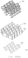
- FIG. 17 is a top view of the electrical connector of FIG. 1 ;
- FIG. 18 is a top view of the housing of the electrical connector of FIG. 1 ;
- FIG. 19 is a top view of the housing of the electrical connector of FIG. 1 with one contact shown in the dashed line;
- FIG. 20 shows the fifth embodiment of the invention.
- an electrical connector 100 includes an insulative housing 102 with a plurality of passageways 104 to retain a plurality of contacts 120 therein.
- Each contact 120 includes a main body 122 extending in a vertical plane with a pair of retaining structure 124 on two opposite lateral sides.
- a mounting section 126 is formed at a bottom portion of the main body 120 by splitting to form an opening 127 with an offset section 129 and a horizontal solder pad to which the solder ball 106 is attached on the undersurface.
- a first transverse section 130 extends from an upper portion of the main body 122 in a first transverse direction
- an upward section 132 extends from an end of the first transverse direction 130
- a second transverse section 134 extends from an upper end of the upward section 132 in a second transverse direction opposite to the first transverse direction
- a curved or upward bulged contacting section 136 is formed at a free end of the second transverse section 134 with a downward tip section 140 .
- a slot 138 extends through the first transverse direction 130 , the upward section 132 and the second transverse section 134 for enhancing resiliency thereof.
- the main body 122 abuts against an interior surface of the housing in the passageway 104 .
- the passageway 104 is composed of the lower small part 204 (B) receiving the main body 122 , and the upper large part 204 (A) receiving the first transverse section 130 and the upward section 132 .
- an electrical connector 200 includes an insulative housing 202 with a plurality of passageways 204 to retain a plurality of contacts 220 therein.
- Each of the contacts 220 includes a main body 222 extending in a vertical plane with a pair of retaining structure 224 on two opposite lateral sides.
- a mounting section 226 is split from a bottom portion of the main body 222 with an offset section 229 in an opening 227 and a horizontal solder pad to which a solder ball 206 is attached to an undersurface thereof.
- a first transverse section 230 extends from an upper portion of the main body 222 in a first transverse direction
- a curved or U-shaped upward section 232 extends from an end of the first transverse section 230 in a first transverse direction
- second transverse section 234 extends from the upward section 232 in a second transverse direction opposite to the first transverse direction
- another upward section 236 extends from an end of the second transverse section 234
- a third transverse section 238 extends from the another upward section 236 in a third transverse direction which is same with the first transverse direction
- a curved contacting section 240 is formed at a free end of the third transverse section 238 with a downward tip 241 .
- a slot 242 is formed in the first transverse section 230 , the upward section 232 and the second transverse section 234 .
- the passageway 204 includes a lower small part 204 (B) to receive the main body 222 and an upper large part 204 (A) to receive the first transverse section 230 , the upward section 230 , the second transverse section 234 , the another upward section 236 and the third transverse section 238 .
- an electrical connector 300 includes an insulative housing 302 with a plurality of passageways 304 retaining a plurality of contacts 320 therein.
- Each of the contacts 320 includes a main body 322 with a pair of retaining structures 324 on two opposite lateral sides.
- a mounting section 326 is split from the bottom portion of the main body 322 with an offset section 329 in an opening 327 and a solder pad to which a solder ball 306 is attached to an undersurface thereof.
- a first transverse section 330 extends from an upper portion of the main body 322 in a first transverse direction
- an upward section 332 extends from an end of the first transverse section 330
- a second transverse section 334 extends from an upper end of the upward section 332 in a second transverse direction opposite to the first transverse direction
- a third transverse section 336 further extends from a free end of the second transverse section 334 along the third transverse direction same with the second transverse direction, and downward toward the main body 322 .
- the second transverse section 334 and the third transverse section 336 may be commonly deemed as one deflected or angled transverse direction with an apex at a middle region thereof.
- a fourth transverse section 338 extends from an end of the third transverse section 336 in a fourth transverse direction same with the first transverse direction.
- a curved contacting section 340 is formed at an end of the fourth transverse section 338 with downward tip 341 .
- the fourth transverse section 338 may be deemed as a lower portion of the contacting section 340 during operation.
- a slot 342 is formed in a joint region between the main body 322 and the first transverse section 330 . During mating, an joint between the third transverse section 336 and the fourth transverse section 338 is received within the slot 342 .
- the passageway 304 includes lower small part 304 (B) to receive the main body 322 and an upper large part 304 (A) to receive the first transverse section 330 and the upward section 332 .
- the electrical connector 400 is very similar to the third connector 300 including the housing 402 , the passageways 404 , the solder ball 406 and the contact 420 .
- Each contact 420 has the main body 422 , the retaining structures 424 , the offset section 429 , the mounting section 426 , the opening 427 , the first transverse section 430 , the upward section 432 , the second transverse section 434 , the third transverse section 436 , the fourth transverse section 438 , the contacting section 440 , the tip 441 and the slot 442 .
- the passageway 404 includes a lower small part 404 (B) and a large upper part 404 (A).
- an additional abutment tab 444 split from the slot 442 extends upward to abut against an interior surface of the housing 402 in the upper large part 404 (A) to confront the fourth transverse section 438 intimately.
- the upper large part 104 (A) is formed by four upwardly extending posts 105 which are arranged in a diamond shape beneficial for heat dissipation and contact extending configuration/dimension consideration, and the passageway 104 is offset from a half pitch with regard to that in the neighboring row either in direction X or direction Y.
- the post 105 may by regarded as the standoffs extending from a seating plane which is a boundary/interface between the upper large part 104 (A) and the lower small part 104 (B).
- FIG. 20 shows another embodiment similar to the foregoing embodiments.
Abstract
Description
Claims (16)
Priority Applications (1)
| Application Number | Priority Date | Filing Date | Title |
|---|---|---|---|
| US16/543,649 US10833442B2 (en) | 2018-08-17 | 2019-08-19 | Electrical connector with aligned contacting points between CPU and PCB |
Applications Claiming Priority (2)
| Application Number | Priority Date | Filing Date | Title |
|---|---|---|---|
| US201862719537P | 2018-08-17 | 2018-08-17 | |
| US16/543,649 US10833442B2 (en) | 2018-08-17 | 2019-08-19 | Electrical connector with aligned contacting points between CPU and PCB |
Publications (2)
| Publication Number | Publication Date |
|---|---|
| US20200059028A1 US20200059028A1 (en) | 2020-02-20 |
| US10833442B2 true US10833442B2 (en) | 2020-11-10 |
Family
ID=69523476
Family Applications (1)
| Application Number | Title | Priority Date | Filing Date |
|---|---|---|---|
| US16/543,649 Active US10833442B2 (en) | 2018-08-17 | 2019-08-19 | Electrical connector with aligned contacting points between CPU and PCB |
Country Status (3)
| Country | Link |
|---|---|
| US (1) | US10833442B2 (en) |
| CN (1) | CN110890651B (en) |
| TW (1) | TWI813739B (en) |
Cited By (1)
| Publication number | Priority date | Publication date | Assignee | Title |
|---|---|---|---|---|
| US11309646B2 (en) * | 2019-10-22 | 2022-04-19 | Lotes Co., Ltd | Electrical connector having terminals with reduced height |
Citations (23)
| Publication number | Priority date | Publication date | Assignee | Title |
|---|---|---|---|---|
| US6315621B1 (en) * | 1999-02-18 | 2001-11-13 | Japan Aviation Electronics Industry, Limited | Electrical connector contact element having multi-contact points to come into contact with a single mating contact element with independent contacting forces |
| US6688893B1 (en) * | 2002-11-13 | 2004-02-10 | Hon Hai Precision Ind. Co., Ltd. | Electrical connector having high performance contacts |
| US6695628B2 (en) * | 2002-05-17 | 2004-02-24 | Hon Hai Precision Ind. Co., Ltd. | Battery connector |
| US6851986B2 (en) * | 2002-05-24 | 2005-02-08 | Molex Incorporated | Battery to circuit board electrical connector |
| US6976851B2 (en) * | 2003-07-04 | 2005-12-20 | Hon Hai Precision Ind. Co., Ltd. | Electrical connector having minimal wiping terminals |
| US6984130B2 (en) * | 2002-08-23 | 2006-01-10 | Lumberg Connect Gmbh & Co. Kg | Electrical contact assembly for connecting a battery to a circuit |
| US7052284B2 (en) * | 2004-04-16 | 2006-05-30 | Hon Hai Precision Ind. Co., Ltd. | Electrical contact having shorting member with reduced self-inductance |
| US7278892B1 (en) * | 2006-06-02 | 2007-10-09 | Advanced Connectek Inc. | Connector for a battery |
| US7341485B2 (en) * | 2006-07-24 | 2008-03-11 | Hon Hai Precision Ind. Co., Ltd. | Land grid array socket |
| US7559811B1 (en) * | 2008-09-30 | 2009-07-14 | Hon Hai Precision Ind. Co., Ltd. | Terminal with reduced contact tip |
| US20090253287A1 (en) * | 2008-04-03 | 2009-10-08 | Hon Hai Precision Ind. Co., Ltd. | Electrical connector with LGA contacts |
| US20110086558A1 (en) * | 2009-10-14 | 2011-04-14 | Hon Hai Precision Industry Co., Ltd. | Electrical contact with improved material and method manufacturing the same |
| US8033870B2 (en) * | 2009-12-23 | 2011-10-11 | Hon Hai Precision Ind. Co., Ltd. | Electrical connector having contact terminal with cutout receiving deprressed contact arm |
| US8096836B2 (en) * | 2009-03-09 | 2012-01-17 | Hon Hai Precision Ind. Co., Ltd | Electrical connector with contacts having tail portions with a different pitch than or discrete from contact portions of the contacts |
| US8123574B2 (en) * | 2009-01-20 | 2012-02-28 | Hon Hai Precision Ind. Co. Ltd. | Contact having increased resilience for use with electrical connector |
| US8187009B2 (en) * | 2009-11-20 | 2012-05-29 | Hon Hai Precision Ind. Co., Ltd. | High density electrical connector |
| US20120196491A1 (en) * | 2011-01-28 | 2012-08-02 | Lotes Co., Ltd. | Electrical connector |
| US8708716B1 (en) * | 2012-11-12 | 2014-04-29 | Lotes Co., Ltd. | Electrical connector |
| US20170365947A1 (en) | 2016-06-16 | 2017-12-21 | Tyco Electronics Corporation | Interposer socket and connector assembly |
| US10116080B1 (en) * | 2017-07-14 | 2018-10-30 | Lotes Co., Ltd | Electrical connector and electronic device |
| US20180331441A1 (en) | 2017-05-12 | 2018-11-15 | Lotes Co., Ltd. | Electrical connector |
| US10148023B1 (en) * | 2017-09-15 | 2018-12-04 | Lotes Co., Ltd | Electrical connector |
| US20190140383A1 (en) * | 2017-11-06 | 2019-05-09 | Lotes Co., Ltd. | Terminal and manufacturing method thereof |
Family Cites Families (5)
| Publication number | Priority date | Publication date | Assignee | Title |
|---|---|---|---|---|
| JPH09167667A (en) * | 1995-12-15 | 1997-06-24 | Toshiba Chem Corp | Contact pin for ic socket |
| CN101227040B (en) * | 2007-01-19 | 2010-09-08 | 富士康(昆山)电脑接插件有限公司 | Electric connector terminal |
| CN101227034B (en) * | 2007-01-19 | 2012-05-23 | 富士康(昆山)电脑接插件有限公司 | Electric connector terminal |
| CN201741851U (en) * | 2010-06-04 | 2011-02-09 | 富士康(昆山)电脑接插件有限公司 | Electric connector |
| CN203707390U (en) * | 2014-01-07 | 2014-07-09 | 维林企业有限公司 | Electric connector |
-
2019
- 2019-08-15 CN CN201910751369.9A patent/CN110890651B/en active Active
- 2019-08-15 TW TW108129037A patent/TWI813739B/en active
- 2019-08-19 US US16/543,649 patent/US10833442B2/en active Active
Patent Citations (25)
| Publication number | Priority date | Publication date | Assignee | Title |
|---|---|---|---|---|
| US6315621B1 (en) * | 1999-02-18 | 2001-11-13 | Japan Aviation Electronics Industry, Limited | Electrical connector contact element having multi-contact points to come into contact with a single mating contact element with independent contacting forces |
| US6695628B2 (en) * | 2002-05-17 | 2004-02-24 | Hon Hai Precision Ind. Co., Ltd. | Battery connector |
| US6851986B2 (en) * | 2002-05-24 | 2005-02-08 | Molex Incorporated | Battery to circuit board electrical connector |
| US6984130B2 (en) * | 2002-08-23 | 2006-01-10 | Lumberg Connect Gmbh & Co. Kg | Electrical contact assembly for connecting a battery to a circuit |
| US6688893B1 (en) * | 2002-11-13 | 2004-02-10 | Hon Hai Precision Ind. Co., Ltd. | Electrical connector having high performance contacts |
| US6976851B2 (en) * | 2003-07-04 | 2005-12-20 | Hon Hai Precision Ind. Co., Ltd. | Electrical connector having minimal wiping terminals |
| US7052284B2 (en) * | 2004-04-16 | 2006-05-30 | Hon Hai Precision Ind. Co., Ltd. | Electrical contact having shorting member with reduced self-inductance |
| US7278892B1 (en) * | 2006-06-02 | 2007-10-09 | Advanced Connectek Inc. | Connector for a battery |
| US7341485B2 (en) * | 2006-07-24 | 2008-03-11 | Hon Hai Precision Ind. Co., Ltd. | Land grid array socket |
| US20090253287A1 (en) * | 2008-04-03 | 2009-10-08 | Hon Hai Precision Ind. Co., Ltd. | Electrical connector with LGA contacts |
| US7559811B1 (en) * | 2008-09-30 | 2009-07-14 | Hon Hai Precision Ind. Co., Ltd. | Terminal with reduced contact tip |
| US8123574B2 (en) * | 2009-01-20 | 2012-02-28 | Hon Hai Precision Ind. Co. Ltd. | Contact having increased resilience for use with electrical connector |
| US8096836B2 (en) * | 2009-03-09 | 2012-01-17 | Hon Hai Precision Ind. Co., Ltd | Electrical connector with contacts having tail portions with a different pitch than or discrete from contact portions of the contacts |
| US20110086558A1 (en) * | 2009-10-14 | 2011-04-14 | Hon Hai Precision Industry Co., Ltd. | Electrical contact with improved material and method manufacturing the same |
| US8187009B2 (en) * | 2009-11-20 | 2012-05-29 | Hon Hai Precision Ind. Co., Ltd. | High density electrical connector |
| US8033870B2 (en) * | 2009-12-23 | 2011-10-11 | Hon Hai Precision Ind. Co., Ltd. | Electrical connector having contact terminal with cutout receiving deprressed contact arm |
| US20120196491A1 (en) * | 2011-01-28 | 2012-08-02 | Lotes Co., Ltd. | Electrical connector |
| US8708716B1 (en) * | 2012-11-12 | 2014-04-29 | Lotes Co., Ltd. | Electrical connector |
| US20170365947A1 (en) | 2016-06-16 | 2017-12-21 | Tyco Electronics Corporation | Interposer socket and connector assembly |
| US10079443B2 (en) * | 2016-06-16 | 2018-09-18 | Te Connectivity Corporation | Interposer socket and connector assembly |
| US20180331441A1 (en) | 2017-05-12 | 2018-11-15 | Lotes Co., Ltd. | Electrical connector |
| US10276953B2 (en) * | 2017-05-12 | 2019-04-30 | Lotes Co., Ltd | Electrical connector |
| US10116080B1 (en) * | 2017-07-14 | 2018-10-30 | Lotes Co., Ltd | Electrical connector and electronic device |
| US10148023B1 (en) * | 2017-09-15 | 2018-12-04 | Lotes Co., Ltd | Electrical connector |
| US20190140383A1 (en) * | 2017-11-06 | 2019-05-09 | Lotes Co., Ltd. | Terminal and manufacturing method thereof |
Cited By (1)
| Publication number | Priority date | Publication date | Assignee | Title |
|---|---|---|---|---|
| US11309646B2 (en) * | 2019-10-22 | 2022-04-19 | Lotes Co., Ltd | Electrical connector having terminals with reduced height |
Also Published As
| Publication number | Publication date |
|---|---|
| TWI813739B (en) | 2023-09-01 |
| CN110890651B (en) | 2022-12-20 |
| TW202013826A (en) | 2020-04-01 |
| CN110890651A (en) | 2020-03-17 |
| US20200059028A1 (en) | 2020-02-20 |
Similar Documents
| Publication | Publication Date | Title |
|---|---|---|
| US8172591B2 (en) | Electrical connector assembly having electrical connector with low profile and processor with cone pins | |
| US6881070B2 (en) | LGA connector and terminal thereof | |
| US8888525B2 (en) | Electrical connector with dual arm contact | |
| US20100291774A1 (en) | Electrical socket having contact terminals arranged in fan-out pitch arrangement | |
| US6695624B1 (en) | Electrical contacts used in an electrical connector | |
| US10680374B2 (en) | Electrical contact | |
| US20110009007A1 (en) | Electrical connector having improved contacts | |
| US8475179B2 (en) | Electrical connector capable of interconnecting electronic devices having different conductive leads arrangements | |
| US6634911B1 (en) | Contact for electrical connector | |
| US11245209B2 (en) | Electrical connector between CPU and PCB | |
| US7367814B2 (en) | Electrical contacts used in an electrical connector | |
| US9130321B2 (en) | Electrical connector having contact for either BGA or LGA package | |
| US10680373B2 (en) | Electrical contact of electrical connector | |
| US7950932B2 (en) | Low profile socket connector | |
| US10804636B1 (en) | Electrical connector | |
| US10833442B2 (en) | Electrical connector with aligned contacting points between CPU and PCB | |
| US20120045946A1 (en) | Socket connector having suitable receiving solder lead from ic package | |
| US8690585B2 (en) | Electrical connector for low profile application | |
| US20070281507A1 (en) | IC contact for LGA socket | |
| US20090047805A1 (en) | Socket with solder pad | |
| US11431118B2 (en) | Electrical connector having extension arms electrically connected with electronic module, extension arms extended from connecting part and multiple connecting part | |
| US7938652B2 (en) | Low profile electrical connector | |
| US20140080330A1 (en) | Electrical contact and electrical connector used thereof | |
| US8449307B2 (en) | Socket connector having contact with multiple beams jointly grasping ball of IC package | |
| US20110053426A1 (en) | Lower profile electrical contact and electrical socket using the same |
Legal Events
| Date | Code | Title | Description |
|---|---|---|---|
| AS | Assignment |
Owner name: FOXCONN INTERCONNECT TECHNOLOGY LIMITED, CAYMAN ISLANDS Free format text: ASSIGNMENT OF ASSIGNORS INTEREST;ASSIGNOR:CHENG, CHIH-PI;REEL/FRAME:050083/0684 Effective date: 20190805 Owner name: FU DING PRECISION COMPONENT (SHEN ZHEN) CO., LTD., CHINA Free format text: ASSIGNMENT OF ASSIGNORS INTEREST;ASSIGNOR:CHENG, CHIH-PI;REEL/FRAME:050083/0684 Effective date: 20190805 |
|
| FEPP | Fee payment procedure |
Free format text: ENTITY STATUS SET TO UNDISCOUNTED (ORIGINAL EVENT CODE: BIG.); ENTITY STATUS OF PATENT OWNER: LARGE ENTITY |
|
| STPP | Information on status: patent application and granting procedure in general |
Free format text: DOCKETED NEW CASE - READY FOR EXAMINATION |
|
| STPP | Information on status: patent application and granting procedure in general |
Free format text: RESPONSE TO NON-FINAL OFFICE ACTION ENTERED AND FORWARDED TO EXAMINER |
|
| STPP | Information on status: patent application and granting procedure in general |
Free format text: NOTICE OF ALLOWANCE MAILED -- APPLICATION RECEIVED IN OFFICE OF PUBLICATIONS |
|
| STPP | Information on status: patent application and granting procedure in general |
Free format text: PUBLICATIONS -- ISSUE FEE PAYMENT VERIFIED |
|
| STCF | Information on status: patent grant |
Free format text: PATENTED CASE |