US10833288B2 - Display apparatus - Google Patents
Display apparatus Download PDFInfo
- Publication number
- US10833288B2 US10833288B2 US16/411,184 US201916411184A US10833288B2 US 10833288 B2 US10833288 B2 US 10833288B2 US 201916411184 A US201916411184 A US 201916411184A US 10833288 B2 US10833288 B2 US 10833288B2
- Authority
- US
- United States
- Prior art keywords
- substrate
- area
- sealing
- sealing member
- display apparatus
- Prior art date
- Legal status (The legal status is an assumption and is not a legal conclusion. Google has not performed a legal analysis and makes no representation as to the accuracy of the status listed.)
- Active
Links
- 238000007789 sealing Methods 0.000 claims abstract description 93
- 239000000758 substrate Substances 0.000 claims abstract description 78
- 239000010410 layer Substances 0.000 description 69
- 239000010408 film Substances 0.000 description 17
- 238000000151 deposition Methods 0.000 description 15
- 239000000463 material Substances 0.000 description 15
- 230000008021 deposition Effects 0.000 description 14
- PQXKHYXIUOZZFA-UHFFFAOYSA-M lithium fluoride Chemical compound [Li+].[F-] PQXKHYXIUOZZFA-UHFFFAOYSA-M 0.000 description 12
- 239000011368 organic material Substances 0.000 description 11
- 229920000642 polymer Polymers 0.000 description 9
- VYPSYNLAJGMNEJ-UHFFFAOYSA-N Silicium dioxide Chemical compound O=[Si]=O VYPSYNLAJGMNEJ-UHFFFAOYSA-N 0.000 description 8
- PXHVJJICTQNCMI-UHFFFAOYSA-N Nickel Chemical compound [Ni] PXHVJJICTQNCMI-UHFFFAOYSA-N 0.000 description 6
- KDLHZDBZIXYQEI-UHFFFAOYSA-N Palladium Chemical compound [Pd] KDLHZDBZIXYQEI-UHFFFAOYSA-N 0.000 description 6
- XLOMVQKBTHCTTD-UHFFFAOYSA-N Zinc monoxide Chemical compound [Zn]=O XLOMVQKBTHCTTD-UHFFFAOYSA-N 0.000 description 6
- 229910052782 aluminium Inorganic materials 0.000 description 6
- 239000011575 calcium Substances 0.000 description 6
- 238000005538 encapsulation Methods 0.000 description 6
- BASFCYQUMIYNBI-UHFFFAOYSA-N platinum Chemical compound [Pt] BASFCYQUMIYNBI-UHFFFAOYSA-N 0.000 description 6
- -1 SiNx Substances 0.000 description 5
- 239000011777 magnesium Substances 0.000 description 5
- 238000000034 method Methods 0.000 description 5
- XAGFODPZIPBFFR-UHFFFAOYSA-N aluminium Chemical compound [Al] XAGFODPZIPBFFR-UHFFFAOYSA-N 0.000 description 4
- 239000010931 gold Substances 0.000 description 4
- 229910003437 indium oxide Inorganic materials 0.000 description 4
- PJXISJQVUVHSOJ-UHFFFAOYSA-N indium(iii) oxide Chemical compound [O-2].[O-2].[O-2].[In+3].[In+3] PJXISJQVUVHSOJ-UHFFFAOYSA-N 0.000 description 4
- 239000011229 interlayer Substances 0.000 description 4
- 230000001681 protective effect Effects 0.000 description 4
- 229910052814 silicon oxide Inorganic materials 0.000 description 4
- 229910052791 calcium Inorganic materials 0.000 description 3
- JAONJTDQXUSBGG-UHFFFAOYSA-N dialuminum;dizinc;oxygen(2-) Chemical compound [O-2].[O-2].[O-2].[O-2].[O-2].[Al+3].[Al+3].[Zn+2].[Zn+2] JAONJTDQXUSBGG-UHFFFAOYSA-N 0.000 description 3
- 229910010272 inorganic material Inorganic materials 0.000 description 3
- 239000011147 inorganic material Substances 0.000 description 3
- 239000002346 layers by function Substances 0.000 description 3
- 229910052749 magnesium Inorganic materials 0.000 description 3
- 238000004519 manufacturing process Methods 0.000 description 3
- 229910052751 metal Inorganic materials 0.000 description 3
- 239000002184 metal Substances 0.000 description 3
- 238000012986 modification Methods 0.000 description 3
- 230000004048 modification Effects 0.000 description 3
- 229910021420 polycrystalline silicon Inorganic materials 0.000 description 3
- 238000012360 testing method Methods 0.000 description 3
- OYPRJOBELJOOCE-UHFFFAOYSA-N Calcium Chemical compound [Ca] OYPRJOBELJOOCE-UHFFFAOYSA-N 0.000 description 2
- FYYHWMGAXLPEAU-UHFFFAOYSA-N Magnesium Chemical compound [Mg] FYYHWMGAXLPEAU-UHFFFAOYSA-N 0.000 description 2
- URLKBWYHVLBVBO-UHFFFAOYSA-N Para-Xylene Chemical group CC1=CC=C(C)C=C1 URLKBWYHVLBVBO-UHFFFAOYSA-N 0.000 description 2
- XUIMIQQOPSSXEZ-UHFFFAOYSA-N Silicon Chemical compound [Si] XUIMIQQOPSSXEZ-UHFFFAOYSA-N 0.000 description 2
- BQCADISMDOOEFD-UHFFFAOYSA-N Silver Chemical compound [Ag] BQCADISMDOOEFD-UHFFFAOYSA-N 0.000 description 2
- 229910045601 alloy Inorganic materials 0.000 description 2
- 239000000956 alloy Substances 0.000 description 2
- 229910021417 amorphous silicon Inorganic materials 0.000 description 2
- UMIVXZPTRXBADB-UHFFFAOYSA-N benzocyclobutene Chemical compound C1=CC=C2CCC2=C1 UMIVXZPTRXBADB-UHFFFAOYSA-N 0.000 description 2
- 229910000416 bismuth oxide Inorganic materials 0.000 description 2
- 239000011651 chromium Substances 0.000 description 2
- 229910052681 coesite Inorganic materials 0.000 description 2
- 239000010949 copper Substances 0.000 description 2
- 229910052906 cristobalite Inorganic materials 0.000 description 2
- 230000003247 decreasing effect Effects 0.000 description 2
- 238000013461 design Methods 0.000 description 2
- TYIXMATWDRGMPF-UHFFFAOYSA-N dibismuth;oxygen(2-) Chemical compound [O-2].[O-2].[O-2].[Bi+3].[Bi+3] TYIXMATWDRGMPF-UHFFFAOYSA-N 0.000 description 2
- PCHJSUWPFVWCPO-UHFFFAOYSA-N gold Chemical compound [Au] PCHJSUWPFVWCPO-UHFFFAOYSA-N 0.000 description 2
- 229910052737 gold Inorganic materials 0.000 description 2
- 239000012535 impurity Substances 0.000 description 2
- 238000002347 injection Methods 0.000 description 2
- 239000007924 injection Substances 0.000 description 2
- 239000011810 insulating material Substances 0.000 description 2
- 229910052744 lithium Inorganic materials 0.000 description 2
- 239000007769 metal material Substances 0.000 description 2
- 239000000203 mixture Substances 0.000 description 2
- 229910052759 nickel Inorganic materials 0.000 description 2
- ZKATWMILCYLAPD-UHFFFAOYSA-N niobium pentoxide Inorganic materials O=[Nb](=O)O[Nb](=O)=O ZKATWMILCYLAPD-UHFFFAOYSA-N 0.000 description 2
- URLJKFSTXLNXLG-UHFFFAOYSA-N niobium(5+);oxygen(2-) Chemical compound [O-2].[O-2].[O-2].[O-2].[O-2].[Nb+5].[Nb+5] URLJKFSTXLNXLG-UHFFFAOYSA-N 0.000 description 2
- TWNQGVIAIRXVLR-UHFFFAOYSA-N oxo(oxoalumanyloxy)alumane Chemical compound O=[Al]O[Al]=O TWNQGVIAIRXVLR-UHFFFAOYSA-N 0.000 description 2
- RVTZCBVAJQQJTK-UHFFFAOYSA-N oxygen(2-);zirconium(4+) Chemical compound [O-2].[O-2].[Zr+4] RVTZCBVAJQQJTK-UHFFFAOYSA-N 0.000 description 2
- 229910052763 palladium Inorganic materials 0.000 description 2
- 229910052697 platinum Inorganic materials 0.000 description 2
- 229920003229 poly(methyl methacrylate) Polymers 0.000 description 2
- 239000004926 polymethyl methacrylate Substances 0.000 description 2
- 239000004065 semiconductor Substances 0.000 description 2
- 229910052710 silicon Inorganic materials 0.000 description 2
- 239000010703 silicon Substances 0.000 description 2
- 239000000377 silicon dioxide Substances 0.000 description 2
- 229910052709 silver Inorganic materials 0.000 description 2
- 239000004332 silver Substances 0.000 description 2
- 229910052682 stishovite Inorganic materials 0.000 description 2
- LAJZODKXOMJMPK-UHFFFAOYSA-N tellurium dioxide Chemical compound O=[Te]=O LAJZODKXOMJMPK-UHFFFAOYSA-N 0.000 description 2
- 239000010409 thin film Substances 0.000 description 2
- 239000012780 transparent material Substances 0.000 description 2
- 229910052905 tridymite Inorganic materials 0.000 description 2
- 239000011787 zinc oxide Substances 0.000 description 2
- 229910001928 zirconium oxide Inorganic materials 0.000 description 2
- VYZAMTAEIAYCRO-UHFFFAOYSA-N Chromium Chemical compound [Cr] VYZAMTAEIAYCRO-UHFFFAOYSA-N 0.000 description 1
- RYGMFSIKBFXOCR-UHFFFAOYSA-N Copper Chemical compound [Cu] RYGMFSIKBFXOCR-UHFFFAOYSA-N 0.000 description 1
- IMROMDMJAWUWLK-UHFFFAOYSA-N Ethenol Chemical compound OC=C IMROMDMJAWUWLK-UHFFFAOYSA-N 0.000 description 1
- YCKRFDGAMUMZLT-UHFFFAOYSA-N Fluorine atom Chemical compound [F] YCKRFDGAMUMZLT-UHFFFAOYSA-N 0.000 description 1
- WHXSMMKQMYFTQS-UHFFFAOYSA-N Lithium Chemical compound [Li] WHXSMMKQMYFTQS-UHFFFAOYSA-N 0.000 description 1
- ZOKXTWBITQBERF-UHFFFAOYSA-N Molybdenum Chemical compound [Mo] ZOKXTWBITQBERF-UHFFFAOYSA-N 0.000 description 1
- 229910000583 Nd alloy Inorganic materials 0.000 description 1
- 229910052779 Neodymium Inorganic materials 0.000 description 1
- ISWSIDIOOBJBQZ-UHFFFAOYSA-N Phenol Chemical compound OC1=CC=CC=C1 ISWSIDIOOBJBQZ-UHFFFAOYSA-N 0.000 description 1
- 239000004952 Polyamide Substances 0.000 description 1
- 239000004642 Polyimide Substances 0.000 description 1
- 239000004793 Polystyrene Substances 0.000 description 1
- 229910052581 Si3N4 Inorganic materials 0.000 description 1
- 229910001080 W alloy Inorganic materials 0.000 description 1
- 150000001408 amides Chemical class 0.000 description 1
- 150000008378 aryl ethers Chemical class 0.000 description 1
- QVQLCTNNEUAWMS-UHFFFAOYSA-N barium oxide Chemical compound [Ba]=O QVQLCTNNEUAWMS-UHFFFAOYSA-N 0.000 description 1
- 230000015572 biosynthetic process Effects 0.000 description 1
- 229910052804 chromium Inorganic materials 0.000 description 1
- 150000001875 compounds Chemical class 0.000 description 1
- 229910052802 copper Inorganic materials 0.000 description 1
- XCJYREBRNVKWGJ-UHFFFAOYSA-N copper(II) phthalocyanine Chemical compound [Cu+2].C12=CC=CC=C2C(N=C2[N-]C(C3=CC=CC=C32)=N2)=NC1=NC([C]1C=CC=CC1=1)=NC=1N=C1[C]3C=CC=CC3=C2[N-]1 XCJYREBRNVKWGJ-UHFFFAOYSA-N 0.000 description 1
- 238000005137 deposition process Methods 0.000 description 1
- 238000011161 development Methods 0.000 description 1
- 238000010586 diagram Methods 0.000 description 1
- AJNVQOSZGJRYEI-UHFFFAOYSA-N digallium;oxygen(2-) Chemical compound [O-2].[O-2].[O-2].[Ga+3].[Ga+3] AJNVQOSZGJRYEI-UHFFFAOYSA-N 0.000 description 1
- YWEUIGNSBFLMFL-UHFFFAOYSA-N diphosphonate Chemical compound O=P(=O)OP(=O)=O YWEUIGNSBFLMFL-UHFFFAOYSA-N 0.000 description 1
- 230000009977 dual effect Effects 0.000 description 1
- 238000005516 engineering process Methods 0.000 description 1
- 239000000945 filler Substances 0.000 description 1
- 239000011737 fluorine Substances 0.000 description 1
- 229910052731 fluorine Inorganic materials 0.000 description 1
- 229920001002 functional polymer Polymers 0.000 description 1
- 229910001195 gallium oxide Inorganic materials 0.000 description 1
- 239000011521 glass Substances 0.000 description 1
- RBTKNAXYKSUFRK-UHFFFAOYSA-N heliogen blue Chemical compound [Cu].[N-]1C2=C(C=CC=C3)C3=C1N=C([N-]1)C3=CC=CC=C3C1=NC([N-]1)=C(C=CC=C3)C3=C1N=C([N-]1)C3=CC=CC=C3C1=N2 RBTKNAXYKSUFRK-UHFFFAOYSA-N 0.000 description 1
- 230000005525 hole transport Effects 0.000 description 1
- 150000003949 imides Chemical class 0.000 description 1
- 229910052738 indium Inorganic materials 0.000 description 1
- APFVFJFRJDLVQX-UHFFFAOYSA-N indium atom Chemical compound [In] APFVFJFRJDLVQX-UHFFFAOYSA-N 0.000 description 1
- AMGQUBHHOARCQH-UHFFFAOYSA-N indium;oxotin Chemical compound [In].[Sn]=O AMGQUBHHOARCQH-UHFFFAOYSA-N 0.000 description 1
- 229910052741 iridium Inorganic materials 0.000 description 1
- GKOZUEZYRPOHIO-UHFFFAOYSA-N iridium atom Chemical compound [Ir] GKOZUEZYRPOHIO-UHFFFAOYSA-N 0.000 description 1
- 230000008018 melting Effects 0.000 description 1
- 238000002844 melting Methods 0.000 description 1
- 150000002739 metals Chemical class 0.000 description 1
- 229910052750 molybdenum Inorganic materials 0.000 description 1
- 239000011733 molybdenum Substances 0.000 description 1
- IBHBKWKFFTZAHE-UHFFFAOYSA-N n-[4-[4-(n-naphthalen-1-ylanilino)phenyl]phenyl]-n-phenylnaphthalen-1-amine Chemical compound C1=CC=CC=C1N(C=1C2=CC=CC=C2C=CC=1)C1=CC=C(C=2C=CC(=CC=2)N(C=2C=CC=CC=2)C=2C3=CC=CC=C3C=CC=2)C=C1 IBHBKWKFFTZAHE-UHFFFAOYSA-N 0.000 description 1
- QEFYFXOXNSNQGX-UHFFFAOYSA-N neodymium atom Chemical compound [Nd] QEFYFXOXNSNQGX-UHFFFAOYSA-N 0.000 description 1
- 238000000059 patterning Methods 0.000 description 1
- 239000005011 phenolic resin Substances 0.000 description 1
- DLYUQMMRRRQYAE-UHFFFAOYSA-N phosphorus pentoxide Inorganic materials O1P(O2)(=O)OP3(=O)OP1(=O)OP2(=O)O3 DLYUQMMRRRQYAE-UHFFFAOYSA-N 0.000 description 1
- 239000004033 plastic Substances 0.000 description 1
- 229920003023 plastic Polymers 0.000 description 1
- 229920002647 polyamide Polymers 0.000 description 1
- 229920002098 polyfluorene Polymers 0.000 description 1
- 229920001721 polyimide Polymers 0.000 description 1
- 238000002360 preparation method Methods 0.000 description 1
- 239000011347 resin Substances 0.000 description 1
- 229920005989 resin Polymers 0.000 description 1
- HQVNEWCFYHHQES-UHFFFAOYSA-N silicon nitride Chemical compound N12[Si]34N5[Si]62N3[Si]51N64 HQVNEWCFYHHQES-UHFFFAOYSA-N 0.000 description 1
- 239000002356 single layer Substances 0.000 description 1
- 238000004528 spin coating Methods 0.000 description 1
- TVIVIEFSHFOWTE-UHFFFAOYSA-K tri(quinolin-8-yloxy)alumane Chemical compound [Al+3].C1=CN=C2C([O-])=CC=CC2=C1.C1=CN=C2C([O-])=CC=CC2=C1.C1=CN=C2C([O-])=CC=CC2=C1 TVIVIEFSHFOWTE-UHFFFAOYSA-K 0.000 description 1
- 238000001771 vacuum deposition Methods 0.000 description 1
- GRUMUEUJTSXQOI-UHFFFAOYSA-N vanadium dioxide Chemical compound O=[V]=O GRUMUEUJTSXQOI-UHFFFAOYSA-N 0.000 description 1
- 238000007740 vapor deposition Methods 0.000 description 1
- YVTHLONGBIQYBO-UHFFFAOYSA-N zinc indium(3+) oxygen(2-) Chemical compound [O--].[Zn++].[In+3] YVTHLONGBIQYBO-UHFFFAOYSA-N 0.000 description 1
Images


Classifications
-
- H—ELECTRICITY
- H10—SEMICONDUCTOR DEVICES; ELECTRIC SOLID-STATE DEVICES NOT OTHERWISE PROVIDED FOR
- H10K—ORGANIC ELECTRIC SOLID-STATE DEVICES
- H10K50/00—Organic light-emitting devices
- H10K50/80—Constructional details
- H10K50/84—Passivation; Containers; Encapsulations
- H10K50/841—Self-supporting sealing arrangements
-
- H01L51/524—
-
- H—ELECTRICITY
- H01—ELECTRIC ELEMENTS
- H01L—SEMICONDUCTOR DEVICES NOT COVERED BY CLASS H10
- H01L23/00—Details of semiconductor or other solid state devices
- H01L23/544—Marks applied to semiconductor devices or parts, e.g. registration marks, alignment structures, wafer maps
-
- H01L27/3244—
-
- H—ELECTRICITY
- H10—SEMICONDUCTOR DEVICES; ELECTRIC SOLID-STATE DEVICES NOT OTHERWISE PROVIDED FOR
- H10K—ORGANIC ELECTRIC SOLID-STATE DEVICES
- H10K59/00—Integrated devices, or assemblies of multiple devices, comprising at least one organic light-emitting element covered by group H10K50/00
- H10K59/10—OLED displays
- H10K59/12—Active-matrix OLED [AMOLED] displays
-
- H—ELECTRICITY
- H10—SEMICONDUCTOR DEVICES; ELECTRIC SOLID-STATE DEVICES NOT OTHERWISE PROVIDED FOR
- H10K—ORGANIC ELECTRIC SOLID-STATE DEVICES
- H10K59/00—Integrated devices, or assemblies of multiple devices, comprising at least one organic light-emitting element covered by group H10K50/00
- H10K59/80—Constructional details
- H10K59/87—Passivation; Containers; Encapsulations
- H10K59/871—Self-supporting sealing arrangements
-
- H—ELECTRICITY
- H01—ELECTRIC ELEMENTS
- H01L—SEMICONDUCTOR DEVICES NOT COVERED BY CLASS H10
- H01L2223/00—Details relating to semiconductor or other solid state devices covered by the group H01L23/00
- H01L2223/544—Marks applied to semiconductor devices or parts
- H01L2223/5442—Marks applied to semiconductor devices or parts comprising non digital, non alphanumeric information, e.g. symbols
-
- H—ELECTRICITY
- H01—ELECTRIC ELEMENTS
- H01L—SEMICONDUCTOR DEVICES NOT COVERED BY CLASS H10
- H01L2223/00—Details relating to semiconductor or other solid state devices covered by the group H01L23/00
- H01L2223/544—Marks applied to semiconductor devices or parts
- H01L2223/54426—Marks applied to semiconductor devices or parts for alignment
-
- H—ELECTRICITY
- H01—ELECTRIC ELEMENTS
- H01L—SEMICONDUCTOR DEVICES NOT COVERED BY CLASS H10
- H01L2223/00—Details relating to semiconductor or other solid state devices covered by the group H01L23/00
- H01L2223/544—Marks applied to semiconductor devices or parts
- H01L2223/54473—Marks applied to semiconductor devices or parts for use after dicing
- H01L2223/54486—Located on package parts, e.g. encapsulation, leads, package substrate
-
- H01L51/0011—
-
- H—ELECTRICITY
- H10—SEMICONDUCTOR DEVICES; ELECTRIC SOLID-STATE DEVICES NOT OTHERWISE PROVIDED FOR
- H10K—ORGANIC ELECTRIC SOLID-STATE DEVICES
- H10K71/00—Manufacture or treatment specially adapted for the organic devices covered by this subclass
- H10K71/10—Deposition of organic active material
- H10K71/16—Deposition of organic active material using physical vapour deposition [PVD], e.g. vacuum deposition or sputtering
- H10K71/166—Deposition of organic active material using physical vapour deposition [PVD], e.g. vacuum deposition or sputtering using selective deposition, e.g. using a mask
Definitions
- Exemplary embodiments relate to a display apparatus.
- OLED organic light-emitting display
- An organic light-emitting display apparatus may include pixels and OLEDs.
- the degree of light emission of each OLED may be controlled by a thin-film transistor (TFT).
- TFT thin-film transistor
- Such OLEDs may include a pixel electrode electrically connected to a TFT, a counter electrode facing the pixel electrode, and an intermediate layer between the pixel electrode and the counter electrode and including an organic emission layer.
- One of the methods for forming the organic emission layer included in the intermediate layer may include a deposition method using a mask. That is, organic materials evaporated from vapor deposition sources may pass through openings in the mask to be deposited on a substrate, thereby forming the organic emission layer. Therefore, in order for the organic materials to be deposited at the proper position in the deposition process, it is very important to precisely position the mask with regard to the substrate.
- Exemplary embodiments provide an organic light-emitting display apparatus that may secure a precise mask position with regard to a substrate.
- An exemplary embodiment discloses a display apparatus including a substrate having an active area and a sealing area surrounding the active area; a display unit disposed on the active area of the substrate; a sealing member having a recess formed in the sealing area of the substrate and being concave in a direction from an edge of the substrate to the active area of the substrate or from the active area of the substrate to the edge of the substrate; and an alignment mark disposed between the recess and the edge of the substrate or between the recess and the active area of the substrate.
- FIG. 1 is a schematic perspective view of a substrate for a display apparatus, according to an exemplary embodiment.
- FIG. 2 is a schematic cross-sectional view of a pixel on a substrate shown in FIG. 1 .
- FIG. 3 is a schematic enlarged view of region A illustrated in FIG. 1 .
- FIG. 4 is an enlarged schematic view of a portion of a display apparatus according to another exemplary embodiment of the inventive concept.
- FIG. 5 is an enlarged schematic view of a portion of a display apparatus according to still another exemplary embodiment of the inventive concept.
- FIG. 6 is an enlarged schematic view of a portion of a display apparatus according to still another exemplary embodiment of the inventive concept.
- FIG. 7 is an enlarged schematic view of a portion of a display apparatus according to still another exemplary embodiment of the inventive concept.
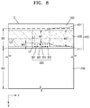
- FIG. 8 is an enlarged schematic view of a portion of a display apparatus according to still another exemplary embodiment of the inventive concept.
- an element or layer When an element or layer is referred to as being “on,” “connected to,” or “coupled to” another element or layer, it may be directly on, connected to, or coupled to the other element or layer or intervening elements or layers may be present. When, however, an element or layer is referred to as being “directly on,” “directly connected to,” or “directly coupled to” another element or layer, there are no intervening elements or layers present.
- “at least one of X, Y, and Z” and “at least one selected from the group consisting of X, Y, and Z” may be construed as X only, Y only, Z only, or any combination of two or more of X, Y, and Z, such as, for instance, XYZ, XYY, YZ, and ZZ.
- Like numbers refer to like elements throughout.
- the term “and/or” includes any and all combinations of one or more of the associated listed items.
- first, second, etc. may be used herein to describe various elements, components, regions, layers, and/or sections, these elements, components, regions, layers, and/or sections should not be limited by these terms. These terms are used to distinguish one element, component, region, layer, and/or section from another element, component, region, layer, and/or section. Thus, a first element, component, region, layer, and/or section discussed below could be termed a second element, component, region, layer, and/or section without departing from the teachings of the present disclosure.
- Spatially relative terms such as “beneath,” “below,” “lower,” “above,” “upper,” and the like, may be used herein for descriptive purposes, and, thereby, to describe one element or feature's relationship to another element(s) or feature(s) as illustrated in the drawings.
- Spatially relative terms are intended to encompass different orientations of an apparatus in use, operation, and/or manufacture in addition to the orientation depicted in the drawings. For example, if the apparatus in the drawings is turned over, elements described as “below” or “beneath” other elements or features would then be oriented “above” the other elements or features.
- the exemplary term “below” can encompass both an orientation of above and below.
- the apparatus may be otherwise oriented (e.g., rotated 90 degrees or at other orientations), and, as such, the spatially relative descriptors used herein interpreted accordingly.
- exemplary embodiments are described herein with reference to sectional illustrations that are schematic illustrations of idealized exemplary embodiments and/or intermediate structures. As such, variations from the shapes of the illustrations as a result, for example, of manufacturing techniques and/or tolerances, are to be expected. Thus, exemplary embodiments disclosed herein should not be construed as limited to the particular illustrated shapes of regions, but are to include deviations in shapes that result from, for instance, manufacturing. The regions illustrated in the drawings are schematic in nature and their shapes are not intended to illustrate the actual shape of a region of a device and are not intended to be limiting.
- FIG. 1 is a schematic perspective view of a substrate for a display apparatus 1000 , according to an exemplary embodiment.
- the display apparatus 1000 may include a substrate 100 , a display unit 200 , and an alignment mark 300 .
- the substrate 100 may include an active area AA and a sealing area SA.
- the active area AA is an area in which an image is displayed to the outside of the display apparatus 1000
- the sealing area SA is an area in which an image is not displayed and which may surround the active area AA.
- the alignment mark 300 may be disposed on at least one portion of the sealing area SA. That is, the alignment mark 300 may be disposed on the sealing area SA, or may be disposed over the sealing area SA and outside the sealing area SA.
- the display unit 200 may be disposed on the active area AA.
- the display unit 200 may include one or more thin film transistors (TFTs) and display devices electrically connected to the TFTs.
- TFTs thin film transistors
- the display devices may be one or more suitable display devices according to the type of the display apparatus 1000 . However, hereinafter the use of organic light-emitting devices (OLEDs) will be described.
- FIG. 2 is a schematic cross-sectional view of a pixel on the substrate 100 shown in FIG. 1 .
- the substrate 100 may include various materials, e.g., a glass material, a metal material, or a plastic material.
- the substrate 100 may include a transparent material.
- the display apparatus 1000 is a bottom emission-type display apparatus, in which an image is displayed to the direction of the substrate 100
- the substrate 100 may include a transparent material.
- the display apparatus 1000 is a top emission-type display apparatus, in which an image is displayed away from the substrate 100
- the substrate 100 may not necessarily include a transparent material.
- a buffer layer 212 may be formed on the substrate 100 .
- the buffer layer 212 may prevent impure elements from permeating the substrate 100 , may provide a flat surface on the substrate 100 , and may include various materials capable of performing such functions.
- the buffer layer 212 may include inorganic materials, such as silicon oxide (SiO x ), silicon nitride (SiN x ), and silicon oxynitride (SiO x N y ).
- An active layer 221 may be formed on the buffer layer 212 of an inorganic semiconductor material, such as silicon, or an organic semiconductor material.
- the active layer 221 may include a source area, a drain area, and a channel area between the source area and drain area.
- the active layer 221 including the source area, the drain area, and the channel area between the source area and drain area may be formed by forming and crystallizing an amorphous silicon layer on an entire surface of the substrate 100 , forming a polycrystalline silicon layer, patterning the polycrystalline silicon layer, and respectively doping a source area and a drain area at respective edges of the polycrystalline silicon layer with impurities.
- a gate insulating film 213 may be formed on the active layer 221 .
- the gate insulating film 213 may be used to insulate the active layer 221 from a gate electrode 222 .
- the gate insulating film 213 may include an inorganic material, such as SiN x , SiO 2 , etc.
- the gate electrode 222 may be formed on the gate insulating film 213 .
- the gate electrode 222 may be connected to a gate line (not shown) transmitting on/off signals of the TFT.
- the gate electrode 222 may contain gold (Au), silver (Ag), copper (Cu), nickel (Ni), platinum (Pt), palladium (Pd), aluminum (Al), and molybdenum (Mo), and may include an alloy, such as an Al:Nd alloy, an Mo:W alloy, etc., but is not limited thereto.
- the gate electrode 222 may include various materials by taking into account various design considerations.
- An interlayer insulating film 214 formed on the gate electrode 222 , may be used to insulate the gate electrode 222 , a source electrode 223 , and a drain electrode 224 from one another.
- the interlayer insulating film 214 may include an inorganic material such as SiN x , SiO 2 , etc.
- the source electrode 223 and the drain electrode 224 may be formed on the interlayer insulating film 214 .
- the interlayer insulating film 214 and the gate insulating film 213 may expose parts of the source area and the drain area of the active layer 221 , and the source electrode 223 and the drain electrode 224 may respectively contact the exposed parts of the source area and the drain area of the active layer 221 .
- FIG. 2 Although a top gate-type TFT, in which the gate electrode 222 , the source electrode 223 , and the drain electrode 24 are sequentially formed, is illustrated in FIG. 2 , the exemplary embodiments are not limited thereto.
- the gate electrode 222 may be disposed below the active layer 221 .
- a TFT 200 a may be electrically connected to OLEDs 200 b to drive the OLEDs 200 b , and may be protected by being covered by a protective film 215 .
- the protective film 215 may include a general-purpose polymer, such as polymethyl methacrylate (PMMA) or polystyrene (PS), a polymeric derivative having a phenol-based group, an acryl-based polymer, an imide-based polymer, an aryl ether-based polymer, an amide-based polymer, a fluorine-based polymer, a p-xylene-based polymer, a vinyl alcohol-based polymer, or a mixture thereof.
- PMMA polymethyl methacrylate
- PS polystyrene
- the OLEDs 200 b may each include a pixel electrode 231 , an intermediate layer 232 , and a counter electrode 233 .
- the pixel electrode 231 may be formed on the protective film 215 , and may be electrically connected to the drain electrode 224 via a contact hole 230 which is formed in the protective film 215 .
- the pixel electrode 231 may be a transparent (translucent) electrode or a reflective electrode.
- the pixel electrode 231 may include indium tin oxide (ITO), indium zinc oxide (IZO), zinc oxide (ZnO), indium oxide (In 2 O 3 ), indium gallium oxide (IGO), or aluminum zinc oxide (AZO).
- the pixel electrode 231 may include a reflective layer including silver (Ag), magnesium (Mg), aluminum (Al), platinum (Pt), palladium (Pd), gold (Au), nickel (Ni), neodymium (Nd), iridium (Ir), chromium (Cr), or a compound thereof, and a layer including ITO, IZO, ZnO, In 2 O 3 , IGO, or AZO.
- the pixel electrode 231 is not limited thereto and may include various other materials.
- the pixel electrode 231 may have either a single-layer structure or a multilayer structure.
- the counter electrode 233 facing the pixel electrode 231 may be a transparent (translucent) electrode or a reflective electrode.
- the counter electrode 233 may include a layer including metals having a low work function, such as lithium (Li), calcium (Ca), lithium fluoride/calcium (LiF/Ca), lithium fluoride/aluminum (LiF/Al), aluminum (Al), magnesium (Mg), or a combination thereof, and a transparent (translucent) layer including ITO, IZO, ZnO, In 2 O 3 , or the like.
- the counter electrode 233 may include a layer including Li, Ca, LiF/Ca, LiF/Al, Al, Mg, or a combination thereof. Structures and materials of the counter electrode 233 are not limited thereto and may vary.
- the counter electrode 233 may allow light emitted from an organic emission layer (not shown) included in the intermediate layer 232 to pass through. That is, the light emitted from the organic emission layer (not shown) may be reflected directly or via the pixel electrode 231 , which is a reflective electrode, and may be emitted toward the counter electrode 233 .
- the display apparatus 1000 of the present exemplary embodiment is not limited to a top emission-type, and may instead be a bottom emission-type in which the light emitted from the organic emission layer (not shown) is emitted toward the substrate 100 .
- the pixel electrode 231 may be a transparent or semi-transparent electrode
- the counter electrode 233 may be a reflective electrode.
- the organic light-emitting display apparatus 1000 of the present embodiment may also be a dual emission-type in which light is emitted in both directions of front and bottom surfaces thereof.
- a pixel-defining film 216 may be formed on the first electrode 231 as an insulating material.
- the pixel-defining film 216 may include at least one organic insulating material selected from polyimide, polyamide, acryl resin, benzocyclobutene (BCB), and phenol resin, by spin coating, or the like.
- the pixel-defining film 216 may expose a region of the pixel electrode 231 , and the intermediate layer 232 with the organic emission layer may be located on the exposed region of the pixel electrode 231 .
- the intermediate layer 232 may selectively further include a functional layer, such as a hole transport layer (HTL), a hole injection layer (HIL), an electron transport layer (ETL), an electron injection layer (EIL), etc., in addition to the organic emission layer.
- a functional layer such as a hole transport layer (HTL), a hole injection layer (HIL), an electron transport layer (ETL), an electron injection layer (EIL), etc., in addition to the organic emission layer.
- the organic emission layer (not shown) included in the intermediate layer 232 may include a low molecular weight organic material or a high molecular weight organic material.
- the low molecular weight organic material may include copper phthalocyanine (CuPc), N,N′-Di(naphthalene-1-yl)-N,N′-diphenyl-benzidine (NPB), and tris-8-hydroxyquinoline aluminum (Alq3).
- the high molecular weight organic material may include a poly-phenylenevinylene (PPV)-based material and a polyfluorene-based material.
- the organic emission layer may be formed along with the pixel electrode 231 and the counter electrode 233 , and various functional layers of the intermediate layer 232 , or separately.
- the organic emission layer is formed separately from an electrode layer and a functional layer for convenience of explanation.
- a deposition mask having openings corresponding to the pattern of the organic emission layer may be used.
- the deposition mask may be disposed in close contact with the substrate 100 via a supporting implement, such as a vacuum suction implement and a magnet unit.
- the alignment mark 300 may be disposed on a surface of the substrate 100 , as shown in FIG. 1 . The alignment mark 300 will be described in detail with reference to FIG. 3 .
- the deposition mask may be a plate-shape member that has openings corresponding to the pattern of the object to be deposited.
- a material of the deposition mask may be a metal material, such as a metal of an alloy, a functional polymer, or a mixture of a polymer and a metal.
- the openings of the deposition mask may penetrate the deposition mask and include one or more slits.
- the pixel electrode 231 , the intermediate layer 232 , and the counter electrode 233 may be sequentially formed, followed by sealing the substrate 100 and an encapsulation substrate (not shown).
- the method of sealing the substrate 100 and the encapsulation substrate may include disposing a sealing member 400 between the substrate 100 and the encapsulation substrate, and then compressing the substrate 100 and the encapsulation substrate.
- the encapsulation substrate may have a form similar to that of the substrate 100 .
- the sealing member will be described with reference to FIGS. 3 to 5 .
- FIG. 3 is a schematic enlarged view of region A illustrated in FIG. 1 .
- FIG. 4 is a schematic enlarged view of a portion of a display apparatus according to another exemplary embodiment of the inventive concept.
- the length direction of the sealing member 400 is indicated as the Y direction
- the width direction of the sealing member 400 which is perpendicular to the length direction, is indicated as the X direction.
- the sealing member 400 may be located on the sealing area SA, which is outside the active area AA of the substrate 100 .
- the sealing member 400 seals a display unit from outside of the active area AA to thereby prevent impurities, such as moisture or air from outside, from permeating into the display unit.
- the sealing member 400 may include frit.
- the sealing member 400 may be formed by forming a paste including frit at the sealing area SA of the substrate 100 , and then melting and hardening the paste including the frit.
- the frit may include vanadium oxide (VO 2 ) or bismuth oxide (Bi 2 O 3 ), and may further include various materials, such as at least one of tellurium dioxide (TeO 2 ), zinc oxide (ZnO), barium oxide (BaO), niobium pentoxide (Nb 2 O 5 ), silicon oxide (SO 2 ), aluminum oxide (Al 2 O 3 ), zirconium oxide (ZrO 2 ), and phosphorus pentoxide (P 2 O 5 ).
- the sealing member 400 may also include fillers including various materials to improve sealing properties.
- the sealing member 400 may include a recess 411 , which is concave in a direction from an edge E of the substrate 100 to the active area AA.
- a portion where the recess 411 is located is referred to as a first portion 401
- a portion adjacent to the first portion 401 is referred to as a second portion 402
- a portion between the first portion 401 and the second portion 402 is referred to as a third portion 403 .
- a width W 1 of the first portion 401 may be the same as a width W 2 of the second portion 402 .
- a width W 3 of the third portion 403 connecting the first portion 401 and second portion 402 may be greater than the width W 1 of the first portion 401 and the width W 2 of the second portion 402 .
- the alignment mark 300 for aligning the substrate 100 with a deposition mask may be disposed between the concave recess 411 of the sealing member 400 and the edge E of the substrate 100 .
- the substrate 100 having the alignment mark 300 formed thereon at a predetermined position may be prepared.
- the sealing member 400 between the alignment mark 300 and the display unit 200 may be formed. Accordingly, at least one portion of the alignment mark 300 may be on the sealing area SA, thus reducing a dead space, which is unnecessary and outside the sealing area SA.
- the alignment mark 300 may include a plurality of marks.
- the alignment mark 300 may include a rod-shape first mark 301 including two long sides parallel to the X direction and/or a rod-shape second mark 302 including two long sides parallel to the Y direction.
- the first mark 301 and the second mark 302 may be spaced apart. Accordingly, a central line L 1 of the first mark 301 and a central line L 2 of the second mark 302 may be perpendicular to each other.
- the alignment mark 300 may further include a third mark 303 .
- the third mark 303 may be an organic material pattern for testing, which may be formed prior to or simultaneously with the formation of an organic emission layer.
- the third mark 303 may include a same material as that of the organic emission layer.
- One or more third marks 303 may be formed for each color pixel.
- the alignment error between the substrate 100 and a deposition mask may be determined. For example, distance differences in the X direction and the Y direction, between the point where the central line L 1 of the first mark 301 intersects the central line L 2 of the second mark 302 and the center of the third mark 303 , may be defined as the alignment error between the substrate 100 and the deposition mask.
- an opening corresponding to the third mark 303 may be formed in the deposition mask, which is an organic material pattern for testing, in addition to the openings corresponding to the organic emission layer.
- the opening corresponding to the third mark 303 may have the same size, shape, and alignment direction as the openings corresponding to the organic emission layer.
- the alignment mark 300 may further include a fourth mark 304 , in addition to the first to third marks 301 to 303 .
- the fourth mark 304 is for verifying the alignment between the substrate 100 and measuring equipment, and may have a cross shape.
- the above described plurality of marks may be disposed to be parallel to the Y direction, which is a length direction of the sealing member 400 .
- the plurality of marks may constitute one or more columns, which are each perpendicular to the Y direction.
- the first mark 301 and the second mark 302 may be in different columns and spaced apart from each other.
- several third marks 303 which are organic material patterns for testing, may be formed outside of the active area AA.
- the position, number, shape of the plurality of marks are not limited to the described exemplary embodiments, but may vary depending on a design.
- FIG. 3 illustrates that the sealing member 400 includes the recess 411 , which is concave in a direction from the edge E of the substrate 100 to the active area AA.
- the sealing member 400 may include a recess formed in the opposite direction.
- the sealing member 400 may include the recess 411 , which is concave in a direction from the active area AA of the substrate 100 to the edge E of the substrate 100 .
- the shape of the sealing member 400 may be the same as the shape of the sealing member where the sealing member 400 illustrated in FIG. 3 is symmetrically rotated about a central line LS of the sealing area SA. Therefore, the alignment mark 300 may be disposed between the concave recess 411 of the sealing member 400 and the active area AA.
- FIGS. 5 and 6 are schematic enlarged views of a portion of a display apparatus according to still another exemplary embodiment of the inventive concept.
- FIGS. 3 and 4 descriptions of portions that are the same or similar to the above described portions will not be repeated for convenience. The same is applied to the following examples and modifications.
- the sealing member 400 may include the recess 411 , which is concave in a direction from the edge E of the substrate 100 to the active area AA.
- a portion where the recess 411 is located is referred to as the first portion 401
- a portion adjacent to the first portion 401 is referred to as the second portion 402
- a portion between the first portion 401 and the second portion 402 is referred to as the third portion 403 .
- the width W 1 of the first portion 401 , the width W 2 of the second portion 402 , and the width W 3 of the third portion 403 may be the same as one another. In other words, the width of the sealing member 400 may be constant along the whole length of the sealing member 400 .
- FIG. 5 s illustrates that both edges of the third portion 403 of the sealing member 400 are curved, but the exemplary embodiments are not limited thereto. That is, both edges of the third portion 403 may be straight.
- the alignment mark 300 may be disposed between the concave recess 411 of the sealing member 400 and the edge E of the substrate 100 . Accordingly, at least one portion of the alignment mark 300 may be disposed on the sealing area SA, helping to align the substrate 100 with a deposition mask and reduce a dead space.
- FIG. 5 illustrates that the sealing member 400 includes the recess 411 , which is concave in a direction from the edge E of the substrate 100 to the active area AA.
- the sealing member 400 may include a recess formed in the opposite direction.
- the sealing member 400 may include the recess 411 , which is concave in a direction from the active area AA of the substrate 100 to the edge E of the substrate 100 .
- the shape of the sealing member 400 may be the same as that of the sealing member 400 illustrated in FIG. 5 , where the sealing member 400 is symmetrically rotated about the central line LS of the sealing area SA. Therefore, the alignment mark 300 may be disposed between the concave recess 411 of the sealing member 400 and the active area AA.
- FIGS. 7 and 8 are schematic enlarged views of a portion of a display apparatus according to still another exemplary embodiment of the inventive concept.
- FIGS. 3 and 6 descriptions of portions the same or similar to the above described portions will not be repeated for convenience.
- the sealing member 400 may include the recess 411 , which is concave in a direction from the edge E of the substrate 100 to the active area AA.
- a portion where the recess 411 is located is referred to as the first portion 401 and a portion adjacent to the first portion 401 is referred to as the second portion 402
- the width W 1 of the first portion 401 may be less than the width W 2 of the second portion 402 .
- the alignment mark 300 may be disposed between the concave recess 411 of the sealing member 400 and the edge E of the substrate 100 .
- the edges of the first portion 401 and the second portion 402 on a side of the active area AA may be aligned in a straight line. Accordingly, the width W 1 of the first portion 401 may correspond to the difference between the width W 2 of the second portion 402 and a width W 4 , which is a width in the X direction of the recess 411 .
- the alignment mark 300 may be disposed on the sealing area SA, helping to align the substrate 100 with a deposition mask and to reduce a dead space. Because the alignment mark 300 is formed on a portion of the substrate 100 , the length (in the Y direction) of the first portion 401 , which may have a decreased width of the sealing member 400 due to the alignment mark 300 , may be much less than the entire length of the sealing member 400 . Therefore, even if the sealing member 400 has the first portion 401 , problems, such as a decrease of adhesion between the substrate 100 and an encapsulation substrate, may not arise.
- FIG. 7 illustrates that the sealing member 400 includes the recess 411 , which is concave in a direction from the edge E of the substrate 100 to the active area AA.
- the sealing member 400 may include a recess formed in the opposite direction.
- the sealing member 400 may include the recess 411 , which is concave in a direction from the active area AA of the substrate 100 to the edge E of the substrate 100 .
- the shape of the sealing member 400 may be the same as that of the sealing member 400 illustrated in FIG. 7 , where the sealing member 400 is symmetrically rotated about the central line LS of the sealing area SA. Therefore, the alignment mark 300 may be disposed between the concave recess 411 of the sealing member 400 and the active area AA.
- the display apparatus may have increased mask position precision with regard to a substrate, and have a decreased dead space on the substrate.
Abstract
A display apparatus including a substrate having an active area and a sealing area surrounding the active area; a display unit disposed on the active area of the substrate and including a plurality of organic light-emitting devices; and a sealing member including a first portion, a second portion, and a third portion, the third portion disposed between the first portion and the second portion and connecting the first portion to the second portion.
Description
This application is a continuation of U.S. patent application Ser. No. 15/916,558, filed Mar. 9, 2018, which is a continuation of U.S. patent application Ser. No. 15/421,608, filed on Feb. 1, 2017, now issued as U.S. Pat. No. 9,917,275, which is a continuation of U.S. patent application Ser. No. 15/012,391, filed on Feb. 1, 2016, now issued as U.S. Pat. No. 9,595,690, and claims priority from and the benefit of Korean Patent Application No. 10-2015-0103011, filed on Jul. 21, 2015, all of which are hereby incorporated by reference for all purposes as if fully set forth herein.
Exemplary embodiments relate to a display apparatus.
The market for display apparatuses, which may include media that allow users to communicate with each other and access information, has expanded with the development of information technology. Various kinds of display apparatuses have been developed, and organic light-emitting display (OLED) apparatuses have particularly attracted attention due to their good performance, small thickness, light weight, and low power consumption.
An organic light-emitting display apparatus may include pixels and OLEDs. The degree of light emission of each OLED may be controlled by a thin-film transistor (TFT). Such OLEDs may include a pixel electrode electrically connected to a TFT, a counter electrode facing the pixel electrode, and an intermediate layer between the pixel electrode and the counter electrode and including an organic emission layer.
One of the methods for forming the organic emission layer included in the intermediate layer may include a deposition method using a mask. That is, organic materials evaporated from vapor deposition sources may pass through openings in the mask to be deposited on a substrate, thereby forming the organic emission layer. Therefore, in order for the organic materials to be deposited at the proper position in the deposition process, it is very important to precisely position the mask with regard to the substrate.
The above information disclosed in this Background section is only for enhancement of understanding of the background of the inventive concept, and, therefore, it may contain information that does not form the prior art that is already known in this country to a person of ordinary skill in the art.
Exemplary embodiments provide an organic light-emitting display apparatus that may secure a precise mask position with regard to a substrate.
Additional aspects will be set forth in part in the description which follows and, in part, will be apparent from the disclosure, or may be learned by practice of the inventive concept.
An exemplary embodiment discloses a display apparatus including a substrate having an active area and a sealing area surrounding the active area; a display unit disposed on the active area of the substrate; a sealing member having a recess formed in the sealing area of the substrate and being concave in a direction from an edge of the substrate to the active area of the substrate or from the active area of the substrate to the edge of the substrate; and an alignment mark disposed between the recess and the edge of the substrate or between the recess and the active area of the substrate.
The foregoing general description and the following detailed description are exemplary and explanatory and are intended to provide further explanation of the claimed subject matter.
The accompanying drawings, which are included to provide a further understanding of the inventive concept, and are incorporated in and constitute a part of this specification, illustrate exemplary embodiments of the inventive concept, and, together with the description, serve to explain principles of the inventive concept.
In the following description, for the purposes of explanation, numerous specific details are set forth in order to provide a thorough understanding of various exemplary embodiments. It is apparent, however, that various exemplary embodiments may be practiced without these specific details or with one or more equivalent arrangements. In other instances, well-known structures and devices are shown in block diagram form in order to avoid unnecessarily obscuring various exemplary embodiments.
In the accompanying figures, the size and relative sizes of layers, films, panels, regions, etc., may be exaggerated for clarity and descriptive purposes. Also, like reference numerals denote like elements.
When an element or layer is referred to as being “on,” “connected to,” or “coupled to” another element or layer, it may be directly on, connected to, or coupled to the other element or layer or intervening elements or layers may be present. When, however, an element or layer is referred to as being “directly on,” “directly connected to,” or “directly coupled to” another element or layer, there are no intervening elements or layers present. For the purposes of this disclosure, “at least one of X, Y, and Z” and “at least one selected from the group consisting of X, Y, and Z” may be construed as X only, Y only, Z only, or any combination of two or more of X, Y, and Z, such as, for instance, XYZ, XYY, YZ, and ZZ. Like numbers refer to like elements throughout. As used herein, the term “and/or” includes any and all combinations of one or more of the associated listed items.
Although the terms first, second, etc. may be used herein to describe various elements, components, regions, layers, and/or sections, these elements, components, regions, layers, and/or sections should not be limited by these terms. These terms are used to distinguish one element, component, region, layer, and/or section from another element, component, region, layer, and/or section. Thus, a first element, component, region, layer, and/or section discussed below could be termed a second element, component, region, layer, and/or section without departing from the teachings of the present disclosure.
Spatially relative terms, such as “beneath,” “below,” “lower,” “above,” “upper,” and the like, may be used herein for descriptive purposes, and, thereby, to describe one element or feature's relationship to another element(s) or feature(s) as illustrated in the drawings. Spatially relative terms are intended to encompass different orientations of an apparatus in use, operation, and/or manufacture in addition to the orientation depicted in the drawings. For example, if the apparatus in the drawings is turned over, elements described as “below” or “beneath” other elements or features would then be oriented “above” the other elements or features. Thus, the exemplary term “below” can encompass both an orientation of above and below. Furthermore, the apparatus may be otherwise oriented (e.g., rotated 90 degrees or at other orientations), and, as such, the spatially relative descriptors used herein interpreted accordingly.
The terminology used herein is for the purpose of describing particular embodiments and is not intended to be limiting. As used herein, the singular forms, “a,” “an,” and “the” are intended to include the plural forms as well, unless the context clearly indicates otherwise. Moreover, the terms “comprises,” “comprising,” “includes,” and/or “including,” when used in this specification, specify the presence of stated features, integers, steps, operations, elements, components, and/or groups thereof, but do not preclude the presence or addition of one or more other features, integers, steps, operations, elements, components, and/or groups thereof.
Various exemplary embodiments are described herein with reference to sectional illustrations that are schematic illustrations of idealized exemplary embodiments and/or intermediate structures. As such, variations from the shapes of the illustrations as a result, for example, of manufacturing techniques and/or tolerances, are to be expected. Thus, exemplary embodiments disclosed herein should not be construed as limited to the particular illustrated shapes of regions, but are to include deviations in shapes that result from, for instance, manufacturing. The regions illustrated in the drawings are schematic in nature and their shapes are not intended to illustrate the actual shape of a region of a device and are not intended to be limiting.
Unless otherwise defined, all terms (including technical and scientific terms) used herein have the same meaning as commonly understood by one of ordinary skill in the art to which this disclosure is a part. Terms, such as those defined in commonly used dictionaries, should be interpreted as having a meaning that is consistent with their meaning in the context of the relevant art and will not be interpreted in an idealized or overly formal sense, unless expressly so defined herein.
Referring to FIG. 1 , the display apparatus 1000 may include a substrate 100, a display unit 200, and an alignment mark 300.
The substrate 100 may include an active area AA and a sealing area SA.
The active area AA is an area in which an image is displayed to the outside of the display apparatus 1000, and the sealing area SA is an area in which an image is not displayed and which may surround the active area AA.
The alignment mark 300 may be disposed on at least one portion of the sealing area SA. That is, the alignment mark 300 may be disposed on the sealing area SA, or may be disposed over the sealing area SA and outside the sealing area SA.
The display unit 200 may be disposed on the active area AA. The display unit 200 may include one or more thin film transistors (TFTs) and display devices electrically connected to the TFTs. The display devices may be one or more suitable display devices according to the type of the display apparatus 1000. However, hereinafter the use of organic light-emitting devices (OLEDs) will be described.
The substrate 100 may include various materials, e.g., a glass material, a metal material, or a plastic material. When the display apparatus 1000 is a bottom emission-type display apparatus, in which an image is displayed to the direction of the substrate 100, the substrate 100 may include a transparent material. On the other hand, when the display apparatus 1000 is a top emission-type display apparatus, in which an image is displayed away from the substrate 100, the substrate 100 may not necessarily include a transparent material.
A buffer layer 212 may be formed on the substrate 100. The buffer layer 212 may prevent impure elements from permeating the substrate 100, may provide a flat surface on the substrate 100, and may include various materials capable of performing such functions. For example, the buffer layer 212 may include inorganic materials, such as silicon oxide (SiOx), silicon nitride (SiNx), and silicon oxynitride (SiOxNy).
An active layer 221 may be formed on the buffer layer 212 of an inorganic semiconductor material, such as silicon, or an organic semiconductor material. The active layer 221 may include a source area, a drain area, and a channel area between the source area and drain area. For example, when the active layer 221 is formed of amorphous silicon, the active layer 221 including the source area, the drain area, and the channel area between the source area and drain area may be formed by forming and crystallizing an amorphous silicon layer on an entire surface of the substrate 100, forming a polycrystalline silicon layer, patterning the polycrystalline silicon layer, and respectively doping a source area and a drain area at respective edges of the polycrystalline silicon layer with impurities.
A gate insulating film 213 may be formed on the active layer 221. The gate insulating film 213 may be used to insulate the active layer 221 from a gate electrode 222. The gate insulating film 213 may include an inorganic material, such as SiNx, SiO2, etc.
The gate electrode 222 may be formed on the gate insulating film 213. The gate electrode 222 may be connected to a gate line (not shown) transmitting on/off signals of the TFT.
The gate electrode 222 may contain gold (Au), silver (Ag), copper (Cu), nickel (Ni), platinum (Pt), palladium (Pd), aluminum (Al), and molybdenum (Mo), and may include an alloy, such as an Al:Nd alloy, an Mo:W alloy, etc., but is not limited thereto. The gate electrode 222 may include various materials by taking into account various design considerations.
An interlayer insulating film 214, formed on the gate electrode 222, may be used to insulate the gate electrode 222, a source electrode 223, and a drain electrode 224 from one another. The interlayer insulating film 214 may include an inorganic material such as SiNx, SiO2, etc.
The source electrode 223 and the drain electrode 224 may be formed on the interlayer insulating film 214. In more detail, the interlayer insulating film 214 and the gate insulating film 213 may expose parts of the source area and the drain area of the active layer 221, and the source electrode 223 and the drain electrode 224 may respectively contact the exposed parts of the source area and the drain area of the active layer 221.
Although a top gate-type TFT, in which the gate electrode 222, the source electrode 223, and the drain electrode 24 are sequentially formed, is illustrated in FIG. 2 , the exemplary embodiments are not limited thereto. The gate electrode 222 may be disposed below the active layer 221.
A TFT 200 a may be electrically connected to OLEDs 200 b to drive the OLEDs 200 b, and may be protected by being covered by a protective film 215.
The protective film 215 may include a general-purpose polymer, such as polymethyl methacrylate (PMMA) or polystyrene (PS), a polymeric derivative having a phenol-based group, an acryl-based polymer, an imide-based polymer, an aryl ether-based polymer, an amide-based polymer, a fluorine-based polymer, a p-xylene-based polymer, a vinyl alcohol-based polymer, or a mixture thereof.
The OLEDs 200 b may each include a pixel electrode 231, an intermediate layer 232, and a counter electrode 233.
The pixel electrode 231 may be formed on the protective film 215, and may be electrically connected to the drain electrode 224 via a contact hole 230 which is formed in the protective film 215.
The pixel electrode 231 may be a transparent (translucent) electrode or a reflective electrode. When the pixel electrode 231 is the transparent (translucent) electrode, the pixel electrode 231 may include indium tin oxide (ITO), indium zinc oxide (IZO), zinc oxide (ZnO), indium oxide (In2O3), indium gallium oxide (IGO), or aluminum zinc oxide (AZO). When the pixel electrode 231 is a reflective electrode, the pixel electrode 231 may include a reflective layer including silver (Ag), magnesium (Mg), aluminum (Al), platinum (Pt), palladium (Pd), gold (Au), nickel (Ni), neodymium (Nd), iridium (Ir), chromium (Cr), or a compound thereof, and a layer including ITO, IZO, ZnO, In2O3, IGO, or AZO. However, the pixel electrode 231 is not limited thereto and may include various other materials. Also, the pixel electrode 231 may have either a single-layer structure or a multilayer structure.
The counter electrode 233 facing the pixel electrode 231 may be a transparent (translucent) electrode or a reflective electrode. When the counter electrode 233 is a transparent (translucent) electrode, the counter electrode 233 may include a layer including metals having a low work function, such as lithium (Li), calcium (Ca), lithium fluoride/calcium (LiF/Ca), lithium fluoride/aluminum (LiF/Al), aluminum (Al), magnesium (Mg), or a combination thereof, and a transparent (translucent) layer including ITO, IZO, ZnO, In2O3, or the like. When the counter electrode 233 is a reflective electrode, the counter electrode 233 may include a layer including Li, Ca, LiF/Ca, LiF/Al, Al, Mg, or a combination thereof. Structures and materials of the counter electrode 233 are not limited thereto and may vary.
Thus, the counter electrode 233 may allow light emitted from an organic emission layer (not shown) included in the intermediate layer 232 to pass through. That is, the light emitted from the organic emission layer (not shown) may be reflected directly or via the pixel electrode 231, which is a reflective electrode, and may be emitted toward the counter electrode 233.
However, the display apparatus 1000 of the present exemplary embodiment is not limited to a top emission-type, and may instead be a bottom emission-type in which the light emitted from the organic emission layer (not shown) is emitted toward the substrate 100. In this case, the pixel electrode 231 may be a transparent or semi-transparent electrode, and the counter electrode 233 may be a reflective electrode. The organic light-emitting display apparatus 1000 of the present embodiment may also be a dual emission-type in which light is emitted in both directions of front and bottom surfaces thereof.
A pixel-defining film 216 may be formed on the first electrode 231 as an insulating material. The pixel-defining film 216 may include at least one organic insulating material selected from polyimide, polyamide, acryl resin, benzocyclobutene (BCB), and phenol resin, by spin coating, or the like. The pixel-defining film 216 may expose a region of the pixel electrode 231, and the intermediate layer 232 with the organic emission layer may be located on the exposed region of the pixel electrode 231.
The intermediate layer 232 may selectively further include a functional layer, such as a hole transport layer (HTL), a hole injection layer (HIL), an electron transport layer (ETL), an electron injection layer (EIL), etc., in addition to the organic emission layer.
The organic emission layer (not shown) included in the intermediate layer 232 may include a low molecular weight organic material or a high molecular weight organic material. Examples of the low molecular weight organic material may include copper phthalocyanine (CuPc), N,N′-Di(naphthalene-1-yl)-N,N′-diphenyl-benzidine (NPB), and tris-8-hydroxyquinoline aluminum (Alq3). Examples of the high molecular weight organic material may include a poly-phenylenevinylene (PPV)-based material and a polyfluorene-based material.
There are various methods of forming the organic emission layer. For example, the low molecular weight organic material or the high molecular weight organic material may be vacuum-deposited to form the organic emission layer. The organic emission layer may be formed along with the pixel electrode 231 and the counter electrode 233, and various functional layers of the intermediate layer 232, or separately. Hereinafter it will be described that the organic emission layer is formed separately from an electrode layer and a functional layer for convenience of explanation.
In order to form the organic emission layer by vacuum deposition, a deposition mask having openings corresponding to the pattern of the organic emission layer may be used. The deposition mask may be disposed in close contact with the substrate 100 via a supporting implement, such as a vacuum suction implement and a magnet unit. In order to align the deposition mask with the substrate 100, the alignment mark 300 may be disposed on a surface of the substrate 100, as shown in FIG. 1 . The alignment mark 300 will be described in detail with reference to FIG. 3 .
The deposition mask may be a plate-shape member that has openings corresponding to the pattern of the object to be deposited. A material of the deposition mask may be a metal material, such as a metal of an alloy, a functional polymer, or a mixture of a polymer and a metal. The openings of the deposition mask may penetrate the deposition mask and include one or more slits.
The pixel electrode 231, the intermediate layer 232, and the counter electrode 233 may be sequentially formed, followed by sealing the substrate 100 and an encapsulation substrate (not shown). The method of sealing the substrate 100 and the encapsulation substrate may include disposing a sealing member 400 between the substrate 100 and the encapsulation substrate, and then compressing the substrate 100 and the encapsulation substrate. The encapsulation substrate may have a form similar to that of the substrate 100. Hereinafter, the sealing member will be described with reference to FIGS. 3 to 5 .
For convenience of explanation, the length direction of the sealing member 400 is indicated as the Y direction, and the width direction of the sealing member 400, which is perpendicular to the length direction, is indicated as the X direction.
Referring to FIG. 3 , the sealing member 400 may be located on the sealing area SA, which is outside the active area AA of the substrate 100. The sealing member 400 seals a display unit from outside of the active area AA to thereby prevent impurities, such as moisture or air from outside, from permeating into the display unit.
For example, the sealing member 400 may include frit. The sealing member 400 may be formed by forming a paste including frit at the sealing area SA of the substrate 100, and then melting and hardening the paste including the frit. The frit may include vanadium oxide (VO2) or bismuth oxide (Bi2O3), and may further include various materials, such as at least one of tellurium dioxide (TeO2), zinc oxide (ZnO), barium oxide (BaO), niobium pentoxide (Nb2O5), silicon oxide (SO2), aluminum oxide (Al2O3), zirconium oxide (ZrO2), and phosphorus pentoxide (P2O5). The sealing member 400 may also include fillers including various materials to improve sealing properties.
The sealing member 400 may include a recess 411, which is concave in a direction from an edge E of the substrate 100 to the active area AA. For convenience of explanation, with regard to the sealing member 400, a portion where the recess 411 is located is referred to as a first portion 401, a portion adjacent to the first portion 401 is referred to as a second portion 402, and a portion between the first portion 401 and the second portion 402 is referred to as a third portion 403.
As shown in FIG. 3 , a width W1 of the first portion 401 may be the same as a width W2 of the second portion 402. As the sealing member 400 is first curved from the Y direction to the X direction, and then curved from the X direction to the Y direction, a width W3 of the third portion 403 connecting the first portion 401 and second portion 402 may be greater than the width W1 of the first portion 401 and the width W2 of the second portion 402.
When the sealing member 400 is formed in such a shape, the alignment mark 300 for aligning the substrate 100 with a deposition mask (not shown) may be disposed between the concave recess 411 of the sealing member 400 and the edge E of the substrate 100. Regarding the method of preparation, first, the substrate 100 having the alignment mark 300 formed thereon at a predetermined position may be prepared. After completely forming the display unit 200 on the substrate 100, the sealing member 400 between the alignment mark 300 and the display unit 200 may be formed. Accordingly, at least one portion of the alignment mark 300 may be on the sealing area SA, thus reducing a dead space, which is unnecessary and outside the sealing area SA.
The alignment mark 300 may include a plurality of marks. For example, the alignment mark 300 may include a rod-shape first mark 301 including two long sides parallel to the X direction and/or a rod-shape second mark 302 including two long sides parallel to the Y direction. The first mark 301 and the second mark 302 may be spaced apart. Accordingly, a central line L1 of the first mark 301 and a central line L2 of the second mark 302 may be perpendicular to each other.
The alignment mark 300 may further include a third mark 303. The third mark 303 may be an organic material pattern for testing, which may be formed prior to or simultaneously with the formation of an organic emission layer. The third mark 303 may include a same material as that of the organic emission layer. One or more third marks 303 may be formed for each color pixel.
In relation to the third mark 303, by using the position relationship between the first mark 301 and the second mark 302, the alignment error between the substrate 100 and a deposition mask may be determined. For example, distance differences in the X direction and the Y direction, between the point where the central line L1 of the first mark 301 intersects the central line L2 of the second mark 302 and the center of the third mark 303, may be defined as the alignment error between the substrate 100 and the deposition mask. In order to detect the alignment error between the substrate 100 and the deposition mask, an opening corresponding to the third mark 303 may be formed in the deposition mask, which is an organic material pattern for testing, in addition to the openings corresponding to the organic emission layer. The opening corresponding to the third mark 303 may have the same size, shape, and alignment direction as the openings corresponding to the organic emission layer.
The alignment mark 300 may further include a fourth mark 304, in addition to the first to third marks 301 to 303. The fourth mark 304 is for verifying the alignment between the substrate 100 and measuring equipment, and may have a cross shape.
The above described plurality of marks may be disposed to be parallel to the Y direction, which is a length direction of the sealing member 400. The plurality of marks may constitute one or more columns, which are each perpendicular to the Y direction. For example, as shown in FIG. 3 , the first mark 301 and the second mark 302 may be in different columns and spaced apart from each other. Accordingly, several third marks 303, which are organic material patterns for testing, may be formed outside of the active area AA.
In this regard, the position, number, shape of the plurality of marks are not limited to the described exemplary embodiments, but may vary depending on a design.
Referring to FIG. 4 , the sealing member 400 may include the recess 411, which is concave in a direction from the active area AA of the substrate 100 to the edge E of the substrate 100. The shape of the sealing member 400 may be the same as the shape of the sealing member where the sealing member 400 illustrated in FIG. 3 is symmetrically rotated about a central line LS of the sealing area SA. Therefore, the alignment mark 300 may be disposed between the concave recess 411 of the sealing member 400 and the active area AA.
Referring to FIG. 5 , the sealing member 400 may include the recess 411, which is concave in a direction from the edge E of the substrate 100 to the active area AA. For convenience of explanation, with regard to the sealing member 400, a portion where the recess 411 is located is referred to as the first portion 401, a portion adjacent to the first portion 401 is referred to as the second portion 402, and a portion between the first portion 401 and the second portion 402 is referred to as the third portion 403.
The width W1 of the first portion 401, the width W2 of the second portion 402, and the width W3 of the third portion 403 may be the same as one another. In other words, the width of the sealing member 400 may be constant along the whole length of the sealing member 400. FIG. 5s illustrates that both edges of the third portion 403 of the sealing member 400 are curved, but the exemplary embodiments are not limited thereto. That is, both edges of the third portion 403 may be straight.
The alignment mark 300 may be disposed between the concave recess 411 of the sealing member 400 and the edge E of the substrate 100. Accordingly, at least one portion of the alignment mark 300 may be disposed on the sealing area SA, helping to align the substrate 100 with a deposition mask and reduce a dead space.
Referring to FIG. 6 , the sealing member 400 may include the recess 411, which is concave in a direction from the active area AA of the substrate 100 to the edge E of the substrate 100. The shape of the sealing member 400 may be the same as that of the sealing member 400 illustrated in FIG. 5 , where the sealing member 400 is symmetrically rotated about the central line LS of the sealing area SA. Therefore, the alignment mark 300 may be disposed between the concave recess 411 of the sealing member 400 and the active area AA.
Referring to FIG. 7 , the sealing member 400 may include the recess 411, which is concave in a direction from the edge E of the substrate 100 to the active area AA. For convenience of explanation, with regard to the sealing member 400, a portion where the recess 411 is located is referred to as the first portion 401 and a portion adjacent to the first portion 401 is referred to as the second portion 402
The width W1 of the first portion 401 may be less than the width W2 of the second portion 402.
The alignment mark 300 may be disposed between the concave recess 411 of the sealing member 400 and the edge E of the substrate 100. In the sealing member, the edges of the first portion 401 and the second portion 402 on a side of the active area AA may be aligned in a straight line. Accordingly, the width W1 of the first portion 401 may correspond to the difference between the width W2 of the second portion 402 and a width W4, which is a width in the X direction of the recess 411.
Accordingly, at least one portion of the alignment mark 300 may be disposed on the sealing area SA, helping to align the substrate 100 with a deposition mask and to reduce a dead space. Because the alignment mark 300 is formed on a portion of the substrate 100, the length (in the Y direction) of the first portion 401, which may have a decreased width of the sealing member 400 due to the alignment mark 300, may be much less than the entire length of the sealing member 400. Therefore, even if the sealing member 400 has the first portion 401, problems, such as a decrease of adhesion between the substrate 100 and an encapsulation substrate, may not arise.
In FIG. 7 illustrates that the sealing member 400 includes the recess 411, which is concave in a direction from the edge E of the substrate 100 to the active area AA. However, the sealing member 400 may include a recess formed in the opposite direction.
Referring to FIG. 8 , the sealing member 400 may include the recess 411, which is concave in a direction from the active area AA of the substrate 100 to the edge E of the substrate 100. The shape of the sealing member 400 may be the same as that of the sealing member 400 illustrated in FIG. 7 , where the sealing member 400 is symmetrically rotated about the central line LS of the sealing area SA. Therefore, the alignment mark 300 may be disposed between the concave recess 411 of the sealing member 400 and the active area AA.
As described above, the display apparatus according to an exemplary embodiment may have increased mask position precision with regard to a substrate, and have a decreased dead space on the substrate.
Although certain exemplary embodiments and implementations have been described herein, other embodiments and modifications will be apparent from this description. Accordingly, the inventive concept is not limited to such embodiments, but rather to the broader scope of the presented claims and various obvious modifications and equivalent arrangements.
Claims (10)
1. A display apparatus comprising:
a substrate including an active area and a sealing area surrounding the active area; and
a display unit disposed in the active area of the substrate,
wherein the sealing area comprises:
a first sealing sub-area extending in a first direction;
a second sealing sub-area positioned at an opposite side of the active area from the first sealing sub-area; and
a third sealing sub-area and a fourth sealing sub-area extending in a second direction intersecting the first direction,
wherein:
the second sealing sub-area includes a sealing member comprising a first portion, a second portion, and a third portion;
the third portion is disposed between the first portion and the second portion and connects the first portion to the second portion; and
the third portion extends in a third direction different from the first direction and the second direction.
2. The display apparatus of claim 1 , wherein the first portion is located in a center of the sealing member.
3. The display apparatus of claim 1 , wherein a width of the first portion is different from a width of the second portion.
4. The display apparatus of claim 1 , wherein a width of the third portion is different from a width of the first portion.
5. The display apparatus of claim 1 , wherein the first portion and the second portion extend in the first direction.
6. A display apparatus comprising:
a substrate including an active area and a sealing area surrounding the active area; and
a display unit disposed in the active area of the substrate,
wherein the sealing area comprises:
a first sealing sub-area extending in a first direction;
a second sealing sub-area positioned at an opposite side of the active area from the first sealing sub-area; and
a third sealing sub-area and a fourth sealing sub-area extending in a second direction intersecting the first direction,
wherein:
the second sealing sub-area includes a sealing member comprising a first portion, a second portion, and a third portion;
the third portion is disposed between the first portion and the second portion and connects the first portion to the second portion; and
a width of the first portion is different from a width of the second portion.
7. The display apparatus of claim 6 , wherein the first portion is located in a center of the second sealing member.
8. The display apparatus of claim 6 , the third portion extends in a third direction different from the first direction and the second direction.
9. The display apparatus of claim 6 , wherein a width of the third portion is different from a width of the first portion.
10. The display apparatus of claim 6 , wherein the first portion and the second portion extend in the first direction.
Priority Applications (1)
| Application Number | Priority Date | Filing Date | Title |
|---|---|---|---|
| US16/411,184 US10833288B2 (en) | 2015-07-21 | 2019-05-14 | Display apparatus |
Applications Claiming Priority (6)
| Application Number | Priority Date | Filing Date | Title |
|---|---|---|---|
| KR1020150103011A KR102323357B1 (en) | 2015-07-21 | 2015-07-21 | Display apparatus |
| KR10-2015-0103011 | 2015-07-21 | ||
| US15/012,391 US9595690B2 (en) | 2015-07-21 | 2016-02-01 | Display apparatus |
| US15/421,608 US9917275B2 (en) | 2015-07-21 | 2017-02-01 | Display apparatus |
| US15/916,558 US10340474B2 (en) | 2015-07-21 | 2018-03-09 | Display apparatus |
| US16/411,184 US10833288B2 (en) | 2015-07-21 | 2019-05-14 | Display apparatus |
Related Parent Applications (1)
| Application Number | Title | Priority Date | Filing Date |
|---|---|---|---|
| US15/916,558 Continuation US10340474B2 (en) | 2015-07-21 | 2018-03-09 | Display apparatus |
Publications (2)
| Publication Number | Publication Date |
|---|---|
| US20190267565A1 US20190267565A1 (en) | 2019-08-29 |
| US10833288B2 true US10833288B2 (en) | 2020-11-10 |
Family
ID=57837525
Family Applications (4)
| Application Number | Title | Priority Date | Filing Date |
|---|---|---|---|
| US15/012,391 Active US9595690B2 (en) | 2015-07-21 | 2016-02-01 | Display apparatus |
| US15/421,608 Active US9917275B2 (en) | 2015-07-21 | 2017-02-01 | Display apparatus |
| US15/916,558 Active US10340474B2 (en) | 2015-07-21 | 2018-03-09 | Display apparatus |
| US16/411,184 Active US10833288B2 (en) | 2015-07-21 | 2019-05-14 | Display apparatus |
Family Applications Before (3)
| Application Number | Title | Priority Date | Filing Date |
|---|---|---|---|
| US15/012,391 Active US9595690B2 (en) | 2015-07-21 | 2016-02-01 | Display apparatus |
| US15/421,608 Active US9917275B2 (en) | 2015-07-21 | 2017-02-01 | Display apparatus |
| US15/916,558 Active US10340474B2 (en) | 2015-07-21 | 2018-03-09 | Display apparatus |
Country Status (2)
| Country | Link |
|---|---|
| US (4) | US9595690B2 (en) |
| KR (1) | KR102323357B1 (en) |
Families Citing this family (2)
| Publication number | Priority date | Publication date | Assignee | Title |
|---|---|---|---|---|
| KR102323357B1 (en) * | 2015-07-21 | 2021-11-09 | 삼성디스플레이 주식회사 | Display apparatus |
| CN107359285B (en) * | 2017-08-18 | 2019-03-15 | 武汉华星光电半导体显示技术有限公司 | A kind of OLED display and preparation method thereof |
Citations (8)
| Publication number | Priority date | Publication date | Assignee | Title |
|---|---|---|---|---|
| KR20060060931A (en) | 2004-12-01 | 2006-06-07 | 엘지전자 주식회사 | Method for detecting a misalignment between a substrate and a mask |
| US20060141737A1 (en) | 2003-06-24 | 2006-06-29 | Gaidis Michael C | Planar magnetic tunnel junction substrate having recessed alignment marks |
| US20060292833A1 (en) | 2005-06-27 | 2006-12-28 | Kabushiki Kaisha Toshiba | Substrate for forming semiconductor layer |
| KR20070036188A (en) | 2004-08-25 | 2007-04-02 | 가부시끼가이샤 도시바 | Image display device and manufacturing method thereof |
| US20120320502A1 (en) | 2011-06-17 | 2012-12-20 | Samsung Mobile Display Co., Ltd. | Display panel, method of manufacturing the same, and frit composition used in the display panel |
| US20140033974A1 (en) * | 2012-07-31 | 2014-02-06 | Jae-Min Hong | Mask for deposition and method for aligning the same |
| US20140159078A1 (en) | 2012-12-11 | 2014-06-12 | Samsung Display Co., Ltd. | Display device and method of manufacturing the same |
| US9917275B2 (en) | 2015-07-21 | 2018-03-13 | Samsung Display Co., Ltd. | Display apparatus |
Family Cites Families (5)
| Publication number | Priority date | Publication date | Assignee | Title |
|---|---|---|---|---|
| KR100450460B1 (en) * | 2002-08-13 | 2004-09-30 | 엘지.필립스 엘시디 주식회사 | Soft Mold for Organic Electroluminescent Device and Method for Fabricating the same |
| KR101362168B1 (en) * | 2007-12-31 | 2014-02-13 | 엘지디스플레이 주식회사 | Organic Electro Luminescence Display and Method for manufacturing the same |
| KR101468154B1 (en) * | 2008-05-22 | 2014-12-01 | 삼성디스플레이 주식회사 | Organic light emitting display device |
| JP2011017890A (en) | 2009-07-09 | 2011-01-27 | Seiko Epson Corp | Method of manufacturing electronic equipment |
| KR101785561B1 (en) * | 2011-06-16 | 2017-11-07 | 삼성디스플레이 주식회사 | Display apparatus having enhanced sealing portion |
-
2015
- 2015-07-21 KR KR1020150103011A patent/KR102323357B1/en active IP Right Grant
-
2016
- 2016-02-01 US US15/012,391 patent/US9595690B2/en active Active
-
2017
- 2017-02-01 US US15/421,608 patent/US9917275B2/en active Active
-
2018
- 2018-03-09 US US15/916,558 patent/US10340474B2/en active Active
-
2019
- 2019-05-14 US US16/411,184 patent/US10833288B2/en active Active
Patent Citations (13)
| Publication number | Priority date | Publication date | Assignee | Title |
|---|---|---|---|---|
| US20060141737A1 (en) | 2003-06-24 | 2006-06-29 | Gaidis Michael C | Planar magnetic tunnel junction substrate having recessed alignment marks |
| KR20070036188A (en) | 2004-08-25 | 2007-04-02 | 가부시끼가이샤 도시바 | Image display device and manufacturing method thereof |
| US20070126334A1 (en) * | 2004-08-25 | 2007-06-07 | Akiyoshi Nakamura | Image display unit, and method of manufacturing the same |
| KR20060060931A (en) | 2004-12-01 | 2006-06-07 | 엘지전자 주식회사 | Method for detecting a misalignment between a substrate and a mask |
| US20060292833A1 (en) | 2005-06-27 | 2006-12-28 | Kabushiki Kaisha Toshiba | Substrate for forming semiconductor layer |
| KR20120139392A (en) | 2011-06-17 | 2012-12-27 | 삼성디스플레이 주식회사 | Display panel, manufacturing method thereof and frit compostion used in the same |
| US20120320502A1 (en) | 2011-06-17 | 2012-12-20 | Samsung Mobile Display Co., Ltd. | Display panel, method of manufacturing the same, and frit composition used in the display panel |
| US20140033974A1 (en) * | 2012-07-31 | 2014-02-06 | Jae-Min Hong | Mask for deposition and method for aligning the same |
| KR20140017767A (en) | 2012-07-31 | 2014-02-12 | 삼성디스플레이 주식회사 | Mask for deposition and method for aligning the same |
| US20140159078A1 (en) | 2012-12-11 | 2014-06-12 | Samsung Display Co., Ltd. | Display device and method of manufacturing the same |
| KR20140075467A (en) | 2012-12-11 | 2014-06-19 | 삼성디스플레이 주식회사 | Display device and manufacturing method of the same |
| US9917275B2 (en) | 2015-07-21 | 2018-03-13 | Samsung Display Co., Ltd. | Display apparatus |
| US10340474B2 (en) * | 2015-07-21 | 2019-07-02 | Samsung Display Co., Ltd. | Display apparatus |
Non-Patent Citations (5)
| Title |
|---|
| Non-Final Office Action dated Jul. 18, 2018 in U.S. Appl. No. 15/916,558. |
| Non-Final Office Action dated Jun. 16, 2017 in U.S. Appl. No. 15/421,608. |
| Notice of Allowance dated May 1, 2019 in U.S. Appl. No. 15/916,558. |
| Notice of Allowance dated Nov. 1, 2016 in U.S. Appl. No. 15/012,391. |
| Notice of Allowance dated Nov. 2, 2017 in U.S. Appl. No. 15/421,608. |
Also Published As
| Publication number | Publication date |
|---|---|
| US20190267565A1 (en) | 2019-08-29 |
| US20170141343A1 (en) | 2017-05-18 |
| US20180198085A1 (en) | 2018-07-12 |
| US9595690B2 (en) | 2017-03-14 |
| US20170025632A1 (en) | 2017-01-26 |
| US9917275B2 (en) | 2018-03-13 |
| KR20170012635A (en) | 2017-02-03 |
| KR102323357B1 (en) | 2021-11-09 |
| US10340474B2 (en) | 2019-07-02 |
Similar Documents
| Publication | Publication Date | Title |
|---|---|---|
| US9997741B2 (en) | Method of manufacturing organic light emitting display apparatus | |
| US8461591B2 (en) | Organic light emitting display apparatus and method of manufacturing the same | |
| US9450185B2 (en) | Thin-film deposition mask, method of fabricating the same, and method of fabricating an organic light emitting display apparatus using the same | |
| US9088004B2 (en) | Organic light-emitting display apparatus and manufacturing method thereof | |
| US8659021B2 (en) | Organic light-emitting display device and method of manufacturing the same | |
| US8796768B2 (en) | Organic light emitting display device including nano silver particles and method of manufacturing the same | |
| JP5906020B2 (en) | Organic light emitting display device and method for manufacturing the same | |
| KR101074809B1 (en) | Organic light emitting display apparatus | |
| US20110198598A1 (en) | Organic light emitting display apparatus and method of manufacturing the same | |
| US20170133592A1 (en) | Mask frame assembly, device for deposition including the same, and method of manufacturing display device | |
| US8729552B2 (en) | Backplane for flat panel display apparatus, flat panel display apparatus including the same, and method of manufacturing backplane for flat panel display apparatus | |
| US20140353601A1 (en) | Film for display apparatus, organic light-emitting display apparatus including the same, and method of manufacturing the film | |
| US7425730B2 (en) | Organic electro-luminescent display and fabrication method thereof | |
| US10224435B2 (en) | Transistor, manufacturing method thereof, and display device including the same | |
| US9525047B2 (en) | Thin-film transistor substrate, method of manufacturing same, and organic light-emitting display apparatus including thin-film transistor substrate | |
| KR20140065276A (en) | Organic light emitting display apparatus and manufacturing method thereof | |
| EP3316312A1 (en) | Display device having emitting areas | |
| US10833288B2 (en) | Display apparatus | |
| CN103872074A (en) | Display device and method of manufacturing same | |
| KR100846589B1 (en) | Method of aligning substrate |
Legal Events
| Date | Code | Title | Description |
|---|---|---|---|
| FEPP | Fee payment procedure |
Free format text: ENTITY STATUS SET TO UNDISCOUNTED (ORIGINAL EVENT CODE: BIG.); ENTITY STATUS OF PATENT OWNER: LARGE ENTITY |
|
| STPP | Information on status: patent application and granting procedure in general |
Free format text: DOCKETED NEW CASE - READY FOR EXAMINATION |
|
| STPP | Information on status: patent application and granting procedure in general |
Free format text: NON FINAL ACTION MAILED |
|
| STPP | Information on status: patent application and granting procedure in general |
Free format text: NOTICE OF ALLOWANCE MAILED -- APPLICATION RECEIVED IN OFFICE OF PUBLICATIONS |
|
| STPP | Information on status: patent application and granting procedure in general |
Free format text: PUBLICATIONS -- ISSUE FEE PAYMENT VERIFIED |
|
| STCF | Information on status: patent grant |
Free format text: PATENTED CASE |