US10832889B2 - Charged particle beam device - Google Patents

Charged particle beam device Download PDF

Info

Publication number
US10832889B2
US10832889B2 US16/320,525 US201616320525A US10832889B2 US 10832889 B2 US10832889 B2 US 10832889B2 US 201616320525 A US201616320525 A US 201616320525A US 10832889 B2 US10832889 B2 US 10832889B2
Authority
US
United States
Prior art keywords
sample
shielding plate
ion beam
tilt
ion
Prior art date
Legal status (The legal status is an assumption and is not a legal conclusion. Google has not performed a legal analysis and makes no representation as to the accuracy of the status listed.)
Active
Application number
US16/320,525
Other versions
US20190272973A1 (en
Inventor
Asako Kaneko
Hisayuki Takasu
Toru Iwaya
Current Assignee (The listed assignees may be inaccurate. Google has not performed a legal analysis and makes no representation or warranty as to the accuracy of the list.)
Hitachi High Tech Corp
Original Assignee
Hitachi High Tech Corp
Priority date (The priority date is an assumption and is not a legal conclusion. Google has not performed a legal analysis and makes no representation as to the accuracy of the date listed.)
Filing date
Publication date
Application filed by Hitachi High Tech Corp filed Critical Hitachi High Tech Corp
Assigned to HITACHI HIGH-TECHNOLOGIES CORPORATION reassignment HITACHI HIGH-TECHNOLOGIES CORPORATION ASSIGNMENT OF ASSIGNORS INTEREST (SEE DOCUMENT FOR DETAILS). Assignors: KANEKO, ASAKO, TAKASU, HISAYUKI, IWAYA, TORU
Publication of US20190272973A1 publication Critical patent/US20190272973A1/en
Assigned to HITACHI HIGH-TECH CORPORATION reassignment HITACHI HIGH-TECH CORPORATION CHANGE OF NAME AND ADDRESS Assignors: HITACHI HIGH-TECHNOLOGIES CORPORATION
Application granted granted Critical
Publication of US10832889B2 publication Critical patent/US10832889B2/en
Active legal-status Critical Current
Anticipated expiration legal-status Critical

Links

Images

Classifications

    • HELECTRICITY
    • H01ELECTRIC ELEMENTS
    • H01JELECTRIC DISCHARGE TUBES OR DISCHARGE LAMPS
    • H01J37/00Discharge tubes with provision for introducing objects or material to be exposed to the discharge, e.g. for the purpose of examination or processing thereof
    • H01J37/02Details
    • H01J37/16Vessels; Containers
    • H01J37/165Means associated with the vessel for preventing the generation of or for shielding unwanted radiation, e.g. X-rays
    • HELECTRICITY
    • H01ELECTRIC ELEMENTS
    • H01JELECTRIC DISCHARGE TUBES OR DISCHARGE LAMPS
    • H01J37/00Discharge tubes with provision for introducing objects or material to be exposed to the discharge, e.g. for the purpose of examination or processing thereof
    • H01J37/02Details
    • H01J37/04Arrangements of electrodes and associated parts for generating or controlling the discharge, e.g. electron-optical arrangement or ion-optical arrangement
    • H01J37/09Diaphragms; Shields associated with electron or ion-optical arrangements; Compensation of disturbing fields
    • HELECTRICITY
    • H01ELECTRIC ELEMENTS
    • H01JELECTRIC DISCHARGE TUBES OR DISCHARGE LAMPS
    • H01J37/00Discharge tubes with provision for introducing objects or material to be exposed to the discharge, e.g. for the purpose of examination or processing thereof
    • H01J37/02Details
    • H01J37/20Means for supporting or positioning the object or the material; Means for adjusting diaphragms or lenses associated with the support
    • HELECTRICITY
    • H01ELECTRIC ELEMENTS
    • H01JELECTRIC DISCHARGE TUBES OR DISCHARGE LAMPS
    • H01J37/00Discharge tubes with provision for introducing objects or material to be exposed to the discharge, e.g. for the purpose of examination or processing thereof
    • H01J37/30Electron-beam or ion-beam tubes for localised treatment of objects
    • H01J37/305Electron-beam or ion-beam tubes for localised treatment of objects for casting, melting, evaporating, or etching
    • H01J37/3053Electron-beam or ion-beam tubes for localised treatment of objects for casting, melting, evaporating, or etching for evaporating or etching
    • H01J37/3056Electron-beam or ion-beam tubes for localised treatment of objects for casting, melting, evaporating, or etching for evaporating or etching for microworking, e. g. etching of gratings or trimming of electrical components
    • HELECTRICITY
    • H01ELECTRIC ELEMENTS
    • H01JELECTRIC DISCHARGE TUBES OR DISCHARGE LAMPS
    • H01J2237/00Discharge tubes exposing object to beam, e.g. for analysis treatment, etching, imaging
    • H01J2237/02Details
    • H01J2237/026Shields
    • HELECTRICITY
    • H01ELECTRIC ELEMENTS
    • H01JELECTRIC DISCHARGE TUBES OR DISCHARGE LAMPS
    • H01J2237/00Discharge tubes exposing object to beam, e.g. for analysis treatment, etching, imaging
    • H01J2237/02Details
    • H01J2237/026Shields
    • H01J2237/0262Shields electrostatic
    • HELECTRICITY
    • H01ELECTRIC ELEMENTS
    • H01JELECTRIC DISCHARGE TUBES OR DISCHARGE LAMPS
    • H01J2237/00Discharge tubes exposing object to beam, e.g. for analysis treatment, etching, imaging
    • H01J2237/20Positioning, supporting, modifying or maintaining the physical state of objects being observed or treated
    • H01J2237/202Movement
    • H01J2237/20207Tilt
    • HELECTRICITY
    • H01ELECTRIC ELEMENTS
    • H01JELECTRIC DISCHARGE TUBES OR DISCHARGE LAMPS
    • H01J2237/00Discharge tubes exposing object to beam, e.g. for analysis treatment, etching, imaging
    • H01J2237/20Positioning, supporting, modifying or maintaining the physical state of objects being observed or treated
    • H01J2237/202Movement
    • H01J2237/20214Rotation
    • HELECTRICITY
    • H01ELECTRIC ELEMENTS
    • H01JELECTRIC DISCHARGE TUBES OR DISCHARGE LAMPS
    • H01J2237/00Discharge tubes exposing object to beam, e.g. for analysis treatment, etching, imaging
    • H01J2237/30Electron or ion beam tubes for processing objects
    • H01J2237/317Processing objects on a microscale
    • H01J2237/31749Focused ion beam

Definitions

  • An ion milling device which is one of charged particle beam devices is a sample pretreatment device such as a scanning electron microscope (SEM) or a transmission electron microscope (TEM), and is used as a device for manufacturing the section and plane of a sample in a wide range of fields.
  • SEM scanning electron microscope
  • TEM transmission electron microscope
  • This is a device that irradiates a sample with accelerated argon ions and scrapes the sample using a sputtering phenomenon in which atoms of a sample fly from the surface of the sample, and generally there are a planar milling method and a section milling method.
  • a charged particle beam device including: an ion source;
  • FIG. 1 is a schematic diagram of an ion milling device according to Embodiment 1.
  • FIG. 8 is a schematic plan view of a main part of the ion milling device illustrating another example of processing position adjustment of the sample, according to Embodiment 1.
  • FIG. 9 is a schematic sectional view of a main part of an ion milling device including an electrostatic deflection plate, according to Embodiment 2.
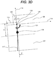
  • the shielding plate 108 , the sample 107 , and the sample stand 106 are in a swing direction 115 while having any angle on the left and right along with the swing axis 114 , but the beam center 116 of the ion beam 102 is set at a position perpendicular to the swing axis 114 . Therefore, the milling surface 117 of the sample is formed in a bilaterally symmetric Gaussian distribution shape along the end portion 118 of the shielding plate around a beam center 116 or a swing axis 114 .
  • the milling surface 117 is formed to be curved inwardly of the end portion 118 of the shielding plate in this way, when producing the central section of a fine structure 119 above or inside the sample, there is a possibility that an accurate central section may not be produced or the fine structure 119 itself may be scraped off.
  • FIG. 8 is a schematic plan view of a main part of an ion milling device illustrating another example of processing position adjustment of a sample, which is a view seen from the upper part of the shielding plate 108 , that is, a direction in which ions are heading to the sample 107 or the like.
  • the shielding plate 108 , the sample 107 , the sample stand 106 , and the sample stage 109 are disposed inside the vacuum chamber 104 .
  • the sample stand 106 is provided with a sample stand female thread portion 139 , and is connected to the sample stage 109 and the screw B 138 .
  • the shielding plate 108 when the shielding plate 108 is initially adjusted to the processing position A illustrated on the sample 107 , the energy of the ion beam 102 emitted from the ion source 101 is varied, and when the center of the ion beam 102 is changed to D on the sample 107 during processing of the sample 107 , when the processing position is intentionally adjusted by the user, or the like, the motor D 134 adjust the position of the sample stand 106 in the Y direction by being rotated counterclockwise to control the screw B 138 , and the motor E 142 adjust the position of the sample stage 109 in the X direction by being rotated counterclockwise to control the screw C 140 .
  • the sample and the shielding plate is tilted with respect to the ion beam irradiation direction as illustrated in FIG. 4B , and the section processing of the sample is performed, using the ion milling device having the configuration of FIG. 4A , a good sectional shape at a predetermined position can be obtained.
  • Embodiment 2 The ion milling device according to Embodiment 2 will be described with reference to FIG. 9 .
  • the matters described in Embodiment 1 and not described in the present embodiment can also be applied to the present embodiment as long as there is no particular circumstance.
  • FIG. 9 is a schematic sectional view of a main part of an ion milling device including an electrostatic deflection plate.
  • the shielding plate 108 and the sample 107 are disposed inside the vacuum chamber 104 .
  • An electrostatic deflection plate 127 is disposed in the ion source 101 , the ion beam 102 along the ion source center 126 is controlled by the ion source control unit 103 is curved by the electrostatic deflection plate (tilt unit) 127 , and the angle of the ion beam 102 to be applied to the sample 107 can be changed.
  • the electrostatic deflection plate can also be a deflection means using a magnetic field.
  • the irradiation angle ⁇ of the ion beam 102 is set to be greater than 0° and equal to or less than 10°, similarly to the sample tilt angle ⁇ in FIG. 4B .
  • the ion beam irradiation direction is tilted with respect to the sample and the shielding plate, and the section processing of the sample is performed, using the ion milling device having the configuration of FIG. 9 , a good sectional shape at a predetermined position can be obtained.
  • Embodiment 3 The ion milling device according to Embodiment 3 will be described with reference to FIG. 10 .
  • the matters described in Embodiment 1 or 2 and not described in the present embodiment can also be applied to the present embodiment as long as there is no particular circumstance.
  • FIG. 10 is a schematic sectional view of a main part of an ion milling device having a tilt mechanism of an ion source.
  • the shielding plate 108 , the sample 107 , the sample stand 106 , and the sample stage 109 are disposed inside the vacuum chamber 104 .
  • the ion beam irradiation direction is tilted with respect to the sample and the shielding plate, and the section processing of the sample is performed, using the ion milling device having the configuration of FIG. 10 , a good sectional shape at a predetermined position can be obtained.
  • the present invention includes the following embodiments.
  • a charged particle beam device including:
  • a shielding plate disposed such that a portion of the sample is exposed when seen from the ion source
  • a swing unit that swings the sample and the shielding plate around a swing axis which is orthogonal to a direction in which an end portion of the shielding plate on a side on which apart of the sample is exposed extends and intersects an ion beam from the ion source;
  • a tilt unit that relatively tilts the sample and the shielding plate by a tilt angle ⁇ with respect to the irradiation direction of the ion beam to the sample, in a direction in which the sample is shielded by the shielding plate, around a tilt axis which is set in the end portion of the shielding plate so as to be orthogonal to the swing axis and to intersect the ion beam.
  • the present invention is not limited to each of the above-described embodiments, and various modification examples are included.
  • the above-described embodiments have been described in detail in order to explain the present invention in an easy-to-understand manner and are not necessarily limited to those having all the configurations described.
  • some of the configurations of certain embodiments may be replaced with the configuration of the other embodiments, and it is also possible to add configurations of other embodiments to the configurations of certain embodiments.
  • addition, deletion, and replacement of another configuration can be performed.

Landscapes

  • Chemical & Material Sciences (AREA)
  • Analytical Chemistry (AREA)
  • Physics & Mathematics (AREA)
  • Engineering & Computer Science (AREA)
  • Plasma & Fusion (AREA)
  • Sampling And Sample Adjustment (AREA)
  • Analysing Materials By The Use Of Radiation (AREA)

Abstract

A charged particle beam device that can improve machining position precision in section processing using a shielding plate is provided. The invention is directed to a charged particle beam device including: an ion source (101); a sample stand (106) on which a sample (107) is mounted; a shielding plate (108) placed so that a portion of the sample (107) is exposed when seen from the ion source (101); and tilt units (123, 124) that tilt the sample (107) and the shielding plate (108) relative to the irradiation direction of an ion beam (102) from the ion source (101) to the sample (107).

Description

TECHNICAL FIELD
The present invention relates to a charged particle beam device.
BACKGROUND ART
An ion milling device which is one of charged particle beam devices is a sample pretreatment device such as a scanning electron microscope (SEM) or a transmission electron microscope (TEM), and is used as a device for manufacturing the section and plane of a sample in a wide range of fields. This is a device that irradiates a sample with accelerated argon ions and scrapes the sample using a sputtering phenomenon in which atoms of a sample fly from the surface of the sample, and generally there are a planar milling method and a section milling method.
The former planar milling method is a method of scraping a sample by directly irradiating a sample surface with ion beams that do not converge from an ion source, and has a feature that a wide range of the sample surface can be scraped off as described in PTL 1. On the other hand, in the latter section milling method, a shielding plate is disposed between an ion source and a sample, and the sample protrudes from the shielding plate by about several μm to 200 μm. Thus, it is possible to smoothly scrape the section of the sample along the end surface of the shielding plate by irradiating a part of the sample protruding from the shielding plate with the ion beam.
CITATION LIST Patent Literature
PTL 1: JP-A-3-36285
SUMMARY OF INVENTION Technical Problem
In recent years, there is a need to process materials with low sputtering yield such as ceramics and superhard materials in a wide range and in short time, and it is necessary to use an ion source corresponding to a high milling rate. Further, according to miniaturization of the sample, it is required to produce a wide section of a fine structure, and in general, a focused ion beam (FIB) is known as a section producing method for narrow samples, but it has difficulty in processing a wide area and needs much time for processing. Thus, a section milling method for producing section of a fine structure using a shielding plate is expected.
Then, the inventors have performed section ion milling on materials with low sputtering yield such as ceramics and superhard materials, by using an ion source of high energy (ions applied with a high acceleration voltage). As a result, it has been found that although the shielding plate is disposed at the intended position on the sample, the processed surface is formed in an overhang shape from the end surface of the shielding plate, for example, about several μm, and the sample processed surface along the end surface of the shielding plate cannot be obtained.
An object of the present invention is to provide a charged particle beam device that can improve processing position accuracy in section processing using a shielding plate.
Solution to Problem
As an embodiment to achieve the object, there is provided a charged particle beam device including: an ion source;
a sample stand on which a sample is placed; a shielding plate disposed such that a portion of the sample is exposed when seen from the ion source; and a tilt unit that relatively tilts the sample and the shielding plate in an irradiation direction of an ion beam from the ion source to the sample.
Advantageous Effects of Invention
According to the present invention, it is possible to provide a charged particle beam device capable of improving processing position accuracy in section processing using a shielding plate.
BRIEF DESCRIPTION OF DRAWINGS
FIG. 1 is a schematic diagram of an ion milling device according to Embodiment 1.
FIG. 2A is an image illustrating an example of Monte Carlo simulation of a scene in which a sample is irradiated with highly accelerated ion beams and the ion beams are scattered in the sample.
FIG. 2B is an image illustrating an example of Monte Carlo simulation of a scene in which a sample is irradiated with lowly accelerated ion beams and the ion beams are scattered in the sample.
FIG. 3A is a schematic bird's-eye view of a main part for explaining section ion milling of the sample.
FIG. 3B is a schematic sectional view of the sample illustrated in FIG. 3A, as viewed from the side.
FIG. 3C is a schematic sectional view of the sample when the sample is tilted and subjected to ion milling using the ion milling device illustrated in FIG. 1, as viewed from the side.
FIG. 3D is a schematic sectional view of the sample when a shielding plate is finely moved, and the sample is tilted and subjected to ion milling using the ion milling device illustrated in FIG. 1, as viewed from the side.
FIG. 4A is a schematic sectional view of a main part for explaining a tilt axis, in the ion milling device illustrated in FIG. 1.
FIG. 4B is a schematic sectional view (partial bird's-eye view) for explaining a tilt angle of the sample with respect to an irradiation direction of an ion beam.
FIG. 5 is a schematic overall sectional view of the ion milling device having a function of adjusting a processing position of the shielding plate and/or the sample according to Embodiment 1.
FIG. 6 is a schematic sectional view of a main part of the ion milling device illustrating an example of processing position adjustment of the shielding plate, according to Embodiment 1.
FIG. 7 is a schematic sectional view of a main part of the ion milling device illustrating an example of processing position adjustment of the sample, according to Embodiment 1.
FIG. 8 is a schematic plan view of a main part of the ion milling device illustrating another example of processing position adjustment of the sample, according to Embodiment 1.
FIG. 9 is a schematic sectional view of a main part of an ion milling device including an electrostatic deflection plate, according to Embodiment 2.
FIG. 10 is a schematic sectional view of a main part of an ion milling device having a tilt mechanism of an ion source, according to Embodiment 3.
DESCRIPTION OF EMBODIMENTS
The inventors have further studied the cause of the newly found deterioration of processing position accuracy. As a result, it has been found that the scattering of the ion beam to the inside of the sample is increased during the irradiation of the ion beam, the sample processed surface along the end surface of the shielding plate cannot be obtained due to formation of an amorphous layer and physical sputtering in a region shielded by the shielding plate.
The present invention has been made from this new knowledge, which makes it possible to perform flat processing along the end surface of the shielding plate, by adding a means for changing the incident angle of the sample, in consideration of the irradiation (incidence) angle of ions to be scattered in the inside of the sample in the vicinity of the end surface of the shielding plate that shields ion beams. In addition, it is possible to prevent the surface below the mask from being milled, by performing irradiation of ion beams while finely moving the shielding plate.
This makes it possible to avoid the influence of the sputtering phenomenon caused by the ions scattered in the inside of the sample on the processed surface, in the section ion milling using the shielding plate, and to obtain a smooth sample section along the end surface of the shielding plate, whereby the processing position accuracy of the device is improved.
Hereinafter, the present invention will be described in the following examples with reference to the drawings. Although an ion milling device will be described as a charged particle beam device, application to other apparatus using ions is also possible.
Embodiment 1
FIG. 1 illustrates the configuration of an ion milling device in which a shielding plate 108 is installed on the upper surface of a sample 107, the sample is irradiated with accelerated ion beams 102, and the cross section of a projecting portion of the sample is processed by utilizing a sputtering phenomenon of ions. The current density of argon ions in an argon ion source 101 is controlled by an ion source control unit 103. The interior of a vacuum chamber 104 can be evacuated or become an atmospheric state by controlling a vacuum evacuation system 105, and this state can be maintained.
The sample 107 is fixed on a sample stand 106. Further, when the interior of the vacuum chamber 104 is opened to the atmosphere, a sample stage 109 can be drawn out of the vacuum chamber 104. The sample stand 106 on which the sample 107 is fixed can be fixed on the sample stage 109. The sample 107 and the shielding plate 108 are independently fixed to be movable, and by irradiating the ion beam 102 emitted from the ion source 101, a part protruding from the shielding plate 108 of the sample 107 as seen from the ion source can be processed. The present ion milling device includes a tilt axis control section, a shielding plate fine movement mechanism, and the like which will be described later.
FIGS. 2A and 2B illustrate scattered ions 112 inside the sample 107 by Monte Carlo simulation when the sample 107 is irradiated with the argon ions 110 along an argon ion incidence direction 111. FIG. 2A illustrates a case where the sample 107 is irradiated with high acceleration ions and FIG. 2B illustrates a case of low acceleration ions. Here, it is understood that the scattering of ions inside the sample 107 is larger in FIG. 2A in which high acceleration ions are irradiated.
FIG. 3A is a schematic bird's-eye view of a main part for explaining section ion milling of the sample, and FIG. 3B is a schematic cross-sectional view of the sample illustrated in FIG. 3A, as viewed from the side. As illustrated in FIG. 3A, in the section milling, the user presets a protrusion amount 113 of the sample 107 from the shielding plate 108 before processing, and the sample 107 is irradiated with the ion beams 102. For convenience, the protrusion amount 113 is demonstrated larger in comparison with the thickness of the shielding plate 108. In this case, the shielding plate 108, the sample 107, and the sample stand 106 are in a swing direction 115 while having any angle on the left and right along with the swing axis 114, but the beam center 116 of the ion beam 102 is set at a position perpendicular to the swing axis 114. Therefore, the milling surface 117 of the sample is formed in a bilaterally symmetric Gaussian distribution shape along the end portion 118 of the shielding plate around a beam center 116 or a swing axis 114.
However, in the section processing performed in the related art, as illustrated in FIG. 3B, the ion beam 102 is scattered inside the sample 107, and the milling surface 117 is not formed perpendicular to the shielding plate 108. In the irradiation of high acceleration ions as illustrated in FIGS. 2A and 2B, the amount of scattered ions 112 inside the sample 107 increases and enters the lower portion of the shielding plate, so the milling surface 117 becomes more curved.
For example, when the protrusion amount 113 of the sample 107 from the shielding plate 108 is set to about 50 μm, and the sample 107 is irradiated with the ion beam 102 with the acceleration voltage of 6 kV, as illustrated in FIG. 3B, the milling surface 117 is formed inside the end portion 118 of the shielding plate by the maximum β (about 5 μm) at the lower portion of the contact surface of the shielding plate 108 and the upper part of the sample 107 by α (about 400 μm). If the milling surface 117 is formed to be curved inwardly of the end portion 118 of the shielding plate in this way, when producing the central section of a fine structure 119 above or inside the sample, there is a possibility that an accurate central section may not be produced or the fine structure 119 itself may be scraped off. There is also a method of processing the sample 107 by setting the acceleration voltage of the ion beam 102 at a low acceleration, but the processing time becomes longer.
Therefore, in the present embodiment, as illustrated in FIG. 3C, since the tilt axis 120 is provided along the end portion 118 of the shielding plate to change the angle of the ion beam 102 entering the sample 107, It is possible to form the milling surface 117 perpendicular to the shielding plate 108 in a short time using the high acceleration ion beam 102. At this time, the sample, the shielding plate and the like are tilted in a direction in which the sample is masked by the shielding plate with respect to the ion beam around the tilt axis. Reference numeral 121 denotes a tilt driving direction.
On the other hand, in the ion milling device, the ion beam 102 emitted from the ion source 101 spreads broadly without being subjected to the converging action and is applied to the sample 107. However, when the acceleration voltage of the ion beam 102 is changed, the position of the beam center 116 is changed, and it is difficult to control the beam center 116 perpendicularly to the swing axis 114, such as in the case where the acceleration voltage is changed during processing. Generally, the beam center 116 of the ion beam 102 has the highest ion density, and the processing speed is highest at the position of the sample 107 processed at the beam center 116. However, when the beam center 116 changes as described above, a problem of prolonged processing time due to a decrease in a processing speed occurs.
Therefore, as illustrated in FIG. 3D, by providing a mechanism capable of fine movement 122 of the shielding plate according to the acceleration voltage of the ion beam 102, the beam center 116 is always set at the end portion 118 of the shielding plate, and thus it is possible to solve the above-described problem. Reference numeral 121 denotes a tilt driving direction.
FIG. 4A is a schematic sectional view of a main part for explaining a tilt axis, in the ion milling device illustrated in FIG. 1. The shielding plate 108, the sample 107, the sample stand 106, and the sample stage 109 are disposed inside the vacuum chamber 104, the sample stage 109 is connected to the motor A (a part of the tilt unit) 124 disposed outside the vacuum chamber 104, and the motor A 124 is connected to a tilt control unit (a part of the tilt unit) 123. Further, the sample 107 is irradiated with the ion beam 102 emitted from the ion source 101, and the milling surface 117 having a Gaussian distribution is formed on the sample 107.
Any angle is set by the tilt control unit 123, and by operating the motor A 124, the sample stage 109 on which the shielding plate 108, the sample 107, and the sample stand 106 are placed is tilted around the rotation center axis 125 of the motor A, that is, the tilt axis 120. By tilting the sample 107 as described above, the incident angle of the ion beam 102 applied to the sample 107 is changed. In the present embodiment, the tilt angle is variable using the motor A or the like, but a tilt unit can also be formed using a member that can be fixed at a predetermined tilt angle.
FIG. 4B is a schematic diagram in a case where the sample 107 and the shielding plate 108 are tilted using the tilt axis 120. At this time, the sample, the shielding plate and the like are tilted in a direction in which the sample is masked by the shielding plate with respect to the tilt axis set at the end of the shielding plate so as to intersect with the ion beam and be orthogonal to the swing axis. That is, by setting the sample tilt angle θ on the side of the shielding plate 108 with respect to the ion source center 126, it is possible to reduce the scattered ions 112 inside the sample 107 immediately below the shielding plate 108. Therefore, the problem that the milling surface 117 illustrated in FIG. 3B is not formed perpendicular to the shielding plate 108 can be solved. It is desirable that the sample tilt angle θ is set to be greater than 0° and equal to or less than 10°. The value β can be reduced by setting the tilt angle to be greater than 0°, and a section at a desired position can be obtained by setting the tilt angle to be equal to or less than 10°.
FIG. 5 is a schematic overall sectional view of an ion milling device having a function of adjusting a processing position of a shielding plate and/or a sample. The interior of the vacuum chamber 104 is maintained in a vacuum state by the vacuum evacuation system 105, and is in a state where the ion beam 102 can be emitted from the ion source 101 at any time by the ion source control unit 103. Further, the shielding plate 108, the sample 107, the sample stand 106, and the sample stage 109 are disposed inside the vacuum chamber 104, and a signal is transmitted from the ion source control unit 103 to the shielding plate and/or sample stand fine movement mechanism control unit 135. The motor C 133 is operated under the control of the shielding plate and/or sample stand fine movement mechanism control unit 135, and the position of the shielding plate 108 can be controlled from the outside of the vacuum chamber 104.
Similarly, the motor D 134 is operated under the control of the shielding plate and/or the sample stand fine movement mechanism control unit 135, and the position of the sample stand 106 can be controlled from outside the vacuum chamber 104. From this, the energy of the ion beam 102 emitted from the ion source 101 and the positions of the shielding plate 108 and the sample stand 106 are controlled from outside the vacuum chamber 104 by the user, according to the acceleration voltage instructed by the ion source control unit 103.
At this time, for example, in the shielding plate and/or sample stand fine movement mechanism control unit 135, the relationship between the energy of the ion beam previously stored in the internal memory 160 and the position of the sample stand with respect to the shielding plate is used, and the installation position of the shielding plate with respect to the sample is automatically controlled. The memory 160 may be provided outside the shielding plate and/or sample stand fine movement mechanism control unit 135. Alternatively, it is possible to adjust the installation position of the shielding plate with respect to the sample accurately and manually, by adjusting the positions of the shielding plate 108 and/or the sample stand 106 based on information obtained by a camera, a microscope, or a monitor installed in a vacuum chamber, or a mechanism combining them.
FIG. 6 is a schematic sectional view of a main part of an ion milling device illustrating an example of processing position adjustment of the shielding plate. The shielding plate 108, the sample 107, the sample stand 106, and the sample stage 109 are disposed inside the vacuum chamber 104. Further, a shielding plate female thread portion 137 is provided on the shielding plate 108, and is connected to the sample stage 109 and a screw A 136. The position of the shielding plate 108 can be controlled, by a motor C 133 being operated under the control of a shielding plate and/or sample stand fine movement mechanism control unit 135 and the screw A 136 being rotated.
For example, when the shielding plate 108 is initially adjusted to the processing position A illustrated on the sample 107, the energy of the ion beam 102 emitted from the ion source 101 is varied, and when the center of the ion beam 102 is changed to B on the sample 107 during processing of the sample 107, when the processing position is intentionally adjusted by the user, or the like, the motor C 133 adjusts the position of the shielding plate 108 by being rotated clockwise to control the screw A 136.
For the same reason as above, when the center of the ion beam 102 is changed to C on the sample during processing of the sample 107, when the processing position is intentionally adjusted by the user, or the like, the motor C 133 adjusts the position of the shielding plate 108 by being rotated counterclockwise to control the screw A 136. Further, it is possible to precisely adjust the positions of the shielding plate 108 and the sample stand 106, using a camera, a microscope, or a monitor installed in a vacuum chamber, or a mechanism combining them.
FIG. 7 is a schematic sectional view of a main part of an ion milling device illustrating an example of processing position adjustment of a sample. The shielding plate 108, the sample 107, the sample stand 106, and the sample stage 109 are disposed inside the vacuum chamber 104. Further, the sample stand 106 is provided with a sample stand female thread portion 139, and is connected to the sample stage 109 and a screw B 138. The motor D 134 is operated under the control of the shielding plate and/or sample stand fine movement mechanism control unit 135, and the position of the sample stand 106 can be controlled by the screw B 138 being rotated.
For example, when the shielding plate 108 is initially adjusted to the processing position A illustrated on the sample 107, the energy of the ion beam 102 emitted from the ion source 101 is varied, and when the center of the ion beam 102 is changed to B on the sample 107 during processing of the sample 107, when the processing position is intentionally adjusted by the user, or the like, the motor D 134 adjusts the position of the sample stand 106 by being rotated clockwise to control the screw B 138. For the same reason as above, when the center of the ion beam 102 is changed to C on the sample 107 during processing of the sample 107, when the processing position is intentionally adjusted by the user, or the like, the motor D 134 rotates counterclockwise to control the screw B and adjust the position of the sample stand 106. Further, it is possible to precisely adjust the positions of the shielding plate 108 and the sample stand 106, using a camera, a microscope, or a monitor installed in a vacuum chamber, or a mechanism combining them.
FIG. 8 is a schematic plan view of a main part of an ion milling device illustrating another example of processing position adjustment of a sample, which is a view seen from the upper part of the shielding plate 108, that is, a direction in which ions are heading to the sample 107 or the like. The shielding plate 108, the sample 107, the sample stand 106, and the sample stage 109 are disposed inside the vacuum chamber 104. The sample stand 106 is provided with a sample stand female thread portion 139, and is connected to the sample stage 109 and the screw B 138.
On the other hand, the sample stage 109 is provided with a sample stage female threaded portion 141 and is connected to a screw C 140. The motor D and motor E control unit 143 is connected to the motor D 134 and the motor E 142; rotates the screw C 140 using the motor E 142 and operates the sample stage 109 when the processing position is adjusted in the X direction in response to the instruction of the motor D and motor E control unit 143; and rotates the screw B 138 using the motor D 134 and operates the sample stand 106 in a case of adjusting the processing position in the Y direction, whereby it is possible to freely adjust the processing position in the XY direction.
For example, when the shielding plate 108 is initially adjusted to the processing position A illustrated on the sample 107, the energy of the ion beam 102 emitted from the ion source 101 is varied, and when the center of the ion beam 102 is changed to D on the sample 107 during processing of the sample 107, when the processing position is intentionally adjusted by the user, or the like, the motor D 134 adjust the position of the sample stand 106 in the Y direction by being rotated counterclockwise to control the screw B 138, and the motor E 142 adjust the position of the sample stage 109 in the X direction by being rotated counterclockwise to control the screw C 140. Here, it is also possible to perform XY adjustment of the processing position by reversing the adjustment mechanism in the X direction and the Y direction provided on the sample stand 106 and the sample stage 109. Further, it is possible to precisely adjust the positions of the shielding plate 108 and the sample stand 106, using a camera, a microscope, or a monitor installed in a vacuum chamber, or a mechanism combining them.
when a ceramic, a superhard material, or the like is used as a sample, the sample and the shielding plate is tilted with respect to the ion beam irradiation direction as illustrated in FIG. 4B, and the section processing of the sample is performed, using the ion milling device having the configuration of FIG. 4A, a good sectional shape at a predetermined position can be obtained.
As described above, according to the present embodiment, it is possible to provide a charged particle beam device capable of improving processing position accuracy even with a material with low sputtering yield, in the section processing using the shielding plate, by providing the tilt unit that relatively tilts the sample and the shielding plate with respect to the irradiation direction of the ion beam to the sample. Further, it is possible to further improve the processing position accuracy, by making the angle of tilting variable. Further, it is possible to further improve the processing position accuracy, by providing the fine movement mechanism of a shielding plate and/or a sample.
Embodiment 2
The ion milling device according to Embodiment 2 will be described with reference to FIG. 9. The matters described in Embodiment 1 and not described in the present embodiment can also be applied to the present embodiment as long as there is no particular circumstance.
FIG. 9 is a schematic sectional view of a main part of an ion milling device including an electrostatic deflection plate. The shielding plate 108 and the sample 107 are disposed inside the vacuum chamber 104. An electrostatic deflection plate 127 is disposed in the ion source 101, the ion beam 102 along the ion source center 126 is controlled by the ion source control unit 103 is curved by the electrostatic deflection plate (tilt unit) 127, and the angle of the ion beam 102 to be applied to the sample 107 can be changed. The electrostatic deflection plate can also be a deflection means using a magnetic field.
Here, as illustrated in FIG. 4B, by setting the irradiation angle θ of the ion beam 102 on the side of the shielding plate 108 with respect to the ion source center 126, it is possible to reduce the scattered ions 112 inside the sample 107 immediately below the shielding plate 108, similar to the case where the tilt axis 120 is provided at the end portion 118 of the shielding plate illustrated in FIG. 4A and the sample 107 is tilted. Therefore, the problem that the milling surface 117 illustrated in FIG. 3B is not formed perpendicular to the shielding plate 108 can be solved. Here, it is desirable that the irradiation angle θ′ of the ion beam 102 is set to be greater than 0° and equal to or less than 10°, similarly to the sample tilt angle θ in FIG. 4B.
when a ceramic, a superhard material, or the like is used as a sample, the ion beam irradiation direction is tilted with respect to the sample and the shielding plate, and the section processing of the sample is performed, using the ion milling device having the configuration of FIG. 9, a good sectional shape at a predetermined position can be obtained.
As described above, according to the present embodiment, it is possible to obtain the same effect as in Embodiment 1.
Embodiment 3
The ion milling device according to Embodiment 3 will be described with reference to FIG. 10. The matters described in Embodiment 1 or 2 and not described in the present embodiment can also be applied to the present embodiment as long as there is no particular circumstance.
FIG. 10 is a schematic sectional view of a main part of an ion milling device having a tilt mechanism of an ion source. The shielding plate 108, the sample 107, the sample stand 106, and the sample stage 109 are disposed inside the vacuum chamber 104. Further, the ion source 101 is connected to a worm gear (a part of the tilt unit) 130 through an arm (a part of the tilt unit) 131, and is constituted to be interlocked with a motor B (a part of the tilt unit) 128 controlled by the motor B control unit (a part of the tilt unit) 146 The motor B control unit 146 sets the angle to an any angle, and the ion source 101 or the ion source center 126 is tilted around the motor B rotation center axis 129, through the motor B 128, the worm gear 130, and the arm 131, as illustrated in an ion source driving direction 132. In this way, similar to the case illustrated in FIG. 9, in the ion source 101, by setting the irradiation angle θ greater than 0° and equal to or less than 10° on the side of the shielding plate 108, the problem that the milling surface 117 illustrated in FIG. 3B is not formed perpendicular to the shielding plate 108 can be solved.
when a ceramic, a superhard material, or the like is used as a sample, the ion beam irradiation direction is tilted with respect to the sample and the shielding plate, and the section processing of the sample is performed, using the ion milling device having the configuration of FIG. 10, a good sectional shape at a predetermined position can be obtained.
As described above, according to the present embodiment, it is possible to obtain the same effect as in Embodiment 1.
The present invention includes the following embodiments.
A charged particle beam device including:
an ion source;
a sample stand on which a sample is placed;
a shielding plate disposed such that a portion of the sample is exposed when seen from the ion source;
a swing unit that swings the sample and the shielding plate around a swing axis which is orthogonal to a direction in which an end portion of the shielding plate on a side on which apart of the sample is exposed extends and intersects an ion beam from the ion source; and
a tilt unit that relatively tilts the sample and the shielding plate by a tilt angle θ with respect to the irradiation direction of the ion beam to the sample, in a direction in which the sample is shielded by the shielding plate, around a tilt axis which is set in the end portion of the shielding plate so as to be orthogonal to the swing axis and to intersect the ion beam.
It should be noted that the present invention is not limited to each of the above-described embodiments, and various modification examples are included. For example, the above-described embodiments have been described in detail in order to explain the present invention in an easy-to-understand manner and are not necessarily limited to those having all the configurations described. In addition, some of the configurations of certain embodiments may be replaced with the configuration of the other embodiments, and it is also possible to add configurations of other embodiments to the configurations of certain embodiments. Further, with respect to a part of the configuration of each of the embodiments, addition, deletion, and replacement of another configuration can be performed.
REFERENCE SIGNS LIST
    • 101: ion source
    • 102: ion beam
    • 103: ion source control unit
    • 104: vacuum chamber
    • 105: vacuum evacuation system
    • 106: sample stand
    • 107: sample
    • 108: shielding plate
    • 109: sample stage
    • 110: argon ion
    • 111: argon ion incident direction
    • 112: scattered ion
    • 113: protrusion amount
    • 114: swing axis
    • 115: swing (direction)
    • 116: beam center
    • 117: milling surface
    • 118: end portion of shielding plate
    • 119: fine structure
    • 120: tilt axis
    • 121: tilt driving direction
    • 122: fine movement of shielding plate
    • 123: tilt control unit
    • 124: motor A (part of tilt unit)
    • 125: motor A rotation center axis
    • 126: ion source center
    • 127: electrostatic deflection plate
    • 128: motor B (part of tilt unit)
    • 129: motor B rotation center axis
    • 130: worm gear (part of tilt unit)
    • 131: arm (part of tilt unit)
    • 132: ion source driving direction
    • 133: motor C
    • 134: motor D
    • 135: shielding plate and/or sample stand fine movement mechanism control unit
    • 136: screw A
    • 137: shielding plate female thread portion
    • 138: screw B
    • 139: sample stand female thread portion
    • 140: screw C
    • 141: sample stage female thread portion
    • 142: motor E
    • 143: control units of motor D and motor E
    • 146: control unit of motor B
    • 160: memory

Claims (11)

The invention claimed is:
1. A charged particle beam device comprising:
an ion source adapted to generate an ion beam having an ion beam center;
a sample stage on which a sample is placed for section milling a section surface of the sample, using the ion beam;
a shielding plate that is disposed on the sample stage between the ion source and the sample such that a portion protrusion amount of the sample is exposed to the ion beam for section milling of the protrusion amount of the sample, when that protrusion amount of the sample extends beyond an end portion of the shielding plate and is seen from the ion source;
a sample movement mechanism and a shielding plate movement mechanism, whereby the sample and the shielding plate are movable independently with respect to each other, the sample movement mechanism and the shielding plate movement mechanism including a fine movement control unit that finely moves the shielding plate respective to the sample stand such that an exposure amount of the sample can be finely adjusted, as viewed from the ion source, in accordance with an accelerator voltage of the ion beam;
a sample stage tilt unit, which sample stage tilt unit tilts the sample and the shielding plate about a tilt angle θ, around a tilt axis, which tilt axis is orthogonal to, and which intersects the ion beam from the ion source at a point of contact between the protrusion amount of the sample and the end portion of the shielding plate, which tilt axis extends in a direction whereby, on rotation of the sample stage about the tilt axis, the end portion of the shielding plate, from which end portion of the shielding plate the protrusion amount of the sample extends, masks a part of the protrusion amount of the sample extending beyond the end portion of the shielding plate, with respect to the ion beam;
a swing unit that swings the sample and the shielding plate around a swing axis, which swing axis is orthogonal to the tilt axis and intersects the ion beam; and
whereby, the provision of the tilt axis at the end portion of the shielding plate using the fine movement control unit allows a change in the tilt angle ⊖, to change an angle of the ion beam entering the sample, to form a milling surface in the sample which milling surface is perpendicular to the shielding plate.
2. The charged particle beam device according to claim 1, wherein
the tilt unit includes a mechanical mechanism that varies the tilt angle θ relative to an irradiation direction of the ion beam to the sample.
3. The charged particle beam device according to claim 2, wherein
the tilt angle is variable on a side of the shielding plate with respect to the irradiation direction of the ion beam to the sample in a range between 0° and 10°.
4. The charged particle beam device according to claim 2, wherein
the mechanical mechanism further includes a tilt mechanism that tilts the ion source.
5. The charged particle beam device according to claim 2, wherein
the mechanical mechanism further includes a tilt mechanism that tilts a sample stage on which the sample stand is installed.
6. The charged particle beam device according to claim 1, wherein
the sample stand tilt unit further includes an ion beam deflecting plate that varies the tilt angle θ relative to the irradiation direction of the ion beam to the sample.
7. The charged particle beam device according to claim 6, wherein
the tilt angle θ is variable on a side of the shielding plate with respect to the irradiation direction of the ion beam to the sample in a range between 0° and 10°.
8. The charged particle beam device according to claim 1, wherein
the fine movement mechanism is controlled using a relationship between the energy of the ion beam and a position of the sample stand with respect to the shielding plate, which relationship is stored in advance.
9. The charged particle beam device according to claim 1, wherein
the fine movement mechanism is manually adjustable, based on information obtained by one of a camera, a microscope, a monitor, and a combination thereof.
10. A charged particle beam device comprising:
an ion source adapted to generate an ion beam having an ion beam center;
a sample stand on which a sample is placed for section milling a section surface of the sample using the ion beam;
a shielding plate that is disposed between the ion source and the sample such that a protrusion amount of the sample is exposed to the ion beam for section milling of the protrusion amount of the sample when that exposed protrusion amount of the sample is seen from the ion source;
a sample movement mechanism and a shielding plate movement mechanism, whereby the sample and the shielding plate are movable independently with respect to each other, the sample movement mechanism and the shielding plate movement mechanism including a fine movement control unit that finely moves the shielding plate respective to the sample stand such that an exposure amount of the sample can be finely adjusted, as viewed from the ion source, in accordance with an accelerator voltage of the ion beam;
a swing unit that swings the sample and the shielding plate around a swing axis which swing axis is orthogonal to a direction in which an end portion of the shielding plate, on a side of which end portion a part of the sample is exposed, extends and intersects the ion beam from the ion source;
a sample stage tilt unit, which sample stage tilt unit tilts the sample and the shielding plate about a tilt angle θ, around a tilt axis, which tilt axis is orthogonal to, and which is set in a direction in which the end portion of the shielding plate extends so as to be orthogonal to the swing axis and to intersect the ion beam, in a direction in which a part of the protrusion amount the sample, extending beyond the end face of the shielding plate, is masked by the shielding plate with respect to an irradiation direction of the ion beam to the sample; and
whereby, the provision of the tilt axis at the end portion of the shielding plate using the fine movement control unit allows a change in the tilt angle ⊖, to change an angle of the ion beam entering the sample, to form a milling surface in the sample which milling surface is perpendicular to the shielding plate.
11. The charged particle beam device according to claim 10, wherein
the tilt angle θ is variable in a range of between 0° and 10°.
US16/320,525 2016-08-09 2016-08-09 Charged particle beam device Active US10832889B2 (en)

Applications Claiming Priority (1)

Application Number Priority Date Filing Date Title
PCT/JP2016/073414 WO2018029778A1 (en) 2016-08-09 2016-08-09 Charged particle beam device

Publications (2)

Publication Number Publication Date
US20190272973A1 US20190272973A1 (en) 2019-09-05
US10832889B2 true US10832889B2 (en) 2020-11-10

Family

ID=61161837

Family Applications (1)

Application Number Title Priority Date Filing Date
US16/320,525 Active US10832889B2 (en) 2016-08-09 2016-08-09 Charged particle beam device

Country Status (5)

Country Link
US (1) US10832889B2 (en)
JP (1) JP6727307B2 (en)
KR (1) KR102188382B1 (en)
CN (1) CN109478488B (en)
WO (1) WO2018029778A1 (en)

Families Citing this family (3)

* Cited by examiner, † Cited by third party
Publication number Priority date Publication date Assignee Title
JP7280983B2 (en) 2020-01-29 2023-05-24 株式会社日立ハイテク Ion milling device
JP7208195B2 (en) 2020-08-14 2023-01-18 日本電子株式会社 Ion milling device and sample holder
JP7797007B2 (en) * 2022-04-22 2026-01-13 株式会社ブイ・テクノロジー Reflective mask blank manufacturing method, reflective mask blank, and focused ion beam processing apparatus

Citations (9)

* Cited by examiner, † Cited by third party
Publication number Priority date Publication date Assignee Title
JPH0336285A (en) 1989-07-01 1991-02-15 Hitachi Nakaseiki Ltd Ion milling device
JP2004071486A (en) 2002-08-09 2004-03-04 Seiko Instruments Inc Focused charged particle beam device
US20050116182A1 (en) * 2003-11-27 2005-06-02 Maki Tanaka Method of measuring pattern dimension and method of controlling semiconductor device process
WO2011130100A2 (en) 2010-04-11 2011-10-20 Steven Thomas Coyle Ion beam sample preparation apparatus and methods
JP2012018164A (en) 2010-07-06 2012-01-26 Kamtec Ltd Method and system for preparing lamella
WO2012060416A1 (en) 2010-11-05 2012-05-10 株式会社 日立ハイテクノロジーズ Ion milling device
KR20130086046A (en) 2010-11-22 2013-07-30 가부시키가이샤 히다치 하이테크놀로지즈 Ion milling device and ion milling processing method
US20150228446A1 (en) * 2014-02-11 2015-08-13 Infineon Technologies Ag Implantation Apparatus with Ion Beam Directing Unit, Semiconductor Device and Method of Manufacturing
US20170047198A1 (en) * 2014-05-09 2017-02-16 Hitachi High- Technologies Corporation Ion Milling Apparatus and Sample Processing Method

Family Cites Families (7)

* Cited by examiner, † Cited by third party
Publication number Priority date Publication date Assignee Title
KR20120098627A (en) * 2009-09-18 2012-09-05 마퍼 리쏘그라피 아이피 비.브이. Charged particle optical system with multiple beams
US8653489B2 (en) * 2010-04-11 2014-02-18 Gatan, Inc. Ion beam sample preparation apparatus and methods
EP2656369B8 (en) * 2010-12-22 2016-09-21 Excillum AB Aligning and focusing an electron beam in an x-ray source
EP2525385A1 (en) * 2011-05-16 2012-11-21 Fei Company Charged-particle microscope
WO2014192361A1 (en) * 2013-05-30 2014-12-04 株式会社 日立ハイテクノロジーズ Charged-particle-beam device and specimen observation method
WO2015030271A1 (en) * 2013-08-28 2015-03-05 한국기초과학지원연구원 Sample stage for multipurpose three-dimensional imaging and precision control device of sample holder in transmission electron microscope
JP6383650B2 (en) * 2014-11-28 2018-08-29 株式会社日立ハイテクノロジーズ Charged particle beam equipment

Patent Citations (17)

* Cited by examiner, † Cited by third party
Publication number Priority date Publication date Assignee Title
JPH0336285A (en) 1989-07-01 1991-02-15 Hitachi Nakaseiki Ltd Ion milling device
JP2004071486A (en) 2002-08-09 2004-03-04 Seiko Instruments Inc Focused charged particle beam device
US20050035306A1 (en) 2002-08-09 2005-02-17 Kouji Iwasaki Focused charged particle beam apparatus
US20050116182A1 (en) * 2003-11-27 2005-06-02 Maki Tanaka Method of measuring pattern dimension and method of controlling semiconductor device process
US20130228702A1 (en) * 2010-04-11 2013-09-05 Gatan, Inc. Ion Beam Sample Preparation Apparatus and Methods
US20120085939A1 (en) * 2010-04-11 2012-04-12 Gatan, Inc. Ion Beam Sample Preparation Apparatus and Methods
JP2013527435A (en) 2010-04-11 2013-06-27 ガタン インコーポレイテッド Ion beam sample preparation apparatus and method
WO2011130100A2 (en) 2010-04-11 2011-10-20 Steven Thomas Coyle Ion beam sample preparation apparatus and methods
JP2012018164A (en) 2010-07-06 2012-01-26 Kamtec Ltd Method and system for preparing lamella
US20120080406A1 (en) 2010-07-06 2012-04-05 Camtek Ltd. Method and system for preparing a lamela
WO2012060416A1 (en) 2010-11-05 2012-05-10 株式会社 日立ハイテクノロジーズ Ion milling device
US20130220806A1 (en) * 2010-11-05 2013-08-29 Hitachi High-Technologies Corporation Ion milling device
US20160163508A1 (en) * 2010-11-05 2016-06-09 Hitachi High-Technologies Corporation Ion milling device
KR20130086046A (en) 2010-11-22 2013-07-30 가부시키가이샤 히다치 하이테크놀로지즈 Ion milling device and ion milling processing method
US20130240353A1 (en) * 2010-11-22 2013-09-19 Hitachi High-Technologies Corporation Ion milling device and ion milling processing method
US20150228446A1 (en) * 2014-02-11 2015-08-13 Infineon Technologies Ag Implantation Apparatus with Ion Beam Directing Unit, Semiconductor Device and Method of Manufacturing
US20170047198A1 (en) * 2014-05-09 2017-02-16 Hitachi High- Technologies Corporation Ion Milling Apparatus and Sample Processing Method

Non-Patent Citations (2)

* Cited by examiner, † Cited by third party
Title
International Search Report of PCT/JP2016/073414 dated Oct. 25, 2016.
Korean Office Action received in corresponding Korean Application No. 10-2019-7002085 dated Jul. 8, 2020.

Also Published As

Publication number Publication date
KR20190020790A (en) 2019-03-04
US20190272973A1 (en) 2019-09-05
WO2018029778A1 (en) 2018-02-15
JPWO2018029778A1 (en) 2019-06-06
CN109478488B (en) 2021-01-08
KR102188382B1 (en) 2020-12-08
JP6727307B2 (en) 2020-07-22
CN109478488A (en) 2019-03-15

Similar Documents

Publication Publication Date Title
EP0824759B1 (en) Ion beam preparation device for electron microscopy
US9499900B2 (en) Ion milling device
JP2753306B2 (en) Ion beam processing method and focused ion beam device
US8835846B2 (en) Imaging a sample in a TEM equipped with a phase plate
US20160071693A1 (en) Control of ion angular distribution of ion beams with hidden deflection electrode
US10832889B2 (en) Charged particle beam device
WO2005003736A1 (en) Thin piece specimen preparing method and composite charged particle beam device
US10600612B2 (en) Charged particle beam apparatus
WO2001067501A1 (en) Apparatus and method for reducing differential sputter rates
JP6207081B2 (en) Focused ion beam device
US20190189388A1 (en) Composite beam apparatus
WO2012005232A1 (en) Charged particle beam device and sample production method
KR20180111579A (en) Electron-beam irradiation apparatus and dynamic focus adjusting method of electron-beam
EP2036112A2 (en) Apparatus for accelerating an ion beam
JP7554542B2 (en) Focused Ion Beam Equipment
TWI766500B (en) Ion Milling Device
US9773638B2 (en) Specimen preparation device
US10832918B2 (en) Method for removal of matter
JP2011243540A (en) Selected area aperture plate of transmission electron microscope, manufacturing method of selected area aperture plate, and observing method of selected area electron diffraction image
WO2019185069A1 (en) A device for creating and placing a lamella
JP2023091280A (en) Sample processing device and sample processing method

Legal Events

Date Code Title Description
AS Assignment

Owner name: HITACHI HIGH-TECHNOLOGIES CORPORATION, JAPAN

Free format text: ASSIGNMENT OF ASSIGNORS INTEREST;ASSIGNORS:KANEKO, ASAKO;TAKASU, HISAYUKI;IWAYA, TORU;SIGNING DATES FROM 20181205 TO 20181207;REEL/FRAME:048132/0478

FEPP Fee payment procedure

Free format text: ENTITY STATUS SET TO UNDISCOUNTED (ORIGINAL EVENT CODE: BIG.); ENTITY STATUS OF PATENT OWNER: LARGE ENTITY

STPP Information on status: patent application and granting procedure in general

Free format text: DOCKETED NEW CASE - READY FOR EXAMINATION

STPP Information on status: patent application and granting procedure in general

Free format text: NON FINAL ACTION MAILED

STPP Information on status: patent application and granting procedure in general

Free format text: RESPONSE TO NON-FINAL OFFICE ACTION ENTERED AND FORWARDED TO EXAMINER

AS Assignment

Owner name: HITACHI HIGH-TECH CORPORATION, JAPAN

Free format text: CHANGE OF NAME AND ADDRESS;ASSIGNOR:HITACHI HIGH-TECHNOLOGIES CORPORATION;REEL/FRAME:052259/0227

Effective date: 20200212

STPP Information on status: patent application and granting procedure in general

Free format text: NOTICE OF ALLOWANCE MAILED -- APPLICATION RECEIVED IN OFFICE OF PUBLICATIONS

STPP Information on status: patent application and granting procedure in general

Free format text: PUBLICATIONS -- ISSUE FEE PAYMENT VERIFIED

STCF Information on status: patent grant

Free format text: PATENTED CASE

MAFP Maintenance fee payment

Free format text: PAYMENT OF MAINTENANCE FEE, 4TH YEAR, LARGE ENTITY (ORIGINAL EVENT CODE: M1551); ENTITY STATUS OF PATENT OWNER: LARGE ENTITY

Year of fee payment: 4