US10831069B2 - Display device - Google Patents
Display device Download PDFInfo
- Publication number
- US10831069B2 US10831069B2 US15/947,324 US201815947324A US10831069B2 US 10831069 B2 US10831069 B2 US 10831069B2 US 201815947324 A US201815947324 A US 201815947324A US 10831069 B2 US10831069 B2 US 10831069B2
- Authority
- US
- United States
- Prior art keywords
- spacer
- substrate
- signal lines
- display device
- substrate sub
- Prior art date
- Legal status (The legal status is an assumption and is not a legal conclusion. Google has not performed a legal analysis and makes no representation as to the accuracy of the status listed.)
- Active, expires
Links
Images


Classifications
-
- G—PHYSICS
- G02—OPTICS
- G02F—OPTICAL DEVICES OR ARRANGEMENTS FOR THE CONTROL OF LIGHT BY MODIFICATION OF THE OPTICAL PROPERTIES OF THE MEDIA OF THE ELEMENTS INVOLVED THEREIN; NON-LINEAR OPTICS; FREQUENCY-CHANGING OF LIGHT; OPTICAL LOGIC ELEMENTS; OPTICAL ANALOGUE/DIGITAL CONVERTERS
- G02F1/00—Devices or arrangements for the control of the intensity, colour, phase, polarisation or direction of light arriving from an independent light source, e.g. switching, gating or modulating; Non-linear optics
- G02F1/01—Devices or arrangements for the control of the intensity, colour, phase, polarisation or direction of light arriving from an independent light source, e.g. switching, gating or modulating; Non-linear optics for the control of the intensity, phase, polarisation or colour
- G02F1/13—Devices or arrangements for the control of the intensity, colour, phase, polarisation or direction of light arriving from an independent light source, e.g. switching, gating or modulating; Non-linear optics for the control of the intensity, phase, polarisation or colour based on liquid crystals, e.g. single liquid crystal display cells
- G02F1/133—Constructional arrangements; Operation of liquid crystal cells; Circuit arrangements
- G02F1/1333—Constructional arrangements; Manufacturing methods
- G02F1/1339—Gaskets; Spacers; Sealing of cells
-
- G—PHYSICS
- G02—OPTICS
- G02F—OPTICAL DEVICES OR ARRANGEMENTS FOR THE CONTROL OF LIGHT BY MODIFICATION OF THE OPTICAL PROPERTIES OF THE MEDIA OF THE ELEMENTS INVOLVED THEREIN; NON-LINEAR OPTICS; FREQUENCY-CHANGING OF LIGHT; OPTICAL LOGIC ELEMENTS; OPTICAL ANALOGUE/DIGITAL CONVERTERS
- G02F1/00—Devices or arrangements for the control of the intensity, colour, phase, polarisation or direction of light arriving from an independent light source, e.g. switching, gating or modulating; Non-linear optics
- G02F1/01—Devices or arrangements for the control of the intensity, colour, phase, polarisation or direction of light arriving from an independent light source, e.g. switching, gating or modulating; Non-linear optics for the control of the intensity, phase, polarisation or colour
- G02F1/13—Devices or arrangements for the control of the intensity, colour, phase, polarisation or direction of light arriving from an independent light source, e.g. switching, gating or modulating; Non-linear optics for the control of the intensity, phase, polarisation or colour based on liquid crystals, e.g. single liquid crystal display cells
- G02F1/133—Constructional arrangements; Operation of liquid crystal cells; Circuit arrangements
- G02F1/1333—Constructional arrangements; Manufacturing methods
- G02F1/133305—Flexible substrates, e.g. plastics, organic film
-
- G—PHYSICS
- G02—OPTICS
- G02F—OPTICAL DEVICES OR ARRANGEMENTS FOR THE CONTROL OF LIGHT BY MODIFICATION OF THE OPTICAL PROPERTIES OF THE MEDIA OF THE ELEMENTS INVOLVED THEREIN; NON-LINEAR OPTICS; FREQUENCY-CHANGING OF LIGHT; OPTICAL LOGIC ELEMENTS; OPTICAL ANALOGUE/DIGITAL CONVERTERS
- G02F1/00—Devices or arrangements for the control of the intensity, colour, phase, polarisation or direction of light arriving from an independent light source, e.g. switching, gating or modulating; Non-linear optics
- G02F1/01—Devices or arrangements for the control of the intensity, colour, phase, polarisation or direction of light arriving from an independent light source, e.g. switching, gating or modulating; Non-linear optics for the control of the intensity, phase, polarisation or colour
- G02F1/13—Devices or arrangements for the control of the intensity, colour, phase, polarisation or direction of light arriving from an independent light source, e.g. switching, gating or modulating; Non-linear optics for the control of the intensity, phase, polarisation or colour based on liquid crystals, e.g. single liquid crystal display cells
- G02F1/133—Constructional arrangements; Operation of liquid crystal cells; Circuit arrangements
- G02F1/1333—Constructional arrangements; Manufacturing methods
- G02F1/1335—Structural association of cells with optical devices, e.g. polarisers or reflectors
- G02F1/133509—Filters, e.g. light shielding masks
- G02F1/133514—Colour filters
-
- G—PHYSICS
- G02—OPTICS
- G02F—OPTICAL DEVICES OR ARRANGEMENTS FOR THE CONTROL OF LIGHT BY MODIFICATION OF THE OPTICAL PROPERTIES OF THE MEDIA OF THE ELEMENTS INVOLVED THEREIN; NON-LINEAR OPTICS; FREQUENCY-CHANGING OF LIGHT; OPTICAL LOGIC ELEMENTS; OPTICAL ANALOGUE/DIGITAL CONVERTERS
- G02F1/00—Devices or arrangements for the control of the intensity, colour, phase, polarisation or direction of light arriving from an independent light source, e.g. switching, gating or modulating; Non-linear optics
- G02F1/01—Devices or arrangements for the control of the intensity, colour, phase, polarisation or direction of light arriving from an independent light source, e.g. switching, gating or modulating; Non-linear optics for the control of the intensity, phase, polarisation or colour
- G02F1/13—Devices or arrangements for the control of the intensity, colour, phase, polarisation or direction of light arriving from an independent light source, e.g. switching, gating or modulating; Non-linear optics for the control of the intensity, phase, polarisation or colour based on liquid crystals, e.g. single liquid crystal display cells
- G02F1/133—Constructional arrangements; Operation of liquid crystal cells; Circuit arrangements
- G02F1/1333—Constructional arrangements; Manufacturing methods
- G02F1/1339—Gaskets; Spacers; Sealing of cells
- G02F1/13394—Gaskets; Spacers; Sealing of cells spacers regularly patterned on the cell subtrate, e.g. walls, pillars
-
- G—PHYSICS
- G02—OPTICS
- G02F—OPTICAL DEVICES OR ARRANGEMENTS FOR THE CONTROL OF LIGHT BY MODIFICATION OF THE OPTICAL PROPERTIES OF THE MEDIA OF THE ELEMENTS INVOLVED THEREIN; NON-LINEAR OPTICS; FREQUENCY-CHANGING OF LIGHT; OPTICAL LOGIC ELEMENTS; OPTICAL ANALOGUE/DIGITAL CONVERTERS
- G02F1/00—Devices or arrangements for the control of the intensity, colour, phase, polarisation or direction of light arriving from an independent light source, e.g. switching, gating or modulating; Non-linear optics
- G02F1/01—Devices or arrangements for the control of the intensity, colour, phase, polarisation or direction of light arriving from an independent light source, e.g. switching, gating or modulating; Non-linear optics for the control of the intensity, phase, polarisation or colour
- G02F1/13—Devices or arrangements for the control of the intensity, colour, phase, polarisation or direction of light arriving from an independent light source, e.g. switching, gating or modulating; Non-linear optics for the control of the intensity, phase, polarisation or colour based on liquid crystals, e.g. single liquid crystal display cells
- G02F1/133—Constructional arrangements; Operation of liquid crystal cells; Circuit arrangements
- G02F1/1333—Constructional arrangements; Manufacturing methods
- G02F1/1343—Electrodes
-
- G—PHYSICS
- G02—OPTICS
- G02F—OPTICAL DEVICES OR ARRANGEMENTS FOR THE CONTROL OF LIGHT BY MODIFICATION OF THE OPTICAL PROPERTIES OF THE MEDIA OF THE ELEMENTS INVOLVED THEREIN; NON-LINEAR OPTICS; FREQUENCY-CHANGING OF LIGHT; OPTICAL LOGIC ELEMENTS; OPTICAL ANALOGUE/DIGITAL CONVERTERS
- G02F1/00—Devices or arrangements for the control of the intensity, colour, phase, polarisation or direction of light arriving from an independent light source, e.g. switching, gating or modulating; Non-linear optics
- G02F1/01—Devices or arrangements for the control of the intensity, colour, phase, polarisation or direction of light arriving from an independent light source, e.g. switching, gating or modulating; Non-linear optics for the control of the intensity, phase, polarisation or colour
- G02F1/13—Devices or arrangements for the control of the intensity, colour, phase, polarisation or direction of light arriving from an independent light source, e.g. switching, gating or modulating; Non-linear optics for the control of the intensity, phase, polarisation or colour based on liquid crystals, e.g. single liquid crystal display cells
- G02F1/133—Constructional arrangements; Operation of liquid crystal cells; Circuit arrangements
- G02F1/136—Liquid crystal cells structurally associated with a semi-conducting layer or substrate, e.g. cells forming part of an integrated circuit
- G02F1/1362—Active matrix addressed cells
- G02F1/136286—Wiring, e.g. gate line, drain line
-
- G—PHYSICS
- G02—OPTICS
- G02F—OPTICAL DEVICES OR ARRANGEMENTS FOR THE CONTROL OF LIGHT BY MODIFICATION OF THE OPTICAL PROPERTIES OF THE MEDIA OF THE ELEMENTS INVOLVED THEREIN; NON-LINEAR OPTICS; FREQUENCY-CHANGING OF LIGHT; OPTICAL LOGIC ELEMENTS; OPTICAL ANALOGUE/DIGITAL CONVERTERS
- G02F1/00—Devices or arrangements for the control of the intensity, colour, phase, polarisation or direction of light arriving from an independent light source, e.g. switching, gating or modulating; Non-linear optics
- G02F1/01—Devices or arrangements for the control of the intensity, colour, phase, polarisation or direction of light arriving from an independent light source, e.g. switching, gating or modulating; Non-linear optics for the control of the intensity, phase, polarisation or colour
- G02F1/13—Devices or arrangements for the control of the intensity, colour, phase, polarisation or direction of light arriving from an independent light source, e.g. switching, gating or modulating; Non-linear optics for the control of the intensity, phase, polarisation or colour based on liquid crystals, e.g. single liquid crystal display cells
- G02F1/133—Constructional arrangements; Operation of liquid crystal cells; Circuit arrangements
- G02F1/1333—Constructional arrangements; Manufacturing methods
- G02F1/1339—Gaskets; Spacers; Sealing of cells
- G02F1/13396—Spacers having different sizes
-
- G02F2001/13396—
Definitions
- Embodiments described herein relate generally to a display device.
- a liquid crystal display device comprises a pair of substrates aligned and overlapped. When an external force is applied to the substrates, one of the substrates may be displaced from the other substrate. In a display device of a flexible display or the like, displacement tends to occur with a small force since the substrates are bent or extended.
- the object of the embodiments is to provide a display device capable of preferably suppressing displacement of a pair of substrates.
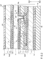
- FIG. 1 is a plan view showing a schematic structure of a display device according to First Embodiment.
- FIG. 2 is a cross-sectional view seen along line F 2 -F 2 of FIG. 1 .
- FIG. 3 is a cross-sectional view seen along line F 3 -F 3 of FIG. 1 .
- FIG. 4 is a plan view schematically showing an example of an alignment pattern of a spacer shown in FIG. 1 .
- FIG. 5 is a plan view schematically showing another example of the alignment pattern shown in FIG. 4 .
- FIG. 6 is a plan view schematically showing yet another example of the alignment pattern shown in FIG. 4 and FIG. 5 .
- FIG. 7 is a plan view schematically showing yet another example of the alignment pattern shown in FIG. 4 , FIG. 5 and FIG. 6 .
- FIG. 8 is a plan view showing a schematic structure of a display device according to Second Embodiment.
- FIG. 9 is a plan view showing a schematic structure of a display device according to Third Embodiment.
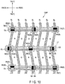
- FIG. 10 is a plan view showing a schematic structure of a display device according to Fourth Embodiment.
- FIG. 11 is a cross-sectional view seen along line F 11 -F 11 of FIG. 10 .
- FIG. 12 is a plan view showing a schematic structure of a display device according to Fifth Embodiment.
- FIG. 13 is a cross-sectional view seen along line F 13 -F 13 of FIG. 12 .
- FIG. 14 is a perspective view showing a schematic structure of a display device according to Sixth Embodiment.
- FIG. 15 is a plan view schematically showing density of first and third sets in an end area and a central area shown in FIG. 14 .
- FIG. 16 is a plan view showing a schematic structure of a display device according to Seventh Embodiment.
- FIG. 17 is a cross-sectional view seen along line F 17 -F 17 of FIG. 16 .
- FIG. 18 is a plan view showing a schematic structure of a display device according to Eighth Embodiment.
- FIG. 19 is a plan view showing a schematic structure of a display device according to Ninth Embodiment.
- a display device comprises a first A spacer, a second A spacer, a third A spacer and a fourth A spacer.
- the first A spacer and the third A spacer are on a first substrate.
- the second A spacer and the fourth A spacer are on a second substrate opposed to the first substrate.
- At least one of the first substrate and the second substrate is a flexible substrate.
- the first A spacer and the second A spacer are aligned in a first direction in planar view.
- the third A spacer and the fourth A spacer are aligned in a second direction intersecting the first direction in planar view.
- Side surfaces of the first A spacer and the second A spacer face in the first direction.
- Side surfaces of the third A spacer and the fourth A spacer face in the second direction.
- a display device DSP which is a liquid crystal display device, will be disclosed as an example of the display device in the following description.
- the display device DSP can be used in various devices such as smartphones, tablet computers, mobile phones, personal computers, television receivers, in-vehicle devices, game consoles and wearable devices.
- FIG. 1 is a plan view showing a schematic structure of the display device DSP according to First Embodiment.
- the display device DSP comprises a plurality of scanning signal lines GL, a plurality of scanning signal lines GL, a plurality of sub-pixels SPX, and a plurality of first to fourth spacers 1 , 2 , 3 , and 4 .
- the scanning signal lines GL extend in the first direction X and are arranged in the second direction Y intersecting the first direction X.
- the video signal lines SL extend in the second direction Y so as to be arranged in the first direction X.
- the video signal lines SL extend in the second direction Y while bent in a zigzag shape.
- the video signal lines SL may be straight lines parallel to the second direction Y or curves meandering in the second direction Y.
- the first direction X and the second direction Y are perpendicular to each other.
- the first direction X includes a first A direction XA and a first B direction XB.
- the first direction X is the lateral direction
- the first A direction XA is the leftward direction
- the first B direction is the rightward direction.
- the second direction Y includes a second A direction YA and a second B direction YB.
- the second direction Y is the longitudinal direction
- the second A direction YA is the upward direction
- the second B direction YB is the downward direction.
- a sub-pixel SPX corresponds to an area sectioned by two adjacent scanning signal lines GL and two adjacent video signal lines SL.
- a pixel PX capable of color display can be constituted by combining three sub-pixels SPX corresponding to red (R), green (G), and blue (B).
- the pixel PX may include the sub-pixel SPX of the other color such as white (W) or include a plurality of sub-pixels SPX of the same color.
- a pixel electrode PE is formed in each of the sub-pixels SPX.
- a common electrode CE extends across the sub-pixel areas SPX.
- Extension directions YP 1 and YP 2 of the pixel electrodes PE are parallel to linear portions of the video signal lines SL curved in the zigzag state and are slightly inclined to the second direction Y.
- extension direction YP 1 When the extension direction YP 1 is inclined to the first A direction XA with respect to the second direction Y, white is visually recognized to be tinged with blue at a deep viewing angle.
- extension direction YP 2 When the extension direction YP 2 is inclined to the first A direction XA with respect to the second direction Y, white is visually recognized to be tinged with yellow at a deep viewing angle.
- the extension directions YP 1 and YP 2 are alternately inclined in the adjacent sub-pixels SPX, the extension directions can mutually compensate for the color difference and improve the viewing angle property.
- an area represented by two-dot-chained lines corresponds to a light-shielding layer 21 which blocks light.
- the light-shielding layer 21 overlaps and covers the scanning signal lines GL, the video signal lines SL, and the first to fourth spacers 1 , 2 , 3 , and 4 .
- the first spacer 1 includes a first A spacer 1 A and a first B spacer 1 B.
- the second spacer 2 includes a second A spacer 2 A and a second B spacer 2 B
- the third spacer 3 includes a third A spacer 3 A and a third B spacer 3 B
- the fourth spacer 4 includes a fourth A spacer 4 A and a fourth B spacer 4 B.
- the first to fourth spacers 1 , 2 , 3 , and 4 will be explained later in detail with reference to FIG. 3 to FIG. 7 .
- FIG. 2 is a cross-sectional view seen along line F 2 -F 2 of FIG. 1 .
- the third direction Z which is the thickness direction of the display device DSP is orthogonal to the first direction X and the second direction Y shown in FIG. 1 .
- the display device DSP is configured to correspond to a display mode mainly using a lateral electric field approximately parallel to the display surface.
- the display device DSP may be configured to correspond to a display mode using a longitudinal electric field perpendicular to the display surface, an electric field inclined to the display surface, or a combination of the electric fields.
- the display device DSP comprises a display panel PNL and an illumination device BL which applies light to the back surface of the display panel PNL.
- the display panel PNL displays an image on the display surface by urging the light incident on the back surface to be transmitted selectively.
- the display panel PNL may be a reflective display panel which displays an image on the display surface by urging the light incident on the display surface to be reflected selectively.
- the display panel PNL comprises a first substrate (array substrate) SUB 1 , a second substrate (counter-substrate) SUB 2 opposed to the first substrate SUB 1 , and a liquid crystal layer LC disposed between the first substrate SUB 1 and the second substrate SUB 2 .
- the first substrate SUB 1 comprises the scanning signal line GL, the video signal line SL, the pixel electrode PE, and the common electrode CE as shown in FIG. 1 .
- the first substrate SUB 1 further comprises a first flexible base 10 , first to fifth insulating layers 11 , 12 , 13 , 14 , and 15 , a semiconductor layer SC, A relay electrode SLr, and a first alignment film AL 1 as shown in FIG. 2 .
- the first flexible base 10 is formed of, for example, polyimide resin and has flexibility, translucency, and insulation property.
- the first substrate SUB 1 comprising the first flexible base 10 as its base is an example of the flexible substrate.
- the first flexible base 10 includes a first surface 10 A opposed to the second substrate SUB 2 and a second surface 10 B on a side opposite to the first surface 10 A.
- a first insulating layer 11 covers the first surface 10 A of the first flexible base 10 .
- the semiconductor layer SC is formed on the first insulating layer 11 .
- the second insulating layer 12 covers the first insulating layer 11 and the semiconductor layer SC.
- the scanning signal lines GL are formed on the second insulating layer 12 .
- the third insulating layer 13 covers the second insulating layer 12 and the scanning signal lines GL.
- the video signal line SL and the relay electrode SLr are formed on the third insulating layer 13 .
- the video signal line SL and the relay electrode SLr can be formed in the same steps.
- the fourth insulating layer 14 covers the third insulating layer 13 , the video signal line SL, and the relay electrode SLr.
- the common electrode CE is formed on the fourth insulating layer 14 .
- a metal layer ML may be formed to overlap the video signal line SL and the scanning signal lines GL.
- the metal layer ML is electrically connected to the common electrode CE.
- the fifth insulating layer 15 covers the fourth insulating layer 14 , the common electrode CE, and the metal layer ML.
- the pixel electrode PE is formed on the fifth insulating layer 15 .
- the pixel electrode PE may be formed under the fifth insulating layer 15
- the common electrode CE may be formed on the fifth insulating layer 15 .
- the fifth insulating layer 15 is an example of an interlayer insulating film which insulates the pixel electrode PE and the common electrode CE from each other.
- the first alignment film AL 1 covers the fifth insulating layer 15 and the pixel electrode PE.
- a first contact hole CH 1 and a second contact hole CH 2 penetrate the second insulating layer 12 and the third insulating layer 13 .
- a third contact hole CH 3 penetrates the fourth insulating layer 14 and the fifth insulating layer 15 .
- the video signal line SL is in contact with the semiconductor layer SC through the first contact hole CH 1 .
- the relay electrode SLr is in contact with the semiconductor layer SC through the second contact hole CH 2 .
- Either of the video signal line SL and the relay electrode SLr is a source electrode and the other is a drain electrode.
- a thin-film transistor (TFT) is composed of the semiconductor layer SC, the source electrode, and the drain electrode.
- the pixel electrode PE is in contact with the relay electrode SLr through the third contact hole CH 3 , and is electrically connected to the semiconductor layer SC.
- a voltage is supplied to the pixel electrode PE via the source electrode, the electric field is generated between the pixel electrodes PE and the common electrode CE to change the alignment of the liquid crystal molecules of the liquid crystal layer LC.
- the amount of light transmitted through the liquid crystal layer LC is thereby controlled.
- the scanning signal lines GL, the video signal line SL, and the metal layer ML are formed of, for example, a metal material having a single-layer structure or a stacked layer structure.
- the video signal line SL may be narrower as compared with the scanning signal line GL.
- the relay electrode SLr is formed of, for example, the same metal material as the video signal line SL.
- the pixel electrode PE and the common electrode CE are transparent conductive films formed of indium tin oxide (ITO), indium zinc oxide (ILO), and the like.
- the semiconductor layer SC is formed of, for example, low temperature polysilicon (LTPS) or high temperature polysilicon (HTPS).
- the first to third and fifth insulating layers 11 , 12 , 13 , and 15 are inorganic insulating layers of silicon oxide, silicon nitride or alumina.
- the fourth insulating layer 14 is, for example, an organic insulating layer formed of photosensitive resin such as acrylic resin.
- the fourth insulating layer 14 has a function of flattening an uneven surface of the thin-film transistor, and is formed to be thicker than the first to third and fifth insulating layers 11 , 12 , 13 , and 15 and the first alignment film AL 1 .
- the fourth insulating layer 14 is an example of a planarizing film.
- the second substrate SUB 2 comprises a second flexible base 20 , a color filter layer 22 , an overcoat layer 23 , and a second alignment film AL 2 in addition to the light-shielding layer 21 shown in FIG. 1 .
- the second flexible base 20 is formed of the same resin material as the first flexible base 10 .
- the second substrate SUB 2 comprising the second flexible base 20 as its base is an example of the flexible substrate.
- the second flexible base 20 includes a third surface 20 A opposed to the first surface 10 A of the first flexible base 10 , and a fourth surface 20 B on the side opposite to the third surface 20 A.
- the light-shielding layer 21 is formed on the third surface 20 A of the second flexible base 20 .
- the color filter layer 22 covers the third surface 20 A and the light-shielding layer 21 .
- the color filter layer 22 is colored to correspond to each sub-pixel SPX.
- the overcoat layer 23 covers the color filter layer 22 .
- the second alignment film AL 2 covers the overcoat layer 23 .
- the liquid crystal layer LC is disposed between the first alignment film AL 1 and the second alignment film AL 2 .
- the first alignment film AL 1 and the second alignment film AL 2 align the liquid crystal molecules of the liquid crystal layer LC in a state in which a voltage is not applied to the pixel electrodes PE.
- the first alignment film AL 1 and the second alignment film AL 2 are, for example, polyimide resin and the like applied by ink jet printing and flexographic printing.
- a first polarizer PL 1 is applied to the second surface 10 B of the first flexible base 10 .
- a second polarizer PL 2 is applied to the fourth surface 20 B of the second flexible base 20 .
- the first polarizer PL 1 may not be disposed.
- the first spacer 1 and the third spacer 3 shown in FIG. 1 i.e., the first A spacer 1 A, the first B spacer 1 B, the third A spacer 3 A, and the third B spacer 3 B are formed on the first substrate SUB 1 .
- the second spacer 2 and the fourth spacer 4 shown in FIG. 1 i.e., the second A spacer 2 A, the second B spacer 2 B, the fourth A spacer 4 A, and the fourth B spacer 4 B are formed on the second substrate SUB 2 .
- the first B spacer 1 B, the third A spacer 3 A, and the third B spacer 3 B have substantially the same shape and function as the first A spacer 1 A.
- the first A spacer 1 A will be explained in detail as a representative spacer, and duplicate explanations of the first B spacer 1 B, the third A spacer 3 A, and the third B spacer 3 B will be omitted.
- the second B spacer 2 B, the fourth A spacer 4 A, and the fourth B spacer 4 B have substantially the same shape and function as the second A spacer 2 A.
- the second A spacer 2 A will be explained in detail as a representative spacer, and duplicate explanations of the second B spacer 2 B, the fourth A spacer 4 A, and the fourth B spacer 4 B will be omitted.
- FIG. 3 is a cross-sectional view seen along line F 3 -F 3 of FIG. 1 .
- the first A spacer 1 A is formed on the fifth insulating layer 15 and covered with the first alignment film AL 1 .
- the second A spacer 2 A is formed on the overcoat layer 23 and covered with the second alignment film AL 2 .
- the first A spacer 1 A and the second A spacer 2 A are formed of, for example, photosensitive acrylic resin or the like.
- the display device DSP has a characteristic that the first A spacer 1 A and the second A spacer 2 A do not overlap in planar view.
- a height Z 1 of the first A spacer 1 A which is disposed not to overlap the second A spacer 2 A is not limited by a height Z 2 of the second A spacer 2 A.
- the height Z 1 of the first A spacer 1 A and the height Z 2 of the second A spacer 2 A can be freely selected within a cell gap Z 0 that is the interval between the first substrate SUB 1 and the second substrate SUB 2 .
- the height Z 1 of the first A spacer 1 A is formed to be lower than the cell gap Z 0 and higher than a half of the cell gap Z 0 .
- the height Z 2 of the second A spacer 2 A is formed to be substantially the same as the cell gap Z 0 .
- the first A spacer 1 A is not in contact with the second substrate SUB 2 while the second A spacer 2 A is in contact with the first substrate SUB 1 via the first alignment film AL 1 and the second alignment film AL 2 .
- the height Z 1 of the first A spacer 1 A may be formed to be substantially the same as the cell gap Z 0 and the height Z 2 of the second A spacer 2 A may be formed to be lower than the cell gap Z 0 .
- a contact area of the side surfaces of the upper and lower spacers can be increased as compared with a configuration that the recess portion is formed at the distal end of the spacer of the second substrate SUB 2 , the spacer (base) is formed on the first substrate SUB 1 to overlap the recess portion, and the side surface of the spacer of the second substrate SUB 2 is made to abut on the side surface of the spacer of the first substrate SUB 1 to prevent movement of the second substrate SUB 2 .
- a contact surface Z 12 on which the side surface 1 As of the first A spacer 1 A is in contact with the side surface 2 As of the second A spacer 2 A is wider than a half of the cell gap Z 0 .
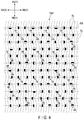
- FIG. 4 is a plan view schematically showing the first A to fourth B spacers 1 A, 1 B, 2 A, 2 B, 3 A, 3 B, 4 A, and 4 B shown in FIG. 1 .
- the first A spacers 1 A and the first B spacers 1 B are aligned in the first direction X
- the third A spacers 3 A and the third B spacers 3 B are aligned in the second direction Y.
- the first A spacers 1 A, the first B spacers 1 B, the third A spacers 3 A, and the third B spacer 3 B are formed in intersection areas GS where the scanning signal lines GL and the video signal lines SL intersect.
- the spacers may be formed at positions remote from the intersection areas GS.
- Each of the second A spacers 2 A is disposed to be adjacent to the first A spacer 1 A, and each of the second B spacers 2 B is disposed to be adjacent to the first B spacer 1 B.
- Each of the fourth A spacers 4 A is disposed to be adjacent to the fourth A spacer 4 A, and each of the fourth B spacers 4 B is disposed to be adjacent to the fourth B spacer 4 B.
- the first A spacer 1 A is located in a first A direction (leftward direction) XA with respect to the adjacent second A spacer 2 A.
- the first B spacer 1 B is located in a first B direction (rightward direction) XB with respect to the adjacent second B spacer 2 B
- the third A spacer 3 A is located in a second A direction (upward direction) with respect to the adjacent fourth A spacer 4 A
- the third B spacer 3 B is located in a second B direction (downward direction) with respect to the adjacent fourth B spacer 4 B.
- a pair of the first A spacer 1 A and the second A spacer 2 A adjacent to each other is called a first set S 1
- a pair of the third A spacer 3 A and the fourth A spacer 4 A adjacent to each other is called a first set S 2
- a pair of the first B spacer and the second B spacer adjacent to each other is called a third set S 3
- a pair of the third B spacer 3 B and the fourth B spacer 4 B adjacent to each other is called a fourth set S 4 .
- the first to fourth sets S 1 , S 2 , S 3 , and S 4 are examples of stoppers which suppress the displacement of the second substrate SUB 2 from the first substrate SUB 1 .
- the side surfaces 1 As and 2 As of the first A spacer 1 A and second A spacer 2 A constituting the first set S 1 are opposed to each other in the first direction X.
- the side surfaces of the third A spacer 3 A and third A spacer 4 A constituting the second set S 2 are opposed to each other in the second direction Y.
- the side surfaces of the first B spacer 1 B and second B spacer 2 B constituting the third set S 3 are opposed to each other in the first direction X.
- the side surfaces of the third B spacer 3 B and third B spacer 4 B constituting the fourth set S 4 are opposed to each other in the second direction Y.
- FIG. 5 to FIG. 7 are plan views schematically showing another example of the alignment pattern of the spacers shown in FIG. 4 .
- the first to fourth sets S 1 , S 2 , S 3 , and S 4 are aligned in the intersection areas GS where third, sixth, ninth, . . . 3 N video signal lines SL from the left and the scanning signal lines GL intersect.
- the alignment pattern is not limited to this.
- the first to fourth sets S 1 , S 2 , S 3 , and S 4 may be aligned while shifting the video signal line SL to the right adjacent or left adjacent video signal line SL in the second direction YB.
- the first to fourth sets S 1 , S 2 , S 3 , and S 4 may be aligned while alternately shifting the video signal lines SL to the even-numbered and odd-numbered video signal lines SL.
- the first to fourth sets S 1 , S 2 , S 3 , and S 4 may be aligned for every two or less video signal lines SL or the first to fourth sets S 1 , S 2 , S 3 , and S 4 may be aligned for every four or more video signal lines SL. Density of the first to fourth sets S 1 , S 2 , S 3 , and S 4 can be adjusted in accordance with the usage and site of the display device DSP, by combining various alignment patterns.
- the first to fourth sets S 1 , S 2 , S 3 , and S 4 are aligned such that the density of the first set S 1 and the third set S 3 suppressing the displacement in the first direction X is higher than the density of the second set S 2 and the fourth set S 4 suppressing the displacement in the second direction Y.
- the spacers are formed in the first substrate SUB 1 and the second substrate SUB 2 , respectively.
- the spacers ( 1 A, 1 B, 3 A, and 3 B) formed in the first substrate SUB 1 and the spacers ( 2 A, 2 B, 4 A, and 4 B) formed in the second substrate SUB 2 are arranged adjacently not to overlap in planar view, and constitute the stoppers which suppress the displacement of the second substrate SUB 2 from the first substrate SUB 1 , i.e., the first to fourth sets S 1 , S 2 , S 3 , and S 4 .
- the side surface 1 As of the first A spacer 1 A constituting the first set S 1 abuts on the side surface 2 As of the second A spacer 2 A to prevent the movement of the second substrate SUB 2 , as shown in FIG. 1 .
- the side surface of the first B spacer 1 B constituting the third set S 3 abuts on the side surface of the second B spacer 2 B to prevent the movement of the second substrate SUB 2 .
- the side surface of the third A spacer 3 A constituting the second set S 2 abuts on the side surface of the fourth A spacer 4 A to prevent the movement of the second substrate SUB 2 .
- the side surface of the second B spacer 3 B constituting the fourth set S 4 abuts on the side surface of the fourth B spacer 4 B to prevent the movement of the second substrate SUB 2 .
- the movement of the second substrate SUB 2 can be prevented by the spacers constituting the first to fourth sets S 1 , S 2 , S 3 , and S 4 .
- the displacement of the second substrate SUB 2 from the first substrate SUB 1 can be suppressed more effectively and occurrence of color mixture can be suppressed.
- a pair of spacers constituting the stopper are disposed not to overlap in planar view.
- a height of one of the spacers is not limited by a height of the other spacer. Since the height of each of the spacers of the first substrate SUB 1 and the second substrate SUB 2 can be set freely, the spacer can be formed to have a height enough to suppress the displacement.
- the light-shielding layer 21 is formed to be large in accordance with the displacement, the light applied from the illumination device BL is blocked by the light-shielding layer 21 and the display surface becomes dark. Since the First Embodiment can effectively suppress the displacement, the size of the light-shielding layer 21 can be made smaller. The light applied from the illumination device BL can be used effectively and the power consumption can be saved.
- the displacement in the first direction X gives a greater influence to occurrence of the color mixture and the like than the displacement in the second direction Y.
- the first to fourth sets S 1 , S 2 , S 3 , and S 4 are aligned such that the density of the first set S 1 and the third set S 3 suppressing the displacement in the first direction X is higher than the density of the second set S 2 and the fourth set S 4 suppressing the displacement in the second direction Y. According to this alignment pattern, the displacement in the first direction X can be suppressed effectively.
- various preferable advantages can be obtained from the First Embodiment.
- FIG. 8 is a plan view showing a schematic structure of a display device DSP according to Second Embodiment.
- the Second Embodiment is different from the First Embodiment with respect to a feature that first C and fourth D spacers 1 C, 1 D, 2 C, 2 D, 3 C, 3 D, 4 C, and 4 D are formed instead of the first A to fourth B spacers 1 A, 1 B, 2 A, 2 B, 3 A, 3 B, 4 A, and 4 B.
- Second C and fourth D spacers 3 C, 3 D, 4 C, and 4 D exist on the same plane in the first direction X and the second direction Y and extend in a fourth direction V intersecting the first direction X and the second direction Y.
- Side surfaces of first C and second D spacers 1 C, 1 D, 2 C, and 2 D exist on the same plane in the first direction X, the second direction Y, and the fourth direction V and the and extend in a fifth direction W intersecting the first direction X, the second direction Y, and the fourth direction V.
- the fourth direction V and the fifth direction W are orthogonal to the third direction (thickness direction) Z shown in FIG. 3 .
- the fourth direction V is inclined counterclockwise at 45 degrees with respect to the first direction X
- the fifth direction W is inclined counterclockwise at 45 degrees with respect to the second direction Y.
- the inclination of the fourth direction V for the first direction X and the inclination of the fifth direction W for the second direction Y are arbitrarily set and are not limited to these.
- the fourth direction V includes a fourth A direction VA and a fourth B direction VB.
- the fourth A direction YA is a leftward and downward direction
- the fourth B direction is a rightward and upward direction
- the fifth direction W includes a fifth A direction WA and a fifth B direction WB.
- the fifth A direction WA is a leftward and upward direction
- the fifth B direction WB is a rightward and downward direction.
- the first C spacer 1 C extending in the fifth direction W is located in the fourth A direction (leftward and downward direction) VA with respect to the adjacent second C spacer 2 C.
- side surfaces 1 Cs and 1 Cs of the first C and second C spacers 1 C overlap in the first direction X and also overlap in the second direction Y.
- the second D spacer 1 D is located in a fourth B direction (rightward and upward direction) VB with respect to the adjacent second D spacer 2 D
- the third C spacer 2 A is located in a fifth A direction (leftward and upward direction) with respect to the adjacent fourth C spacer 4 A
- the third D spacer 3 D is located in a fifth B direction (rightward and downward direction) with respect to the adjacent fourth D spacer 4 D.
- the side surfaces of the adjacent spacers overlap in the first direction X and also overlap in the second direction Y.
- a pair of the first C spacer 1 C and the second C spacer 2 C adjacent to each other is called a fifth set S 5
- a pair of the third C spacer 3 C and the fourth C spacer 4 C adjacent to each other is called a sixth set S 6
- a pair of the first D spacer and the second D spacer adjacent to each other is called a seventh set S 7
- a pair of the third D spacer 3 D and the fourth D spacer 4 D adjacent to each other is called an eighth set S 8 .
- the fifth to eighth sets S 5 , S 6 , S 7 , and S 8 are formed in an approximately rectangular shape in planar view and include first to fourth corners (four corners) C 1 , C 2 , C 3 , and C 4 , respectively.
- the first corner C 1 and the third corner C 3 that are a pair of opposite angles are disposed side by side in the first direction X, and overlap the light-shielding layer 21 extending along the scanning signal lines GL, in planar view.
- the second corner C 2 and the fourth corner C 4 that are another pair of opposite angles are disposed side by side in the second direction Y, and overlap the light-shielding layer 21 extending along the scanning signal lines GL, in planar view.
- the second corner C 2 and the fourth corner C 4 overlap the video signal line SL in planar view.
- a pair of opposite angles are disposed side by side in the first direction X, and overlap the light-shielding layer 21 extending along the scanning signal lines GL, in planar view.
- Another pair of opposite angles are disposed side by side in the second direction Y, and overlap the light-shielding layer 21 extending along the scanning signal lines GL, in planar view.
- the second substrate SUB 2 When the second substrate SUB 2 is moved from the first substrate SUB 1 in the opposite direction, i.e., the first B direction XB, the side surface of the first D spacer 1 D abuts on the side surface of the second D spacer 2 D, the side surface of the third D spacer 3 D abuts on the side surface of the fourth D spacer 4 D, and the movement of the second substrate SUB 2 is thereby prevented.
- the second substrate SUB 2 When the second substrate SUB 2 is moved from the first substrate SUB 1 in the opposite direction, i.e., the second B direction YB, the side surface of the first C spacer 1 C abuts on the side surface of the second C spacer 2 C, the side surface of the third D spacer 3 D abuts on the side surface of the fourth D spacer 4 D, and the movement of the second substrate SUB 2 is thereby prevented.
- the movement of the second substrate SUB 2 can be prevented by the spacers constituting the first C to fourth D spacers 1 C, 1 D, 2 C, 2 D, 3 C, and 3 D, and the displacement of the second substrate SUB 2 from the first substrate SUB 1 can be suppressed effectively.
- four corners C 1 , C 2 , C 3 , and C 4 of the fifth to eighth sets S 5 , S 6 , S 7 , and S 8 are disposed to overlap the light-shielding layer 21 extending along the video signal line SL or the scanning signal lines GL, in planar view. Since the light-shielding layer 21 extending along the video signal line SL and the scanning signal lines GL can be used at most parts of the light-shielding layer 21 formed to cover the spacers, the size of the light-shielding layer 21 serving as the entire body of the display device DSP can be made smaller. The light applied from the illumination device BL can be used effectively and the power consumption can be saved.
- FIG. 9 is a plan view showing a schematic structure of a display device DSP according to Third Embodiment.
- the Third Embodiment is different from the First Embodiment with respect to features that pixels PX further include white (W) sub-pixels SPX, and that first to fourth sets S 1 , S 2 , S 3 , and S 4 are disposed to avoid red (R), green (G), and blue (B) sub-pixels SPX and to overlap end portions of the white (W) sub-pixels SPX.
- a pixel PX includes two red (R) sub-pixels SPX, two green (G) sub-pixels SPX, one blue (B) sub-pixel SPX, and one white (W) sub-pixel SPX.
- R red
- G green
- B blue
- W white
- the pixel PX may include one red (R) sub-pixels SPX, one green (G) sub-pixel SPX, one blue (B) sub-pixel SPX, and one white (W) sub-pixel SPX, or may include two or more blue (B) sub-pixels SPX, or may three or more red (R) and green (G) sub-pixels SPX.
- the blue (B) sub-pixel SPX has lower visibility than the green (G) and red (R) sub-pixels SPX.
- the number of the green (G) and red (R) sub-pixels SPX is desirably more than or equal to the number of the blue (B) sub-pixels SPX.
- the movement of the second substrate SUB 2 can be prevented by the spacers constituting the first to fourth sets S 1 , S 2 , S 3 , and S 4 and the displacement of the second substrate SUB 2 from the first substrate SUB 1 can be suppressed effectively.
- the Third Embodiment includes the white (W) sub-pixel SPX, a white component generated by the red (R), green (G), and blue (B) sub-pixels SPX can be replaced with the white (W) sub-pixel SPX.
- the white (W) sub-pixel SPX has a higher light transmittance than the red (R), green (G), and blue (B) sub-pixels SPX, the light applied from the illumination device BL to the display panel PNL can be used efficiently.
- the power consumption of the illumination device BL can be reduced with the same screen luminance, and the screen luminance can be increased and the visibility can be improved with the same power consumption.
- the light-shielding layer 21 covering the first to fourth sets S 1 , S 2 , S 3 , and S 4 is formed so as to overlap not the red (R), green (G), and blue (B) sub-pixels SPX, but the white (W) sub-pixel SPX in planar view.
- the red (R), green (G), and blue (B) sub-pixels SPX are not hidden by the light-shielding layer 21 or do not become so much small. Displacement between the substrates can be suppressed while maintaining the balance in color matching and the screen luminance.
- FIG. 10 is a plan view showing a schematic structure of the display device DSP according to Fourth Embodiment.
- the Fourth Embodiment is different from the First Embodiment with respect to features that several or all parts of a first spacer 1 and a second spacer 2 are replaced with a fifth spacer 5 and a sixth spacer 6 and that several or all parts of a third spacer 3 and a fourth spacer 4 are replaced with a seventh spacer 7 and an eighth spacer 8 .
- the fifth spacer 5 and the seventh spacer 7 are formed on a first substrate SUB 1 .
- the sixth spacer 6 and the eighth spacer 8 are formed on a second substrate SUB 2 .
- One of features of the embodiment is that the fifth spacer 5 and the sixth spacer 6 do not overlap in planar view similarly to the first spacer 1 and the second spacer 2 .
- One of features of the embodiment is that the seventh spacer 7 and the eighth spacer 8 do not overlap in planar view similarly to the third spacer 3 and the fourth spacer 4 .
- the fifth spacer 5 includes a fifth A spacer 5 A and a fifth B spacer 5 B
- the sixth spacer 6 includes a sixth A spacer 6 A and a sixth B spacer 6 B
- the seventh spacer 7 includes a seventh A spacer 7 A and a seventh B spacer 7 B
- the eighth spacer 8 includes an eighth A spacer 8 A and an eighth B spacer 8 B.
- FIG. 11 is a cross-sectional view seen along line F 8 -F 8 of FIG. 10 .
- the fifth A spacer 5 A has substantially the same shape and function as the first A spacer 1 A shown in FIG. 3 and is aligned similarly to the first A spacer 1 A.
- the sixth A spacer 6 A has substantially the same shape and function as the second A spacer 2 A shown in FIG. 3 except a height Z 6 , and is aligned similarly to the second A spacer 2 A.
- the fifth B spacer 5 B, the seventh A spacer 7 A, and the seventh B spacer 7 B shown in FIG. 10 have substantially the same shape and function as the fifth A spacer 5 A shown in FIG. 11
- the sixth B spacer 6 B, the eighth A spacer 8 A, and the eighth B spacer 8 B have substantially the same shape and function as the sixth A spacer 6 A.
- the fifth B spacer 5 B is aligned similarly to the first B spacer 1 B shown in FIG.
- the sixth B spacer 6 B is aligned similarly to the second B spacer 2 B
- the seventh A spacer 7 A is aligned similarly to the third A spacer 3 A
- the seventh B spacer 7 B is aligned similarly to the third B spacer 3 B
- the eighth A spacer BA is aligned similarly to the eighth A spacer 8 A
- the eighth B spacer 8 B is aligned similarly to the eighth B spacer 8 B.
- the fifth A spacer 5 A and the sixth A spacer 6 will be explained in detail as a representative spacers, and duplicate explanations of the fifth B spacer 5 B, the sixth B spacer 6 B, the seventh A spacer 7 A, the seventh A spacer 7 A, the seventh B spacer 7 B, the eighth A spacer 8 A, and the eighth B spacer 8 B will be omitted.
- the fifth A spacer 5 A is not in contact with the second substrate SUB 2
- the sixth A spacer 6 A is not in contact with the first substrate SUB 1 .
- At least one of the fifth A spacer 5 A and the sixth A spacer 6 A is formed to be higher than a half of a cell gap Z 0 of the first substrate SUB 1 and the second substrate SUB 2 , and a side surface 5 As of the fifth A spacer 5 A and a side surface 6 As of the sixth A spacer 6 A are opposed to each other in the first direction X.
- the side surface 5 As of the fifth A spacer 5 A abuts on the side surface 6 As of the sixth A spacer 6 A to prevent movement of the second substrate SUB 2 .
- the second substrate SUB 2 is flatter than the first substrate SUB 1 on which the thin-film transistor is formed, the height of the spacers can easily be adjusted.
- the fifth A spacer 5 A is formed to be higher than a half of the cell gap Z 0
- the sixth A spacer 6 A formed on the second substrate SUB 2 is formed to be further higher than the fifth A spacer 5 A formed on the first substrate SUB 1 .
- a height Z 5 of the fifth A spacer 5 A which is disposed not to overlap the sixth A spacer 6 A is not limited by a height Z 6 of the sixth A spacer 6 A.
- a contact area of the side surfaces of the upper and lower spacers can be increased as compared with the structure that the recess portion is formed on the tip of the second substrate SUB 2 and the spacer (pedestal portion) is formed on the first substrate SUB 1 to overlap the recess portion.
- a contact surface Z 56 on which the side surface 5 As of the fifth A spacer 5 A is in contact with the side surface 6 As of the sixth A spacer 6 A is wider than a quarter of the cell gap Z 0 .
- the Fourth Embodiment can suppress the displacement between the substrates by the fifth spacer 5 , the sixth spacer 6 , the seventh spacer 7 , and the eighth spacer 8 . If an external force is excessively applied after suppression of the displacement, the spacer formed on the second substrate SUB 2 may ride on the spacer formed on the first substrate SUB 1 . If the second spacer 2 having substantially the same height Z 2 as the cell gap Z 0 rides on the first spacer 1 , the cell gap Z 0 may be varied greatly and locally and the display quality may be degraded.
- the second spacer 2 and the fourth spacer 4 are replaced with the sixth spacer 6 and the eighth spacer 8 lower than the second spacer 2 and the fourth spacer 4 .
- the spacer formed on the second substrate SUB 2 rides on the spacer formed on the first substrate SUB 1 , degradation of the display quality can be made inconspicuous by making the variation in the cell gap Z 0 smaller.
- FIG. 12 is a plan view showing a schematic structure of the display device DSP according to Fifth Embodiment.
- the Fifth Embodiment is different from the First Embodiment with respect to features that several parts of a third spacer 3 and a fourth spacer 4 are replaced with a ninth spacer 9 , that remainders of the third spacer 3 and the fourth spacer 4 are replaced with a seventh spacer 7 and an eighth spacer 8 , and that all parts of a first spacer 1 and a second spacer 2 are replaced with a fifth spacer 5 and a sixth spacer 6 .
- none of the first to fourth spacers 1 , 2 , 3 , and 4 is formed in the Fifth Embodiment.
- FIG. 13 is a cross-sectional view seen along line F 13 -F 13 of FIG. 12 .
- a height Z 9 of the ninth spacer 9 is formed to be substantially the same as a cell gap Z 0 .
- the ninth spacer 9 is formed on the second substrate SUB 2 and is in contact with the first substrate SUB 1 via a first alignment film AL 1 and a second alignment film AL 2 .
- a surface of the first substrate SUB 1 opposed to the ninth spacer 9 rises as compared with the other surface by a video signal line SL, other metal lines, or a fifth insulating layer 15 .
- the ninth spacer 9 may be formed on the first substrate SUB 1 or may be formed on each of the first substrate SUB 1 and the second substrate SUB 2 to overlap the substrates in planar view.
- the height Z 9 of the sum of the height of the ninth spacer 9 formed on the first substrate SUB 1 and the height of the other ninth spacer 9 formed on the second substrate SUB 2 may be substantially the same as the cell gap Z 0 .
- the ninth spacer 9 is an example of a conventional spacer which constantly maintains the cell gap Z 0 .
- the displacement of the second substrate SUB 2 from the first substrate SUB 1 can be suppressed by the fifth spacer 5 and the sixth spacer 6 , similarly to the Fourth Embodiment.
- the fourth spacer 4 since none of the first to fourth spacers 1 , 2 , 3 , and 4 is disposed, there is no risk that the second spacer 2 may ride on the first spacer 1 , the fourth spacer 4 may ride on the third spacer 3 , and the cell gap Z 0 may be thereby varied.
- the cell gap Z 0 is maintained constant by not the second spacer 2 or the fourth spacer 4 , but the ninth spacer 9 .
- FIG. 14 is a plan view showing a schematic structure of the display device DSP according to Sixth Embodiment.
- the Sixth Embodiment is different from the First Embodiment with respect to a feature that spacers are aligned while varying a density of each of a first set S 1 and a third set S 3 , in an end area (left edge area) A 1 of a first A direction XA, an end area (right edge area) A 2 of a first B direction XB, and a central area A 3 between the end areas A 1 and A 2 .
- FIG. 15 is a plan view schematically showing density of the first set S 1 and the third set S 3 in the end areas A 1 and A 2 and the central area A 3 .
- the first set S 1 and the third set S 3 are aligned such that the density of the third set S 3 suppressing the movement of the second substrate SUB 2 to the first B direction XB is higher than the density of the first set S 1 suppressing the movement in the opposite direction, in the end area A 1 which allows the second substrate SUB 2 to move in the first B direction XB.
- first to fourth sets S 1 , S 2 , S 3 , and S 4 are aligned such that the density of the first set S 1 suppressing the movement of the second substrate SUB 2 to the first A direction XA is higher than the density of the third set S 3 suppressing the movement in the opposite direction, in the end area A 2 which allows the second substrate SUB 2 to move in the first A direction XA.
- the first to fourth sets S 1 , S 2 , S 3 , and S 4 are aligned such that the density of the first set S 1 is substantially the same as the density of the third set S 3 .
- the density of the first set S 1 is higher in the end area A 3 in the first B direction than in the central area A 3
- the density of the third set S 3 is higher in the end area A 1 in the first A direction than in the central area A 3 .
- the Sixth Embodiment can endure a larger stress as compared with a case where the first set S 1 and the third set S 3 are disposed half-and-half. Even if the bending of the end areas A 1 and A 3 becomes large, the displacement of the second substrate SUB 2 can be suppressed effectively.
- FIG. 16 is a plan view showing a schematic structure of the display device DSP according to Seventh Embodiment.
- Seventh Embodiment is, for example, a high-definition display device employed for a head-mounted display or the like.
- the first to fourth spacers 1 , 2 , 3 , and 4 and the fifth to eighth spacers 5 , 6 , 7 , and 8 are disposed together.
- the video signal lines SL are not bent but extend linearly in parallel with the second direction Y. If the video signal lines SL extend linearly, a light-shielding layer 21 covering the video signal lines SL can be formed to have a small width. Extension directions YP 1 and YP 2 of pixel electrodes PE may be slightly inclined with respect to the second direction Y or may be parallel to the second direction Y.
- a common electrode CE includes a slit OP in a sub-pixel SPX.
- the pixel electrode PE extends in the slit OP.
- Scanning signal lines GL are formed to be wider than the video signal lines S. For this reason, the light-shielding layer 21 extending along the scanning signal lines GL is wider than the light-shielding layer 21 extending along the video signal lines SL.
- the sub-pixels SPX become smaller in accordance with higher definition. Spacers need to be formed in accordance with the sub-pixels SPX but the exposure accuracy is limited. In a case where, for example, the number of pixels is 1000 ppi or more, when the spacers cannot be further narrowed in the width direction, the only length in the extension direction can be adjusted.
- a third spacer 3 , a fourth spacer 4 , a seventh spacer 7 , and an eighth spacer 8 extending in the first direction X are disposed to overlap the light-shielding layer 21 extending along the scanning signal lines GL.
- a fifth spacer 5 and a sixth spacer 6 extending in the second direction Y largely expand over the light-shielding layer 21 extending along the video signal lines SL, the spacers are moved approximately to centers of the sub-pixels SPX in the first direction X and overlap end portions of the sub-pixels SPX.
- the third spacer 3 , the fourth spacer 4 , the seventh spacer 7 , and the eighth spacer 8 extending along the scanning signal lines GL can use the light-shielding layer 21 extending along the scanning signal lines GL at most parts of the light-shielding layer 21 formed to cover the longer spacers.
- the area of the sub-pixels SPX hidden by the light-shielding layer 21 covering the spacers is small.
- the fifth spacer 5 and the sixth spacer 6 disposed to overlap the end portions of the sub-pixels SPX in planar view become longer in the extension direction, the area of the end portions of the sub-pixels SPX hidden by the light-shielding layer 21 covering the fifth spacer 5 and the sixth spacer 6 is large. Since lengths Y and Y 6 of the fifth spacer 5 and the sixth spacer 6 are greatly influenced by the shape of the sub-pixels SPX, the lengths Y 5 and Y 6 of the fifth spacer 5 and the sixth spacer 6 extending in the second direction Y are formed to be shorter than lengths X 7 and X 8 of the seventh spacer 7 and the eighth spacer 8 extending in the first direction X, in the example illustrated in FIG. 17 .
- FIG. 17 is a cross-sectional view seen along line F 13 -F 13 of FIG. 16 .
- the pixel electrode PE is formed under a fifth insulating layer 15
- the common electrode CE is formed on the fifth insulating layer 15 .
- a material to form the spacers is, for example, photosensitive acrylic resin or the like, and has a small adherence to the fifth insulating layer 15 which is an interlayer insulating film.
- the spacers are formed to contact the common electrode CE which is a transparent conductive film having a better adherence to the material of the spacers than the fifth insulating layer 15 .
- the displacement of the second substrate SUB 2 from the first substrate SUB 1 can be suppressed by various spacers, similarly to the First Embodiment.
- the spacers also become smaller in accordance with higher definition. If the spacer size becomes smaller and the area of contact with the base becomes smaller, the spacers may be peeled off when an external force is applied excessively. In the Seventh Embodiment, even if the spacers become smaller, the spacers are formed on the transparent conductive film having a good adherence and the spacers can be firmly adhered to the transparent conductive film.
- the lengths X 7 and X 8 of the seventh spacer 7 and the eighth spacer 8 extending in the first direction X are formed to be shorter than the lengths Y 5 and Y 6 of the fifth spacer 5 and the sixth spacer 6 extending in the second direction Y, in the Seventh Embodiment.
- the area of the sub-pixels SPX hidden by the light-shielding layer 21 of the spacers can be minimized and the displacement can be suppressed without sacrificing the screen luminance.
- FIG. 18 is a plan view showing a schematic structure of the display device DSP according to Eighth Embodiment.
- the Eighth Embodiment similarly to the Fifth Embodiment, none of first to fourth spacers 1 , 2 , 3 , and 4 is formed.
- the other constituent elements are the same as those of the Seventh Embodiment.
- the displacement of a second substrate SUB 2 from a first substrate SUB 1 can be suppressed by fifth to sixth spacers 4 , 5 , 6 , and 7 , similarly to the Seventh Embodiment.
- the spacer formed on the second substrate SUB 2 may ride on the spacer formed on the first substrate SUB 1 . If the second spacer 2 having substantially the same height Z 2 as the cell gap Z 0 rides on the first spacer 1 , the cell gap Z 0 may be varied greatly and locally and the display quality may be degraded.
- the planarizing film such as a fourth insulating layer 14 becomes thinner. If the planarizing film is thinner, protrusion of the video signal lines SL cannot be completely planarized. In a configuration that ninth spacers 9 abut on the video signal lines SL and maintain the cell gap Z 0 , if the ninth spacers 9 slide down from the protruding video signal lines SL, the cell gap Z 0 may be varied.
- the ninth spacers 9 extend in the first direction X intersecting the video signal lines SL. If the ninth spacers 9 are long in the first direction X, a risk that the ninth spacer 9 may slide down from the video signal lines SL can be made smaller even if the second substrate SUB 2 is slightly displaced in the first direction X.
- FIG. 19 is a plan view showing a schematic structure of the display device DSP according to Ninth Embodiment.
- the display device DSP of the Fourth Embodiment is different from the First Embodiment with respect to a feature that projections and depressions are formed on a planarizing film such as a fourth insulating layer 14 and are constituted as spacers (a first spacer 1 , a third spacer 3 , a fifth spacer 5 , a seventh spacer 7 , and the like) of a first substrate SUB 1 .
- the thickness of the fourth insulating layer 14 may be adjusted for each site by multi-tone processing such as halftone processing.
- the thickness of the fourth insulating layer 14 at a site 14 H which is not subjected to the multi-tone processing is, for example, 3 ⁇ m.
- the thickness of the fourth insulating layer 14 at a site 14 L which is subjected to the halftone processing is, for example, 1.5 ⁇ m.
- the displacement of the second substrate SUB 2 from the first substrate SUB 1 can be suppressed by various spacers, similarly to the First Embodiment.
- a step of depositing the spacers on the first substrate SUB 1 can be omitted.
- FIG. 1 and FIG. 16 show an example of a double-gate type switching element in which the semiconductor layer SC intersects the scanning signal lines GL at two times, but the switching element may be a single-gate type switching element.
- FIG. 2 and FIG. 17 show an example that the common electrode CE is provided on the first substrate SUB 1 , but the common electrode CE may be provided on the second substrate SUB 2 .
- the end areas in the first A and first B directions may be curved.
- the first to fourth sets S 1 , S 2 , S 3 , and S 4 may be aligned such that the density of the fourth set S 4 is higher than the density of the second set S 2 in the end area in the second A direction
- the first to fourth sets S 1 , S 2 , S 3 , and S 4 may be aligned such that the density of the second set S 2 is higher than the density of the fourth set S 4 in the end area in the second B direction.
Landscapes
- Physics & Mathematics (AREA)
- Nonlinear Science (AREA)
- Mathematical Physics (AREA)
- Chemical & Material Sciences (AREA)
- Crystallography & Structural Chemistry (AREA)
- General Physics & Mathematics (AREA)
- Optics & Photonics (AREA)
- Engineering & Computer Science (AREA)
- Microelectronics & Electronic Packaging (AREA)
- Devices For Indicating Variable Information By Combining Individual Elements (AREA)
- Liquid Crystal (AREA)
Abstract
Description
Claims (16)
Priority Applications (1)
| Application Number | Priority Date | Filing Date | Title |
|---|---|---|---|
| US17/038,413 US11460733B2 (en) | 2017-05-30 | 2020-09-30 | Display device |
Applications Claiming Priority (2)
| Application Number | Priority Date | Filing Date | Title |
|---|---|---|---|
| JP2017107018A JP2018205358A (en) | 2017-05-30 | 2017-05-30 | Display device |
| JP2017-107018 | 2017-05-30 |
Related Child Applications (1)
| Application Number | Title | Priority Date | Filing Date |
|---|---|---|---|
| US17/038,413 Continuation US11460733B2 (en) | 2017-05-30 | 2020-09-30 | Display device |
Publications (2)
| Publication Number | Publication Date |
|---|---|
| US20180348555A1 US20180348555A1 (en) | 2018-12-06 |
| US10831069B2 true US10831069B2 (en) | 2020-11-10 |
Family
ID=64460531
Family Applications (2)
| Application Number | Title | Priority Date | Filing Date |
|---|---|---|---|
| US15/947,324 Active 2038-10-09 US10831069B2 (en) | 2017-05-30 | 2018-04-06 | Display device |
| US17/038,413 Active 2038-11-09 US11460733B2 (en) | 2017-05-30 | 2020-09-30 | Display device |
Family Applications After (1)
| Application Number | Title | Priority Date | Filing Date |
|---|---|---|---|
| US17/038,413 Active 2038-11-09 US11460733B2 (en) | 2017-05-30 | 2020-09-30 | Display device |
Country Status (2)
| Country | Link |
|---|---|
| US (2) | US10831069B2 (en) |
| JP (1) | JP2018205358A (en) |
Cited By (2)
| Publication number | Priority date | Publication date | Assignee | Title |
|---|---|---|---|---|
| US11489032B2 (en) * | 2019-04-03 | 2022-11-01 | Boe Technology Group Co., Ltd. | Display panel and display device with light shielding portions having curved profile |
| US12501787B2 (en) | 2019-04-03 | 2025-12-16 | Boe Technology Group Co., Ltd. | Display panel and display device with curved light-shielding portions |
Families Citing this family (8)
| Publication number | Priority date | Publication date | Assignee | Title |
|---|---|---|---|---|
| JP2018165779A (en) * | 2017-03-28 | 2018-10-25 | 株式会社ジャパンディスプレイ | Display device |
| JP2019028139A (en) * | 2017-07-26 | 2019-02-21 | 株式会社ジャパンディスプレイ | Display device |
| CN111522178B (en) * | 2019-02-01 | 2023-06-20 | 群创光电股份有限公司 | Liquid crystal display device having a light shielding layer |
| JP2020140170A (en) * | 2019-03-01 | 2020-09-03 | 株式会社ジャパンディスプレイ | Display |
| JP7408456B2 (en) * | 2020-03-26 | 2024-01-05 | 株式会社ジャパンディスプレイ | display device |
| CN116107121B (en) * | 2023-01-19 | 2025-10-28 | 京东方科技集团股份有限公司 | Display panel and display device |
| CN116449613B (en) * | 2023-03-30 | 2025-03-04 | 厦门天马微电子有限公司 | Display panel and display device |
| CN118884760A (en) * | 2024-08-02 | 2024-11-01 | 上海天马微电子有限公司 | Display panel and display device |
Citations (5)
| Publication number | Priority date | Publication date | Assignee | Title |
|---|---|---|---|---|
| US20070216848A1 (en) * | 2006-03-17 | 2007-09-20 | Innolux Display Corp. | Method for fabricating liquid crystal panel field of the invention |
| US7362404B2 (en) * | 2004-03-31 | 2008-04-22 | Fujitsu Limited | Liquid crystal display device and method of manufacturing liquid crystal display device for preventing defects in liquid crystal |
| US20130155367A1 (en) | 2011-12-19 | 2013-06-20 | Japan Display East Inc. | Liquid crystal display device |
| US20140111746A1 (en) * | 2012-10-22 | 2014-04-24 | Lg Display Co., Ltd. | Liquid crystal display device and method of manufacturing the same |
| US20170115525A1 (en) | 2015-10-27 | 2017-04-27 | Japan Display Inc. | Liquid crystal display device |
-
2017
- 2017-05-30 JP JP2017107018A patent/JP2018205358A/en active Pending
-
2018
- 2018-04-06 US US15/947,324 patent/US10831069B2/en active Active
-
2020
- 2020-09-30 US US17/038,413 patent/US11460733B2/en active Active
Patent Citations (9)
| Publication number | Priority date | Publication date | Assignee | Title |
|---|---|---|---|---|
| US7362404B2 (en) * | 2004-03-31 | 2008-04-22 | Fujitsu Limited | Liquid crystal display device and method of manufacturing liquid crystal display device for preventing defects in liquid crystal |
| US20070216848A1 (en) * | 2006-03-17 | 2007-09-20 | Innolux Display Corp. | Method for fabricating liquid crystal panel field of the invention |
| US20130155367A1 (en) | 2011-12-19 | 2013-06-20 | Japan Display East Inc. | Liquid crystal display device |
| JP2013127563A (en) | 2011-12-19 | 2013-06-27 | Japan Display East Co Ltd | Liquid crystal display device |
| US20160097947A1 (en) | 2011-12-19 | 2016-04-07 | Japan Display Inc. | Liquid crystal display device |
| US20170322442A1 (en) | 2011-12-19 | 2017-11-09 | Japan Display Inc. | Liquid crystal display device |
| US20140111746A1 (en) * | 2012-10-22 | 2014-04-24 | Lg Display Co., Ltd. | Liquid crystal display device and method of manufacturing the same |
| US20170115525A1 (en) | 2015-10-27 | 2017-04-27 | Japan Display Inc. | Liquid crystal display device |
| JP2017083614A (en) | 2015-10-27 | 2017-05-18 | 株式会社ジャパンディスプレイ | Liquid crystal display |
Cited By (2)
| Publication number | Priority date | Publication date | Assignee | Title |
|---|---|---|---|---|
| US11489032B2 (en) * | 2019-04-03 | 2022-11-01 | Boe Technology Group Co., Ltd. | Display panel and display device with light shielding portions having curved profile |
| US12501787B2 (en) | 2019-04-03 | 2025-12-16 | Boe Technology Group Co., Ltd. | Display panel and display device with curved light-shielding portions |
Also Published As
| Publication number | Publication date |
|---|---|
| JP2018205358A (en) | 2018-12-27 |
| US11460733B2 (en) | 2022-10-04 |
| US20210026172A1 (en) | 2021-01-28 |
| US20180348555A1 (en) | 2018-12-06 |
Similar Documents
| Publication | Publication Date | Title |
|---|---|---|
| US11460733B2 (en) | Display device | |
| US9482907B2 (en) | Liquid crystal display | |
| US11906855B2 (en) | Display device comprising a first slit separating first and second common electrodes and overlapping a first metal line | |
| US9606392B2 (en) | Display panel and liquid crystal display including the same | |
| CN105652357B (en) | Filter substrate and display device | |
| US10558095B2 (en) | Liquid crystal display with reduced color mixing | |
| US20150092138A1 (en) | Liquid crystal display | |
| US20140009711A1 (en) | Liquid crystal display device | |
| US9791733B2 (en) | Array substrate, manufacture method thereof, and display device | |
| US10007155B2 (en) | Display device having a pixel structure to which a lateral electric field mode is applied | |
| US9766512B2 (en) | Liquid crystal display panel | |
| US20160377913A1 (en) | Liquid crystal display panel | |
| JP7019459B2 (en) | Display device | |
| US8355090B2 (en) | Liquid crystal display having reduced kickback effect | |
| US20180284516A1 (en) | Display device | |
| US20160198582A1 (en) | Flexible display | |
| US10330998B2 (en) | Display device | |
| US9971207B2 (en) | Liquid crystal display device | |
| US11294250B2 (en) | Display device | |
| KR20160124290A (en) | Liquid crystal display device | |
| US11874574B2 (en) | Display device | |
| JP2025539968A (en) | Array substrate, display panel and display device | |
| JP2006154120A (en) | Electro-optical device and electronic apparatus | |
| CN107991797B (en) | Alignment method of liquid crystal display panel and liquid crystal display panel | |
| US12228815B2 (en) | Display device and color filter substrate |
Legal Events
| Date | Code | Title | Description |
|---|---|---|---|
| AS | Assignment |
Owner name: JAPAN DISPLAY INC., JAPAN Free format text: ASSIGNMENT OF ASSIGNORS INTEREST;ASSIGNOR:OKITA, MITSUTAKA;REEL/FRAME:045462/0621 Effective date: 20180312 |
|
| FEPP | Fee payment procedure |
Free format text: ENTITY STATUS SET TO UNDISCOUNTED (ORIGINAL EVENT CODE: BIG.); ENTITY STATUS OF PATENT OWNER: LARGE ENTITY |
|
| STPP | Information on status: patent application and granting procedure in general |
Free format text: DOCKETED NEW CASE - READY FOR EXAMINATION |
|
| STPP | Information on status: patent application and granting procedure in general |
Free format text: NON FINAL ACTION MAILED |
|
| STPP | Information on status: patent application and granting procedure in general |
Free format text: NON FINAL ACTION MAILED |
|
| STPP | Information on status: patent application and granting procedure in general |
Free format text: RESPONSE TO NON-FINAL OFFICE ACTION ENTERED AND FORWARDED TO EXAMINER |
|
| STPP | Information on status: patent application and granting procedure in general |
Free format text: NOTICE OF ALLOWANCE MAILED -- APPLICATION RECEIVED IN OFFICE OF PUBLICATIONS |
|
| STPP | Information on status: patent application and granting procedure in general |
Free format text: PUBLICATIONS -- ISSUE FEE PAYMENT RECEIVED |
|
| STCF | Information on status: patent grant |
Free format text: PATENTED CASE |
|
| MAFP | Maintenance fee payment |
Free format text: PAYMENT OF MAINTENANCE FEE, 4TH YEAR, LARGE ENTITY (ORIGINAL EVENT CODE: M1551); ENTITY STATUS OF PATENT OWNER: LARGE ENTITY Year of fee payment: 4 |
|
| AS | Assignment |
Owner name: MAGNOLIA WHITE CORPORATION, JAPAN Free format text: ASSIGNMENT OF ASSIGNORS INTEREST;ASSIGNOR:JAPAN DISPLAY INC.;REEL/FRAME:072130/0313 Effective date: 20250625 |