US10826148B2 - Ridge waveguide and array antenna apparatus - Google Patents
Ridge waveguide and array antenna apparatus Download PDFInfo
- Publication number
- US10826148B2 US10826148B2 US16/088,292 US201716088292A US10826148B2 US 10826148 B2 US10826148 B2 US 10826148B2 US 201716088292 A US201716088292 A US 201716088292A US 10826148 B2 US10826148 B2 US 10826148B2
- Authority
- US
- United States
- Prior art keywords
- ridge waveguide
- ridge
- waveguide
- cross
- sectional shape
- Prior art date
- Legal status (The legal status is an assumption and is not a legal conclusion. Google has not performed a legal analysis and makes no representation as to the accuracy of the status listed.)
- Active, expires
Links
- 239000002184 metal Substances 0.000 claims description 7
- 229910052751 metal Inorganic materials 0.000 claims description 7
- 230000007423 decrease Effects 0.000 claims description 3
- 239000000463 material Substances 0.000 claims description 2
- 239000011347 resin Substances 0.000 claims description 2
- 229920005989 resin Polymers 0.000 claims description 2
- 238000010030 laminating Methods 0.000 description 16
- 238000000034 method Methods 0.000 description 16
- 238000010586 diagram Methods 0.000 description 8
- 238000005520 cutting process Methods 0.000 description 5
- 238000004519 manufacturing process Methods 0.000 description 2
- 150000002739 metals Chemical class 0.000 description 2
- 238000009792 diffusion process Methods 0.000 description 1
- 238000012986 modification Methods 0.000 description 1
- 230000004048 modification Effects 0.000 description 1
- 238000003466 welding Methods 0.000 description 1
Images


Classifications
-
- H—ELECTRICITY
- H01—ELECTRIC ELEMENTS
- H01P—WAVEGUIDES; RESONATORS, LINES, OR OTHER DEVICES OF THE WAVEGUIDE TYPE
- H01P3/00—Waveguides; Transmission lines of the waveguide type
- H01P3/12—Hollow waveguides
- H01P3/123—Hollow waveguides with a complex or stepped cross-section, e.g. ridged or grooved waveguides
-
- H—ELECTRICITY
- H01—ELECTRIC ELEMENTS
- H01P—WAVEGUIDES; RESONATORS, LINES, OR OTHER DEVICES OF THE WAVEGUIDE TYPE
- H01P11/00—Apparatus or processes specially adapted for manufacturing waveguides or resonators, lines, or other devices of the waveguide type
- H01P11/001—Manufacturing waveguides or transmission lines of the waveguide type
- H01P11/002—Manufacturing hollow waveguides
-
- H—ELECTRICITY
- H01—ELECTRIC ELEMENTS
- H01P—WAVEGUIDES; RESONATORS, LINES, OR OTHER DEVICES OF THE WAVEGUIDE TYPE
- H01P5/00—Coupling devices of the waveguide type
- H01P5/12—Coupling devices having more than two ports
- H01P5/16—Conjugate devices, i.e. devices having at least one port decoupled from one other port
- H01P5/19—Conjugate devices, i.e. devices having at least one port decoupled from one other port of the junction type
-
- H—ELECTRICITY
- H01—ELECTRIC ELEMENTS
- H01Q—ANTENNAS, i.e. RADIO AERIALS
- H01Q21/00—Antenna arrays or systems
- H01Q21/0006—Particular feeding systems
-
- H—ELECTRICITY
- H01—ELECTRIC ELEMENTS
- H01Q—ANTENNAS, i.e. RADIO AERIALS
- H01Q21/00—Antenna arrays or systems
- H01Q21/0006—Particular feeding systems
- H01Q21/0037—Particular feeding systems linear waveguide fed arrays
- H01Q21/0043—Slotted waveguides
- H01Q21/005—Slotted waveguides arrays
Definitions
- the present invention relates to a ridge waveguide and an array antenna apparatus including a feeder circuit formed by a ridge waveguide.
- an array antenna composed of a printed circuited board or a waveguide structure is used in order to reduce a thickness of an antenna.
- a waveguide slot array antenna in which a waveguide having a low-loss characteristic is used as a feeder circuit structure is used in some cases.
- Patent Literature 1 discloses an example of such a waveguide slot array antenna.
- Patent Literature 1 discloses a feeder circuit in which branches are formed in a stepwise manner in a tournament pattern by using a plurality of layered metal plates.
- FIG. 11 shows an example of a feeder circuit having a tournament structure in related art.
- an XY-plane corresponds to an H-plane.
- a length in an X-direction on the H-plane is restricted.
- a width (a length in the X-direction) of a waveguide circuit 101 is about 80% of a size of a standard waveguide.
- a length in the X-direction of a part between a feeding point 102 and a part of the waveguide circuit 101 adjacent to the feeding point 102 i.e., a part indicated by a reference numeral 103 is 1 mm or shorter, i.e., is extremely short.
- Patent Literature 2 discloses that a ridge waveguide is used as a waveguide structure. Compared to a rectangular waveguide, the ridge waveguide can lower a cutoff frequency. That is, by using a ridge waveguide as a waveguide structure as shown in Patent Literature 2, it is possible to lower the cutoff frequency as compared to that in the rectangular waveguide.
- Patent Literature 1 Japanese Unexamined Patent Application Publication No. 2014-170989
- Patent Literature 2 United State Patent Application Publication No. 2013/0321229
- FIG. 12 shows a T-branch circuit of a normal ridge waveguide 110 .
- FIG. 13 shows a cross-sectional shape of the normal ridge waveguide 110 taken along a line in FIG. 12 .
- a ridge part 111 is an independent projection part.
- FIG. 14 is an image diagram showing the XIII-XIII cross-sectional shape of the normal ridge waveguide 110 when it is manufactured by using the thin-plate laminating method.
- the ridge part 111 becomes an independent part separated from thin plates 112 to 114 and thin plates 115 to 117 as shown in FIG. 14 . Therefore, the ridge part 111 cannot be positioned and cannot be formed by laminating thin plates. Accordingly, the inventor of the present application has found a problem that the normal ridge waveguide 110 having the shape described in Patent Literature 2 cannot be manufactured by using the thin-plate laminating method.
- the present invention has been made to solve the above-described problem and an object thereof is to provide a ridge waveguide that can be easily manufactured.
- a ridge waveguide according to the present invention includes a ridge part, the ridge part being in contact with both a side in a long-side direction and a side in a short-side direction in a cross-sectional shape of the ridge waveguide.
- FIG. 2 shows a cross-sectional shape of the ridge waveguide shown in FIG. 1 ;
- FIG. 3 is an image diagram showing a cross-sectional shape of the ridge waveguide shown in FIG. 1 when the ridge waveguide is manufactured by using a thin-plate laminating method;
- FIG. 4 shows a T-branch circuit of an S-shaped ridge waveguide according to a second embodiment of the present invention
- FIG. 5 shows a cross-sectional shape of the S-shaped ridge waveguide shown in FIG. 4 ;
- FIG. 6 is an image diagram showing a cross-sectional shape of the S-shaped ridge waveguide shown in FIG. 4 when the S-shaped ridge waveguide is manufactured by using a thin-plate laminating method;
- FIG. 7 is a graph showing differences in losses due to cross-sectional shapes of waveguides
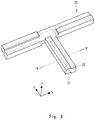
- FIG. 8A shows another example of a cross-sectional shape of a ridge waveguide according to the second embodiment of the present invention.
- FIG. 8B shows another example of a cross-sectional shape of a ridge waveguide according to the second embodiment of the present invention.
- FIG. 8D shows another example of a cross-sectional shape of a ridge waveguide according to the second embodiment of the present invention.
- FIG. 8E is a view showing another example of the cross-sectional shape of the ridge waveguide according to the second embodiment of the present invention.
- FIG. 9 shows a T-branch circuit of an S-shaped ridge waveguide according to a third embodiment of the present invention.
- FIG. 10A is a diagram for explaining a step structure of the S-shaped ridge waveguide shown in FIG. 9 ;
- FIG. 10B is a diagram for explaining a step structure of the S-shaped ridge waveguide shown in FIG. 9 ;
- FIG. 11 shows an example of a feeder circuit having a tournament structure in related art
- FIG. 12 shows a T-branch circuit of a normal ridge waveguide
- FIG. 13 shows a cross-sectional shape of the normal ridge waveguide shown in FIG. 12 ;
- FIG. 14 is an image diagram showing a cross-sectional shape of the normal ridge waveguide shown in FIG. 12 when the normal ridge waveguide is manufactured by using a thin-plate laminating method.
- FIG. 1 shows a T-branch circuit of a ridge waveguide 10 according to a first embodiment of the present invention.
- the ridge waveguide 10 is a ridge waveguide constituting a feeder circuit of an array antenna. Further, the ridge waveguide 10 includes a ridge part 11 .
- FIG. 2 shows a cross-sectional ape of the ridge waveguide 10 taken along a line 11 - 11 in FIG. 1 .
- the II-II cross-sectional shape of the ridge waveguide 10 is composed of sides 12 and 14 in a long-side direction (an X-direction), sides 13 and 15 in a short-side direction (a Z-direction), and the ridge part 11 . Further, the ridge part 11 is in contact with both the side 14 in the long-side direction and the side 15 in the short-side direction.
- a cutoff frequency of the ridge waveguide 10 is determined according to a length a 1 in the X-direction of the side 12 in the long-side direction, a length b 1 in the X-direction of the ridge part 11 , a length b 2 in the Z-direction of the ridge part 11 , and a length b 3 in the X-direction of the side 14 in the long-side direction.
- the lower the length a 1 is, the more the cutoff frequency of the ridge waveguide 10 can be made.
- the longer a value obtained by adding b 1 , b 2 and b 3 is, the lower the cutoff frequency of the ridge waveguide 10 can be made.
- the length b 1 in the X-direction and the length b 2 in the Z-direction of the ridge part 11 may be adjusted according to the value of the specified band.
- the side 14 in the long-side direction of the ridge waveguide 10 in the II-II cross-sectional shape differs from the two divided adjacent parts 118 and 119 of the ridge part 111 shown in FIG. 13 . Therefore, it is possible to make the length in the X-direction of the side 14 in the long-side direction longer than the length in the X-direction of each of the adjacent parts 118 and 119 of the ridge part 111 .
- FIG. 3 is an image diagram showing the II-II cross-sectional shape of the ridge waveguide 10 when it is manufactured by using a thin-plate laminating method.
- the ridge part 11 is formed by a part of each of thin plates 16 to 18 . That is, the ridge part 11 is not separated from the thin plates 16 to 18 . Therefore, the ridge waveguide 10 can be formed as a waveguide having a structure in which thin-plate metals are laminated, or a structure in which metal-plated printed circuit boards are laminated. That is, the ridge waveguide 10 can be manufactured by using the thin-plate laminating method.
- FIGS. 1 to 3 is explained on the assumption that the ridge part 11 is positioned in a lower-left part in the II-II cross-sectional shape of the ridge waveguide 10 , i.e., in a place where the ridge part 11 is in contact with both the side 14 in the long-side direction and the side 15 in the short-side direction.
- the position of the ridge part 11 is not limited to the above-described position.
- the ridge part 11 may be positioned in a place where the ridge part 11 is in contact with both the side 12 in the long-side direction and the side 13 in the short-side direction, a place where the ridge part 11 is in contact with both the side 14 in the long-side direction and the side 13 in the short-side direction, or a place where the ridge part 11 is in contact with both the side 12 in the long-side direction and the side 15 in the short-side direction.
- the ridge waveguide 10 may include a plurality of ridge parts.
- each of the plurality of ridge parts may be positioned in a place where the ridge part is in contact with both a side in the long-side direction and a side in the short-side direction.
- the ridge waveguide 10 includes a ridge part that is in contact with both a side in the long-side direction and a side in the short-side direction in the cross-sectional shape in the ridge waveguide.
- the ridge waveguide 10 can be manufactured by using the thin-plate laminating method.
- the ridge waveguide 10 it is possible to make the length in the X-direction of the side in the long-side direction that is in contact with the ridge part longer than the length in the X-direction of each of the adjacent parts 118 and 119 of the ridge part 111 shown in FIG. 13 .
- the ridge waveguide 10 it is possible to, when a cutting process is performed, easily perform the cutting process by using a drill as compared to the cutting process in the normal ridge waveguide 110 .
- the structure of the ridge waveguide 10 according to the first embodiment of the present invention it is possible to provide a ridge waveguide that can be easily manufactured.
- FIG. 4 shows a T-branch circuit of an S-shaped ridge waveguide 20 according to a second embodiment of the present invention.
- the S-shaped ridge waveguide 20 includes a ridge part 21 and a ridge part 22 . Note that in the S-shaped ridge waveguide 20 , the ridge parts 21 and 22 are arranged so that a cross-sectional shape of the S-shaped ridge waveguide 20 taken along a line V-V becomes an S-shape.
- FIG. 5 shows the V-V cross-sectional shape of the S-shaped ridge waveguide 20 shown in FIG. 4 .
- the V-V cross-sectional shape of the S-shaped ridge waveguide 20 is composed of sides 23 and 25 in a long-side direction (an X-direction), sides 24 and 26 in a short-side direction (a Z-direction), and the ridge parts 21 and 22 . Further, the ridge part 21 is in contact with both the side 25 in the long-side direction and the side 26 in the short-side direction. Further, the ridge part 22 is in contact with both the side 23 in the long-side direction and the side 24 in the short-side direction.
- a cutoff frequency of the S-shaped ridge waveguide 20 is determined according to a length c 1 in the X-direction of the side 23 in the long-side direction, a length c 2 in the Z-direction of the ridge part 22 , a length c 3 in the X-direction of the ridge part 22 , a length d 1 in the X-direction of the ridge part 21 , a length d 2 in the Z-direction of the ridge part 21 , and a length d 3 in the X-direction of the side 25 in the long-side direction.
- FIG. 6 is an image diagram showing the V-V cross-sectional shape of the S-shaped ridge waveguide 20 when it is manufactured by using a thin-plate laminating method.
- the ridge part 21 is formed by a part of each of thin plates 27 and 28 . That is, the ridge part 21 is not separated from the thin plates 27 and 28 .
- the ridge part 22 is formed by a part of each of thin plates 29 and 30 . That is, the ridge part 22 is not separated from the thin plates 29 and 30 . Therefore, the S-shaped ridge waveguide 20 can be formed as a waveguide having a structure in which thin-plate metals are laminated, or a structure in which metal-plated printed circuit boards are laminated. That is, the S-shaped ridge waveguide 20 can be manufactured by using the thin-plate laminating method.
- an element tube means a rectangular waveguide that differs from a ridge waveguide.
- FIG. 7 shows frequency characteristics of pass losses in an element tube, a normal ridge waveguide, and an S-shaped ridge waveguide, in each of which the length of the longest part in the long-side direction in its cross-sectional shape is adjusted to about 80% of the size of the standard waveguide.
- the normal ridge waveguide it is possible to lower the cutoff frequency of the S-shaped ridge waveguide as compared to the cutoff frequency of the element tube.
- the ridge parts 21 and 22 are arranged so that the V-V cross-sectional shape of the S-shaped ridge waveguide 20 becomes an S shape.
- the S-shaped ridge waveguide 20 is described as an example of a ridge waveguide including a plurality of ridges.
- the ridge waveguide including a plurality of ridges is not limited to those having the above-described cross-sectional shape.
- ridge waveguides having cross-sectional shapes shown in FIGS. 8A to 8E may be used.
- the third embodiment is a modified example of the second embodiment.
- descriptions of components and structures similar to those in the second embodiment are omitted as appropriate.
- FIG. 9 shows a T-branch circuit of an S-shaped ridge waveguide 40 according to the third embodiment of the present invention.
- the S-shaped ridge waveguide 40 includes ridge parts 41 and 42 , and step structures 43 and 44 . Note that the ridge parts 41 and 42 are similar to the ridge parts 21 and 22 of the second embodiment, and therefore descriptions thereof are omitted.
- FIG. 10B shows a cross-sectional shape of the S-shaped ridge waveguide 40 taken along a line XB-XB in FIG. 9 .
- FIG. 10A shows a cross-sectional shape of an S-shaped ridge waveguide that does not include the step structures 43 and 44 for a comparison to the cross-sectional shape shown in FIG. 10B .
- the S-shaped ridge waveguide shown in FIG. 10A does not include the step structures 43 and 44 . That is, the S-shaped ridge waveguide shown in FIG. 10A has a structure in which, in the tube-axial direction, there is only one step between the branch center of the T-branch circuit and the S-shaped structure.
- the S-shaped ridge waveguide 40 shown in FIG. 10B includes the step structures 43 and 44 in the tube-axial direction.
- the S-shaped ridge waveguide 40 includes two-step step structures 43 and 44 in the tube-axis direction.
- the S-shaped ridge waveguide 40 has a structure in which there are two steps between the branch center 45 of the T-branch circuit and the S-shaped structure 46 . Therefore, in the S-shaped ridge waveguide 40 , it is possible to smoothly convert an impedance between the branch center 45 and the S-shaped structure 46 as compared to the structure shown in FIG. 10A .
- each of the step structures 43 and 44 of the S-shaped ridge waveguide 40 is formed as a two-step step structure.
- the step structure is not limited to this structure and may be a step structure including three steps or more. That is, each of the step structures 43 and 44 may include n steps (n is an integer no less than two).
- the S-shaped ridge waveguide 40 includes the step structures 43 and 44 in the tube-axis direction. As a result, in the S-shaped ridge waveguide 40 , it is possible to smoothly convert the impedance between the branch center 45 and the S-shaped structure 46 .
- the S-shaped ridge waveguide 40 including the step structures 43 and 44 in the tube-axis direction is described.
- the structure of the S-shaped ridge waveguide is not limited to this structure.
- the ridge waveguide 10 according to the first embodiment may have a structure including step structures 43 and 44 in the tube axis direction.
Landscapes
- Engineering & Computer Science (AREA)
- Manufacturing & Machinery (AREA)
- Waveguides (AREA)
Abstract
Description
- 10 RIDGE WAVEGUIDE
- 11 RIDGE PART
- 14 SIDE IN LONG-SIDE DIRECTION
- 15 SIDE IN SHORT-SIDE DIRECTION
- 20 S-SHAPED RIDGE WAVEGUIDE
- 21, 22 RIDGE PART
- 23, 25 SIDE IN LONG-SIDE DIRECTION
- 24, 26 SIDE IN SHORT-SIDE DIRECTION
- 40 S-SHAPED RIDGE WAVEGUIDE
- 41, 42 RIDGE PART
- 43, 44 STEP STRUCTURE
Claims (5)
Applications Claiming Priority (3)
| Application Number | Priority Date | Filing Date | Title |
|---|---|---|---|
| JP2016072424 | 2016-03-31 | ||
| JP2016-072424 | 2016-03-31 | ||
| PCT/JP2017/004795 WO2017169165A1 (en) | 2016-03-31 | 2017-02-09 | Ridge waveguide and array antenna device |
Publications (2)
| Publication Number | Publication Date |
|---|---|
| US20190089035A1 US20190089035A1 (en) | 2019-03-21 |
| US10826148B2 true US10826148B2 (en) | 2020-11-03 |
Family
ID=59963819
Family Applications (1)
| Application Number | Title | Priority Date | Filing Date |
|---|---|---|---|
| US16/088,292 Active 2037-03-26 US10826148B2 (en) | 2016-03-31 | 2017-02-09 | Ridge waveguide and array antenna apparatus |
Country Status (2)
| Country | Link |
|---|---|
| US (1) | US10826148B2 (en) |
| WO (1) | WO2017169165A1 (en) |
Cited By (1)
| Publication number | Priority date | Publication date | Assignee | Title |
|---|---|---|---|---|
| US20230318200A1 (en) * | 2022-03-30 | 2023-10-05 | Gm Cruise Holdings Llc | Phase compensated power divider for a vertical polarized three-dimensional (3d) antenna |
Families Citing this family (8)
| Publication number | Priority date | Publication date | Assignee | Title |
|---|---|---|---|---|
| CN107749508B (en) * | 2017-11-21 | 2020-05-05 | 江苏贝孚德通讯科技股份有限公司 | Single ridge waveguide low pass filter and waveguide duplexer |
| WO2019203902A2 (en) | 2017-12-20 | 2019-10-24 | Optisys, LLC | Integrated tracking antenna array |
| CN109066045B (en) * | 2018-08-01 | 2021-02-19 | 中国航空工业集团公司雷华电子技术研究所 | Ridge waveguide broadband phase compensation structure |
| CN109346851B (en) * | 2018-09-28 | 2021-01-19 | 厦门大学 | Hollow pole wall waveguide slot array antenna based on 3D printing and metal coating |
| CN110518322A (en) * | 2019-09-24 | 2019-11-29 | 广州安波通信科技有限公司 | A kind of two road ridge waveguide power splitter of ultra wide band |
| EP4229718A4 (en) | 2020-10-19 | 2024-09-11 | Optisys, Inc. | BROADBAND WAVEGUIDE TO DUAL COAXIAL TRANSITION |
| WO2022094325A1 (en) | 2020-10-29 | 2022-05-05 | Optisys, Inc. | Integrated balanced radiating elements |
| US12009596B2 (en) | 2021-05-14 | 2024-06-11 | Optisys, Inc. | Planar monolithic combiner and multiplexer for antenna arrays |
Citations (7)
| Publication number | Priority date | Publication date | Assignee | Title |
|---|---|---|---|---|
| US3157847A (en) | 1961-07-11 | 1964-11-17 | Robert M Williams | Multilayered waveguide circuitry formed by stacking plates having surface grooves |
| WO2007114007A1 (en) | 2006-03-31 | 2007-10-11 | Nec Corporation | Waveguide coupler |
| US20120243823A1 (en) * | 2011-03-22 | 2012-09-27 | Giboney Kirk S | Gap-Mode Waveguide |
| US20130321229A1 (en) | 2011-02-17 | 2013-12-05 | Huber+Suhner Ag | Array antenna |
| JP2014170989A (en) | 2013-03-01 | 2014-09-18 | Tokyo Institute Of Technology | Slot array antenna, design method and manufacturing method |
| US9343795B1 (en) * | 2013-07-29 | 2016-05-17 | Sandia Corporation | Wideband unbalanced waveguide power dividers and combiners |
| US20180198215A1 (en) * | 2014-03-18 | 2018-07-12 | Lockheed Martin Corporation | Rf module with integrated waveguide and attached antenna elements and method for fabrication |
-
2017
- 2017-02-09 US US16/088,292 patent/US10826148B2/en active Active
- 2017-02-09 WO PCT/JP2017/004795 patent/WO2017169165A1/en not_active Ceased
Patent Citations (8)
| Publication number | Priority date | Publication date | Assignee | Title |
|---|---|---|---|---|
| US3157847A (en) | 1961-07-11 | 1964-11-17 | Robert M Williams | Multilayered waveguide circuitry formed by stacking plates having surface grooves |
| WO2007114007A1 (en) | 2006-03-31 | 2007-10-11 | Nec Corporation | Waveguide coupler |
| US20130321229A1 (en) | 2011-02-17 | 2013-12-05 | Huber+Suhner Ag | Array antenna |
| US20120243823A1 (en) * | 2011-03-22 | 2012-09-27 | Giboney Kirk S | Gap-Mode Waveguide |
| WO2012128866A1 (en) | 2011-03-22 | 2012-09-27 | Giboney Kirk S | Gap-mode waveguide |
| JP2014170989A (en) | 2013-03-01 | 2014-09-18 | Tokyo Institute Of Technology | Slot array antenna, design method and manufacturing method |
| US9343795B1 (en) * | 2013-07-29 | 2016-05-17 | Sandia Corporation | Wideband unbalanced waveguide power dividers and combiners |
| US20180198215A1 (en) * | 2014-03-18 | 2018-07-12 | Lockheed Martin Corporation | Rf module with integrated waveguide and attached antenna elements and method for fabrication |
Non-Patent Citations (2)
| Title |
|---|
| Alireza Mallahzadeh et al., "A Low Cross-Polarization Slotted Ridged SIW Array Antenna Design With Mutual Coupling Considerations", IEEE Transactions on Antennas and Propagation, Oct. 2015, pp. 4324-4333, vol. 63, No. 10. |
| International Search Report of PCT/JP2017/004795 dated Apr. 25, 2017 [PCT/ISA/210]. |
Cited By (2)
| Publication number | Priority date | Publication date | Assignee | Title |
|---|---|---|---|---|
| US20230318200A1 (en) * | 2022-03-30 | 2023-10-05 | Gm Cruise Holdings Llc | Phase compensated power divider for a vertical polarized three-dimensional (3d) antenna |
| US12100897B2 (en) * | 2022-03-30 | 2024-09-24 | Gm Cruise Holdings Llc | Phase compensated power divider for a vertical polarized three-dimensional (3D) antenna |
Also Published As
| Publication number | Publication date |
|---|---|
| US20190089035A1 (en) | 2019-03-21 |
| WO2017169165A1 (en) | 2017-10-05 |
Similar Documents
| Publication | Publication Date | Title |
|---|---|---|
| US10826148B2 (en) | Ridge waveguide and array antenna apparatus | |
| US9698487B2 (en) | Array antenna | |
| US10971824B2 (en) | Antenna element | |
| US9590304B2 (en) | Broadband antenna | |
| EP2765651A1 (en) | Antenna module and method for maufacturing the same | |
| US10862212B2 (en) | Antenna device and wireless communication device | |
| US10461439B2 (en) | Flexible polymer antenna with multiple ground resonators | |
| JP6340690B2 (en) | Antenna device | |
| US12206169B2 (en) | Antenna module | |
| CN103378420A (en) | Antenna system | |
| US20230352824A1 (en) | Antenna module and communication device including the same | |
| Karthikeya et al. | A wideband conformal antenna with high pattern integrity for mmWave 5G smartphones | |
| US7102573B2 (en) | Patch antenna | |
| US12394904B2 (en) | Metasurface for smartphone antenna, and smartphone device comprising same | |
| US20240106106A1 (en) | Antenna module and communication device equipped with the antenna module | |
| WO2018074056A1 (en) | Antenna device | |
| US11038248B2 (en) | Apparatus forming a strip line and dielectric part | |
| US12261368B2 (en) | Antenna device and communication device | |
| US11721908B2 (en) | Antenna structure with wide beamwidth | |
| CN219534865U (en) | Dual-frenquency millimeter wave antenna module and electronic equipment | |
| US10615493B2 (en) | Antenna structure | |
| US12597711B2 (en) | Antenna device and wireless terminal | |
| CN112909527A (en) | High-gain anti-sufficient Vivaldi antenna | |
| KR102713318B1 (en) | Wide angle microstrip patch antenna using gap-coupling with parasitic antenna | |
| US20250112373A1 (en) | Antenna device, communication device, and method for manufacturing antenna device |
Legal Events
| Date | Code | Title | Description |
|---|---|---|---|
| AS | Assignment |
Owner name: NEC CORPORATION, JAPAN Free format text: ASSIGNMENT OF ASSIGNORS INTEREST;ASSIGNOR:TAKAHASHI, YOSHIHIDE;REEL/FRAME:046965/0493 Effective date: 20180906 |
|
| FEPP | Fee payment procedure |
Free format text: ENTITY STATUS SET TO UNDISCOUNTED (ORIGINAL EVENT CODE: BIG.); ENTITY STATUS OF PATENT OWNER: LARGE ENTITY |
|
| STPP | Information on status: patent application and granting procedure in general |
Free format text: APPLICATION DISPATCHED FROM PREEXAM, NOT YET DOCKETED |
|
| STPP | Information on status: patent application and granting procedure in general |
Free format text: DOCKETED NEW CASE - READY FOR EXAMINATION |
|
| STPP | Information on status: patent application and granting procedure in general |
Free format text: NON FINAL ACTION MAILED |
|
| STPP | Information on status: patent application and granting procedure in general |
Free format text: RESPONSE TO NON-FINAL OFFICE ACTION ENTERED AND FORWARDED TO EXAMINER |
|
| STPP | Information on status: patent application and granting procedure in general |
Free format text: NOTICE OF ALLOWANCE MAILED -- APPLICATION RECEIVED IN OFFICE OF PUBLICATIONS |
|
| STPP | Information on status: patent application and granting procedure in general |
Free format text: PUBLICATIONS -- ISSUE FEE PAYMENT VERIFIED |
|
| STCF | Information on status: patent grant |
Free format text: PATENTED CASE |
|
| CC | Certificate of correction | ||
| MAFP | Maintenance fee payment |
Free format text: PAYMENT OF MAINTENANCE FEE, 4TH YEAR, LARGE ENTITY (ORIGINAL EVENT CODE: M1551); ENTITY STATUS OF PATENT OWNER: LARGE ENTITY Year of fee payment: 4 |