US10825927B2 - LDMOS device having hot carrier suppression - Google Patents
LDMOS device having hot carrier suppression Download PDFInfo
- Publication number
- US10825927B2 US10825927B2 US16/184,015 US201816184015A US10825927B2 US 10825927 B2 US10825927 B2 US 10825927B2 US 201816184015 A US201816184015 A US 201816184015A US 10825927 B2 US10825927 B2 US 10825927B2
- Authority
- US
- United States
- Prior art keywords
- region
- diffusion region
- conductivity type
- diffusion
- contact region
- Prior art date
- Legal status (The legal status is an assumption and is not a legal conclusion. Google has not performed a legal analysis and makes no representation as to the accuracy of the status listed.)
- Active
Links
Images


Classifications
-
- H01L29/7816—
-
- H—ELECTRICITY
- H10—SEMICONDUCTOR DEVICES; ELECTRIC SOLID-STATE DEVICES NOT OTHERWISE PROVIDED FOR
- H10D—INORGANIC ELECTRIC SEMICONDUCTOR DEVICES
- H10D30/00—Field-effect transistors [FET]
- H10D30/60—Insulated-gate field-effect transistors [IGFET]
- H10D30/64—Double-diffused metal-oxide semiconductor [DMOS] FETs
- H10D30/65—Lateral DMOS [LDMOS] FETs
-
- H01L29/063—
-
- H01L29/0634—
-
- H01L29/0653—
-
- H01L29/0865—
-
- H01L29/0878—
-
- H01L29/0882—
-
- H01L29/1083—
-
- H01L29/41758—
-
- H01L29/42356—
-
- H01L29/66681—
-
- H—ELECTRICITY
- H10—SEMICONDUCTOR DEVICES; ELECTRIC SOLID-STATE DEVICES NOT OTHERWISE PROVIDED FOR
- H10D—INORGANIC ELECTRIC SEMICONDUCTOR DEVICES
- H10D30/00—Field-effect transistors [FET]
- H10D30/01—Manufacture or treatment
- H10D30/021—Manufacture or treatment of FETs having insulated gates [IGFET]
- H10D30/028—Manufacture or treatment of FETs having insulated gates [IGFET] of double-diffused metal oxide semiconductor [DMOS] FETs
- H10D30/0281—Manufacture or treatment of FETs having insulated gates [IGFET] of double-diffused metal oxide semiconductor [DMOS] FETs of lateral DMOS [LDMOS] FETs
-
- H—ELECTRICITY
- H10—SEMICONDUCTOR DEVICES; ELECTRIC SOLID-STATE DEVICES NOT OTHERWISE PROVIDED FOR
- H10D—INORGANIC ELECTRIC SEMICONDUCTOR DEVICES
- H10D62/00—Semiconductor bodies, or regions thereof, of devices having potential barriers
- H10D62/10—Shapes, relative sizes or dispositions of the regions of the semiconductor bodies; Shapes of the semiconductor bodies
- H10D62/102—Constructional design considerations for preventing surface leakage or controlling electric field concentration
- H10D62/103—Constructional design considerations for preventing surface leakage or controlling electric field concentration for increasing or controlling the breakdown voltage of reverse-biased devices
- H10D62/105—Constructional design considerations for preventing surface leakage or controlling electric field concentration for increasing or controlling the breakdown voltage of reverse-biased devices by having particular doping profiles, shapes or arrangements of PN junctions; by having supplementary regions, e.g. junction termination extension [JTE]
- H10D62/109—Reduced surface field [RESURF] PN junction structures
- H10D62/111—Multiple RESURF structures, e.g. double RESURF or 3D-RESURF structures
-
- H—ELECTRICITY
- H10—SEMICONDUCTOR DEVICES; ELECTRIC SOLID-STATE DEVICES NOT OTHERWISE PROVIDED FOR
- H10D—INORGANIC ELECTRIC SEMICONDUCTOR DEVICES
- H10D62/00—Semiconductor bodies, or regions thereof, of devices having potential barriers
- H10D62/10—Shapes, relative sizes or dispositions of the regions of the semiconductor bodies; Shapes of the semiconductor bodies
- H10D62/113—Isolations within a component, i.e. internal isolations
- H10D62/115—Dielectric isolations, e.g. air gaps
- H10D62/116—Dielectric isolations, e.g. air gaps adjoining the input or output regions of field-effect devices, e.g. adjoining source or drain regions
-
- H—ELECTRICITY
- H10—SEMICONDUCTOR DEVICES; ELECTRIC SOLID-STATE DEVICES NOT OTHERWISE PROVIDED FOR
- H10D—INORGANIC ELECTRIC SEMICONDUCTOR DEVICES
- H10D62/00—Semiconductor bodies, or regions thereof, of devices having potential barriers
- H10D62/10—Shapes, relative sizes or dispositions of the regions of the semiconductor bodies; Shapes of the semiconductor bodies
- H10D62/13—Semiconductor regions connected to electrodes carrying current to be rectified, amplified or switched, e.g. source or drain regions
- H10D62/149—Source or drain regions of field-effect devices
- H10D62/151—Source or drain regions of field-effect devices of IGFETs
- H10D62/152—Source regions of DMOS transistors
- H10D62/154—Dispositions
-
- H—ELECTRICITY
- H10—SEMICONDUCTOR DEVICES; ELECTRIC SOLID-STATE DEVICES NOT OTHERWISE PROVIDED FOR
- H10D—INORGANIC ELECTRIC SEMICONDUCTOR DEVICES
- H10D62/00—Semiconductor bodies, or regions thereof, of devices having potential barriers
- H10D62/10—Shapes, relative sizes or dispositions of the regions of the semiconductor bodies; Shapes of the semiconductor bodies
- H10D62/13—Semiconductor regions connected to electrodes carrying current to be rectified, amplified or switched, e.g. source or drain regions
- H10D62/149—Source or drain regions of field-effect devices
- H10D62/151—Source or drain regions of field-effect devices of IGFETs
- H10D62/156—Drain regions of DMOS transistors
- H10D62/157—Impurity concentrations or distributions
-
- H—ELECTRICITY
- H10—SEMICONDUCTOR DEVICES; ELECTRIC SOLID-STATE DEVICES NOT OTHERWISE PROVIDED FOR
- H10D—INORGANIC ELECTRIC SEMICONDUCTOR DEVICES
- H10D62/00—Semiconductor bodies, or regions thereof, of devices having potential barriers
- H10D62/10—Shapes, relative sizes or dispositions of the regions of the semiconductor bodies; Shapes of the semiconductor bodies
- H10D62/13—Semiconductor regions connected to electrodes carrying current to be rectified, amplified or switched, e.g. source or drain regions
- H10D62/149—Source or drain regions of field-effect devices
- H10D62/151—Source or drain regions of field-effect devices of IGFETs
- H10D62/156—Drain regions of DMOS transistors
- H10D62/158—Dispositions
-
- H—ELECTRICITY
- H10—SEMICONDUCTOR DEVICES; ELECTRIC SOLID-STATE DEVICES NOT OTHERWISE PROVIDED FOR
- H10D—INORGANIC ELECTRIC SEMICONDUCTOR DEVICES
- H10D62/00—Semiconductor bodies, or regions thereof, of devices having potential barriers
- H10D62/10—Shapes, relative sizes or dispositions of the regions of the semiconductor bodies; Shapes of the semiconductor bodies
- H10D62/17—Semiconductor regions connected to electrodes not carrying current to be rectified, amplified or switched, e.g. channel regions
- H10D62/351—Substrate regions of field-effect devices
- H10D62/357—Substrate regions of field-effect devices of FETs
- H10D62/364—Substrate regions of field-effect devices of FETs of IGFETs
- H10D62/371—Inactive supplementary semiconductor regions, e.g. for preventing punch-through, improving capacity effect or leakage current
-
- H—ELECTRICITY
- H10—SEMICONDUCTOR DEVICES; ELECTRIC SOLID-STATE DEVICES NOT OTHERWISE PROVIDED FOR
- H10D—INORGANIC ELECTRIC SEMICONDUCTOR DEVICES
- H10D64/00—Electrodes of devices having potential barriers
- H10D64/20—Electrodes characterised by their shapes, relative sizes or dispositions
- H10D64/23—Electrodes carrying the current to be rectified, amplified, oscillated or switched, e.g. sources, drains, anodes or cathodes
- H10D64/251—Source or drain electrodes for field-effect devices
- H10D64/257—Source or drain electrodes for field-effect devices for lateral devices wherein the source or drain electrodes are characterised by top-view geometrical layouts, e.g. interdigitated, semi-circular, annular or L-shaped electrodes
-
- H—ELECTRICITY
- H10—SEMICONDUCTOR DEVICES; ELECTRIC SOLID-STATE DEVICES NOT OTHERWISE PROVIDED FOR
- H10D—INORGANIC ELECTRIC SEMICONDUCTOR DEVICES
- H10D64/00—Electrodes of devices having potential barriers
- H10D64/20—Electrodes characterised by their shapes, relative sizes or dispositions
- H10D64/27—Electrodes not carrying the current to be rectified, amplified, oscillated or switched, e.g. gates
- H10D64/311—Gate electrodes for field-effect devices
- H10D64/411—Gate electrodes for field-effect devices for FETs
- H10D64/511—Gate electrodes for field-effect devices for FETs for IGFETs
- H10D64/512—Disposition of the gate electrodes, e.g. buried gates
Definitions
- the present invention relates to a semiconductor device, and more particularly, to a semiconductor device including an LDMOS.
- Shallow trench isolation is employed for element isolation in a microscopic process.
- STI is formed by the embedding of an insulating film in a trench formed in a substrate surface.
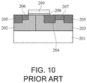
- the insulating film embedded in the trench is used not only for STI but also for the purpose of improving the withstand voltage of elements, and is employed in, for example, a semiconductor device illustrated in FIG. 10 which is an illustration of a semiconductor device including a laterally diffused metal oxide semiconductor (LDMOS) for a lateral high-withstand voltage MOS transistor (see FIG. 14 of Japanese Patent Application Laid-open No. 2014-107302, for example).
- LDMOS laterally diffused metal oxide semiconductor
- the LDMOS in the semiconductor device of the prior art includes an n-type diffusion region 202 and a p-type diffusion region 203 which are formed next to each other in a semiconductor substrate 201 , a p-type source contact region 206 which is formed in the n-type diffusion region 202 , a p-type drain contact region 207 which is formed in the p-type diffusion region 203 , a trench insulating region 204 which is formed next to the p-type drain contact region 207 in a portion of the p-type diffusion region 203 between the p-type source contact region 206 and the p-type drain contact region 207 , and a gate electrode 209 which is formed above the semiconductor substrate 201 through a gate insulating film 208 .
- the gate electrode 209 is formed so as to cover an area from an end portion of the p-type source contact region 206 on the p-type drain contact region 207 side to the top of the trench insulating region 204 .
- the LDMOS is isolated from other regions (not shown) by STI regions 205 .
- the arrival of a depletion layer which is generated from a junction portion between the n-type diffusion region 202 and the p-type diffusion region 203 , at a side wall of the trench insulating region 204 while the LDMOS is in operation increases the intensity of an electric field in the vicinity of the side wall, and the electric field increased in intensity accelerates carriers. Impact ionization consequently occurs in the vicinity of the side wall, and undesirably increases the possibility of hot carrier generation. While most of carriers (holes) including the generated hot carriers travel toward the drain contact region 207 , some carriers are attracted to an electric potential applied to the gate electrode 209 . An injection of the attracted carriers into the gate insulating film 208 leads to the breakdown of the gate insulating film 208 .
- a large number of defects due to a difference in thermal expansion coefficient between silicon serving as the substrate and the insulating film embedded in the trench, for example, a silicon oxide film, are found in the vicinity of side walls of the trench insulating region 204 .
- the defects are present also in a portion of the gate insulating film 208 in the vicinity of side walls of the trench insulating region 204 , and hence the portion of the gate insulating film 208 is vulnerable.
- the injection of some carriers described above readily occurs in the vulnerable portion of the gate insulating film 208 , with the result that the gate insulating film 208 breaks down.
- a semiconductor device including: a semiconductor substrate; a first diffusion region of a first conductivity type and a second diffusion region of a second conductivity type formed next to each other in the semiconductor substrate; a drain contact region of the first conductivity type formed in the first diffusion region; a source contact region of the first conductivity type formed in the second diffusion region; a trench insulating region formed in the first diffusion region between the drain contact region and the source contact region; a third diffusion region of the second conductivity type formed next to a side wall of the trench insulating region on the source contact region side in the first diffusion region between the source contact region and the trench insulating region; and a gate electrode formed on the semiconductor substrate through a gate insulating film so as to cover an area from an end portion of the source contact region on the drain contact region side to at least a part of a top surface of the trench insulating region.
- a depletion layer can be formed in advance in the first diffusion region. While the semiconductor device is in operation, the depletion layer formed in advance is joined by a depletion layer extending from a junction portion between the first diffusion region and the second diffusion region toward the drain contact region side. This enables the latter depletion layer to extend past the vicinity of the side wall of the trench insulating region to a neighborhood of the drain contact region.
- the intensity of an electric field in the vicinity of the side wall of the trench insulating region is thus lowered, and hence the acceleration of carriers in the vicinity of the side wall is reduced to a level lower than in the prior art and low enough to suppress the generation of hot carriers.
- the gate insulating film in the vicinity of the side wall of the trench insulating region is vulnerable as described above but, even when a few hot carriers are generated, the third diffusion region serving as an electric barrier against the hot carriers can prevent an injection of the hot carriers into the vulnerable portion found in the gate insulating film. The gate insulating film can thus be protected.
- FIG. 1 is a sectional view for illustrating the structure of a semiconductor device according to a first embodiment of the present invention
- FIG. 2A , FIG. 2B , and FIG. 2C are sectional views for illustrating the states of depletion layers during the operation of the semiconductor device according to the first embodiment of the present invention
- FIG. 3A and FIG. 3B are diagrams for illustrating the results of simulation for electric potential distribution in the semiconductor device according to the first embodiment of the present invention and a semiconductor device of the prior art while the semiconductor devices are in operation;
- FIGS. 4A and 4B are sectional views for illustrating steps in a manufacturing process of the semiconductor device according to the first embodiment of the present invention
- FIG. 5A , FIGS. 5B, and 5C are sectional views for illustrating steps in a manufacturing process of the semiconductor device according to the first embodiment of the present invention
- FIG. 6 is a sectional view for illustrating steps in a manufacturing process of the semiconductor device according to a second embodiment of the present invention.
- FIG. 7 is a sectional view for illustrating steps in a manufacturing process of the semiconductor device according to a third embodiment of the present invention.
- FIG. 8 is a sectional view for illustrating steps in a manufacturing process of the semiconductor device according to a fourth embodiment of the present invention.
- FIG. 9 is a sectional view for illustrating steps in a manufacturing process of the semiconductor device according to a fifth embodiment of the present invention.
- FIG. 10 is a sectional view for illustrating the configuration of the semiconductor device of the prior art.
- FIG. 1 is a sectional view for illustrating the structure of a semiconductor device according to a first embodiment of the present invention, in which an LDMOS is included.
- LDMOS p-channel LDMOS
- the LDMOS in the semiconductor device according to the first embodiment includes an n-type (a second conductivity type) diffusion region 102 and a p-type (a first conductivity type) diffusion region 103 which are formed next to each other in a semiconductor substrate 101 formed of p-type single-crystal silicon.
- a p-type source contact region 106 is formed in the n-type diffusion region 102
- a p-type drain contact region 107 is formed in the p-type diffusion region 103 .
- the p-type diffusion region 103 has the same polarity as that of the p-type drain contact region 107 , but is lower in impurity concentration than the p-type drain contact region 107 .
- a trench insulating region 104 is formed from, for example, a silicon oxide film in the p-type diffusion region 103 between the p-type source contact region 106 and the p-type drain contact region 107 so as to be in contact with the p-type drain contact region 107 .
- An n-type diffusion region 110 is formed in the p-type diffusion region 103 between the p-type source contact region 106 and the trench insulating region 104 so as to continuously cover the entirety of one side wall of the trench insulating region 104 and at least a part of a bottom surface of the trench insulating region 104 from an upper end portion of the trench insulating region 104 .
- a gate electrode 109 is formed on the semiconductor substrate 101 through a gate insulating film 108 .
- the gate electrode 109 covers an area from an end portion of the p-type source contact region 106 on the p-type drain contact region 107 side to a part of a top surface of the trench insulating region 104 so that the p-type source contact region 106 is on one side of the gate electrode 109 while the p-type drain contact region 107 is on the other side of the gate electrode 109 .
- the LDMOS in the semiconductor device according to the first embodiment is isolated from other regions (not shown) by STI regions 105 which are formed from, for example, silicon oxide films.
- the electric potential of the n-type diffusion region 110 is set to a floating potential when the semiconductor device according to the first embodiment is put into operation.
- a ground potential is applied to the p-type source contact region 106 (see FIG. 1 )
- an electric potential (e.g., ⁇ 2 V) lower than that of the p-type source contact region 106 is applied to the gate electrode 109
- an electric potential (e.g., ⁇ 36 V) lower than that of the gate electrode 109 is applied to the p-type drain contact region 107 (see FIG. 1 ).
- a depletion layer 131 spreads as an electric potential difference between the n-type diffusion region 102 and the p-type diffusion region 103 changes as illustrated in FIG. 2A .
- the n-type diffusion region 110 differs in polarity from the p-type diffusion region 103 , and a depletion layer 132 is accordingly formed in advance in a junction portion between the n-type diffusion region 110 and the p-type diffusion region 103 .
- the electric potential of the p-type drain contact region 107 is decreased further until the depletion layer 131 reaches the depletion layer 132 and joins the depletion layer 132 as illustrated in FIG. 2B .
- the depletion layer 131 cannot extend further in the place where the depletion layer 131 joins the depletion layer 132 , and accordingly extends downward below the depletion layer 132 .
- the depletion layer 131 and the depletion layer 132 extend further as one depletion layer 133 toward the p-type drain contact region 107 as illustrated in FIG. 2C .
- the forming of the n-type diffusion region 110 allows the depletion layer 133 to extend past a side wall portion of the trench insulating region 104 on the p-type source contact region 106 side toward the p-type drain contact region 107 side.
- the intensity of an electric field in the vicinity of the side wall portion is accordingly lessened to reduce carrier acceleration, and the generation of hot carriers is suppressed as a result.
- FIG. 3A is a diagram for illustrating the simulation result of electric potential distribution in the semiconductor device according to the first embodiment.
- FIG. 3B is a diagram for illustrating the simulation result of electric potential distribution in a semiconductor device of the prior art illustrated in FIG. 10 , as a comparative example.
- the ground potential is applied to the p-type source contact region 106
- an electric potential of ⁇ 2 V is applied to the gate electrode 109
- an electric potential of ⁇ 36 V is applied to the p-type drain contact region 107 .
- the generation of hot carriers can thus be suppressed in the vicinity of the side wall of the trench insulating region 104 , and the breakdown of the gate insulating film 108 due to the hot carriers is consequently prevented.
- the description given above deals with the suppression of hot carrier generation by the lessening of the intensity of the electric field between the p-type source contact region 106 and the p-type drain contact region 107 .
- the breakdown of the gate insulating film can be prevented in this case, too, in a manner described below.
- the n-type diffusion region 110 In the first embodiment, in which the n-type diffusion region 110 is provided next to the side wall of the trench insulating region 104 on the p-type source contact region 106 side, the n-type diffusion region 110 has a high electric potential due to the diffusion potential of the p-n junction. The holes accordingly detour around the n-type diffusion region 110 on their way to the gate insulating film 108 .
- the effect of protecting the gate insulating film 108 is obtained by suppressing the generation of hot carriers through the forming of the n-type diffusion region 110 as described above.
- the description of the semiconductor device according to the first embodiment uses an example in which the ground potential is applied to the p-type source contact region 106 , ⁇ 2 V is applied to the gate electrode 109 , and ⁇ 36 V is applied to the p-type drain contact region 107 , the condition about electric potentials to be applied is not limited to the example given above.
- FIG. 4A and FIG. 4B and FIG. 5A to FIG. 5C A method of manufacturing the semiconductor device of FIG. 1 is described next with reference to FIG. 4A and FIG. 4B and FIG. 5A to FIG. 5C .
- a trench 104 t for the trench insulating region and trenches 105 t for STI are formed first in a surface of the semiconductor substrate 101 as illustrated in FIG. 4A .
- the trenches 104 t and 105 t are formed by forming a silicon nitride film 121 first over the entire surface of the semiconductor substrate 101 , subsequently forming, through photolithography, a photoresist pattern (not shown) that has openings above regions in which the trenches 104 t and 105 t are to be formed, patterning the silicon nitride film 121 with the photoresist pattern as a mask, removing the photoresist pattern, and then etching the semiconductor substrate 101 with the patterned silicon nitride film 121 as a mask.
- a photoresist pattern 123 is then formed so as to have an opening above a region next to the side surface of the trench 104 t on the side of the p-type source contact region 106 (see FIG. 1 ) formed in a later step, and above at least a part of a region of the trench 104 t that is continuous from the former region as illustrated in FIG. 4B .
- an n-type impurity is implanted in the semiconductor substrate 101 by ion implantation as indicated by arrows 122 .
- the n-type diffusion region 110 which continuously covers the side surface of the trench 104 t and at least a part of the bottom surface of the trench 104 t in the semiconductor substrate 101 is formed in this manner.
- the photoresist pattern 123 is then removed by ashing treatment or other methods.
- a silicon oxide film for example, is formed by chemical vapor deposition (CVD) as an insulating film embedded in the trenches 104 t and 105 t and deposited on the semiconductor substrate 101 .
- the silicon nitride film 121 (see FIG. 4A and FIG. 4B ) is then used as a stopper to remove the silicon oxide film on the semiconductor substrate 101 by chemical mechanical polishing (CMP) for leveling.
- CMP chemical mechanical polishing
- the silicon nitride film 121 is then removed, thereby forming the trench insulating region 104 which is embedded in the trench 104 t , and the STI regions 105 which are embedded in the trenches 105 t , as illustrated in FIG. 5A .
- a photoresist pattern (not shown) is subsequently formed so as to have an opening above a region in which the n-type diffusion region 102 is formed as illustrated in FIG. 5B , and ion implantation of an n-type impurity is conducted.
- another photoresist pattern (not shown) is formed so as to have an opening above a region in which the p-type diffusion region 103 is formed, and ion implantation of a p-type impurity is conducted.
- Heat treatment is then performed to form the n-type diffusion region 102 and the p-type diffusion region 103 next to each other in the semiconductor substrate 101 .
- the gate insulating film 108 is formed by thermally oxidizing the surface of the semiconductor substrate 101 , and a polysilicon film, for example, is deposited on the gate insulating film 108 as a material of the gate electrode as illustrated in FIG. 5C .
- a photoresist pattern (not shown) is then formed so as to have an opening above a region in which the gate electrode is formed, and etching is conducted with the photoresist pattern as a mask.
- the gate electrode 109 and gate insulating film 108 patterned into desired shapes are formed in this manner.
- a p-type impurity is implanted by ion implantation in the entire surface, thereby forming the p-type source contact region 106 and the p-type drain contact region 107 through self-alignment.
- the semiconductor device according to the first embodiment illustrated in FIG. 1 is obtained through the steps described above.
- FIG. 6 is a sectional view for illustrating the structure of a semiconductor device according to a second embodiment of the present invention.
- the semiconductor device according to the second embodiment differs from that of the first embodiment in the extent of an area in which the n-type diffusion region 110 is formed.
- the n-type diffusion region 110 in the second embodiment is formed so as to cover at least a part of one side wall of the trench insulating region 104 including an upper end portion of the side wall.
- the n-type diffusion region 110 that is formed in this manner yields the effect of suppressing the generation of hot carriers. Even when a few hot carriers are generated, the effect of preventing an injection of the hot carriers (holes) into the vulnerable portion of the gate insulating film 108 is obtained since the electric potential of the n-type diffusion region 110 is high due to the diffusion potential of the p-n junction. The breakdown of the gate insulating film 108 is consequently prevented.
- the semiconductor device according to the first embodiment is somewhat superior to the semiconductor device according to the second embodiment in terms of the effect of suppressing hot carriers.
- the LDMOS in the semiconductor device according to the second embodiment has an advantage of being low in ON resistance. The reason is described below.
- Heat treatment is conducted to form the n-type diffusion region 110 and the p-type diffusion region 103 .
- the impurity of the n-type diffusion region 110 and the impurity of the p-type diffusion region 103 are both diffused, thereby raising the resistance of the p-type diffusion region 103 .
- the semiconductor device according to the first embodiment is wide in the extent of an area in which the n-type diffusion region 110 is formed, and is affected by the rise in resistance quite easily.
- the semiconductor device according to the second embodiment is hardly affected by the rise in resistance, and the ON resistance of the LDMOS can accordingly be made lower than that in the semiconductor device according to the first embodiment.
- FIG. 7 is a sectional view for illustrating the structure of a semiconductor device according to a third embodiment of the present invention.
- the semiconductor device according to the third embodiment differs from those of the first embodiment and the second embodiment in the extent of an area in which the n-type diffusion region 110 is formed.
- the n-type diffusion region 110 in the third embodiment is formed in a place apart from a side wall portion of the trench insulating region 104 .
- a part of the p-type diffusion region 103 is interposed between the n-type diffusion region 110 and a side wall of the trench insulating region 104 .
- the n-type diffusion region 110 is spaced apart from the side wall portion of the trench insulating region 104 , the electric potential of the n-type diffusion region 110 is high due to the diffusion potential, and the electric potential is high around the n-type diffusion region 110 as well. Accordingly, even when a few hot carriers are generated, hot carriers (holes) do not enter a region between the side wall of the trench insulating region 104 and the n-type diffusion region 110 .
- the breakdown of the gate insulating film 108 due to an injection of hot carriers into a vulnerable portion of the gate insulating film 108 is consequently prevented in the third embodiment as well.
- the effect of suppressing hot carrier generation can be obtained by forming the n-type diffusion region 110 in the vicinity of a side wall of the trench insulating region 104 as described above.
- the n-type diffusion region 110 therefore is not always required to cover the side wall portion of the trench insulating region 104 completely.
- the above-mentioned effect decreases when the n-type diffusion region 110 is too far from the side wall portion of the trench insulating region 104 , and hence it is desirable to suitably adjust the extent of an area in which the n-type diffusion region 110 is formed.
- the n-type diffusion region 110 in the second embodiment illustrated in FIG. 6 and the n-type diffusion region 110 in the third embodiment illustrated in FIG. 7 can be formed by suitably adjusting the position and size of the opening in the photoresist 123 , or suitably adjusting the energy of ion implantation in the process step shown by FIG. 4B which is a diagram for illustrating the process of forming the n-type diffusion region 110 in the first embodiment.
- FIG. 8 is a sectional view for illustrating the structure of a semiconductor device according to a fourth embodiment of the present invention.
- the semiconductor device according to the fourth embodiment differs from that of the first embodiment in that an n-type embedded layer 111 is formed below the n-type diffusion region 102 and the p-type diffusion region 103 in the semiconductor substrate 101 and spaced from the n-type diffusion region 102 and the p-type diffusion region 103 .
- the n-type embedded layer 111 is formed by, for example, implanting an n-type impurity by ion implantation at high energy before the trench insulating region 104 is formed.
- the n-type embedded layer 111 is electrically connected to the n-type diffusion region 102 .
- the p-type semiconductor substrate 101 and the LDMOS can electrically be isolated from each other in this manner.
- a depletion layer due to a p-n junction is formed between the n-type embedded layer 111 and the p-type diffusion region 103 .
- a reverse-biased relation is formed between the n-type embedded layer 111 and the p-type diffusion region 103 when the electric potential of the p-type drain contact region 107 is lowered, and the depletion layer consequently spreads between the two.
- the depletion layer 133 (see FIG. 2C ) does not reach a deep portion of the p-type semiconductor substrate 101 , and extends even further toward the p-type drain contact region 107 side. This means that, according to the fourth embodiment, the effect of lessening electric field intensity is expected to be even greater.
- FIG. 9 is a sectional view for illustrating the structure of a semiconductor device according to a fifth embodiment of the present invention.
- the semiconductor device differs from that of the first embodiment in that a p-type diffusion region 112 which has an impurity concentration higher than that of the p-type diffusion region 103 and lower than that of the p-type drain contact region 107 , is formed below the p-type drain contact region 107 .
- the p-type diffusion region 112 is formed by implanting a p-type impurity by ion implantation at energy higher than the energy used to form the p-type drain contact region 107 , after the p-type diffusion region 103 is formed.
- the p-type diffusion region 112 in the fifth embodiment is higher in impurity concentration than the p-type diffusion region 103 as described above. This makes it difficult for a depletion layer to spread into the p-type diffusion region 112 , thereby providing an effect of preventing the p-type drain contact region 107 from turning into a depleted region. An improvement in the withstand voltage of the semiconductor device can accordingly be expected.
- the p-type diffusion region 112 has a possibility of causing avalanche breakdown because of its high impurity concentration. It is therefore desirable to suitably adjust the impurity concentrations of the n-type diffusion region 110 and the p-type diffusion region 112 , and the extent of areas in which the n-type diffusion region 110 and the p-type diffusion region 112 are formed.
- an n-type semiconductor substrate may be employed and the conductivity type of the semiconductor substrate is not limited.
- the present invention is also applicable to an n-channel LDMOS other than the p-channel LDMOS described above as an example.
- the fourth embodiment and the fifth embodiment deal with an example in which the n-type embedded region 111 is added to the semiconductor device according to the first embodiment illustrated in FIG. 1 , and an example in which the p-type diffusion region 112 is added to the semiconductor device of FIG. 1 , respectively.
- the n-type embedded layer 111 and the p-type diffusion region 112 can be added to the semiconductor device according to the second embodiment and the semiconductor device according to the third embodiment as well.
- the semiconductor devices may also have a configuration in which the n-type embedded layer 111 and the p-type diffusion region 112 are both included.
Landscapes
- Insulated Gate Type Field-Effect Transistor (AREA)
- Chemical & Material Sciences (AREA)
- Composite Materials (AREA)
Abstract
Description
Claims (9)
Applications Claiming Priority (2)
| Application Number | Priority Date | Filing Date | Title |
|---|---|---|---|
| JP2017217346A JP6956600B2 (en) | 2017-11-10 | 2017-11-10 | Semiconductor device |
| JP2017-217346 | 2017-11-10 |
Publications (2)
| Publication Number | Publication Date |
|---|---|
| US20190148543A1 US20190148543A1 (en) | 2019-05-16 |
| US10825927B2 true US10825927B2 (en) | 2020-11-03 |
Family
ID=66432417
Family Applications (1)
| Application Number | Title | Priority Date | Filing Date |
|---|---|---|---|
| US16/184,015 Active US10825927B2 (en) | 2017-11-10 | 2018-11-08 | LDMOS device having hot carrier suppression |
Country Status (2)
| Country | Link |
|---|---|
| US (1) | US10825927B2 (en) |
| JP (1) | JP6956600B2 (en) |
Families Citing this family (2)
| Publication number | Priority date | Publication date | Assignee | Title |
|---|---|---|---|---|
| US11195947B2 (en) * | 2019-10-24 | 2021-12-07 | Globalfoundries U.S. Inc. | Semiconductor device with doped region adjacent isolation structure in extension region |
| CN112825327B (en) * | 2019-11-21 | 2024-10-01 | 中芯国际集成电路制造(上海)有限公司 | Semiconductor structure and method of forming the same |
Citations (6)
| Publication number | Priority date | Publication date | Assignee | Title |
|---|---|---|---|---|
| US20040251492A1 (en) * | 2003-06-13 | 2004-12-16 | John Lin | LDMOS transistors and methods for making the same |
| US20110220995A1 (en) * | 2010-03-10 | 2011-09-15 | Taiwan Semiconductor Manufacturing Company, Ltd. | Semiconductor Device Having Multi-Thickness Gate Dielectric |
| JP2014107302A (en) | 2012-11-22 | 2014-06-09 | Renesas Electronics Corp | Semiconductor device |
| US20150069509A1 (en) * | 2013-09-06 | 2015-03-12 | SK Hynix Inc. | Semiconductor device |
| US20150364598A1 (en) * | 2014-06-12 | 2015-12-17 | Semiconductor Manufacturing International (Shanghai) Corporation | Semiconductor device and fabrication method thereof |
| US20190058039A1 (en) * | 2017-08-21 | 2019-02-21 | Texas Instruments Incorporated | Integrated circuit, ldmos with trapezoid jfet, bottom gate and ballast drift and fabrication method |
Family Cites Families (7)
| Publication number | Priority date | Publication date | Assignee | Title |
|---|---|---|---|---|
| US7791161B2 (en) * | 2005-08-25 | 2010-09-07 | Freescale Semiconductor, Inc. | Semiconductor devices employing poly-filled trenches |
| JP5407398B2 (en) * | 2009-02-12 | 2014-02-05 | 富士電機株式会社 | Semiconductor device |
| US9159803B2 (en) * | 2012-08-21 | 2015-10-13 | Freescale Semiconductor, Inc. | Semiconductor device with HCI protection region |
| JP5887233B2 (en) * | 2012-09-10 | 2016-03-16 | ルネサスエレクトロニクス株式会社 | Semiconductor device and manufacturing method thereof |
| CN104282563A (en) * | 2013-07-03 | 2015-01-14 | 中芯国际集成电路制造(上海)有限公司 | LDMOS device and forming method thereof |
| JP6651957B2 (en) * | 2016-04-06 | 2020-02-19 | 株式会社デンソー | Semiconductor device and manufacturing method thereof |
| JP6707439B2 (en) * | 2016-11-21 | 2020-06-10 | ルネサスエレクトロニクス株式会社 | Semiconductor device and manufacturing method thereof |
-
2017
- 2017-11-10 JP JP2017217346A patent/JP6956600B2/en active Active
-
2018
- 2018-11-08 US US16/184,015 patent/US10825927B2/en active Active
Patent Citations (6)
| Publication number | Priority date | Publication date | Assignee | Title |
|---|---|---|---|---|
| US20040251492A1 (en) * | 2003-06-13 | 2004-12-16 | John Lin | LDMOS transistors and methods for making the same |
| US20110220995A1 (en) * | 2010-03-10 | 2011-09-15 | Taiwan Semiconductor Manufacturing Company, Ltd. | Semiconductor Device Having Multi-Thickness Gate Dielectric |
| JP2014107302A (en) | 2012-11-22 | 2014-06-09 | Renesas Electronics Corp | Semiconductor device |
| US20150069509A1 (en) * | 2013-09-06 | 2015-03-12 | SK Hynix Inc. | Semiconductor device |
| US20150364598A1 (en) * | 2014-06-12 | 2015-12-17 | Semiconductor Manufacturing International (Shanghai) Corporation | Semiconductor device and fabrication method thereof |
| US20190058039A1 (en) * | 2017-08-21 | 2019-02-21 | Texas Instruments Incorporated | Integrated circuit, ldmos with trapezoid jfet, bottom gate and ballast drift and fabrication method |
Also Published As
| Publication number | Publication date |
|---|---|
| JP6956600B2 (en) | 2021-11-02 |
| JP2019087707A (en) | 2019-06-06 |
| US20190148543A1 (en) | 2019-05-16 |
Similar Documents
| Publication | Publication Date | Title |
|---|---|---|
| US7161213B2 (en) | Low threshold voltage PMOS apparatus and method of fabricating the same | |
| US7687853B2 (en) | System and method for making a LDMOS device with electrostatic discharge protection | |
| US9786657B1 (en) | Semiconductor structure including a transistor including a gate electrode region provided in a substrate and method for the formation thereof | |
| US9660020B2 (en) | Integrated circuits with laterally diffused metal oxide semiconductor structures and methods for fabricating the same | |
| CN106972050B (en) | Local Self-Biased Isolation in Semiconductor Devices | |
| US9112025B2 (en) | LDMOS device and fabrication method | |
| US9899477B2 (en) | Edge termination structure having a termination charge region below a recessed field oxide region | |
| US20080067615A1 (en) | Semiconductor device and method for fabricating thereof | |
| US20060011985A1 (en) | Asymmetric hetero-doped high-voltage MOSFET (AH2MOS) | |
| US9230956B2 (en) | Junction field effect transistors and associated fabrication methods | |
| EP3611765B1 (en) | Method of fabricating a semiconductor device with latchup immunity | |
| US10062704B2 (en) | Buried-channel MOSFET and a surface-channel MOSFET of a same type and fabrication method thereof | |
| JP2012009545A (en) | Semiconductor device manufacturing method | |
| US9853099B1 (en) | Double diffused metal oxide semiconductor device and manufacturing method thereof | |
| US10910493B2 (en) | Semiconductor device and method of manufacturing the same | |
| US8269274B2 (en) | Semiconductor device and method for fabricating the same | |
| US10825927B2 (en) | LDMOS device having hot carrier suppression | |
| US20050263843A1 (en) | Semiconductor device and fabrication method therefor | |
| US20080087969A1 (en) | Planar-type semiconductor device and method of manufacturing the same | |
| US8907432B2 (en) | Isolated device and manufacturing method thereof | |
| CN101651104B (en) | Semiconductor device and method for manufacturing the same | |
| US9299833B2 (en) | Lateral double diffused MOSFET device | |
| US7488638B2 (en) | Method for fabricating a voltage-stable PMOSFET semiconductor structure | |
| TWI765111B (en) | Field effect transistor and method of making the same | |
| KR100587605B1 (en) | High voltage transistors and manufacturing method thereof |
Legal Events
| Date | Code | Title | Description |
|---|---|---|---|
| AS | Assignment |
Owner name: ABLIC INC., JAPAN Free format text: ASSIGNMENT OF ASSIGNORS INTEREST;ASSIGNORS:KOJIMA, RYUHEI;NAGAO, KEISUKE;REEL/FRAME:047452/0830 Effective date: 20181001 |
|
| FEPP | Fee payment procedure |
Free format text: ENTITY STATUS SET TO UNDISCOUNTED (ORIGINAL EVENT CODE: BIG.); ENTITY STATUS OF PATENT OWNER: LARGE ENTITY |
|
| STPP | Information on status: patent application and granting procedure in general |
Free format text: DOCKETED NEW CASE - READY FOR EXAMINATION |
|
| STPP | Information on status: patent application and granting procedure in general |
Free format text: NON FINAL ACTION MAILED |
|
| STPP | Information on status: patent application and granting procedure in general |
Free format text: RESPONSE TO NON-FINAL OFFICE ACTION ENTERED AND FORWARDED TO EXAMINER |
|
| STPP | Information on status: patent application and granting procedure in general |
Free format text: FINAL REJECTION MAILED |
|
| STPP | Information on status: patent application and granting procedure in general |
Free format text: NON FINAL ACTION MAILED |
|
| STPP | Information on status: patent application and granting procedure in general |
Free format text: NOTICE OF ALLOWANCE MAILED -- APPLICATION RECEIVED IN OFFICE OF PUBLICATIONS |
|
| STPP | Information on status: patent application and granting procedure in general |
Free format text: PUBLICATIONS -- ISSUE FEE PAYMENT VERIFIED |
|
| STCF | Information on status: patent grant |
Free format text: PATENTED CASE |
|
| AS | Assignment |
Owner name: ABLIC INC., JAPAN Free format text: CHANGE OF ADDRESS;ASSIGNOR:ABLIC INC.;REEL/FRAME:064021/0575 Effective date: 20230424 |
|
| MAFP | Maintenance fee payment |
Free format text: PAYMENT OF MAINTENANCE FEE, 4TH YEAR, LARGE ENTITY (ORIGINAL EVENT CODE: M1551); ENTITY STATUS OF PATENT OWNER: LARGE ENTITY Year of fee payment: 4 |