US10825914B2 - Manufacturing method of semiconductor device - Google Patents
Manufacturing method of semiconductor device Download PDFInfo
- Publication number
- US10825914B2 US10825914B2 US16/180,026 US201816180026A US10825914B2 US 10825914 B2 US10825914 B2 US 10825914B2 US 201816180026 A US201816180026 A US 201816180026A US 10825914 B2 US10825914 B2 US 10825914B2
- Authority
- US
- United States
- Prior art keywords
- substrate
- gate
- stack structures
- conductive layer
- dielectric layer
- Prior art date
- Legal status (The legal status is an assumption and is not a legal conclusion. Google has not performed a legal analysis and makes no representation as to the accuracy of the status listed.)
- Active
Links
Images


Classifications
-
- H01L29/66545—
-
- H—ELECTRICITY
- H10—SEMICONDUCTOR DEVICES; ELECTRIC SOLID-STATE DEVICES NOT OTHERWISE PROVIDED FOR
- H10D—INORGANIC ELECTRIC SEMICONDUCTOR DEVICES
- H10D64/00—Electrodes of devices having potential barriers
- H10D64/01—Manufacture or treatment
- H10D64/017—Manufacture or treatment using dummy gates in processes wherein at least parts of the final gates are self-aligned to the dummy gates, i.e. replacement gate processes
-
- H—ELECTRICITY
- H01—ELECTRIC ELEMENTS
- H01L—SEMICONDUCTOR DEVICES NOT COVERED BY CLASS H10
- H01L21/00—Processes or apparatus adapted for the manufacture or treatment of semiconductor or solid state devices or of parts thereof
- H01L21/02—Manufacture or treatment of semiconductor devices or of parts thereof
- H01L21/02104—Forming layers
- H01L21/02365—Forming inorganic semiconducting materials on a substrate
- H01L21/02367—Substrates
- H01L21/0237—Materials
- H01L21/02373—Group 14 semiconducting materials
- H01L21/02381—Silicon, silicon germanium, germanium
-
- H—ELECTRICITY
- H01—ELECTRIC ELEMENTS
- H01L—SEMICONDUCTOR DEVICES NOT COVERED BY CLASS H10
- H01L21/00—Processes or apparatus adapted for the manufacture or treatment of semiconductor or solid state devices or of parts thereof
- H01L21/02—Manufacture or treatment of semiconductor devices or of parts thereof
- H01L21/02104—Forming layers
- H01L21/02365—Forming inorganic semiconducting materials on a substrate
- H01L21/02518—Deposited layers
- H01L21/02521—Materials
- H01L21/02524—Group 14 semiconducting materials
- H01L21/02532—Silicon, silicon germanium, germanium
-
- H—ELECTRICITY
- H01—ELECTRIC ELEMENTS
- H01L—SEMICONDUCTOR DEVICES NOT COVERED BY CLASS H10
- H01L21/00—Processes or apparatus adapted for the manufacture or treatment of semiconductor or solid state devices or of parts thereof
- H01L21/02—Manufacture or treatment of semiconductor devices or of parts thereof
- H01L21/02104—Forming layers
- H01L21/02365—Forming inorganic semiconducting materials on a substrate
- H01L21/02612—Formation types
- H01L21/02617—Deposition types
- H01L21/02636—Selective deposition, e.g. simultaneous growth of mono- and non-monocrystalline semiconductor materials
- H01L21/02639—Preparation of substrate for selective deposition
-
- H—ELECTRICITY
- H01—ELECTRIC ELEMENTS
- H01L—SEMICONDUCTOR DEVICES NOT COVERED BY CLASS H10
- H01L21/00—Processes or apparatus adapted for the manufacture or treatment of semiconductor or solid state devices or of parts thereof
- H01L21/02—Manufacture or treatment of semiconductor devices or of parts thereof
- H01L21/04—Manufacture or treatment of semiconductor devices or of parts thereof the devices having potential barriers, e.g. a PN junction, depletion layer or carrier concentration layer
- H01L21/18—Manufacture or treatment of semiconductor devices or of parts thereof the devices having potential barriers, e.g. a PN junction, depletion layer or carrier concentration layer the devices having semiconductor bodies comprising elements of Group IV of the Periodic Table or AIIIBV compounds with or without impurities, e.g. doping materials
- H01L21/30—Treatment of semiconductor bodies using processes or apparatus not provided for in groups H01L21/20 - H01L21/26
- H01L21/31—Treatment of semiconductor bodies using processes or apparatus not provided for in groups H01L21/20 - H01L21/26 to form insulating layers thereon, e.g. for masking or by using photolithographic techniques; After treatment of these layers; Selection of materials for these layers
- H01L21/3105—After-treatment
- H01L21/31051—Planarisation of the insulating layers
- H01L21/31053—Planarisation of the insulating layers involving a dielectric removal step
- H01L21/31055—Planarisation of the insulating layers involving a dielectric removal step the removal being a chemical etching step, e.g. dry etching
-
- H—ELECTRICITY
- H01—ELECTRIC ELEMENTS
- H01L—SEMICONDUCTOR DEVICES NOT COVERED BY CLASS H10
- H01L21/00—Processes or apparatus adapted for the manufacture or treatment of semiconductor or solid state devices or of parts thereof
- H01L21/70—Manufacture or treatment of devices consisting of a plurality of solid state components formed in or on a common substrate or of parts thereof; Manufacture of integrated circuit devices or of parts thereof
- H01L21/71—Manufacture of specific parts of devices defined in group H01L21/70
- H01L21/76—Making of isolation regions between components
- H01L21/762—Dielectric regions, e.g. EPIC dielectric isolation, LOCOS; Trench refilling techniques, SOI technology, use of channel stoppers
- H01L21/76294—Dielectric regions, e.g. EPIC dielectric isolation, LOCOS; Trench refilling techniques, SOI technology, use of channel stoppers using selective deposition of single crystal silicon, i.e. SEG techniques
-
- H01L27/11546—
-
- H01L29/41783—
-
- H01L29/42328—
-
- H01L29/495—
-
- H01L29/6653—
-
- H—ELECTRICITY
- H10—SEMICONDUCTOR DEVICES; ELECTRIC SOLID-STATE DEVICES NOT OTHERWISE PROVIDED FOR
- H10B—ELECTRONIC MEMORY DEVICES
- H10B41/00—Electrically erasable-and-programmable ROM [EEPROM] devices comprising floating gates
- H10B41/40—Electrically erasable-and-programmable ROM [EEPROM] devices comprising floating gates characterised by the peripheral circuit region
- H10B41/42—Simultaneous manufacture of periphery and memory cells
- H10B41/49—Simultaneous manufacture of periphery and memory cells comprising different types of peripheral transistor
-
- H—ELECTRICITY
- H10—SEMICONDUCTOR DEVICES; ELECTRIC SOLID-STATE DEVICES NOT OTHERWISE PROVIDED FOR
- H10D—INORGANIC ELECTRIC SEMICONDUCTOR DEVICES
- H10D30/00—Field-effect transistors [FET]
- H10D30/60—Insulated-gate field-effect transistors [IGFET]
- H10D30/68—Floating-gate IGFETs
- H10D30/6891—Floating-gate IGFETs characterised by the shapes, relative sizes or dispositions of the floating gate electrode
- H10D30/6892—Floating-gate IGFETs characterised by the shapes, relative sizes or dispositions of the floating gate electrode having at least one additional gate other than the floating gate and the control gate, e.g. program gate, erase gate or select gate
-
- H—ELECTRICITY
- H10—SEMICONDUCTOR DEVICES; ELECTRIC SOLID-STATE DEVICES NOT OTHERWISE PROVIDED FOR
- H10D—INORGANIC ELECTRIC SEMICONDUCTOR DEVICES
- H10D64/00—Electrodes of devices having potential barriers
- H10D64/01—Manufacture or treatment
- H10D64/015—Manufacture or treatment removing at least parts of gate spacers, e.g. disposable spacers
-
- H—ELECTRICITY
- H10—SEMICONDUCTOR DEVICES; ELECTRIC SOLID-STATE DEVICES NOT OTHERWISE PROVIDED FOR
- H10D—INORGANIC ELECTRIC SEMICONDUCTOR DEVICES
- H10D64/00—Electrodes of devices having potential barriers
- H10D64/20—Electrodes characterised by their shapes, relative sizes or dispositions
- H10D64/23—Electrodes carrying the current to be rectified, amplified, oscillated or switched, e.g. sources, drains, anodes or cathodes
- H10D64/251—Source or drain electrodes for field-effect devices
- H10D64/258—Source or drain electrodes for field-effect devices characterised by the relative positions of the source or drain electrodes with respect to the gate electrode
- H10D64/259—Source or drain electrodes being self-aligned with the gate electrode and having bottom surfaces higher than the interface between the channel and the gate dielectric
-
- H—ELECTRICITY
- H10—SEMICONDUCTOR DEVICES; ELECTRIC SOLID-STATE DEVICES NOT OTHERWISE PROVIDED FOR
- H10D—INORGANIC ELECTRIC SEMICONDUCTOR DEVICES
- H10D64/00—Electrodes of devices having potential barriers
- H10D64/60—Electrodes characterised by their materials
- H10D64/66—Electrodes having a conductor capacitively coupled to a semiconductor by an insulator, e.g. MIS electrodes
- H10D64/665—Electrodes having a conductor capacitively coupled to a semiconductor by an insulator, e.g. MIS electrodes the conductor comprising a layer of elemental metal contacting the insulator, e.g. tungsten or molybdenum
-
- H10P14/271—
-
- H10P14/2905—
-
- H10P14/3411—
-
- H10P95/064—
-
- H10W10/018—
-
- H10W10/10—
-
- H—ELECTRICITY
- H01—ELECTRIC ELEMENTS
- H01L—SEMICONDUCTOR DEVICES NOT COVERED BY CLASS H10
- H01L21/00—Processes or apparatus adapted for the manufacture or treatment of semiconductor or solid state devices or of parts thereof
- H01L21/02—Manufacture or treatment of semiconductor devices or of parts thereof
- H01L21/04—Manufacture or treatment of semiconductor devices or of parts thereof the devices having potential barriers, e.g. a PN junction, depletion layer or carrier concentration layer
- H01L21/18—Manufacture or treatment of semiconductor devices or of parts thereof the devices having potential barriers, e.g. a PN junction, depletion layer or carrier concentration layer the devices having semiconductor bodies comprising elements of Group IV of the Periodic Table or AIIIBV compounds with or without impurities, e.g. doping materials
- H01L21/30—Treatment of semiconductor bodies using processes or apparatus not provided for in groups H01L21/20 - H01L21/26
- H01L21/31—Treatment of semiconductor bodies using processes or apparatus not provided for in groups H01L21/20 - H01L21/26 to form insulating layers thereon, e.g. for masking or by using photolithographic techniques; After treatment of these layers; Selection of materials for these layers
- H01L21/3205—Deposition of non-insulating-, e.g. conductive- or resistive-, layers on insulating layers; After-treatment of these layers
- H01L21/321—After treatment
- H01L21/32115—Planarisation
- H01L21/3212—Planarisation by chemical mechanical polishing [CMP]
-
- H10P52/403—
Definitions
- FIGS. 1A-1L are cross sectional views illustrating a sequential process for manufacturing a semiconductor device including a memory according to one embodiment of the present disclosure.
- FIG. 2 is a top view of a semiconductor device including a memory according to another embodiment of the present disclosure.
- first and second features are formed in direct contact
- additional features may be formed interposing the first and second features, such that the first and second features may not be in direct contact.
- Various features may be arbitrarily drawn in different scales for simplicity and clarity.
- spatially relative terms such as “beneath,” “below,” “lower,” “above,” “upper” and the like, may be used herein for ease of description to describe one element or feature's relationship to another element(s) or feature(s) as illustrated in the figures.
- the spatially relative terms are intended to encompass different orientations of the device in use or operation in addition to the orientation depicted in the figures.
- the device may be otherwise oriented (rotated 90 degrees or at other orientations) and the spatially relative descriptors used herein may likewise be interpreted accordingly.
- the term “made of” may mean either “comprising” or “consisting of.”
- a semiconductor device includes non-volatile memory (NVM) cells and peripheral circuits such as logic circuits.
- the peripheral circuits may also include dynamic random access memories (DRAMs), static random access memories (SRAMs), or a combination thereof.
- DRAMs dynamic random access memories
- SRAMs static random access memories
- the NVM cells generally require a stack structure in which plural layers, such as polysilicon layers, are stacked, while the peripheral logic circuits generally include field effect transistors (FETs) having a single polysilicon layer. Because of the structure differences, when, for example, a conductive layer over the NVM cells and the peripheral logic circuits is patterned to form word lines and gate electrodes respectively, there is a height difference in the conductive layer between an NVM cell region and a peripheral logic circuit region. Such a height difference may affect the performance of further etching process on the conductive layer.
- FIGS. 1A-1L are cross sectional views illustrating a sequential process for manufacturing a semiconductor device including a memory according to one embodiment of the present disclosure. It is understood that additional operations can be provided before, during, and after processes shown by FIGS. 1A-1L , and some of the operations described below can be replaced or eliminated, for additional embodiments of the method.
- a substrate 100 is provided.
- the substrate 100 is, for example, a p-type silicon substrate with a dopant concentration in a range from about 1 ⁇ 10 15 cm ⁇ 3 to about 1 ⁇ 10 18 cm ⁇ 3 .
- the substrate is an n-type silicon substrate with a dopant concentration in a range from about 1 ⁇ 10 15 cm ⁇ 3 to about 1 ⁇ 10 18 cm ⁇ 3 .
- the substrate may comprise another elementary semiconductor, such as germanium; a compound semiconductor including Group IV-IV compound semiconductors such as SiC and SiGe, Group III-V compound semiconductors such as GaAs, GaP, GaN, InP, InAs, InSb, GaAsP, AlGaN, AlInAs, AlGaAs, GaInAs, GaInP, and/or GaInAsP; or combinations thereof.
- the substrate is a silicon layer of an SOI (silicon-on-insulator) substrate.
- the isolation structures 101 is shallow trench isolations (STI), for example.
- the isolation structures 101 may be formed by the following steps.
- a mask layer (not shown) is formed on the substrate 100 , and the mask layer is patterned by lithography and etching operations. Then, by using the patterned mask layer as an etching mask, the substrate 100 is etched to form trenches.
- a depth of the trenches is in a range from about 250 nm to about 350 nm in some embodiments.
- the trenches are filled with an insulating or dielectric material such as silicon oxide, and then, a planarization operation, such as CMP or an etch-back process, is performed so as to remove an upper part of the insulating material layer, thereby forming the isolation structures 101 .
- a planarization operation such as CMP or an etch-back process
- the substrate 100 includes a dummy region DR, a logic region LR, and a memory cell region MR.
- the dummy region DR, the logic region LR, and the memory cell region MR may be separated by isolation structures 101 .
- the memory cell region MR includes non-volatile memory (NVM) cells such as flash memory cells, and the logic region LR may include logic circuits (e.g., transistors), volatile memory cells (e.g., DRAMs, SRAMs or the like), or a combination thereof.
- NVM non-volatile memory
- the dummy region DR is basically referred as other regions out of the memory cell region MR and the logic region LR.
- the number and the arrangement of the dummy region DR, the logic region LR, and the memory cell region MR may be adjusted based on the design and the requirements of the products.
- a first dielectric layer 102 is sequentially formed over the substrate 100 .
- the first dielectric layer 102 is to be used as a tunnel dielectric layer of the memory cell;
- the first conductive layer 104 is to be used as a floating gate of the memory cell;
- the second conductive layer 108 is to be used as a control gate of the memory cell.
- the first dielectric layer 102 utilized as a tunnel oxide layer for memory cells is made of silicon oxide in some embodiments.
- the thickness of the first dielectric layer 102 is in a range from about 1 nm to about 50 nm in some embodiments.
- the first dielectric layer 102 can be formed by thermal oxidation or chemical vapor deposition (CVD).
- the first conductive layer 104 is polysilicon in some embodiments. In other embodiments the first conductive layer is any suitable metal or metal nitride for use as a gate electrode.
- the first conductive layer 104 can be formed by CVD.
- the thickness of the first conductive layer 104 as deposited is in a range from about 20 nm to about 200 nm in some embodiments. In some embodiments, the thickness of the first conductive layer 104 is reduced by a planarization operation, such as chemical-mechanical polishing (CMP) or an etch-back method. After the planarization operation, the thickness of the first conductive layer 104 is in a range from about 10 nm to about 50 nm in some embodiments.
- CMP chemical-mechanical polishing
- the first conductive layer 104 is polysilicon and appropriately doped with p-type dopants (e.g., boron) or n-type dopants (e.g., phosphorus). In some other embodiments, the first conductive layer 104 is an amorphous silicon layer.
- p-type dopants e.g., boron
- n-type dopants e.g., phosphorus
- the first conductive layer 104 is an amorphous silicon layer.
- the second dielectric layer 106 includes a silicon oxide layer, a silicon nitride layer or multilayers of silicon oxide and silicon nitride in some embodiments.
- a silicon oxide-silicon nitride-silicon oxide (ONO) layer is used as the second dielectric layer 106 .
- the thickness of the second dielectric layer is in a range from about 1 nm to about 100 nm in some embodiments.
- the second dielectric layer 106 can be formed by CVD, physical vapor deposition (PVD) or atomic layer deposition (ALD).
- the second conductive layer 108 can be a polysilicon layer formed by CVD, and the thickness of the second conductive layer 108 is in a range from about 10 nm to about 100 nm, in some embodiments. In some other embodiments, the second conductive layer 108 is polysilicon and appropriately doped with p-type dopants (e.g., boron) or n-type dopants (e.g., phosphorus).
- p-type dopants e.g., boron
- n-type dopants e.g., phosphorus
- the cap layer 110 is made of silicon oxide or silicon nitride formed by CVD, and the thickness thereof is in a range from about 100 nm to about 250 nm, in some embodiments.
- the cap layer 110 includes one or more layers.
- the cap layer 110 is a composite structure including ONO three layers made of silicon oxide, silicon nitride, and silicon oxide in order.
- the thickness of each of the layers of the composite structure may be the same or different from each other.
- the cap layer 110 , the second conductive layer 108 and the second dielectric layer 106 are patterned as shown in FIG. 1B .
- first spacers 112 are formed on opposing sides of the patterned cap layer 110 , second conductive layer 108 and second dielectric layer 106 , as shown in FIG. 1C .
- the first spacers 112 are made of one or more layers of suitable dielectric material.
- One or more blanket layers of dielectric material are formed, for example by CVD, over the entire substrate 100 and then anisotropic etching is performed, thereby forming the first spacers 112 .
- the thickness of the first spacers 112 is in a range from about 10 nm to about 50 nm in some embodiments.
- the first spacers 112 include an ONO film having a silicon nitride layer sandwiched by two silicon oxide layers (not shown). In some other embodiments, the first spacers 112 are made of a single layer of silicon nitride or silicon oxynitride.
- the first conductive layer 104 is patterned by using dry etching operations with the first spacers 112 and the patterned cap layer 110 as a mask layer, as shown in FIG. 1D .
- a width of the patterned first polysilicon layer 104 is greater than a width of the patterned second conductive layer 108 .
- second spacers 114 are formed as shown in FIG. 1E , and an erase-gate dielectric layer 118 is formed on the substrate 100 in the memory cell region MR as shown in FIG. 1F .
- the second spacers 114 are made of one or more layers of dielectric material.
- the second spacers 114 are made of silicon oxide formed by CVD.
- the erase-gate dielectric layer 118 is made of silicon oxide.
- a silicon oxide layer is formed and then the silicon oxide layer is patterned to remove the silicon oxide layer from an erase gate area, and then wet oxidation is performed, thereby forming the erase-gate dielectric layer 118 .
- a gate dielectric layer for select gates (e.g., word line) is also formed.
- the first dielectric layer 102 remains as the gate dielectric layer, and in certain embodiments, exposed portions of the first dielectric layer 102 to be used as the gate dielectric layer for the select gates is thinned. That is, the first dielectric layer 102 includes a first dielectric layer 102 a below the first conductive layer 104 and a first dielectric layer 102 b exposed by the first conductive layer 104 . A first thickness of the first dielectric layer 102 a and a second thickness of the first dielectric layer 102 b are different from each other.
- the first thickness of the first dielectric layer 102 a are greater than or less than the second thickness of the first dielectric layer 102 b . In some alternatively embodiments, the first thickness of the first dielectric layer 102 a below the first conductive layer 104 and the second thickness of the first dielectric layer 102 b exposed by the first conductive layer 104 are the same.
- stack structures S 1 , S 2 and S 3 are formed as shown in FIG. 1F .
- each of the stack structures S 1 , S 2 and S 3 from bottom to top sequentially includes the first dielectric layer 102 , the first conductive layer 104 , the second dielectric layer 106 , the second conductive layer 108 , and the cap layer 110 .
- Each of the stack structures S 1 , S 2 and S 3 further includes the first spacer 112 overlying sidewalls of the second dielectric layer 106 , the second conductive layer 108 and the cap layer 110 , and the second spacers 114 overlying the first spacer 112 and the first conductive layer 104 .
- adjacent two stack structures S 1 and S 2 are to be a pair of memory cells over the substrate 100 in the memory cell region MR, and the stack structure S 3 is a dummy gate structure over the substrate 100 in the dummy region DR.
- the dummy gate structure (e.g., the stack structure S 3 ) and pair of memory cells (e.g., the stack structures S 1 and S 2 ) are formed simultaneously.
- a distance D 1 between the adjacent two stack structures S 1 and S 2 is in a range from about 200 nm to about 400 nm.
- an ion implantation process is performed to form a doped region 116 in the substrate 100 below the erase-gate dielectric layer 118 .
- the doped region 116 is a common source region.
- the doped region 116 may be doped with p-type dopants or n-type dopants.
- the substrate 100 or the well (not shown) in the substrate 100 is an p-type substrate or a p-well, n-type dopants (e.g., phosphorus) may be doped in the substrate 100 or the well to form the doped region 116 .
- the substrate or the well in the substrate 100 is an n-type substrate or an n-well
- p-type dopants e.g., boron
- the substrate 100 or the well to form the doped region 116 may be doped in the substrate 100 or the well to form the doped region 116 .
- a third conductive layer 120 is formed over the structure of FIG. 1F . That is, the third conductive layer 120 is formed to cover the stack structures S 1 , S 2 , and S 3 , the first dielectric layer 102 , and the erase-gate dielectric layer 118 .
- the third conductive layer 120 includes a polysilicon layer, such as a doped polysilicon layer or an undoped polysilicon layer.
- the third conductive layer 120 may be formed by the same processes as the first or second conductive layers 104 , 106 .
- the third conductive layer 120 is conformally formed by CVD in some embodiments, as shown in FIG. 1G .
- the third conductive layer 120 has a recess 121 between the stack structures S 1 and S 2 and over the erase-gate dielectric layer 118 .
- a depth D 2 of the recess 121 is in a range from about 50 nm to about 100 nm.
- a height difference H 1 measured at a flat surface between a top surface 120 L of the third conductive layer 120 in the logic region LR and a topmost surface 120 U of the third conductive layer 120 over the stack structure S 2 is in a range from about 200 nm to about 300 nm in some embodiments.
- the top surface 120 L of the third conductive layer 120 in the logic region LR is lower than the top surface 120 E of the third conductive layer 120 over the erase-gate dielectric layer 118 .
- a planarization process is performed to remove an upper portion of the third conductive layer 120 , so that top surfaces 110 U of the stack structures S 1 , S 2 , and S 3 are exposed.
- the planarization process includes a chemical-mechanical polishing (CMP) process.
- CMP chemical-mechanical polishing
- the upper portions of the cap layer 110 , the first spacers 112 , and the second spacers 114 are also removed to ensure that the third conductive layer 120 over the stack structures S 1 , S 2 , and S 3 is completely removed. In the case, as shown in FIG.
- the top surfaces 110 U of the stack structures S 1 , S 2 , and S 3 and the topmost surface 120 U′ of the third conductive layer 120 around the stack structures S 1 , S 2 , and S 3 are coplanar.
- an erase gate 124 is formed between the stack structures S 1 and S 2 .
- a step 123 exists between a topmost top surface 124 U and a lowermost top surface 124 L of the erase gate 124 .
- a step height H 2 of the step 123 ranges from 1 nm to 50 nm.
- the stack structure S 3 (e.g., the dummy gate) over the substrate 100 in the dummy region DR is able to reduce a loading effect of the CMP process.
- the loading effect of the CMP process occurs due to a difference in pattern densities between the memory cell region MR and other regions out of the memory cell region MR. That is, as shown in FIG. 2 , a ratio of a sum area of the stack structures S 1 , S 2 , and S 3 projected onto the substrate 100 and an area of the substrate 100 may increase to a range from 10% to 90%, for example. Therefore, in the present embodiment of the disclosure, the loading effect of the CMP process of FIG. 2 may be reduced compared with only the stack structures S 1 and S 2 formed over the substrate 100 .
- the stack structures S 3 are arranged around the stack structures S 1 and the stack structures S 2 . In some embodiments, the stack structures S 3 are arranged around ends of the stack structures S 1 and S 2 , and aside the stack structures S 1 and S 2 , but not limited thereto. In some embodiments, the stack structures S 3 are distributed evenly. In some other embodiments, the stack structures S 3 are distributed unevenly.
- the stack structures S 3 have the same pattern. In some other embodiments, the stack structures S 3 have different patterns. The pattern or the patterns of the stack structures S 3 may be the same as or different from the patterns of the stack structures S 1 or/and the stack structures S 2 .
- the stack structures S 1 and S 2 may be strip patterns extending laterally.
- the embodiments of the present disclosure are not limited thereto.
- the stack structures S 1 and S 2 may be island patterns separated from each other.
- the stack structures S 3 in FIG. 2 are illustrated as a plurality of island patterns separated from each other, it should not limit various embodiments of the present disclosure.
- the stack structures S 3 may be strip patterns, mesh patterns, or a combination thereof.
- a photoresist pattern 122 is subsequently formed over the structure of FIG. 1H .
- the third conductive layer 120 uncovered by the photoresist pattern 122 is patterned such as by etching, to remove a portion of the third conductive layer 120 , thereby forming select gates 126 (e.g., word lines) outside the stack structures S 1 , S 2 , respectively, as shown in FIG. 1I .
- select gates 126 e.g., word lines
- a logic gate 128 is also formed during the process of patterning the third conductive layer 120 , in some embodiments.
- the third conductive layer 120 over the substrate 100 in the dummy region DR is removed, so as to expose the top surface of the first dielectric layer 102 during patterning the third conductive layer 120 .
- a height of the logic gate 128 is lower than a height of the stack structures S 1 , S 2 , and S 3 .
- the number of the logic gate 128 illustrated in FIG. 1J is only one, it should not limit various embodiments of the present disclosure. In some alternative embodiments, the number and the arrangement of the logic gate 128 may be adjusted based on the design and the requirements of the products.
- a pair of memory cells MC is formed over the substrate 100 in the memory cell region MR.
- the pair of memory cells MC includes adjacent two stack structures S 1 and S 2 , the erase gate 124 between the stack structures S 1 and S 2 , and the select gates 126 over the opposite sidewalls of the stack structures S 1 , S 2 , respectively.
- Each of the stack structures S 1 and S 2 from bottom to top sequentially includes the first dielectric layer 102 used as the tunnel dielectric layer (hereinafter referred as the tunnel dielectric layer 102 ), the first conductive layer 104 used as the floating gate (hereinafter referred as the floating gate 104 ), the second dielectric layer 106 used as an inter-gate dielectric layer (hereinafter referred as the inter-gate dielectric layer 106 ), the second conductive layer 108 used as the control gate (hereinafter referred as the control gate 108 ), and the cap layer 110 .
- the pair of memory cells MC further includes the first spacer 112 overlying the sidewalls of the inter-gate dielectric layer 106 , the control gate 108 and the cap layer 110 , and the second spacers 114 overlying the first spacer 112 and the floating gate 104 .
- the first spacer 112 and the second spacers 114 are used to electrically isolate the floating gate 104 (or the control gate 108 ) from the erase gate 124 , and electrically isolate the floating gate 104 (or the control gate 108 ) from the select gates 126 .
- third spaces 130 are formed over the opposite sidewalls of the stack structure S 3 , the opposite sidewalls of the logic gate 128 , and the opposite sidewalls of the select gates 126 .
- the third spaces 130 are made of one or more layers of suitable dielectric material, such as silicon oxide, silicon nitride, silicon oxynitride or a combination thereof.
- the third spaces 130 may be formed by the same processes as the first or second spacers 112 , 114 . Thus, details thereof are omitted here.
- FIG. 1 as shown in FIG.
- a height of the third spaces 130 and a height of the second spacers 114 are the same. That is, the third spaces 130 and the second spacers 114 are at the same level. In other words, a highest level of the third spaces 130 , a highest level of the first spacers 112 , and a highest level of the second spacers 114 are the same. In some other embodiments, a height difference between a topmost of the third spaces 130 and a topmost of the second spacers 114 is less than about 100 nm. The height difference between a topmost of the third spaces 130 and a topmost of the second spacers 114 is in a range from about 30 nm to about 100 nm.
- a portion of the first dielectric layer 102 not covered by the third spaces 130 is removed to expose the top surface of the substrate 100 during forming the third spaces 130 .
- an ion implantation process is performed on the exposed substrate 100 in the memory cell region MR, so that doped regions 132 are formed in the substrate 100 in the memory cell region MR.
- the doped regions 132 are formed in the substrate 100 at opposite sides of the pair of memory cells MC.
- the doped regions 132 are referred as bit lines.
- the doped regions 132 may be doped with p-type dopants or n-type dopants.
- the substrate 100 or a well in the substrate 100 is an p-type substrate or a p-well, and n-type dopants (e.g., phosphorus) may be doped in the substrate 100 or the well to form the doped regions 132 .
- n-type dopants e.g., phosphorus
- the substrate 100 or a well in the substrate 100 is an n-type substrate or an n-well, and p-type dopants (e.g., boron) may be doped in the substrate 100 or the well to form the doped regions 132 .
- the doped regions 132 and the doped region 116 have the same conductive type dopants.
- doped regions 134 are formed in the substrate 100 in the logic region LR.
- the doped regions 134 are formed in the substrate 100 at opposite sides of the logic gate structure LG (including the gate dielectric layer 102 and the logic gate 128 over the gate dielectric layer 102 ).
- the doped regions 134 are referred as source and/or drain region (S/D region).
- the doped regions 134 may be doped with p-type dopants or n-type dopants.
- the substrate 100 or a well in the substrate 100 is an p-type substrate or a p-well, n-type dopants (e.g., phosphorus) may be doped in the substrate 100 or the well to form the doped regions 134 .
- n-type dopants e.g., phosphorus
- the substrate 100 or a well in the substrate 100 is an n-type substrate or an n-well, and p-type dopants (e.g., boron) may be doped in the substrate 100 or the well to form the doped regions 134 .
- the doped regions 132 and 134 are formed at the same time. However, the embodiments of the present disclosure are not limited thereto. In some alternatively embodiments, the doped regions 134 are formed before forming the doped regions 132 , or the doped regions 134 are formed after forming the doped regions 132 . In some embodiments, the ion implantation process is performed to form the doped regions 132 and 134 , while a photoresist pattern (not shown) is covered the substrate 100 in the dummy region DR to prevent the dopant implanting into the substrate 100 in the dummy region DR. In other words, doped region is not formed in the dummy region DR beside the stack structure S 3 .
- an interlayer dielectric (ILD) layer 136 is formed over the substrate 100 .
- ILD interlayer dielectric
- a ILD material layer is formed to cover the stack structure S 3 , the logic gate structure LG, the pair of memory cells MC and the substrate 100 , and then a planarization operation such as CMP is performed, so that the ILD layer 136 is formed.
- the ILD layer 136 includes a dielectric material, such as silicon oxide, silicon nitride, silicon oxynitride, phosphosilicate glass (PSG), borophosphosilicate glass (BPSG), spin-on glass (SOG), fluorinated silica glass (FSG), carbon doped silicon oxide (e.g., SiCOH), polyimide, and/or a combination thereof.
- the ILD layer 136 includes low-k dielectric materials. It should be noted that the low-k dielectric materials are generally dielectric materials having a dielectric constant lower than 3.9.
- low-k dielectric materials examples include BLACK DIAMOND® (Applied Materials of Santa Clara, Calif.), Xerogel, Aerogel, amorphous fluorinated carbon, Parylene, BCB (bis-benzocyclobutenes), Flare, SILK® (Dow Chemical, Midland, Mich.), hydrogen silsesquioxane (HSQ) or fluorinated silicon oxide (SiOF), and/or a combination thereof.
- the ILD layer 136 may include one or more dielectric materials and/or one or more dielectric layers. In some embodiments, the ILD layer 136 is deposited to a suitable thickness by CVD, HDPCVD, SACVD, spin-on, or other suitable methods.
- a contact structure 138 is formed in the ILD layer 136 to electrically connect to the logic gate 128 , and contact structures 140 are formed in the ILD layer 136 to electrically connect to the doped region 132 .
- the contact structures 138 and 140 include a conductive material, such as metal, polysilicon, silicide, or a combination thereof.
- the metal may include W, Cu, Al, or a combination thereof.
- the contact structures 138 and 140 are formed including following process.
- a mask layer (not shown) is formed over the ILD layer 136 , and the mask layer is patterned by lithography and etching operations.
- the ILD layer 136 is etched to form contact holes (not shown) through the ILD layer 136 .
- the contact holes are filled with the conductive material such as W, and then, a planarization operation such as CMP or an etch-back process is performed, so as to remove an upper portion of the conductive material over a top surface of the ILD layer 136 , thereby forming the contact structures 138 and 140 .
- the contact structure 138 further includes a barrier layer or a glue layer such as titanium, tantalum, titanium nitride, tantalum nitride, or a combination thereof before forming the conductive material.
- the silicide layers 142 include nickel silicide (NiSi), cobalt silicide (CoSi), titanium silicide (TiSi), tungsten silicide (WSi), molybdenum silicide (MoSi), platinum silicide (PtSi), palladium silicide (PdSi) or a combination thereof.
- the silicide layers 142 are formed by performing a self-aligned silicide (salicide) process including following steps.
- a metal layer (not shown) is formed to at least cover the doped regions 132 and 134 and the logic gate 128 .
- an annealing process is carried out such that the metal layer is reacted with the doped regions 132 and 134 and the logic gate 128 in contact thereto, so as to form the silicide layers 142 .
- the unreacted metal layer is then removed.
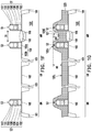
- the semiconductor device 10 includes the substrate 100 , the dummy gate structure DG, the logic gate structure LG, and the memory cells MC in the dummy region DR, the logic region LR, and a memory cell region MR respectively.
- Each of the memory cells includes adjacent two stack structures S 1 and S 2 , two select gates 126 , and an erase gate 124 .
- the two select gates 126 are located outside the two stack structures S 1 , and S 2 respectively.
- the erase gate 124 is located between adjacent two stack structures S 1 and S 2 .
- the second width W 2 is greater than the first width W 1 .
- the second width W 2 is greater than two times of the first width W 1 .
- the first width W 1 of one of the two select gates 126 is in a range from about 170 nm to about 210 nm, while the second width W 2 of the erase gate 124 is in a range from about 290 nm to about 360 nm, for example.
- the top surfaces of the select gates 126 are substantially flat. In some other embodiments, the top surfaces of the select gates 126 have bar-shaped surfaces in the section view or plane surfaces. In some other embodiments, a difference between a topmost top surface and a lowermost top surface of one of the select gates 126 is less than 10 nm. In other words, the top surface of one of the select gates 126 and the topmost top surface 124 U of the erase gate 124 are substantially coplanar, in some embodiments.
- the step height H 2 exists between a topmost top surface 124 U and a lowermost top surface 124 L of the erase gate 124 , so that the top surface of the erase gate 124 is a U-shaped surface in the section view.
- the step height H 2 ranges from 1 nm to 50 nm. In other words, in some embodiments, the step height H 2 between a topmost top surface 124 U and a lowermost top surface 124 L of the erase gate 124 is greater than the difference between the topmost top surface and the lowermost top surface of one of the select gates 126 .
- the silicide layer 142 formed over the top surface of the erase gate 124 also has the U-shaped surface.
- the silicide layers 142 formed over the top surfaces of the select gates 126 also have bar-shaped surfaces in the section view or plane surfaces.
- the select gates 126 are electrically connected to an interconnect (not shown) over the ILD layer 136 by the silicide layers 142 .
- the dummy gate structure DG is electrically floating. That is, the dummy gate structure DG is not electrically connected to any outside circuits.
- a method of manufacturing a semiconductor device includes following steps.
- the substrate includes a dummy region and a memory cell region.
- a plurality of first stack structures are formed over the substrate in the memory cell region.
- At least one second stack structure is formed over the substrate in the dummy region.
- a conductive layer is formed over the substrate to cover the first stack structures and the at least one second stack structure.
- a planarization process is performed on the conductive layer to expose top surfaces of the first stack structures and the at least one second stack structure.
- the conductive layer is patterned to form an erase gate between adjacent two first stack structures, and to form first and second select gates outside the adjacent two first stack structures.
- a semiconductor device includes a substrate, a plurality of memory cells, and at least one dummy gate structure.
- the substrate has a dummy region and a memory cell region.
- the memory cells are located over the substrate in the memory cell region.
- Each of the memory cells includes adjacent two stack structures, two select gates, and an erase gate on the substrate.
- the two select gates are located outside the two stack structures respectively.
- the erase gate is located between adjacent two stack structures.
- a step height exists between a topmost top surface and a lowermost top surface of the erase gate.
- the at least one dummy gate structure is located over the substrate in the dummy region.
- a method of manufacturing a semiconductor device having a memory includes following steps.
- a plurality of stack structures are formed over a substrate.
- Each of the stack structures includes a first dielectric layer, a first conductive layer, a second dielectric layer, a second conductive layer and a cap layer from bottom to top.
- Each of the stack structures further includes spacers overlying sidewalls of the first conductive layer, the second dielectric layer, the second conductive layer and the cap layer, and covering the first dielectric layer.
- a third conductive layer is conformally formed over the substrate to cover the stack structures.
- a planarization process is performed on the third conductive layer to expose top surfaces of the stack structures.
- the third conductive layer is patterned to form two select gates outside adjacent two stack structures and on the first dielectric layer, and to form an erase gate between the adjacent two stack structures after the planarization process is performed.
Landscapes
- Engineering & Computer Science (AREA)
- Manufacturing & Machinery (AREA)
- Microelectronics & Electronic Packaging (AREA)
- Condensed Matter Physics & Semiconductors (AREA)
- General Physics & Mathematics (AREA)
- Computer Hardware Design (AREA)
- Physics & Mathematics (AREA)
- Power Engineering (AREA)
- Chemical & Material Sciences (AREA)
- Semiconductor Memories (AREA)
- Crystallography & Structural Chemistry (AREA)
- Materials Engineering (AREA)
- Chemical Kinetics & Catalysis (AREA)
- General Chemical & Material Sciences (AREA)
- Non-Volatile Memory (AREA)
Abstract
Description
Claims (20)
Priority Applications (5)
| Application Number | Priority Date | Filing Date | Title |
|---|---|---|---|
| US16/180,026 US10825914B2 (en) | 2017-11-13 | 2018-11-05 | Manufacturing method of semiconductor device |
| TW107140101A TWI701810B (en) | 2017-11-13 | 2018-11-12 | Semiconductor device and manufacturing method thereof |
| CN201811343392.6A CN109786386B (en) | 2017-11-13 | 2018-11-13 | Semiconductor device and method for manufacturing the same |
| US17/068,769 US11411097B2 (en) | 2017-11-13 | 2020-10-12 | Semiconductor device |
| US17/848,378 US11764285B2 (en) | 2017-11-13 | 2022-06-23 | Method of manufacturing semiconductor device |
Applications Claiming Priority (2)
| Application Number | Priority Date | Filing Date | Title |
|---|---|---|---|
| US201762584918P | 2017-11-13 | 2017-11-13 | |
| US16/180,026 US10825914B2 (en) | 2017-11-13 | 2018-11-05 | Manufacturing method of semiconductor device |
Related Child Applications (1)
| Application Number | Title | Priority Date | Filing Date |
|---|---|---|---|
| US17/068,769 Division US11411097B2 (en) | 2017-11-13 | 2020-10-12 | Semiconductor device |
Publications (2)
| Publication Number | Publication Date |
|---|---|
| US20190148513A1 US20190148513A1 (en) | 2019-05-16 |
| US10825914B2 true US10825914B2 (en) | 2020-11-03 |
Family
ID=66433621
Family Applications (3)
| Application Number | Title | Priority Date | Filing Date |
|---|---|---|---|
| US16/180,026 Active US10825914B2 (en) | 2017-11-13 | 2018-11-05 | Manufacturing method of semiconductor device |
| US17/068,769 Active US11411097B2 (en) | 2017-11-13 | 2020-10-12 | Semiconductor device |
| US17/848,378 Active US11764285B2 (en) | 2017-11-13 | 2022-06-23 | Method of manufacturing semiconductor device |
Family Applications After (2)
| Application Number | Title | Priority Date | Filing Date |
|---|---|---|---|
| US17/068,769 Active US11411097B2 (en) | 2017-11-13 | 2020-10-12 | Semiconductor device |
| US17/848,378 Active US11764285B2 (en) | 2017-11-13 | 2022-06-23 | Method of manufacturing semiconductor device |
Country Status (3)
| Country | Link |
|---|---|
| US (3) | US10825914B2 (en) |
| CN (1) | CN109786386B (en) |
| TW (1) | TWI701810B (en) |
Families Citing this family (13)
| Publication number | Priority date | Publication date | Assignee | Title |
|---|---|---|---|---|
| US10535670B2 (en) * | 2016-02-25 | 2020-01-14 | Taiwan Semiconductor Manufacturing Co., Ltd. | Non-volatile memory having an erase gate formed between two floating gates with two word lines formed on other sides and a method for forming the same |
| US10825914B2 (en) * | 2017-11-13 | 2020-11-03 | Taiwan Semiconductor Manufacturing Company, Ltd. | Manufacturing method of semiconductor device |
| TWI702715B (en) * | 2019-07-24 | 2020-08-21 | 漢薩科技股份有限公司 | Semiconductor device and fabrication method thereof |
| CN110729296B (en) * | 2019-10-21 | 2022-03-22 | 长江存储科技有限责任公司 | Three-dimensional memory and method of forming the same |
| CN111079201B (en) * | 2019-12-09 | 2021-12-03 | 华中科技大学 | Safety NVM system and data recovery method after crash |
| US11183571B2 (en) | 2020-01-16 | 2021-11-23 | Taiwan Semiconductor Manufacturing Co., Ltd. | Memory device and manufacturing method thereof |
| US11362218B2 (en) * | 2020-06-23 | 2022-06-14 | Silicon Storage Technology, Inc. | Method of forming split gate memory cells with thinned side edge tunnel oxide |
| CN114823918B (en) | 2021-01-22 | 2025-12-23 | 联华电子股份有限公司 | Flash memory and its manufacturing method |
| KR102479666B1 (en) | 2021-05-07 | 2022-12-21 | 주식회사 키파운드리 | Semiconductor Device including Non-Volatile Memory Cell and Manufacturing Method Thereof |
| TWI891870B (en) | 2021-08-02 | 2025-08-01 | 聯華電子股份有限公司 | Semiconductor memory device and fabrication method thereof |
| CN114743976B (en) * | 2022-05-10 | 2025-09-23 | 杭州知存算力科技有限公司 | Semiconductor device and method for manufacturing the same |
| US20240304692A1 (en) * | 2023-03-10 | 2024-09-12 | Iotmemory Technology Inc. | Non-volatile memory device and method for manufacturing the same |
| US20250318111A1 (en) * | 2024-04-03 | 2025-10-09 | Nanya Technology Corporation | Semiconductor device and manufacturing method thereof |
Citations (5)
| Publication number | Priority date | Publication date | Assignee | Title |
|---|---|---|---|---|
| US20180145085A1 (en) * | 2016-11-18 | 2018-05-24 | Taiwan Semiconductor Manufacturing Company Ltd. | Logic-compatible memory cell manufacturing method and structure thereof |
| US20180151579A1 (en) * | 2016-11-29 | 2018-05-31 | Taiwan Semiconductor Manufacturing Co., Ltd. | Cell boundary structure for embedded memory |
| US20190067302A1 (en) * | 2017-08-30 | 2019-02-28 | Taiwan Semiconductor Manufacturing Co., Ltd. | High-k metal gate (hkmg) process for forming a memory cell with a large operation window |
| US20190393234A1 (en) * | 2018-06-26 | 2019-12-26 | Taiwan Semiconductor Manufacturing Co., Ltd. | Method to improve fill-in window for embedded memory |
| US20200058665A1 (en) * | 2018-08-15 | 2020-02-20 | Taiwan Semiconductor Manufacturing Co., Ltd. | Cell boundary structure for embedded memory |
Family Cites Families (24)
| Publication number | Priority date | Publication date | Assignee | Title |
|---|---|---|---|---|
| US5885856A (en) * | 1996-08-21 | 1999-03-23 | Motorola, Inc. | Integrated circuit having a dummy structure and method of making |
| TWI289344B (en) * | 2006-01-02 | 2007-11-01 | Powerchip Semiconductor Corp | Method of fabricating flash memory |
| CN100517723C (en) * | 2006-01-23 | 2009-07-22 | 株式会社东芝 | Nonvolatile semiconductor storage device |
| TW200826242A (en) * | 2006-12-12 | 2008-06-16 | Powerchip Semiconductor Corp | Manufacturing method of non-volatile memory |
| US9991285B2 (en) * | 2013-10-30 | 2018-06-05 | Taiwan Semiconductor Manufacturing Company, Ltd. | Mechanisms for forming FinFET device |
| US20150364549A1 (en) * | 2014-06-11 | 2015-12-17 | Mediatek Inc. | Semiconductor device with silicon carbide embedded dummy pattern |
| TWI612563B (en) * | 2014-07-07 | 2018-01-21 | United Microelectronics Corp. | Metal gate structure and manufacturing method thereof |
| US9559146B2 (en) * | 2014-12-23 | 2017-01-31 | Intel Corporation | Phase-change memory cell implant for dummy array leakage reduction |
| US20160190146A1 (en) * | 2014-12-29 | 2016-06-30 | GLOBAL FOUNDRIES Singapore Pte. Ltd. | Integrated circuits and methods for fabricating memory cells and integrated circuits |
| US9634019B1 (en) * | 2015-10-01 | 2017-04-25 | Silicon Storage Technology, Inc. | Non-volatile split gate memory cells with integrated high K metal gate, and method of making same |
| KR102514041B1 (en) * | 2015-12-09 | 2023-03-24 | 삼성전자주식회사 | Method for fabricating semiconductor device |
| US10163719B2 (en) * | 2015-12-15 | 2018-12-25 | Taiwan Semiconductor Manufacturing Company, Ltd. | Method of forming self-alignment contact |
| US10535670B2 (en) * | 2016-02-25 | 2020-01-14 | Taiwan Semiconductor Manufacturing Co., Ltd. | Non-volatile memory having an erase gate formed between two floating gates with two word lines formed on other sides and a method for forming the same |
| US10510544B2 (en) * | 2016-11-29 | 2019-12-17 | Taiwan Semiconductor Manufacturing Co., Ltd. | Non-volatile memory semiconductor device and manufacturing method thereof |
| US20180175209A1 (en) * | 2016-12-20 | 2018-06-21 | Globalfoundries Inc. | Semiconductor structure including one or more nonvolatile memory cells and method for the formation thereof |
| US10720516B2 (en) * | 2017-06-30 | 2020-07-21 | Taiwan Semiconductor Manufacturing Company, Ltd. | Gate stack structure and method for forming the same |
| US10515977B2 (en) * | 2017-07-26 | 2019-12-24 | Taiwan Semiconductor Manufacturing Co., Ltd. | Boundary design to reduce memory array edge CMP dishing effect |
| US10535574B2 (en) * | 2017-09-20 | 2020-01-14 | Taiwan Semiconductor Manufacturing Co., Ltd. | Cell-like floating-gate test structure |
| US10825914B2 (en) * | 2017-11-13 | 2020-11-03 | Taiwan Semiconductor Manufacturing Company, Ltd. | Manufacturing method of semiconductor device |
| US10381360B1 (en) * | 2018-03-22 | 2019-08-13 | Globalfoundries Singapore Pte. Ltd. | Control gate dummy for word line uniformity and method for producing the same |
| US11189727B2 (en) * | 2019-08-23 | 2021-11-30 | Taiwan Semiconductor Manufacturing Company, Ltd. | FinFET contacts and method forming same |
| US11380769B2 (en) * | 2019-10-01 | 2022-07-05 | Taiwan Semiconductor Manufacturing Company, Ltd. | Select gate spacer formation to facilitate embedding of split gate flash memory |
| US11211469B2 (en) * | 2020-05-28 | 2021-12-28 | Taiwan Semiconductor Manufacturing Company Limited | Third generation flash memory structure with self-aligned contact and methods for forming the same |
| US11527630B2 (en) * | 2020-06-24 | 2022-12-13 | Taiwan Semiconductor Manufacturing Co., Ltd. | Semiconductor device and method for fabricating the same |
-
2018
- 2018-11-05 US US16/180,026 patent/US10825914B2/en active Active
- 2018-11-12 TW TW107140101A patent/TWI701810B/en active
- 2018-11-13 CN CN201811343392.6A patent/CN109786386B/en active Active
-
2020
- 2020-10-12 US US17/068,769 patent/US11411097B2/en active Active
-
2022
- 2022-06-23 US US17/848,378 patent/US11764285B2/en active Active
Patent Citations (5)
| Publication number | Priority date | Publication date | Assignee | Title |
|---|---|---|---|---|
| US20180145085A1 (en) * | 2016-11-18 | 2018-05-24 | Taiwan Semiconductor Manufacturing Company Ltd. | Logic-compatible memory cell manufacturing method and structure thereof |
| US20180151579A1 (en) * | 2016-11-29 | 2018-05-31 | Taiwan Semiconductor Manufacturing Co., Ltd. | Cell boundary structure for embedded memory |
| US20190067302A1 (en) * | 2017-08-30 | 2019-02-28 | Taiwan Semiconductor Manufacturing Co., Ltd. | High-k metal gate (hkmg) process for forming a memory cell with a large operation window |
| US20190393234A1 (en) * | 2018-06-26 | 2019-12-26 | Taiwan Semiconductor Manufacturing Co., Ltd. | Method to improve fill-in window for embedded memory |
| US20200058665A1 (en) * | 2018-08-15 | 2020-02-20 | Taiwan Semiconductor Manufacturing Co., Ltd. | Cell boundary structure for embedded memory |
Also Published As
| Publication number | Publication date |
|---|---|
| US20190148513A1 (en) | 2019-05-16 |
| US11764285B2 (en) | 2023-09-19 |
| TWI701810B (en) | 2020-08-11 |
| CN109786386A (en) | 2019-05-21 |
| US20210043752A1 (en) | 2021-02-11 |
| TW201937703A (en) | 2019-09-16 |
| US11411097B2 (en) | 2022-08-09 |
| CN109786386B (en) | 2022-11-11 |
| US20220320315A1 (en) | 2022-10-06 |
Similar Documents
| Publication | Publication Date | Title |
|---|---|---|
| US11764285B2 (en) | Method of manufacturing semiconductor device | |
| US11527540B2 (en) | Implantations for forming source/drain regions of different transistors | |
| US11417670B2 (en) | Structure and method for single gate non-volatile memory device | |
| US11594620B2 (en) | Semiconductor device and manufacturing method thereof | |
| JP6249888B2 (en) | Semiconductor device | |
| US11758721B2 (en) | Semiconductor device and manufacturing method thereof | |
| US11778812B2 (en) | Method for forming a semiconductor device with conductive cap layer over conductive plug | |
| TWI701729B (en) | Pad structure and manufacturing method thereof in semiconductor device | |
| US20120025295A1 (en) | Semiconductor memory device and method of manufacturing the same | |
| US20070243671A1 (en) | Butted source contact and well strap | |
| JP4256742B2 (en) | Integrated metal insulator metal capacitor and method for forming metal gate transistor | |
| US7285377B2 (en) | Fabrication method for a damascene bit line contact plug | |
| US20050026373A1 (en) | Method for fabricating transistors of different conduction types and having different packing densities in a semiconductor substrate | |
| CN101207079A (en) | Integrated circuit, semiconductor device and manufacturing method | |
| US7172939B1 (en) | Method and structure for fabricating non volatile memory arrays | |
| US6967161B2 (en) | Method and resulting structure for fabricating DRAM cell structure using oxide line spacer | |
| JP2014187132A (en) | Semiconductor device | |
| US12245423B2 (en) | Semiconductor device with conductive cap layer over conductive plug and method for preparinging the same |
Legal Events
| Date | Code | Title | Description |
|---|---|---|---|
| FEPP | Fee payment procedure |
Free format text: ENTITY STATUS SET TO UNDISCOUNTED (ORIGINAL EVENT CODE: BIG.); ENTITY STATUS OF PATENT OWNER: LARGE ENTITY |
|
| AS | Assignment |
Owner name: TAIWAN SEMICONDUCTOR MANUFACTURING CO., LTD., TAIW Free format text: ASSIGNMENT OF ASSIGNORS INTEREST;ASSIGNORS:LIN, YI-CHUAN;CHUANG, CHIANG-MING;WU, SHANG-YEN;SIGNING DATES FROM 20181129 TO 20181204;REEL/FRAME:047812/0117 Owner name: TAIWAN SEMICONDUCTOR MANUFACTURING CO., LTD., TAIWAN Free format text: ASSIGNMENT OF ASSIGNORS INTEREST;ASSIGNORS:LIN, YI-CHUAN;CHUANG, CHIANG-MING;WU, SHANG-YEN;SIGNING DATES FROM 20181129 TO 20181204;REEL/FRAME:047812/0117 |
|
| STPP | Information on status: patent application and granting procedure in general |
Free format text: DOCKETED NEW CASE - READY FOR EXAMINATION |
|
| STPP | Information on status: patent application and granting procedure in general |
Free format text: NON FINAL ACTION MAILED |
|
| STPP | Information on status: patent application and granting procedure in general |
Free format text: RESPONSE TO NON-FINAL OFFICE ACTION ENTERED AND FORWARDED TO EXAMINER |
|
| STPP | Information on status: patent application and granting procedure in general |
Free format text: EX PARTE QUAYLE ACTION MAILED |
|
| STPP | Information on status: patent application and granting procedure in general |
Free format text: NOTICE OF ALLOWANCE MAILED -- APPLICATION RECEIVED IN OFFICE OF PUBLICATIONS |
|
| STPP | Information on status: patent application and granting procedure in general |
Free format text: PUBLICATIONS -- ISSUE FEE PAYMENT VERIFIED |
|
| STCF | Information on status: patent grant |
Free format text: PATENTED CASE |
|
| MAFP | Maintenance fee payment |
Free format text: PAYMENT OF MAINTENANCE FEE, 4TH YEAR, LARGE ENTITY (ORIGINAL EVENT CODE: M1551); ENTITY STATUS OF PATENT OWNER: LARGE ENTITY Year of fee payment: 4 |