US10818792B2 - Nanosheet field-effect transistors formed with sacrificial spacers - Google Patents
Nanosheet field-effect transistors formed with sacrificial spacers Download PDFInfo
- Publication number
- US10818792B2 US10818792B2 US16/106,291 US201816106291A US10818792B2 US 10818792 B2 US10818792 B2 US 10818792B2 US 201816106291 A US201816106291 A US 201816106291A US 10818792 B2 US10818792 B2 US 10818792B2
- Authority
- US
- United States
- Prior art keywords
- dielectric material
- low
- layer
- channel layers
- nanosheet channel
- Prior art date
- Legal status (The legal status is an assumption and is not a legal conclusion. Google has not performed a legal analysis and makes no representation as to the accuracy of the status listed.)
- Active, expires
Links
Images


Classifications
-
- H—ELECTRICITY
- H10—SEMICONDUCTOR DEVICES; ELECTRIC SOLID-STATE DEVICES NOT OTHERWISE PROVIDED FOR
- H10D—INORGANIC ELECTRIC SEMICONDUCTOR DEVICES
- H10D30/00—Field-effect transistors [FET]
- H10D30/60—Insulated-gate field-effect transistors [IGFET]
- H10D30/62—Fin field-effect transistors [FinFET]
-
- H01L29/785—
-
- B—PERFORMING OPERATIONS; TRANSPORTING
- B82—NANOTECHNOLOGY
- B82Y—SPECIFIC USES OR APPLICATIONS OF NANOSTRUCTURES; MEASUREMENT OR ANALYSIS OF NANOSTRUCTURES; MANUFACTURE OR TREATMENT OF NANOSTRUCTURES
- B82Y10/00—Nanotechnology for information processing, storage or transmission, e.g. quantum computing or single electron logic
-
- H01L21/76837—
-
- H01L21/823412—
-
- H01L21/823431—
-
- H01L21/823468—
-
- H01L29/0673—
-
- H01L29/0847—
-
- H01L29/66545—
-
- H01L29/6656—
-
- H01L29/6681—
-
- H—ELECTRICITY
- H10—SEMICONDUCTOR DEVICES; ELECTRIC SOLID-STATE DEVICES NOT OTHERWISE PROVIDED FOR
- H10D—INORGANIC ELECTRIC SEMICONDUCTOR DEVICES
- H10D30/00—Field-effect transistors [FET]
- H10D30/01—Manufacture or treatment
- H10D30/014—Manufacture or treatment of FETs having zero-dimensional [0D] or one-dimensional [1D] channels, e.g. quantum wire FETs, single-electron transistors [SET] or Coulomb blockade transistors
-
- H—ELECTRICITY
- H10—SEMICONDUCTOR DEVICES; ELECTRIC SOLID-STATE DEVICES NOT OTHERWISE PROVIDED FOR
- H10D—INORGANIC ELECTRIC SEMICONDUCTOR DEVICES
- H10D30/00—Field-effect transistors [FET]
- H10D30/01—Manufacture or treatment
- H10D30/021—Manufacture or treatment of FETs having insulated gates [IGFET]
- H10D30/024—Manufacture or treatment of FETs having insulated gates [IGFET] of fin field-effect transistors [FinFET]
- H10D30/0243—Manufacture or treatment of FETs having insulated gates [IGFET] of fin field-effect transistors [FinFET] using dummy structures having essentially the same shapes as the semiconductor bodies, e.g. to provide stability
-
- H—ELECTRICITY
- H10—SEMICONDUCTOR DEVICES; ELECTRIC SOLID-STATE DEVICES NOT OTHERWISE PROVIDED FOR
- H10D—INORGANIC ELECTRIC SEMICONDUCTOR DEVICES
- H10D30/00—Field-effect transistors [FET]
- H10D30/40—FETs having zero-dimensional [0D], one-dimensional [1D] or two-dimensional [2D] charge carrier gas channels
- H10D30/43—FETs having zero-dimensional [0D], one-dimensional [1D] or two-dimensional [2D] charge carrier gas channels having one-dimensional [1D] charge carrier gas channels, e.g. quantum wire FETs or transistors having 1D quantum-confined channels
-
- H—ELECTRICITY
- H10—SEMICONDUCTOR DEVICES; ELECTRIC SOLID-STATE DEVICES NOT OTHERWISE PROVIDED FOR
- H10D—INORGANIC ELECTRIC SEMICONDUCTOR DEVICES
- H10D30/00—Field-effect transistors [FET]
- H10D30/60—Insulated-gate field-effect transistors [IGFET]
- H10D30/67—Thin-film transistors [TFT]
- H10D30/6729—Thin-film transistors [TFT] characterised by the electrodes
- H10D30/673—Thin-film transistors [TFT] characterised by the electrodes characterised by the shapes, relative sizes or dispositions of the gate electrodes
- H10D30/6735—Thin-film transistors [TFT] characterised by the electrodes characterised by the shapes, relative sizes or dispositions of the gate electrodes having gates fully surrounding the channels, e.g. gate-all-around
-
- H—ELECTRICITY
- H10—SEMICONDUCTOR DEVICES; ELECTRIC SOLID-STATE DEVICES NOT OTHERWISE PROVIDED FOR
- H10D—INORGANIC ELECTRIC SEMICONDUCTOR DEVICES
- H10D30/00—Field-effect transistors [FET]
- H10D30/60—Insulated-gate field-effect transistors [IGFET]
- H10D30/67—Thin-film transistors [TFT]
- H10D30/6757—Thin-film transistors [TFT] characterised by the structure of the channel, e.g. transverse or longitudinal shape or doping profile
-
- H—ELECTRICITY
- H10—SEMICONDUCTOR DEVICES; ELECTRIC SOLID-STATE DEVICES NOT OTHERWISE PROVIDED FOR
- H10D—INORGANIC ELECTRIC SEMICONDUCTOR DEVICES
- H10D62/00—Semiconductor bodies, or regions thereof, of devices having potential barriers
- H10D62/10—Shapes, relative sizes or dispositions of the regions of the semiconductor bodies; Shapes of the semiconductor bodies
- H10D62/113—Isolations within a component, i.e. internal isolations
- H10D62/115—Dielectric isolations, e.g. air gaps
- H10D62/116—Dielectric isolations, e.g. air gaps adjoining the input or output regions of field-effect devices, e.g. adjoining source or drain regions
-
- H—ELECTRICITY
- H10—SEMICONDUCTOR DEVICES; ELECTRIC SOLID-STATE DEVICES NOT OTHERWISE PROVIDED FOR
- H10D—INORGANIC ELECTRIC SEMICONDUCTOR DEVICES
- H10D62/00—Semiconductor bodies, or regions thereof, of devices having potential barriers
- H10D62/10—Shapes, relative sizes or dispositions of the regions of the semiconductor bodies; Shapes of the semiconductor bodies
- H10D62/117—Shapes of semiconductor bodies
- H10D62/118—Nanostructure semiconductor bodies
- H10D62/119—Nanowire, nanosheet or nanotube semiconductor bodies
- H10D62/121—Nanowire, nanosheet or nanotube semiconductor bodies oriented parallel to substrates
-
- H—ELECTRICITY
- H10—SEMICONDUCTOR DEVICES; ELECTRIC SOLID-STATE DEVICES NOT OTHERWISE PROVIDED FOR
- H10D—INORGANIC ELECTRIC SEMICONDUCTOR DEVICES
- H10D62/00—Semiconductor bodies, or regions thereof, of devices having potential barriers
- H10D62/10—Shapes, relative sizes or dispositions of the regions of the semiconductor bodies; Shapes of the semiconductor bodies
- H10D62/13—Semiconductor regions connected to electrodes carrying current to be rectified, amplified or switched, e.g. source or drain regions
- H10D62/149—Source or drain regions of field-effect devices
- H10D62/151—Source or drain regions of field-effect devices of IGFETs
-
- H—ELECTRICITY
- H10—SEMICONDUCTOR DEVICES; ELECTRIC SOLID-STATE DEVICES NOT OTHERWISE PROVIDED FOR
- H10D—INORGANIC ELECTRIC SEMICONDUCTOR DEVICES
- H10D64/00—Electrodes of devices having potential barriers
- H10D64/01—Manufacture or treatment
- H10D64/017—Manufacture or treatment using dummy gates in processes wherein at least parts of the final gates are self-aligned to the dummy gates, i.e. replacement gate processes
-
- H—ELECTRICITY
- H10—SEMICONDUCTOR DEVICES; ELECTRIC SOLID-STATE DEVICES NOT OTHERWISE PROVIDED FOR
- H10D—INORGANIC ELECTRIC SEMICONDUCTOR DEVICES
- H10D64/00—Electrodes of devices having potential barriers
- H10D64/01—Manufacture or treatment
- H10D64/021—Manufacture or treatment using multiple gate spacer layers, e.g. bilayered sidewall spacers
-
- H—ELECTRICITY
- H10—SEMICONDUCTOR DEVICES; ELECTRIC SOLID-STATE DEVICES NOT OTHERWISE PROVIDED FOR
- H10D—INORGANIC ELECTRIC SEMICONDUCTOR DEVICES
- H10D84/00—Integrated devices formed in or on semiconductor substrates that comprise only semiconducting layers, e.g. on Si wafers or on GaAs-on-Si wafers
- H10D84/01—Manufacture or treatment
- H10D84/0123—Integrating together multiple components covered by H10D12/00 or H10D30/00, e.g. integrating multiple IGBTs
- H10D84/0126—Integrating together multiple components covered by H10D12/00 or H10D30/00, e.g. integrating multiple IGBTs the components including insulated gates, e.g. IGFETs
- H10D84/0128—Manufacturing their channels
-
- H—ELECTRICITY
- H10—SEMICONDUCTOR DEVICES; ELECTRIC SOLID-STATE DEVICES NOT OTHERWISE PROVIDED FOR
- H10D—INORGANIC ELECTRIC SEMICONDUCTOR DEVICES
- H10D84/00—Integrated devices formed in or on semiconductor substrates that comprise only semiconducting layers, e.g. on Si wafers or on GaAs-on-Si wafers
- H10D84/01—Manufacture or treatment
- H10D84/0123—Integrating together multiple components covered by H10D12/00 or H10D30/00, e.g. integrating multiple IGBTs
- H10D84/0126—Integrating together multiple components covered by H10D12/00 or H10D30/00, e.g. integrating multiple IGBTs the components including insulated gates, e.g. IGFETs
- H10D84/0147—Manufacturing their gate sidewall spacers
-
- H—ELECTRICITY
- H10—SEMICONDUCTOR DEVICES; ELECTRIC SOLID-STATE DEVICES NOT OTHERWISE PROVIDED FOR
- H10D—INORGANIC ELECTRIC SEMICONDUCTOR DEVICES
- H10D84/00—Integrated devices formed in or on semiconductor substrates that comprise only semiconducting layers, e.g. on Si wafers or on GaAs-on-Si wafers
- H10D84/01—Manufacture or treatment
- H10D84/0123—Integrating together multiple components covered by H10D12/00 or H10D30/00, e.g. integrating multiple IGBTs
- H10D84/0126—Integrating together multiple components covered by H10D12/00 or H10D30/00, e.g. integrating multiple IGBTs the components including insulated gates, e.g. IGFETs
- H10D84/0158—Integrating together multiple components covered by H10D12/00 or H10D30/00, e.g. integrating multiple IGBTs the components including insulated gates, e.g. IGFETs the components including FinFETs
-
- H—ELECTRICITY
- H10—SEMICONDUCTOR DEVICES; ELECTRIC SOLID-STATE DEVICES NOT OTHERWISE PROVIDED FOR
- H10D—INORGANIC ELECTRIC SEMICONDUCTOR DEVICES
- H10D84/00—Integrated devices formed in or on semiconductor substrates that comprise only semiconducting layers, e.g. on Si wafers or on GaAs-on-Si wafers
- H10D84/01—Manufacture or treatment
- H10D84/02—Manufacture or treatment characterised by using material-based technologies
- H10D84/03—Manufacture or treatment characterised by using material-based technologies using Group IV technology, e.g. silicon technology or silicon-carbide [SiC] technology
- H10D84/038—Manufacture or treatment characterised by using material-based technologies using Group IV technology, e.g. silicon technology or silicon-carbide [SiC] technology using silicon technology, e.g. SiGe
-
- H—ELECTRICITY
- H10—SEMICONDUCTOR DEVICES; ELECTRIC SOLID-STATE DEVICES NOT OTHERWISE PROVIDED FOR
- H10D—INORGANIC ELECTRIC SEMICONDUCTOR DEVICES
- H10D84/00—Integrated devices formed in or on semiconductor substrates that comprise only semiconducting layers, e.g. on Si wafers or on GaAs-on-Si wafers
- H10D84/80—Integrated devices formed in or on semiconductor substrates that comprise only semiconducting layers, e.g. on Si wafers or on GaAs-on-Si wafers characterised by the integration of at least one component covered by groups H10D12/00 or H10D30/00, e.g. integration of IGFETs
- H10D84/82—Integrated devices formed in or on semiconductor substrates that comprise only semiconducting layers, e.g. on Si wafers or on GaAs-on-Si wafers characterised by the integration of at least one component covered by groups H10D12/00 or H10D30/00, e.g. integration of IGFETs of only field-effect components
- H10D84/83—Integrated devices formed in or on semiconductor substrates that comprise only semiconducting layers, e.g. on Si wafers or on GaAs-on-Si wafers characterised by the integration of at least one component covered by groups H10D12/00 or H10D30/00, e.g. integration of IGFETs of only field-effect components of only insulated-gate FETs [IGFET]
-
- H—ELECTRICITY
- H10—SEMICONDUCTOR DEVICES; ELECTRIC SOLID-STATE DEVICES NOT OTHERWISE PROVIDED FOR
- H10W—GENERIC PACKAGES, INTERCONNECTIONS, CONNECTORS OR OTHER CONSTRUCTIONAL DETAILS OF DEVICES COVERED BY CLASS H10
- H10W20/00—Interconnections in chips, wafers or substrates
- H10W20/01—Manufacture or treatment
- H10W20/071—Manufacture or treatment of dielectric parts thereof
- H10W20/098—Manufacture or treatment of dielectric parts thereof by filling between adjacent conductive parts
Definitions
- Nanosheet field-effect transistors have been developed as a type of non-planar field-effect transistor that may permit additional increases in packing density in an integrated circuit.
- a nanosheet field-effect transistor includes multiple nanosheet channel layers that are arranged in a layer stack and source/drain regions connected with the ends of the nanosheet channel layers.
- the nanosheet channel layers are initially arranged in the layer stack with sacrificial layers containing a material (e.g., silicon-germanium) that alternate with the nanosheet channel layers and that can be etched selectively to the material (e.g., silicon) constituting the nanosheet channel layers.
- the sacrificial layers are etched and removed in order to release the nanosheet channel layers and to provide spaces for the formation of the sections of a gate stack. Sections of the gate stack may surround all sides of the individual nanosheet channel layers in a gate-all-around arrangement.
- the sacrificial layers are recessed to form divots or indents in the layer stack.
- the indents are filled with a dielectric material to define inner spacers that eventually isolate the gate stack from the source/drain regions.
- a conformal layer is deposited that pinches off inside the indents to form the inner spacers.
- a dielectric etch back is performed to remove excess dielectric material of the conformal layer from the ends of the nanosheet channel layers, which is needed for the subsequent epitaxial growth of the source/drain regions.
- the deposited conformal layer may pinch off and occlude the narrowed space between the gate stack on adjacent layer stacks of nanosheet channel layers. If this space is occluded, the inners spacers cannot be reliably formed.
- a method for forming a field-effect transistor.
- the method includes epitaxially growing a layer stack including a plurality of nanosheet channel layers and a plurality of sacrificial layers arranged to alternate with the plurality of nanosheet channel layers.
- First and second gate structures are formed that extend across the layer stack and that are separated by a first gap.
- the method further includes forming a first sidewall spacer and a second sidewall spacer over the layer stack and within the first gap respectively adjacent to the first gate structure and the second gate structure.
- the layer stack is etched to form a first body feature and a second body feature separated from the first body feature by a second gap.
- the method further includes recessing the plurality of sacrificial layers relative to the plurality of nanosheet channel layers to define a plurality of indents in the first body feature and the second body feature. After recessing the plurality of sacrificial layers, the first sidewall spacer and the second sidewall spacer are removed. The method further includes, after removing the first sidewall spacer and the second sidewall spacer, depositing a conformal layer in the second gap that fills the plurality of indents to define a plurality of inner spacers.
- a method for forming a field-effect transistor.
- the method includes forming a layer stack including a plurality of nanosheet channel layers and a plurality of sacrificial layers arranged to alternate with the nanosheet channel layers, forming a gate structure extending across the layer stack, and forming a sidewall spacer adjacent to the gate structure.
- the layer stack is etched to form a body feature.
- the method further includes recessing the sacrificial layers relative to the nanosheet channel layers to define a plurality of indents in the body feature.
- the first sidewall spacer is removed, and a conformal layer is deposited over the body feature and the gate structure that fills the indents to define a plurality of inner spacers.
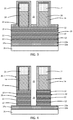
- FIG. 1 is a top view of a device structure at an initial fabrication stage of the processing method in accordance with embodiments of the invention.
- FIGS. 3-13 are cross-sectional views of the device structure at successive fabrication stages of the processing method subsequent to FIG. 2 .
- nanosheet channel layers 10 , sacrificial layers 12 , and a sacrificial layer 14 are arranged in patterned layer stack 15 on a substrate 16 .
- the substrate 16 may be composed of a semiconductor material, such as single-crystal silicon. Shallow trench isolation regions 13 may be arranged about the patterned layer stack 15 .
- the nanosheet channel layers 10 and sacrificial layers 12 , 14 may be formed on the substrate 16 by an epitaxial growth process during which the composition is alternated through variation of the reactants supplied to the deposition tool.
- the nanosheet channel layers 10 and sacrificial layers 12 , 14 may be patterned after growth using lithography and etching processes to form the layer stack 15 .
- the number of nanosheet channel layers 10 and sacrificial layers 12 in the layer stack 15 may differ from the number in the depicted representative embodiment and, in particular, may be greater than the number in the representative embodiment through the addition of pairs of nanosheet channel layers 10 and sacrificial layers 12 to the layer stack 15 .
- the nanosheet channel layers 10 are composed of a semiconductor material
- the sacrificial layers 12 are composed of a semiconductor material with a composition that is selected to be removed selective to the semiconductor material of the nanosheet channel layers 10
- the sacrificial layer 14 is composed of a semiconductor material with a composition that is selected to be removed selective to the semiconductor materials of both the nanosheet channel layers 10 and sacrificial layers 12 .
- the term “selective” in reference to a material removal process denotes that, with an appropriate etchant choice, the material removal rate (i.e., etch rate) for the targeted material is greater than the removal rate for at least another material exposed to the material removal process.
- the semiconductor material constituting the nanosheet channel layers 10 may be silicon (Si)
- the semiconductor material constituting the sacrificial layers 12 may be silicon-germanium (SiGe) that etches at a higher rate than silicon due to the germanium content
- the semiconductor material constituting the sacrificial layer 14 may be silicon-germanium (SiGe) that etches at a higher rate than the sacrificial layers 12 due to a higher germanium content.
- the germanium content of the sacrificial layers 12 may range from fifteen atomic percent (15 at. %) to thirty-five atomic percent (35 at. %)
- the germanium content of the sacrificial layer 14 may range from fifty atomic percent (50 at. %) to seventy-five atomic percent (75 at. %).
- Sacrificial gate structures 18 , 20 are formed that overlap with and wrap around the patterned layer stack 15 .
- the term “sacrificial gate structure” as used herein refers to a placeholder structure for a gate structure to be subsequently formed.
- the sacrificial gate structures 18 , 20 have a spaced-apart arrangement along the length of the layer stack 15 and are aligned transverse to the layer stack 15 .
- the sacrificial gate structures 18 , 20 are spaced apart by a gap 23 .
- the sacrificial gate structures 18 , 20 may include a thin layer containing, for example, silicon dioxide arranged adjacent to the layer stack 15 and a thick layer containing, for example, amorphous silicon over the thin layer.
- the sacrificial gate structures 18 , 20 are patterned from these constituent layers with reactive ion etching (RIE) using a hardmask.
- RIE reactive ion etching
- the sacrificial gate structures 18 , 20 may be cut along their lengths to define the locations of individual field-effect transistors and/or the sacrificial gate structures 18 , 20 may overlap with additional layer stacks similar to layer stack 15 .
- the sacrificial gate structures 18 , 20 are covered by a hardmask cap 21 arranged on their respective top surfaces.
- the hardmask cap 21 may include one or more dielectric materials, such as a layered combination of silicon dioxide over silicon nitride, and may be a remnant of the hardmask from the lithography and etching processes used to form the sacrificial gate structures 18 , 20 .
- the sacrificial layer 14 is removed by an etching process selective to the nanosheet channel layers 10 and the sacrificial layers 12 .
- a conformal dielectric liner 22 and a conformal dielectric layer 24 are sequentially formed on the sacrificial gate structures 18 , 20 and their hardmask caps 21 , as well as on surfaces of the uppermost sacrificial layer 12 between the sacrificial gate structures 18 , 20 .
- the dielectric liner 22 may be composed of silicon dioxide (SiO 2 ) deposited by atomic layer deposition (ALD), and the dielectric layer 24 may be composed of silicon-boron-carbon nitride (SiBCN) deposited by atomic layer deposition.
- ALD atomic layer deposition
- SiBCN silicon-boron-carbon nitride
- the dielectric material of the dielectric liner 22 also forms inside the cavity generated by the removal of the sacrificial layer 14 on the sacrificial layer 12 as a dielectric layer 22 a and on the substrate 16 as a dielectric layer 22 b .
- the dielectric material of the dielectric layer 25 also forms as a dielectric layer 24 a that fills the remaining space inside the cavity between the dielectric layers 22 a , 22 b.
- bilayer sidewall spacers 26 are formed at the sidewalls of the sacrificial gate structures 18 , 20 by etching the dielectric liner 22 and dielectric layer 24 with a directional etching process, such as reactive ion etching.
- the dielectric liner 22 provides an L-shaped component of the bilayer sidewall spacers 26
- the dielectric layer 24 provides the outermost component of the bilayer sidewall spacers 26 .
- the gap 23 between the sacrificial gate structures 18 , 20 is narrowed by the formation of the bilayer sidewall spacers 26 .
- the nanosheet channel layers 10 and sacrificial layers 12 are patterned to form body features 28 , 30 that each include one of the layer stacks 15 of patterned nanosheet channel layers 10 and sacrificial layers 12 .
- the body features 28 , 30 may be formed by a self-aligned etching process in which the respective sacrificial gate structures 18 , 20 and bilayer sidewall spacers 26 effectively operate as an etch mask.
- the self-aligned etching process which may be a reactive ion etching process, may utilize one or more etch chemistries to etch the nanosheet channel layers 10 and sacrificial layers 12 , and may stop on the dielectric layer 22 a .
- the body features 28 , 30 are separated from each other by a gap 29 after the patterning is completed. Due to the self-alignment, the gap 29 is equal or substantially equal to the gap 23 .
- the sacrificial layers 12 are laterally recessed relative to the nanosheet channel layers 10 with a dry or wet isotropic etching process that etches the semiconductor material constituting the sacrificial layers 12 selective to the semiconductor material constituting the nanosheet channel layers 10 .
- the lateral recessing of the sacrificial layers 12 generates indents 32 in the sidewalls of the body features 28 , 30 because the nanosheet channel layers 10 are not laterally recessed due to the etch selectivity of the isotropic etching process.
- the sacrificial layers 12 may be laterally recessed using a mixture of water (H 2 O), hydrogen peroxide (H 2 O 2 ), and ammonium hydroxide (NH 4 OH) (i.e., a wet SC1 clean).
- H 2 O water
- H 2 O 2 hydrogen peroxide
- NH 4 OH ammonium hydroxide
- the bilayer sidewall spacers 26 are removed with one or more etching processes to expose the sidewalls of the sacrificial gate structures 18 , 20 .
- the dielectric layer 22 a masks and protects underlying portions of the dielectric layer 24 a during the etching process removing the dielectric layer 24 of the bilayer sidewall spacers 26 .
- Portions of the dielectric layer 22 a exposed by the removal of dielectric layer 24 are subsequently removed by the etching process removing the dielectric liner 22 of the bilayer sidewall spacers 26 .
- the removal of the bilayer sidewall spacers 26 which are sacrificial, contrasts with a conventional process flow in which inner spacers are formed in the indents 32 with sidewall spacers in place adjacent to the sacrificial gate structures 18 , 20 .
- the removal of the bilayer sidewall spacers 26 increased the width of the gap 29 between the sacrificial gate structures 18 , 20 .
- a conformal layer 34 composed of a low-k dielectric material, such as carbon-doped silicon oxide (SiCO), is deposited by atomic layer deposition and fills the gap 29 between the body features 28 , 30 .
- a low-k dielectric material is characterized by a relative permittivity or dielectric constant that is less than the dielectric constant of silicon dioxide, which is about 3.9.
- the conformal layer 34 fills the indents 32 in the sidewalls of the body features 28 , 30 by pinch-off.
- the conformal layer 34 also coats the sacrificial gate structures 18 , 20 and their hardmask caps 21 .
- the prior removal of the bilayer sidewall spacers 26 effectively widens the gap 23 between the sacrificial gate structures 18 , 20 to promote improved filling of the gap 29 between the body features 28 , 30 and to prevent pinch-off inside the gap 23 during deposition of the conformal layer 34 .
- An etch mask 36 is applied and recessed with an etching process.
- the etch mask 36 may include material from an organic planarization layer (OPL) that is applied as a spin-on hardmask.
- OPL organic planarization layer
- the recessed etch mask 36 has a height that is a fraction of the height of the sacrificial gate structures 18 , 20 .
- an etching process is used to chamfer the conformal layer 34 to the height of the recessed etch mask 36 .
- the etching process may be performed by wet chemical etching or dry reactive ion etching.
- the etch mask 36 may be removed by, for example, ashing using an oxygen-based plasma.
- a conformal layer 38 composed of a low-k dielectric material, such as silicon-boron-carbon nitride (SiBCN), is deposited by atomic layer deposition.
- the conformal layer 38 coats the portions of the sacrificial gate structures 18 , 20 and their hardmask caps 21 exposed by the chamfering of the conformal layer 34 , and covers the conformal layer 34 residing in the gap 29 between the body features 28 , 30 .
- the dielectric material of conformal layer 38 is chosen to have etch selectivity relative to the dielectric material of conformal layer 34 .
- upper sidewall spacers 40 are formed at the sidewalls of the sacrificial gate structures 18 , 20 by etching the conformal layer 38 with a directional etching process, such as an anisotropic reactive ion etching process.
- the etching process removes the dielectric material of the conformal layer 38 selective to the dielectric material of the conformal layer 34 .
- lower sidewall spacers 42 are formed at the sidewalls of the sacrificial gate structures 18 , 20 by etching the conformal layer 34 with a directional etching process, such as an anisotropic reactive ion etching process.
- the etching process removes the dielectric material of the conformal layer 34 selective to the dielectric material of the conformal layer 38 , and the upper sidewall spacers 40 effectively provide an etch mask for self-aligned formation of the lower sidewall spacers 42 .
- the upper sidewall spacers 40 are arranged over the lower sidewall spacers 42 adjacent to the sidewalls of the sacrificial gate structures 18 , 20 , and the upper sidewall spacers 40 are stacked over (i.e., placed on top of) the lower sidewall spacers 42 . Due to etch selectivity between their dielectric materials, the upper sidewall spacers 40 are not pulled down to a significant extent by the etching process forming the lower sidewall spacers 42 . In addition, the upper sidewall spacers 40 and lower sidewall spacers 42 are formed without the necessity of a wet chemical etch as is conventional.
- the etching process also forms inner spacers 44 in the indents in the sidewalls of the body features 28 , 30 .
- the formation of the inner spacers 44 occurs later than in conventional process flows, and the inner spacers 44 are composed of a low-k dielectric material instead of silicon nitride or silicon oxide.
- source/drain regions 46 are formed adjacent to the side surfaces of each of the body features 28 , 30 .
- source/drain region means a doped region of semiconductor material that can function as either a source or a drain of a field-effect transistor.
- the source/drain regions 46 are directly connected with the nanosheet channel layers 10 and are physically isolated from the sacrificial layers 12 by the inner spacers 44 .
- the source/drain regions 46 may be formed by an epitaxial growth process in which single-crystal semiconductor material grows laterally from growth seeds provided by the nanosheet channel layers 10 .
- the single-crystal semiconductor material of the source/drain regions 46 has an epitaxial relationship with the single-crystal semiconductor material of the nanosheet channel layers 10 .
- the semiconductor material constituting the source/drain regions 46 may be heavily doped to have either p-type electrical conductivity or n-type electrical conductivity depending on the type of field-effect transistor.
- the source/drain regions 46 may be formed by a selective epitaxial growth (SEG) process in which semiconductor material nucleates for epitaxial growth on single crystal surfaces (e.g., the nanosheet channel layers 10 ), but does not nucleate for epitaxial growth from insulator surfaces.
- SEG selective epitaxial growth
- a gap-fill layer 48 is deposited and planarized to fill space between the sacrificial gate structures 18 , 20 and semiconductor over the source/drain regions 46 .
- the gap-fill layer 48 may be composed of a dielectric material, such as silicon dioxide (SiO 2 ), deposited by chemical vapor deposition (CVD) and may be planarized by chemical-mechanical polishing (CMP).
- CMP chemical-mechanical polishing
- the sacrificial gate structures 18 , 20 are removed with one or more etching processes.
- the sacrificial layers 12 are subsequently removed with an etching process that removes the material of the sacrificial layers 12 selective to the materials of the nanosheet channel layers 10 and inner spacers 44 .
- the etching process may be, for example, a wet SC1 clean or a dry vapor-phase hydrochloric acid (HCl) etch.
- the removal of the sacrificial layers 12 releases the nanosheet channel layers 10 and opens spaces surrounding the nanosheet channel layers 10 of each of the body features 28 , 30 .
- the inner spacers 44 and gap-fill layer 48 function to mask the source/drain regions 46 from the etching process removing the sacrificial layers 12 .
- the nanosheet channel layers 10 are anchored at opposite ends between the inner spacers 44 .
- Gate structures 52 are formed in the spaces opened by the removal of the sacrificial gate structures 18 , 20 and sacrificial layers 12 to complete the formation of a field-effect transistor 54 in a replacement gate process.
- the gate structures 52 may include an interface layer coating the nanosheet channel layers 10 , a gate dielectric layer composed of a dielectric material, such as a high-k dielectric, and a metal gate electrode composed of one or more barrier metal layers and/or work function metal layers, such as titanium aluminum carbide (TiAlC) or titanium nitride (TiN), and a metal gate fill layer that is comprised of a conductor, such as tungsten (W).
- the interface layer and gate dielectric layer are arranged between the gate electrode and the exterior surface of the nanosheet channel layers 10 .
- Self-aligned contact (SAC) caps 56 composed of a dielectric material, such as silicon nitride (Si 3 N 4 ), are formed in the spaces between the upper sidewall spacers 40 and over each of the gate structures 52 .
- the gap-fill layer 48 may be removed and trench silicide contacts (not shown) may be formed in the opened spaces that extend to contact the source/drain regions 46 .
- Middle-of-line (MOL) and back-end-of-line (BEOL) processing are subsequently used to form an interconnect structure that is coupled with the field-effect transistor 54 .
- the nanosheet channel layers 10 of the field-effect transistor 54 are arranged in a vertical stack and sections 52 a of each gate structure 52 are located in the spaces formerly occupied by the removed sacrificial layers 12 .
- the sections 52 a of each gate structure 52 may surround an exterior surface of the nanosheet channel layers 10 in a gate-all-around arrangement.
- the nanosheet channel layers 10 function as channels for carrier flow that are formed during operation of the field-effect transistor 54 .
- the dielectric materials of the upper sidewall spacers 40 and lower sidewall spacers 42 in the stacked arrangement may be swapped such that the upper sidewall spacers 40 are composed of carbon-doped silicon oxide (SiCO), and the lower sidewall spacers 42 are composed of silicon-boron-carbon nitride (SiBCN).
- the dielectric materials of the upper sidewall spacers 40 and lower sidewall spacers 42 may be varied so long as etch selectivity between the dielectric materials is maintained.
- one of the dielectric materials may be an oxide-based low-k dielectric material (e.g., carbon-doped silicon oxide) and the other of the dielectric materials may be a nitride-based low-k dielectric material (e.g., silicon-boron-carbon nitride).
- oxide-based low-k dielectric material e.g., carbon-doped silicon oxide
- nitride-based low-k dielectric material e.g., silicon-boron-carbon nitride
- the inner spacers 44 are composed of a low-k dielectric material, which may be effective to reduce the capacitance between the gate structures 52 and the trench silicide contacts and source/drain regions 46 during operation of the field-effect transistor 54 .
- the inner spacers 44 are composed of the same dielectric material as the lower sidewall spacers 42 , and a change in the dielectric material providing the lower sidewall spacers 42 will also change the dielectric material constituting the inner spacers 44 because each is formed from the same conformal layer 34 .
- the methods as described above are used in the fabrication of integrated circuit chips.
- the resulting integrated circuit chips can be distributed by the fabricator in raw wafer form (e.g., as a single wafer that has multiple unpackaged chips), as a bare die, or in a packaged form.
- the chip is mounted in a single chip package (e.g., a plastic carrier, with leads that are affixed to a motherboard or other higher level carrier) or in a multichip package (e.g., a ceramic carrier that has either or both surface interconnections or buried interconnections).
- the chip may be integrated with other chips, discrete circuit elements, and/or other signal processing devices as part of either an intermediate product or an end product.
- references herein to terms modified by language of approximation such as “about”, “approximately”, and “substantially”, are not to be limited to the precise value specified.
- the language of approximation may correspond to the precision of an instrument used to measure the value and, unless otherwise dependent on the precision of the instrument, may indicate +/ ⁇ 10% of the stated value(s).
- references herein to terms such as “vertical”, “horizontal”, “lateral”, etc. are made by way of example, and not by way of limitation, to establish a frame of reference.
- Terms such as “horizontal” and “lateral” refer to a direction in a plane parallel to a top surface of a semiconductor substrate, regardless of its actual three-dimensional spatial orientation.
- Terms such as “vertical” and “normal” refer to a direction perpendicular to the “horizontal” direction.
- Terms such as “above” and “below” indicate positioning of elements or structures relative to each other and/or to the top surface of the semiconductor substrate as opposed to relative elevation.
- a feature “connected” or “coupled” to or with another element may be directly connected or coupled to the other element or, instead, one or more intervening elements may be present.
- a feature may be “directly connected” or “directly coupled” to another element if intervening elements are absent.
- a feature may be “indirectly connected” or “indirectly coupled” to another element if at least one intervening element is present.
Landscapes
- Engineering & Computer Science (AREA)
- Chemical & Material Sciences (AREA)
- Nanotechnology (AREA)
- Physics & Mathematics (AREA)
- Mathematical Physics (AREA)
- Theoretical Computer Science (AREA)
- Crystallography & Structural Chemistry (AREA)
- Insulated Gate Type Field-Effect Transistor (AREA)
- Thin Film Transistor (AREA)
Abstract
Description
Claims (12)
Priority Applications (2)
| Application Number | Priority Date | Filing Date | Title |
|---|---|---|---|
| US16/106,291 US10818792B2 (en) | 2018-08-21 | 2018-08-21 | Nanosheet field-effect transistors formed with sacrificial spacers |
| TW108125638A TWI708283B (en) | 2018-08-21 | 2019-07-19 | Nanosheet field-effect transistors formed with sacrificial spacers |
Applications Claiming Priority (1)
| Application Number | Priority Date | Filing Date | Title |
|---|---|---|---|
| US16/106,291 US10818792B2 (en) | 2018-08-21 | 2018-08-21 | Nanosheet field-effect transistors formed with sacrificial spacers |
Publications (2)
| Publication Number | Publication Date |
|---|---|
| US20200066894A1 US20200066894A1 (en) | 2020-02-27 |
| US10818792B2 true US10818792B2 (en) | 2020-10-27 |
Family
ID=69586589
Family Applications (1)
| Application Number | Title | Priority Date | Filing Date |
|---|---|---|---|
| US16/106,291 Active 2038-09-08 US10818792B2 (en) | 2018-08-21 | 2018-08-21 | Nanosheet field-effect transistors formed with sacrificial spacers |
Country Status (2)
| Country | Link |
|---|---|
| US (1) | US10818792B2 (en) |
| TW (1) | TWI708283B (en) |
Cited By (7)
| Publication number | Priority date | Publication date | Assignee | Title |
|---|---|---|---|---|
| US20220352386A1 (en) * | 2021-05-03 | 2022-11-03 | International Business Machines Corporation | Nanosheet transistor with enhanced bottom isolation |
| US11664422B2 (en) | 2021-06-14 | 2023-05-30 | International Business Machines Corporation | Nanosheet transistor with ultra low-k spacer and improved patterning robustness |
| US11764265B2 (en) | 2021-07-21 | 2023-09-19 | International Business Machines Corporation | Nanosheet transistor with inner spacers |
| US12294006B2 (en) | 2019-12-26 | 2025-05-06 | Intel Corporation | Gate-all-around integrated circuit structures having insulator substrate |
| US12464775B2 (en) | 2021-10-12 | 2025-11-04 | Samsung Electronics Co., Ltd. | Semiconductor device |
| US12477779B2 (en) | 2021-12-14 | 2025-11-18 | International Business Machines Corporation | Gate-all-around field-effect-transistor with wrap-around-channel inner spacer |
| US12564032B2 (en) * | 2022-08-04 | 2026-02-24 | Samsung Electronics Co., Ltd. | Semiconductor device with improved reliability of a connection relation between a through via and a lower wiring layer |
Families Citing this family (20)
| Publication number | Priority date | Publication date | Assignee | Title |
|---|---|---|---|---|
| KR20210024658A (en) * | 2018-07-20 | 2021-03-05 | 램 리써치 코포레이션 | Selective etching for nanowires |
| US11289573B2 (en) * | 2019-03-01 | 2022-03-29 | International Business Machines Corporation | Contact resistance reduction in nanosheet device structure |
| US11037832B2 (en) * | 2019-05-29 | 2021-06-15 | International Business Machines Corporation | Threshold voltage adjustment by inner spacer material selection |
| US11165032B2 (en) * | 2019-09-05 | 2021-11-02 | Taiwan Semiconductor Manufacturing Co., Ltd. | Field effect transistor using carbon nanotubes |
| US11664420B2 (en) * | 2019-12-26 | 2023-05-30 | Taiwan Semiconductor Manufacturing Company, Ltd. | Semiconductor device and method |
| US11495682B2 (en) | 2020-02-27 | 2022-11-08 | Taiwan Semiconductor Manufacturing Company, Ltd. | Semiconductor device and method |
| US11342432B2 (en) | 2020-03-27 | 2022-05-24 | Intel Corporation | Gate-all-around integrated circuit structures having insulator fin on insulator substrate |
| US11309424B2 (en) * | 2020-04-13 | 2022-04-19 | Taiwan Semiconductor Manufacturing Co., Ltd. | Semiconductor device and manufacturing method thereof |
| US11251288B2 (en) * | 2020-05-18 | 2022-02-15 | International Business Machines Corporation | Nanosheet transistor with asymmetric gate stack |
| US11563083B2 (en) | 2020-08-14 | 2023-01-24 | Taiwan Semiconductor Manufacturing Co., Ltd. | Dual side contact structures in semiconductor devices |
| CN112018186B (en) * | 2020-09-07 | 2024-05-17 | 中国科学院微电子研究所 | Nanowire/sheet device with self-aligned spacers, method of manufacturing the same, and electronic apparatus |
| CN112151386B (en) * | 2020-09-27 | 2023-01-06 | 中国科学院微电子研究所 | Stacked nanowire gate-all-around device and fabrication method thereof |
| US11380776B2 (en) * | 2020-09-29 | 2022-07-05 | Taiwan Semiconductor Manufacturing Company, Ltd. | Field-effect transistor device with gate spacer structure |
| TWI766486B (en) * | 2020-12-18 | 2022-06-01 | 鴻海精密工業股份有限公司 | Method for making three-dimensional semiconductor structure and three-dimensional semiconductor structure |
| US11925033B2 (en) * | 2021-03-30 | 2024-03-05 | Taiwan Semiconductor Manufacturing Company, Ltd. | Embedded backside memory on a field effect transistor |
| US20220359652A1 (en) * | 2021-05-07 | 2022-11-10 | Taiwan Semiconductor Manufacturing Co., Ltd. | Semiconductor device with wrap around silicide layer |
| US12136656B2 (en) * | 2021-09-27 | 2024-11-05 | International Business Machines Corporation | Semiconductor structure having two-dimensional channel |
| CN114220857B (en) * | 2021-12-13 | 2026-01-30 | 中国科学院微电子研究所 | Nanowire/sheet devices with alternative sidewalls, fabrication methods, and electronic devices |
| US12601709B2 (en) * | 2022-06-02 | 2026-04-14 | Taiwan Semiconductor Manufacturing Company, Ltd. | Semiconductor device with sensor and manufacturing method thereof |
| US12593634B2 (en) * | 2022-10-17 | 2026-03-31 | Tokyo Electron Limited | Selective gas phase etch of silicon germanium alloys |
Citations (9)
| Publication number | Priority date | Publication date | Assignee | Title |
|---|---|---|---|---|
| US20060049826A1 (en) | 2001-03-01 | 2006-03-09 | Onix Microsystems | Optical cross-connect system |
| US20070121249A1 (en) | 2005-11-13 | 2007-05-31 | Parker Michael A | Electrical signal-processing device integrating a flux sensor with a flux generator in a magnetic circuit |
| US7871926B2 (en) | 2007-10-22 | 2011-01-18 | Applied Materials, Inc. | Methods and systems for forming at least one dielectric layer |
| US20110176037A1 (en) | 2010-01-15 | 2011-07-21 | Benkley Iii Fred G | Electronic Imager Using an Impedance Sensor Grid Array and Method of Making |
| US20120094456A1 (en) * | 2008-06-20 | 2012-04-19 | Taiwan Semiconductor Manufacturing Company, Ltd. | Process for Fabricating Silicon-on-Nothing MOSFETs |
| US20150076606A1 (en) | 2013-09-16 | 2015-03-19 | International Business Machines Corporation | Semiconductor device with low-k spacer |
| US20180090624A1 (en) | 2016-09-26 | 2018-03-29 | International Business Machines Corporation | Width Adjustment of Stacked Nanowires |
| US20180114834A1 (en) | 2016-10-24 | 2018-04-26 | International Business Machines Corporation | Nanosheet transistors with sharp junctions |
| US10424639B1 (en) * | 2018-04-19 | 2019-09-24 | International Business Machines Corporation | Nanosheet transistor with high-mobility channel |
Family Cites Families (1)
| Publication number | Priority date | Publication date | Assignee | Title |
|---|---|---|---|---|
| US9373544B2 (en) * | 2014-03-13 | 2016-06-21 | Taiwan Semiconductor Manufacturing Company Limited | Semiconductor arrangement and formation thereof |
-
2018
- 2018-08-21 US US16/106,291 patent/US10818792B2/en active Active
-
2019
- 2019-07-19 TW TW108125638A patent/TWI708283B/en active
Patent Citations (9)
| Publication number | Priority date | Publication date | Assignee | Title |
|---|---|---|---|---|
| US20060049826A1 (en) | 2001-03-01 | 2006-03-09 | Onix Microsystems | Optical cross-connect system |
| US20070121249A1 (en) | 2005-11-13 | 2007-05-31 | Parker Michael A | Electrical signal-processing device integrating a flux sensor with a flux generator in a magnetic circuit |
| US7871926B2 (en) | 2007-10-22 | 2011-01-18 | Applied Materials, Inc. | Methods and systems for forming at least one dielectric layer |
| US20120094456A1 (en) * | 2008-06-20 | 2012-04-19 | Taiwan Semiconductor Manufacturing Company, Ltd. | Process for Fabricating Silicon-on-Nothing MOSFETs |
| US20110176037A1 (en) | 2010-01-15 | 2011-07-21 | Benkley Iii Fred G | Electronic Imager Using an Impedance Sensor Grid Array and Method of Making |
| US20150076606A1 (en) | 2013-09-16 | 2015-03-19 | International Business Machines Corporation | Semiconductor device with low-k spacer |
| US20180090624A1 (en) | 2016-09-26 | 2018-03-29 | International Business Machines Corporation | Width Adjustment of Stacked Nanowires |
| US20180114834A1 (en) | 2016-10-24 | 2018-04-26 | International Business Machines Corporation | Nanosheet transistors with sharp junctions |
| US10424639B1 (en) * | 2018-04-19 | 2019-09-24 | International Business Machines Corporation | Nanosheet transistor with high-mobility channel |
Non-Patent Citations (1)
| Title |
|---|
| Taiwan Intellectual Property Office, Examination Report received in Taiwanese Patent Application No. 108125638 dated Mar. 10, 2020. |
Cited By (8)
| Publication number | Priority date | Publication date | Assignee | Title |
|---|---|---|---|---|
| US12294006B2 (en) | 2019-12-26 | 2025-05-06 | Intel Corporation | Gate-all-around integrated circuit structures having insulator substrate |
| US20220352386A1 (en) * | 2021-05-03 | 2022-11-03 | International Business Machines Corporation | Nanosheet transistor with enhanced bottom isolation |
| US11942557B2 (en) * | 2021-05-03 | 2024-03-26 | International Business Machines Corporation | Nanosheet transistor with enhanced bottom isolation |
| US11664422B2 (en) | 2021-06-14 | 2023-05-30 | International Business Machines Corporation | Nanosheet transistor with ultra low-k spacer and improved patterning robustness |
| US11764265B2 (en) | 2021-07-21 | 2023-09-19 | International Business Machines Corporation | Nanosheet transistor with inner spacers |
| US12464775B2 (en) | 2021-10-12 | 2025-11-04 | Samsung Electronics Co., Ltd. | Semiconductor device |
| US12477779B2 (en) | 2021-12-14 | 2025-11-18 | International Business Machines Corporation | Gate-all-around field-effect-transistor with wrap-around-channel inner spacer |
| US12564032B2 (en) * | 2022-08-04 | 2026-02-24 | Samsung Electronics Co., Ltd. | Semiconductor device with improved reliability of a connection relation between a through via and a lower wiring layer |
Also Published As
| Publication number | Publication date |
|---|---|
| US20200066894A1 (en) | 2020-02-27 |
| TWI708283B (en) | 2020-10-21 |
| TW202009996A (en) | 2020-03-01 |
Similar Documents
| Publication | Publication Date | Title |
|---|---|---|
| US10818792B2 (en) | Nanosheet field-effect transistors formed with sacrificial spacers | |
| US10714567B2 (en) | Nanosheet field-effect transistor with substrate isolation | |
| CN110556376B (en) | Nanochip field effect transistors containing two-dimensional semiconducting materials | |
| US10332963B1 (en) | Uniformity tuning of variable-height features formed in trenches | |
| US10103238B1 (en) | Nanosheet field-effect transistor with full dielectric isolation | |
| US10269983B2 (en) | Stacked nanosheet field-effect transistor with air gap spacers | |
| US10276442B1 (en) | Wrap-around contacts formed with multiple silicide layers | |
| US10516028B2 (en) | Transistor with asymmetric spacers | |
| WO2022183938A1 (en) | Nanosheet metal-oxide semiconductor field effect transistor with asymmetric threshold voltage | |
| US20220344215A1 (en) | Semiconductor Device and Method | |
| US10283617B1 (en) | Hybrid spacer integration for field-effect transistors | |
| CN114121807A (en) | Method for forming a transistor structure | |
| TW201926708A (en) | Semiconductor device | |
| US9911738B1 (en) | Vertical-transport field-effect transistors with a damascene gate strap | |
| US10679894B2 (en) | Airgap spacers formed in conjunction with a late gate cut | |
| US20190295898A1 (en) | Contacts formed with self-aligned cuts | |
| US10699942B2 (en) | Vertical-transport field-effect transistors having gate contacts located over the active region | |
| US10084053B1 (en) | Gate cuts after metal gate formation | |
| US12354882B2 (en) | Semiconductor structure and method for forming the same | |
| US10326002B1 (en) | Self-aligned gate contact and cross-coupling contact formation | |
| KR20220112700A (en) | Hybrid film scheme for self-aligned contact | |
| US20240088038A1 (en) | Backside contact with full wrap-around contact | |
| US10777465B2 (en) | Integration of vertical-transport transistors and planar transistors | |
| US20190273148A1 (en) | Field-effect transistors with fins formed by a damascene-like process | |
| US10050125B1 (en) | Vertical-transport field-effect transistors with an etched-through source/drain cavity |
Legal Events
| Date | Code | Title | Description |
|---|---|---|---|
| AS | Assignment |
Owner name: GLOBALFOUNDRIES INC., CAYMAN ISLANDS Free format text: ASSIGNMENT OF ASSIGNORS INTEREST;ASSIGNORS:FROUGIER, JULIEN;XIE, RUILONG;CHANEMOUGAME, DANIEL;REEL/FRAME:046642/0031 Effective date: 20180820 |
|
| FEPP | Fee payment procedure |
Free format text: ENTITY STATUS SET TO UNDISCOUNTED (ORIGINAL EVENT CODE: BIG.); ENTITY STATUS OF PATENT OWNER: LARGE ENTITY |
|
| STPP | Information on status: patent application and granting procedure in general |
Free format text: NON FINAL ACTION MAILED |
|
| STPP | Information on status: patent application and granting procedure in general |
Free format text: RESPONSE TO NON-FINAL OFFICE ACTION ENTERED AND FORWARDED TO EXAMINER |
|
| STPP | Information on status: patent application and granting procedure in general |
Free format text: NOTICE OF ALLOWANCE MAILED -- APPLICATION RECEIVED IN OFFICE OF PUBLICATIONS |
|
| STCF | Information on status: patent grant |
Free format text: PATENTED CASE |
|
| AS | Assignment |
Owner name: GLOBALFOUNDRIES U.S. INC., CALIFORNIA Free format text: ASSIGNMENT OF ASSIGNORS INTEREST;ASSIGNOR:GLOBALFOUNDRIES INC.;REEL/FRAME:054633/0001 Effective date: 20201022 |
|
| AS | Assignment |
Owner name: GLOBALFOUNDRIES U.S. INC., NEW YORK Free format text: RELEASE BY SECURED PARTY;ASSIGNOR:WILMINGTON TRUST, NATIONAL ASSOCIATION;REEL/FRAME:056987/0001 Effective date: 20201117 Owner name: GLOBALFOUNDRIES U.S. INC., NEW YORK Free format text: RELEASE OF SECURITY INTEREST;ASSIGNOR:WILMINGTON TRUST, NATIONAL ASSOCIATION;REEL/FRAME:056987/0001 Effective date: 20201117 |
|
| MAFP | Maintenance fee payment |
Free format text: PAYMENT OF MAINTENANCE FEE, 4TH YEAR, LARGE ENTITY (ORIGINAL EVENT CODE: M1551); ENTITY STATUS OF PATENT OWNER: LARGE ENTITY Year of fee payment: 4 |