US10816793B2 - Floating EMI shield - Google Patents
Floating EMI shield Download PDFInfo
- Publication number
- US10816793B2 US10816793B2 US16/180,205 US201816180205A US10816793B2 US 10816793 B2 US10816793 B2 US 10816793B2 US 201816180205 A US201816180205 A US 201816180205A US 10816793 B2 US10816793 B2 US 10816793B2
- Authority
- US
- United States
- Prior art keywords
- assembly
- scanning
- scanning module
- shock
- circuit board
- Prior art date
- Legal status (The legal status is an assumption and is not a legal conclusion. Google has not performed a legal analysis and makes no representation as to the accuracy of the status listed.)
- Active, expires
Links
Images


Classifications
-
- G—PHYSICS
- G02—OPTICS
- G02B—OPTICAL ELEMENTS, SYSTEMS OR APPARATUS
- G02B7/00—Mountings, adjusting means, or light-tight connections, for optical elements
-
- G—PHYSICS
- G02—OPTICS
- G02B—OPTICAL ELEMENTS, SYSTEMS OR APPARATUS
- G02B26/00—Optical devices or arrangements for the control of light using movable or deformable optical elements
- G02B26/08—Optical devices or arrangements for the control of light using movable or deformable optical elements for controlling the direction of light
- G02B26/10—Scanning systems
-
- G—PHYSICS
- G06—COMPUTING OR CALCULATING; COUNTING
- G06K—GRAPHICAL DATA READING; PRESENTATION OF DATA; RECORD CARRIERS; HANDLING RECORD CARRIERS
- G06K7/00—Methods or arrangements for sensing record carriers, e.g. for reading patterns
- G06K7/10—Methods or arrangements for sensing record carriers, e.g. for reading patterns by electromagnetic radiation, e.g. optical sensing; by corpuscular radiation
- G06K7/10544—Methods or arrangements for sensing record carriers, e.g. for reading patterns by electromagnetic radiation, e.g. optical sensing; by corpuscular radiation by scanning of the records by radiation in the optical part of the electromagnetic spectrum
- G06K7/10821—Methods or arrangements for sensing record carriers, e.g. for reading patterns by electromagnetic radiation, e.g. optical sensing; by corpuscular radiation by scanning of the records by radiation in the optical part of the electromagnetic spectrum further details of bar or optical code scanning devices
-
- H—ELECTRICITY
- H05—ELECTRIC TECHNIQUES NOT OTHERWISE PROVIDED FOR
- H05K—PRINTED CIRCUITS; CASINGS OR CONSTRUCTIONAL DETAILS OF ELECTRIC APPARATUS; MANUFACTURE OF ASSEMBLAGES OF ELECTRICAL COMPONENTS
- H05K1/00—Printed circuits
- H05K1/02—Details
- H05K1/0213—Electrical arrangements not otherwise provided for
- H05K1/0216—Reduction of cross-talk, noise or electromagnetic interference
- H05K1/0218—Reduction of cross-talk, noise or electromagnetic interference by printed shielding conductors, ground planes or power plane
-
- G—PHYSICS
- G02—OPTICS
- G02B—OPTICAL ELEMENTS, SYSTEMS OR APPARATUS
- G02B27/00—Optical systems or apparatus not provided for by any of the groups G02B1/00 - G02B26/00, G02B30/00
- G02B27/64—Imaging systems using optical elements for stabilisation of the lateral and angular position of the image
- G02B27/646—Imaging systems using optical elements for stabilisation of the lateral and angular position of the image compensating for small deviations, e.g. due to vibration or shake
-
- H—ELECTRICITY
- H05—ELECTRIC TECHNIQUES NOT OTHERWISE PROVIDED FOR
- H05K—PRINTED CIRCUITS; CASINGS OR CONSTRUCTIONAL DETAILS OF ELECTRIC APPARATUS; MANUFACTURE OF ASSEMBLAGES OF ELECTRICAL COMPONENTS
- H05K1/00—Printed circuits
- H05K1/02—Details
- H05K1/0271—Arrangements for reducing stress or warp in rigid printed circuit boards, e.g. caused by loads, vibrations or differences in thermal expansion
-
- H—ELECTRICITY
- H05—ELECTRIC TECHNIQUES NOT OTHERWISE PROVIDED FOR
- H05K—PRINTED CIRCUITS; CASINGS OR CONSTRUCTIONAL DETAILS OF ELECTRIC APPARATUS; MANUFACTURE OF ASSEMBLAGES OF ELECTRICAL COMPONENTS
- H05K2201/00—Indexing scheme relating to printed circuits covered by H05K1/00
- H05K2201/10—Details of components or other objects attached to or integrated in a printed circuit board
- H05K2201/10007—Types of components
- H05K2201/10189—Non-printed connector
Definitions
- Barcode and other scanning devices generally capture images within a given field of view (FOV).
- handheld devices may be used that have scanning and/or camera modules that are positioned against or close to a device housing. It is oftentimes desirable to position the scanning module close to a lens or lens assembly in order to minimize the lens size and to provide for good alignment. Because these are two separate components, misalignment may occur. Further, these camera modules may generate large amounts of electromagnetic noise or interference (EMI), and thus the scanning devices typically include a shielding mechanism, which requires the camera module to be mounted to the printed circuit board as opposed to the housing.
- EMI electromagnetic noise or interference
- these camera modules are positioned substantial distances away from the printed circuit board to which they are operatively mounted, they are capable of creating large moments of inertia at the printed circuit board. Accordingly, if the device is dropped and/or jostled, the circuit board may experience large, potentially damaging torque, and the camera module may be potentially damaged.
- FIG. 1 is an exploded perspective view of an example barcode or optical reading device having a floating shield system in accordance with some embodiments.
- FIG. 2 is an exploded perspective view of the barcode or optical reading device of FIG. 1 taken from a second angle in accordance with some embodiments.
- FIG. 3 is an exploded perspective view of a camera module and shock assembly of the barcode or optical reading device of FIGS. 1 and 2 in accordance with some embodiments.
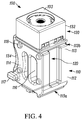
- FIG. 4 is a perspective view of the camera module and shock assembly of FIG. 3 in accordance with some embodiments.
- FIG. 5 is a first side perspective view of the camera module and shock assembly of FIGS. 3 and 4 and a shield member prior to being mounted to a printed circuit board of the barcode or optical reading device of FIGS. 1-4 in accordance with some embodiments.
- FIG. 6 is a second side perspective view of the camera module, shock assembly, and shield member of FIG. 5 prior to being mounted to the printed circuit board of the barcode or optical reading device of FIGS. 1-5 in accordance with some embodiments.
- FIG. 7 is a cross-sectional view of the camera module, shock assembly, and shield member of FIGS. 5 and 6 prior to mounting the shield member to the printed circuit board in accordance with some embodiments.
- FIG. 8 is a cross-sectional view of the camera module, shock assembly, and shield member of FIGS. 5-7 upon mounting the shield member to the printed circuit board in accordance with some embodiments.
- FIG. 9 is a perspective view of the camera module and shock assembly of FIGS. 1-8 prior to mounting the frame member to the printed circuit board in accordance with some embodiments.
- FIG. 10 is a cross-sectional view of the camera module and shock assembly of FIGS. 1-9 upon mounting the frame member to the printed circuit board in accordance with some embodiments.
- FIG. 11 is a first side perspective view of the example barcode or optical reading device of FIGS. 1-10 in a partially assembled state in accordance with some embodiments.
- FIG. 12 is a second side perspective view of the example barcode or optical reading device of FIGS. 1-11 in a partially assembled state in accordance with some embodiments.
- FIG. 13 is a bottom plan view of the example barcode or optical reading device of FIGS. 1-12 in an assembled state in accordance with some embodiments.
- FIG. 14 is a cross-sectional front elevation view of the example barcode or optical reading device of FIGS. 1-13 in an assembled state in accordance with some embodiments.
- the present application provides a scanning assembly for scanning at least one object appearing in a field of view includes a circuit board, a shock assembly adjacent to the circuit board, a scanning module defining a scanning axis defined along a first side of the module, a shielding assembly at least partially surrounding the scanning module, and a frame assembly including at least one opening to accommodate at least a portion of the shielding assembly.
- the scanning module is operably coupled to the shock assembly such that the shock assembly is disposed between the scanning module and the circuit board.
- the frame restricts movement of the scanning module and the shielding assembly.
- the scanning module and the shock assembly are movable in a direction parallel to the scanning axis, and the shock assembly is adapted to dampen a force exerted by the scanning module on the circuit board.
- the present disclosure includes a scanner for scanning at least one object appearing in a FOV.
- the scanner includes a housing, a circuit board fixedly mounted relative to the housing, a frame assembly including at least one opening and being fixedly mounted relative to the housing, a shock assembly positioned adjacent to the circuit board, a scanning module defining a scanning axis defined along a first side of the module, and a shielding assembly.
- the scanning module is movably mounted relative to the housing and being operably coupled to the shock assembly.
- the shielding assembly at least partially surrounds the scanning module, the shielding assembly being fixedly mounted relative to the housing. At least a portion of the scanning module and the shielding assembly are disposed adjacent to the at least one opening in the frame assembly such that the frame assembly restricts movement of the scanning module and the shielding assembly.
- the barcode or optical reading device 100 includes a printed circuit board 102 , a shock assembly 110 , a scanning module 130 , a shielding assembly 140 , and a frame assembly 160 .
- the device 100 may be disposed within a shell or housing 101 defining an opening 101 a therethrough.
- the printed circuit board 102 may accommodate a memory and a controller that controls operation of the device 100 . It should be appreciated that the device 100 may include any number of additional components such as decoding systems, processors, and/or circuitry coupled to the circuit board 102 to assist in operation of the device 100 .
- the shock assembly 110 is positioned adjacent to the printed circuit board 102 .
- the shock assembly 110 may include a shock absorber 112 and a gasket member 126 having a proximal end 126 a disposed adjacent to the printed circuit board 102 and further having a distal end 126 b .
- the shock absorber 112 defines an elongated body 113 having a proximal end 113 a and a distal end 113 b .
- the proximal end 113 a of the elongated body 113 is positioned adjacent to the printed circuit board 102 .
- the elongated body of the shock absorber 112 defines an indentation 114 , any number of cut outs 116 , and any number of tabs 117 and contact protrusions 118 extending from the elongated body 113 . Further, the elongated body 113 may define an elongated groove 120 formed thereon.
- the shock absorber 112 and/or the gasket member 126 may be constructed from any number of suitable resilient materials and/or combinations of materials such as, for example, a rubber material or a foam material capable of flexing and/or temporarily deforming to absorb a shock. Other examples are possible.
- the scanning module 130 defines a first side 130 a and a second side 130 b .
- a scanning axis “L” is defined along the first side 130 a of the scanning module 130 .
- the scanning module 130 may be in the form of a camera or a laser scanner 132 which may include any number of components such as lenses, mirrors, and the like. Other examples are possible.
- the scanning module 130 additionally includes a data transfer cable 134 coupled to the camera or laser scanner 132 to electrically couple the printed circuit board 102 to the scanning module 130 .
- the data transfer cable 134 may be in the form of a flat printed circuit cable. Any number of suitable cables and/or connections may be used.
- the scanning module 130 is operably coupled to the shock assembly 110 .
- the camera or laser scanner 132 is positioned at the distal end 113 b of the elongated body 113 such that first side 130 a of the scanning module is disposed against or near the shock assembly 110 .
- the shock assembly 110 is disposed between the scanning module 130 and the printed circuit board 102 .
- the scanning module 130 may be secured to the shock assembly 110 via an adhesive 103 such as a tape.
- the indentation 114 formed in the elongated body 113 of the shock absorber 112 accommodates a portion of the data transfer cable 134 .
- the shielding assembly 140 is adapted to at least partially surround the scanning module 130 .
- the shielding assembly 140 includes a shield member or shell 141 and a cage member 150 .
- the shell 141 has a proximal end 141 a and a distal end 141 b , a first opening 142 formed at the proximal end 141 a of the shell 141 , a second opening 143 formed at the distal end 141 b of the shell 141 , a first tab 144 extending inwardly into the shell 141 , a second tab 145 extending outwardly from the shell 141 , a first ledge or shoulder portion 146 defined near the proximal end 141 a of the shell 141 , and a second ledge or shoulder portion 147 defined near the distal end 141 b of the shell 141 .
- the cage member 150 is defined by a body 151 having a proximal end 151 a and a distal end 151 b .
- the body 151 of the cage member 150 further includes a plurality of inwardly-disposed retention portions 152 which, in the illustrated embodiment, are in the form of curled ledges, and further includes a slot 154 formed in the body 151 .
- the proximal end 151 a of the body 151 is coupled to the printed circuit board 102 via any number of approaches such as, for example, via soldering or similar techniques.
- the frame assembly 160 may be a rigid or semi-rigid member that is operably coupled to the printed circuit board 102 and/or the housing 101 to align and secure the components mounted to the printed circuit board 102 .
- the frame assembly 160 may include a number of mounting holes 160 a that align with mounting holes 102 a formed by the printed circuit board 102 . Any number of screws 104 may be used to secure the frame member 160 to the printed circuit board 102 .
- the frame assembly 160 includes an elevated portion 164 defining a ledge 165 and an opening 166 positioned adjacent or near the ledge 165 .
- the camera or laser scanner 132 of the scanning module 130 is operably coupled to the distal end 113 b of the elongated body 113 of the shock absorber 112 via the adhesive 103 or other coupling mechanism.
- the data transfer cable 134 is wrapped around the elongated body 113 of the shock absorber 112 and positioned at the proximal end 113 a thereof.
- an adhesive 103 may be placed on the proximal end 113 a of the elongated body 133 to secure the data transfer cable 134 thereto (as illustrated in FIG. 4 ).
- the proximal end 151 a of the cage member 150 body 151 is coupled to the printed circuit board 102 via soldering or any other approach.
- the gasket member 126 is placed inside the cage member 150 such that the proximal end 126 a of the gasket member 126 abuts and/or is near the printed circuit board 102 .
- the proximal end 151 a of the cage member 150 may define a ledge 151 c that supports the gasket member 126 . As such, the gasket member 126 positively grounds the shield member 141 .
- the shock absorber 112 (along with the scanning module 130 ) is then placed into the opening formed by the gasket member 126 , whereby a connector of the data transfer cable 134 is inserted into a port on the printed circuit board 102 .
- the tabs 117 of the shock absorber 112 are positioned adjacent to or near the distal end 126 b of the gasket 126 .
- the shield member 141 of the shielding assembly 140 is then properly aligned with the shock assembly 110 prior to installation. Specifically, the first tab 144 of the shield member 141 is aligned with the elongated groove 120 of the shock absorber 112 . Additionally, the second tab 145 of the shield member 141 is aligned with the slot 154 of the cage member 150 . The alignment between the shield member 141 and the shock absorber 112 and cage member 150 ensure a proper assembly orientation between these components, thus reducing the possibility of misalignment.
- the first tab 144 of the shield member 141 slides down the elongated groove 120 of the shock absorber 112 .
- the second tab 145 of the shield member 141 is inserted into the slot 154 of the cage member 150 .
- the retention portions 152 flex outwardly to allow the first shoulder portion 146 disposed at the proximal end 141 a of the shield member 141 to be inserted.
- the retention portions 152 Upon the retention portions 152 traversing the first shoulder portion 146 of the shield member, the retention portions 152 return to an initial configuration that may assist in clamping, securing, and/or retaining the shield member 141 in place at the first shoulder portion 146 .
- the body 151 of the cage member 150 may also assist in retaining the shield member 141 .
- the shield member 141 may be coupled to the shock assembly 110 and/or the scanning module 130 via any number of additional approaches. Additionally, the first shoulder portion 146 of the shield member 141 rests on the tabs 117 of the shock absorber 112 to maintain a gap that accommodates a portion of the data transfer cable 134 .
- the scanning module 130 When the shield member 141 is installed, the scanning module 130 is disposed adjacent to the second opening 143 at the distal end 141 b of the shield member 141 . As a result, the camera or laser scanner 132 may capture images within its FOV through the second opening 143 . In this configuration, the shield member 141 is additionally aligned by abutting against the contact protrusions 118 on the elongated body 113 . This configuration properly positions the camera or laser scanner 132 in the center of the second opening 143 of the shield member 141 .
- the shield member 141 combined with the cage member 150 and/or the gasket member 126 , provide complete shielding of EMI generated by the scanning module 130 , while the shock assembly 110 and/or the gasket member 126 provides a cushion for both the circuit board 102 and the scanning module 130 against the device being dropped and/or otherwise jostled.
- the frame assembly 160 is secured to the printed circuit board 102 using any number of approaches (e.g., by inserting the screws 104 into the mounting holes 162 , 102 a of the frame assembly 160 and printed circuit board 102 , respectively).
- the frame assembly 160 is positioned such that at least a portion of the scanning module 140 (e.g., the camera or laser scanner 132 ) and a portion of the shielding assembly 141 (e.g., the distal end 141 b ) are adjacent to and/or disposed through the opening 166 in the frame assembly 160 .
- the scanning module 140 e.g., the camera or laser scanner 132
- the shielding assembly 141 e.g., the distal end 141 b
- the frame assembly 160 Upon mounting the frame assembly 160 , the ledge 165 of the frame assembly 160 contacts the second shoulder portion 147 of the shield member 141 . As a result, the frame assembly 160 restricts movement of the shock assembly 110 , the scanning module 130 , and the shielding assembly 140 in directions that are not generally parallel to the imaging axis L. As such, the frame assembly 160 provides accurate alignment to the opening or camera window 101 a on the housing 101 without requiring a substantial number of parts in the tolerance chain. At the same time, the shock assembly 110 , the scanning module 130 , and the shielding assembly 140 are permitted to move in a direction generally parallel to the scanning axis L.
- a gap may be present between the ledge 165 of the frame assembly and the second shoulder portion 147 of the shield member 141 to further accommodate relative movement in the direction generally parallel to the imaging axis L.
- the gap may be between approximately 0.1 mm and approximately 5.0 mm. Other examples are possible.
- the shock assembly 110 dampens any forces exerted by the scanning module 130 on the printed circuit board 102 by compressing the elongated body 113 of the shock assembly 110 .
- the cut outs 116 disposed on the elongated body 113 of the shock absorber 110 assist in cushioning and dampening any forces experienced upon compression of the elongated body 113 .
- the indentation 114 accommodates a portion of the data transfer cable 134 to prevent the data transfer cable 134 from becoming pinched or damaged, thereby reducing additional stresses on the printed circuit board 102 .
- the shield member 141 prevents emissions that could impact the function of the circuit board 102
- the gasket member 126 will remain in contact with the shield member 141 and thereby provides shielding even in the event of a drop. As a result, the RF performance of the device 100 is not impacted, thus reducing and/or eliminating a risk of interruption to data transfer during a drop.
- assembly of the device 100 further includes installing additional components such as a flash assembly 105 , any additional baffles 106 , sensors 107 , lenses 108 , and the like. These components are then enclosed by the housing 101 .
- the opening 101 a of the housing is positioned to be aligned with the opening 166 of the frame assembly 160 , the second opening 143 of the shield member 141 , and the camera or laser scanner 132 such that these components are axially aligned to provide a FOV for the camera or laser scanner 132 .
- a includes . . . a”, “contains . . . a” does not, without more constraints, preclude the existence of additional identical elements in the process, method, article, or apparatus that comprises, has, includes, contains the element.
- the terms “a” and “an” are defined as one or more unless explicitly stated otherwise herein.
- the terms “substantially”, “essentially”, “approximately”, “about” or any other version thereof, are defined as being close to as understood by one of ordinary skill in the art, and in one non-limiting embodiment the term is defined to be within 10%, in another embodiment within 5%, in another embodiment within 1% and in another embodiment within 0.5%.
- the term “coupled” as used herein is defined as connected, although not necessarily directly and not necessarily mechanically.
- a device or structure that is “configured” in a certain way is configured in at least that way, but may also be configured in ways that are not listed.
- processors such as microprocessors, digital signal processors, customized processors and field programmable gate arrays (FPGAs) and unique stored program instructions (including both software and firmware) that control the one or more processors to implement, in conjunction with certain non-processor circuits, some, most, or all of the functions of the method and/or apparatus described herein.
- processors or “processing devices” such as microprocessors, digital signal processors, customized processors and field programmable gate arrays (FPGAs) and unique stored program instructions (including both software and firmware) that control the one or more processors to implement, in conjunction with certain non-processor circuits, some, most, or all of the functions of the method and/or apparatus described herein.
- FPGAs field programmable gate arrays
- unique stored program instructions including both software and firmware
- an embodiment can be implemented as a computer-readable storage medium having computer readable code stored thereon for programming a computer (e.g., comprising a processor) to perform a method as described and claimed herein.
- Examples of such computer-readable storage mediums include, but are not limited to, a hard disk, a CD-ROM, an optical storage device, a magnetic storage device, a ROM (Read Only Memory), a PROM (Programmable Read Only Memory), an EPROM (Erasable Programmable Read Only Memory), an EEPROM (Electrically Erasable Programmable Read Only Memory) and a Flash memory.
Landscapes
- Physics & Mathematics (AREA)
- General Physics & Mathematics (AREA)
- Electromagnetism (AREA)
- Engineering & Computer Science (AREA)
- Optics & Photonics (AREA)
- Microelectronics & Electronic Packaging (AREA)
- Health & Medical Sciences (AREA)
- General Health & Medical Sciences (AREA)
- Toxicology (AREA)
- Artificial Intelligence (AREA)
- Computer Vision & Pattern Recognition (AREA)
- Theoretical Computer Science (AREA)
- Studio Devices (AREA)
Abstract
Description
Claims (21)
Priority Applications (1)
| Application Number | Priority Date | Filing Date | Title |
|---|---|---|---|
| US16/180,205 US10816793B2 (en) | 2018-11-05 | 2018-11-05 | Floating EMI shield |
Applications Claiming Priority (1)
| Application Number | Priority Date | Filing Date | Title |
|---|---|---|---|
| US16/180,205 US10816793B2 (en) | 2018-11-05 | 2018-11-05 | Floating EMI shield |
Publications (2)
| Publication Number | Publication Date |
|---|---|
| US20200142185A1 US20200142185A1 (en) | 2020-05-07 |
| US10816793B2 true US10816793B2 (en) | 2020-10-27 |
Family
ID=70457750
Family Applications (1)
| Application Number | Title | Priority Date | Filing Date |
|---|---|---|---|
| US16/180,205 Active 2039-07-05 US10816793B2 (en) | 2018-11-05 | 2018-11-05 | Floating EMI shield |
Country Status (1)
| Country | Link |
|---|---|
| US (1) | US10816793B2 (en) |
Families Citing this family (2)
| Publication number | Priority date | Publication date | Assignee | Title |
|---|---|---|---|---|
| US20210325683A1 (en) * | 2020-09-02 | 2021-10-21 | Facebook Technologies, Llc | Virtual reality systems and methods |
| US12229627B1 (en) * | 2023-08-01 | 2025-02-18 | Datalogic Ip Tech S.R.L. | Scanner camera with PCB-integrated lens holder |
Citations (3)
| Publication number | Priority date | Publication date | Assignee | Title |
|---|---|---|---|---|
| US20170118408A1 (en) * | 2015-10-22 | 2017-04-27 | Apple Inc. | Inductive three-axis lens position measurement using af and ois coils |
| US9891445B1 (en) * | 2014-09-05 | 2018-02-13 | Apple Inc. | Passive damping solution to optical image stabilization for voice coil motors |
| US20190104239A1 (en) * | 2016-03-02 | 2019-04-04 | Optotune Consumer Ag | Optical device, particularly camera, particularly comprising autofocus, image stabilization and super resolution |
-
2018
- 2018-11-05 US US16/180,205 patent/US10816793B2/en active Active
Patent Citations (3)
| Publication number | Priority date | Publication date | Assignee | Title |
|---|---|---|---|---|
| US9891445B1 (en) * | 2014-09-05 | 2018-02-13 | Apple Inc. | Passive damping solution to optical image stabilization for voice coil motors |
| US20170118408A1 (en) * | 2015-10-22 | 2017-04-27 | Apple Inc. | Inductive three-axis lens position measurement using af and ois coils |
| US20190104239A1 (en) * | 2016-03-02 | 2019-04-04 | Optotune Consumer Ag | Optical device, particularly camera, particularly comprising autofocus, image stabilization and super resolution |
Also Published As
| Publication number | Publication date |
|---|---|
| US20200142185A1 (en) | 2020-05-07 |
Similar Documents
| Publication | Publication Date | Title |
|---|---|---|
| KR101428842B1 (en) | Camera module for Vehicle | |
| US10222577B2 (en) | Lens driving device, camera module, and camera mount device | |
| CN114690364B (en) | Lens drive motors, camera modules and mobile phones | |
| US11493779B2 (en) | Optical unit with shake correction function | |
| US10816793B2 (en) | Floating EMI shield | |
| KR102722836B1 (en) | Optical arrangements for small size wide angle auto focus imaging lens for high resolution sensors | |
| US20250389936A1 (en) | Optical Arrangement for Small Size Wide Angle Auto Focus Imaging Lens for High Resolution Sensors | |
| CN107111093A (en) | Lens driver, camara module and camera carrying device | |
| KR102608087B1 (en) | Lens drive devices, camera modules, and camera mounting devices | |
| JP7028589B2 (en) | Imaging device | |
| JP6793581B2 (en) | Imaging device | |
| JP2018174361A (en) | Imaging device | |
| JP2019208190A (en) | Imaging apparatus | |
| US10466573B2 (en) | Camera lens assembly | |
| US12401871B2 (en) | Vehicular camera | |
| KR20240034733A (en) | A camera module and optical apparatus having the same | |
| JP2018164189A (en) | Imaging apparatus | |
| JP7161472B2 (en) | Imaging device | |
| WO2019067916A1 (en) | Imaging devices having progressive magnification | |
| US20110101100A1 (en) | Support assembly for terminal | |
| KR102116567B1 (en) | Camera module | |
| KR102005479B1 (en) | Camera module |
Legal Events
| Date | Code | Title | Description |
|---|---|---|---|
| FEPP | Fee payment procedure |
Free format text: ENTITY STATUS SET TO UNDISCOUNTED (ORIGINAL EVENT CODE: BIG.); ENTITY STATUS OF PATENT OWNER: LARGE ENTITY |
|
| AS | Assignment |
Owner name: ZIH CORP., ILLINOIS Free format text: ASSIGNMENT OF ASSIGNORS INTEREST;ASSIGNORS:MAO, YANMIN;PALPUNURI, RAMANA REDDY;REEL/FRAME:049265/0975 Effective date: 20190521 |
|
| AS | Assignment |
Owner name: JPMORGAN CHASE BANK, N.A., AS COLLATERAL AGENT, NEW YORK Free format text: SECURITY INTEREST;ASSIGNOR:ZEBRA TECHNOLOGIES CORPORATION;REEL/FRAME:049674/0916 Effective date: 20190701 |
|
| AS | Assignment |
Owner name: ZEBRA TECHNOLOGIES CORPORATION, ILLINOIS Free format text: MERGER;ASSIGNOR:ZIH CORP.;REEL/FRAME:049844/0929 Effective date: 20181220 |
|
| AS | Assignment |
Owner name: JPMORGAN CHASE BANK, N.A., NEW YORK Free format text: SECURITY INTEREST;ASSIGNORS:ZEBRA TECHNOLOGIES CORPORATION;LASER BAND, LLC;TEMPTIME CORPORATION;REEL/FRAME:053841/0212 Effective date: 20200901 |
|
| STPP | Information on status: patent application and granting procedure in general |
Free format text: NOTICE OF ALLOWANCE MAILED -- APPLICATION RECEIVED IN OFFICE OF PUBLICATIONS |
|
| STCF | Information on status: patent grant |
Free format text: PATENTED CASE |
|
| AS | Assignment |
Owner name: LASER BAND, LLC, ILLINOIS Free format text: RELEASE OF SECURITY INTEREST - 364 - DAY;ASSIGNOR:JPMORGAN CHASE BANK, N.A.;REEL/FRAME:056036/0590 Effective date: 20210225 Owner name: TEMPTIME CORPORATION, NEW JERSEY Free format text: RELEASE OF SECURITY INTEREST - 364 - DAY;ASSIGNOR:JPMORGAN CHASE BANK, N.A.;REEL/FRAME:056036/0590 Effective date: 20210225 Owner name: ZEBRA TECHNOLOGIES CORPORATION, ILLINOIS Free format text: RELEASE OF SECURITY INTEREST - 364 - DAY;ASSIGNOR:JPMORGAN CHASE BANK, N.A.;REEL/FRAME:056036/0590 Effective date: 20210225 |
|
| MAFP | Maintenance fee payment |
Free format text: PAYMENT OF MAINTENANCE FEE, 4TH YEAR, LARGE ENTITY (ORIGINAL EVENT CODE: M1551); ENTITY STATUS OF PATENT OWNER: LARGE ENTITY Year of fee payment: 4 |