US10811775B2 - Loop antenna - Google Patents
Loop antenna Download PDFInfo
- Publication number
- US10811775B2 US10811775B2 US16/244,299 US201916244299A US10811775B2 US 10811775 B2 US10811775 B2 US 10811775B2 US 201916244299 A US201916244299 A US 201916244299A US 10811775 B2 US10811775 B2 US 10811775B2
- Authority
- US
- United States
- Prior art keywords
- segment
- grounding
- radiating
- loop antenna
- grounding segment
- Prior art date
- Legal status (The legal status is an assumption and is not a legal conclusion. Google has not performed a legal analysis and makes no representation as to the accuracy of the status listed.)
- Active, expires
Links
- 239000000758 substrate Substances 0.000 claims abstract description 11
- 238000010586 diagram Methods 0.000 description 15
- 230000005855 radiation Effects 0.000 description 4
- 239000003990 capacitor Substances 0.000 description 3
- XEEYBQQBJWHFJM-UHFFFAOYSA-N Iron Chemical compound [Fe] XEEYBQQBJWHFJM-UHFFFAOYSA-N 0.000 description 2
- 239000004020 conductor Substances 0.000 description 2
- RYGMFSIKBFXOCR-UHFFFAOYSA-N Copper Chemical compound [Cu] RYGMFSIKBFXOCR-UHFFFAOYSA-N 0.000 description 1
- BQCADISMDOOEFD-UHFFFAOYSA-N Silver Chemical compound [Ag] BQCADISMDOOEFD-UHFFFAOYSA-N 0.000 description 1
- 239000000956 alloy Substances 0.000 description 1
- 229910045601 alloy Inorganic materials 0.000 description 1
- 229910052782 aluminium Inorganic materials 0.000 description 1
- XAGFODPZIPBFFR-UHFFFAOYSA-N aluminium Chemical compound [Al] XAGFODPZIPBFFR-UHFFFAOYSA-N 0.000 description 1
- 229910052802 copper Inorganic materials 0.000 description 1
- 239000010949 copper Substances 0.000 description 1
- 229910052742 iron Inorganic materials 0.000 description 1
- 229910052751 metal Inorganic materials 0.000 description 1
- 239000007769 metal material Substances 0.000 description 1
- 229910052709 silver Inorganic materials 0.000 description 1
- 239000004332 silver Substances 0.000 description 1
Images


Classifications
-
- H—ELECTRICITY
- H01—ELECTRIC ELEMENTS
- H01Q—ANTENNAS, i.e. RADIO AERIALS
- H01Q7/00—Loop antennas with a substantially uniform current distribution around the loop and having a directional radiation pattern in a plane perpendicular to the plane of the loop
- H01Q7/005—Loop antennas with a substantially uniform current distribution around the loop and having a directional radiation pattern in a plane perpendicular to the plane of the loop with variable reactance for tuning the antenna
-
- H—ELECTRICITY
- H01—ELECTRIC ELEMENTS
- H01Q—ANTENNAS, i.e. RADIO AERIALS
- H01Q1/00—Details of, or arrangements associated with, antennas
- H01Q1/12—Supports; Mounting means
- H01Q1/22—Supports; Mounting means by structural association with other equipment or articles
- H01Q1/2258—Supports; Mounting means by structural association with other equipment or articles used with computer equipment
- H01Q1/2266—Supports; Mounting means by structural association with other equipment or articles used with computer equipment disposed inside the computer
-
- H—ELECTRICITY
- H01—ELECTRIC ELEMENTS
- H01Q—ANTENNAS, i.e. RADIO AERIALS
- H01Q1/00—Details of, or arrangements associated with, antennas
- H01Q1/36—Structural form of radiating elements, e.g. cone, spiral, umbrella; Particular materials used therewith
- H01Q1/38—Structural form of radiating elements, e.g. cone, spiral, umbrella; Particular materials used therewith formed by a conductive layer on an insulating support
-
- H—ELECTRICITY
- H01—ELECTRIC ELEMENTS
- H01Q—ANTENNAS, i.e. RADIO AERIALS
- H01Q5/00—Arrangements for simultaneous operation of antennas on two or more different wavebands, e.g. dual-band or multi-band arrangements
- H01Q5/30—Arrangements for providing operation on different wavebands
- H01Q5/307—Individual or coupled radiating elements, each element being fed in an unspecified way
- H01Q5/314—Individual or coupled radiating elements, each element being fed in an unspecified way using frequency dependent circuits or components, e.g. trap circuits or capacitors
- H01Q5/328—Individual or coupled radiating elements, each element being fed in an unspecified way using frequency dependent circuits or components, e.g. trap circuits or capacitors between a radiating element and ground
Definitions
- the present disclosure relates to an antenna element, and particularly, to a loop antenna.
- Built-in antennas such as dipole antennas, planar inverted-F antennas (PIFA), or loop antennas, are generally applied to mobile devices such as notebook computers, tablet computers, or mobile phones, and particular antenna space needs to be reserved in internal space of the devices.
- PIFA planar inverted-F antennas
- loop antennas are generally applied to mobile devices such as notebook computers, tablet computers, or mobile phones, and particular antenna space needs to be reserved in internal space of the devices.
- a loop antenna includes a substrate, and a grounding portion, a radiating portion, a matching portion, and a feeding portion that are located on the substrate.
- the grounding portion includes a first grounding segment and a second grounding segment.
- the second grounding segment is perpendicular to the first grounding segment, and a first end of the second grounding segment is connected to a first end of the first grounding segment.
- the radiating portion includes a first radiating segment and a second radiating segment. The first radiating segment is connected to a second end of the first grounding segment and extending from the first grounding segment towards a direction away from the first grounding segment.
- the second radiating segment is connected to the first radiating segment and extending from the first radiating segment towards a direction facing the second grounding segment.
- the matching portion is located at an end of the second radiating segment close to the second grounding segment.
- the feeding portion is located between the end of the second radiating segment close to the second grounding segment, and is located between the matching portion and the second grounding segment.
- the feeding portion is configured to receive and transmit a feeding signal from a signal source.
- FIG. 1 is a schematic diagram of an embodiment of a loop antenna according to the present disclosure
- FIG. 2 is a schematic diagram of a size of the loop antenna in FIG. 1 ;
- FIG. 3 is a diagram of return loss of an embodiment of a loop antenna at each operating frequency according to the present disclosure
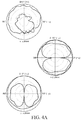
- FIG. 4A is radiation patterns of an embodiment of a loop antenna operated at 2.4 GHz according to the present disclosure
- FIG. 4B is a radiation pattern of an embodiment of a loop antenna operated at 5.8 GHz according to the present disclosure
- FIG. 5 is a schematic diagram of an embodiment of a matching portion of a loop antenna according to the present disclosure.
- FIG. 6 is a diagram of return loss of the loop antenna in FIG. 5 ;
- FIG. 7 is another diagram of return loss of the loop antenna in FIG. 5 ;
- FIG. 8 is a schematic diagram of another embodiment of a loop antenna according to the present disclosure.
- FIG. 9 is a schematic diagram of an embodiment of a loop antenna applied to an electronic device according to the present disclosure.
- FIG. 1 is a schematic diagram of an embodiment of a loop antenna 1 according to the present disclosure.
- the loop antenna 1 has lower-frequency and higher-frequency resonant modes.
- the loop antenna 1 includes a substrate 10 , and a radiating portion 11 , a matching portion 13 , and a grounding portion 14 that are located on the substrate 10 .
- the radiating portion 11 , the grounding portion 14 , and the feeding portion 12 are made of conductive materials (for example, copper, silver, iron, or aluminum, or an alloy thereof), and the radiating portion 11 and the grounding portion 14 are printed on the substrate 10 .
- the grounding portion 14 is configured to provide signal grounding, and the grounding portion 14 is connected to a system ground plane of an electronic device having the loop antenna 1 .
- the grounding portion 14 includes a first grounding segment 141 and a second grounding segment 142 .
- a first end 142 A of the second grounding segment 142 is connected to a first end 141 A of the first grounding segment 141 , and the first grounding segment 141 is perpendicular to the second grounding segment 142 (where for example, a length direction of the first grounding segment 141 is perpendicular to a length direction of the second grounding segment 142 ).
- the first grounding segment 141 and the second grounding segment 142 are of an inverted-L shape.
- the radiating portion 11 includes a first radiating segment 111 and a second radiating segment 112 .
- a second end 111 B of the first radiating segment 111 is connected to a second end 141 B of the first grounding segment 141
- the first radiating segment 111 is extending from the first grounding segment 141 towards a direction away from the first grounding segment 141
- a first end 111 A of the first radiating segment 111 is connected to a first end 112 A of the second radiating segment 112 .
- the second radiating segment 112 extends from the first radiating segment 111 towards a direction facing the second grounding segment 142 of the grounding portion 14 .
- the matching portion 13 is located at an end (that is, a second end 112 B) of the second radiating segment 112 close to the second grounding segment 142 .
- the matching portion 13 is implemented using a passive element, and the matching portion 13 excites the loop antenna 1 to generate a resonant mode of less than or equal to 0.25 wavelength at the lower-frequency.
- the feeding portion 12 is located between the second end 112 B of the second radiating segment 112 and the second grounding segment 142 , and the feeding portion 12 is located between the matching portion 13 and the second grounding segment 142 .
- the feeding portion 12 is configured to receive or transmit a feeding signal from a signal source and form a closed current resonant path between the radiating portion 11 and the grounding portion 14 . Therefore, when the feeding signal is fed from the feeding portion 12 , the loop antenna 1 generates the resonant mode of less than or equal to 0.25 wavelength at the lower-frequency by the matching portion 13 .
- the loop antenna 1 is capable of operating in a lower-frequency band (0.25 wavelength) and a higher frequency band (0.5 wavelength), thereby satisfying a requirement of a current electronic communication device.
- the loop antenna 1 has a length direction D 1 and a width direction D 2 .
- a length L 2 of the radiating portion 11 in the length direction D 1 ranges between 16.5 mm and 17.5 mm, and a line width W 1 of the radiating portion 11 in the width direction D 2 ranges between 3 mm and 4 mm.
- a length L 1 of the first grounding segment 141 in the length direction D 1 is 20 mm, and a line width W 2 of the first grounding segment 141 in the width direction D 2 ranges between 1 mm and 2 mm.
- a length L 3 of the second grounding segment 142 in the length direction D 1 is 2 mm, and a line width W 3 of the second grounding segment 142 in the width direction D 2 is 5 mm.
- a length L 4 of the feeding portion 12 in the length direction D 1 is 0.5 mm. Based on the foregoing, an overall length of the loop antenna 1 in the length direction D 1 is 20 mm, and an overall width of the loop antenna 1 in the width direction D 2 is 5 mm (where a sum of the line width W 2 of the first grounding segment 141 in the width direction D 2 and the line width W 1 of the radiating portion 11 in the width direction D 2 does not exceed 5 mm).
- an overall size of the loop antenna 1 is 20 mm ⁇ 5 mm (that is, 100 mm 2 ).
- the size of the loop antenna 1 satisfies a requirement on an electronic device having a narrow bezel (for example, a narrow bezel of 5 mm to 7 mm width).
- FIG. 3 is a diagram of return loss of an embodiment of the loop antenna 1 at each operating frequency according to the present disclosure. It is learned in FIG. 3 that the lower-frequency band and the higher-frequency band in which the loop antenna 1 is capable of operating respectively cover the 2.4 GHz and 5.8 GHz bands. Further, referring to FIG. 4A and FIG. 4B , FIG. 4A and FIG. 4B are respectively radiation patterns of the loop antenna 1 operating in the frequency bands of 2.4 GHz and 5.8 GHz. It is learned from pattern distribution shown in FIG. 4A and FIG. 4B that when the loop antenna 1 is operating at 2.4 GHz and 5.8 GHz, an antenna gain in each direction is desirable.
- the first radiating segment 111 is perpendicular to the second radiating segment 112 (that is, a length direction of the first radiating segment 111 is perpendicular to a length direction of the second radiating segment 112 ). That is, the first radiating segment 111 and the second radiating segment 112 forms an inverted-L shape, and the inverted L-shape of the first grounding segment 141 , the second grounding segment 142 , the feeding portion 12 , and the matching portion 13 form the closed current path.
- the second radiating segment 112 is parallel to the first grounding segment 141 and is perpendicular to the second grounding segment 142
- the first radiating segment 111 is parallel to the second grounding segment 142 and is perpendicular to the first grounding segment 141 .
- the matching portion 13 includes a chip capacitor, to excite the lower-frequency resonant mode of the loop antenna 1 by the chip capacitor.
- the matching portion 13 includes two matching elements disposed at an interval.
- FIG. 5 is a schematic diagram of an embodiment of the matching portion 13 of the loop antenna 1 according to the present disclosure. As shown in FIG. 5 , the matching portion 13 includes matching elements 131 and 132 disposed at an interval. The matching element 132 is located between the matching element 131 and the feeding portion 12 , and the matching element 132 is closer to the feeding portion 12 than the matching element 131 .
- the matching elements 131 and 132 are respectively a chip inductor and a chip capacitor.
- An inductance value of the matching element 131 ranges between 4.2 nH and 5.3 nH, and a capacitance value of the matching element 132 ranges between 0.1 pF and 0.3 pF. Further, lengths L 5 and L 6 of the matching elements 131 and 132 in the length direction D 1 are 0.6 mm, and an interval G 1 between the matching elements 131 and 132 and an interval G 2 between the matching element 132 and the feeding portion 12 are 1 mm.
- the matching element 132 is capable of exciting the lower-frequency resonant mode of the loop antenna 1
- the matching element 131 is capable of controlling an operating frequency of the loop antenna 1 in the higher-frequency resonant mode, so that the operating frequencies of the loop antenna 1 respectively cover the 2.4 GHz and 5.8 GHz bands.
- FIG. 6 and FIG. 7 are respectively a diagram of return loss of the loop antenna 1 including the matching element 132 having a different capacitance value at each operating frequency and a diagram of return loss of the loop antenna 1 including the matching element 131 having a different inductance value at each operating frequency.
- Return loss curves 61 , 62 , and 63 respectively correspond to the loop antenna 1 including the matching element 131 having capacitance values 0.3 pF, 0.2 pF, and 0.1 pF
- return loss curves 71 , 72 , and 73 respectively correspond to the loop antenna 1 including the matching element 131 having inductance values 4.2 nH, 4.8 nH, and 5.3 nH. It is learned in FIG. 6 that a larger capacitance value of the matching element 132 indicates a lower operating frequency of the loop antenna 1 in the lower-frequency resonant mode. It is learned in FIG. 7 that a smaller inductance value of the matching element 131 indicates a higher operating frequency of the loop antenna 1 in the higher-frequency resonant mode.
- FIG. 8 is a schematic diagram of another embodiment of a loop antenna according to the present disclosure.
- the grounding portion 14 further includes a third grounding segment 143 in addition to the first grounding segment 141 and the second grounding segment 142 .
- the third grounding segment 143 is connected to the second grounding segment 142 , and the third grounding segment 143 is extending from the second grounding segment 142 towards a direction facing the second radiating segment 112 .
- the feeding portion 12 is located between the matching portion 13 and the third grounding segment 143 .
- the loop antenna 1 shown in FIG. 8 also has lower-frequency and higher-frequency resonant modes.
- FIG. 9 is a schematic diagram of an embodiment of a loop antenna applied to an electronic device 2 according to the present disclosure.
- a notebook computer is used as an example of the electronic device 2 shown in FIG. 9 , but the present disclosure is not thereto.
- the electronic device 2 is alternatively a tablet computer or an all-in-one (AiO) computer.
- the size of the loop antenna 1 is 5 mm ⁇ 20 mm, and the loop antenna 1 is disposed in a narrow bezel around a screen of the electronic device 2 , to satisfy a requirement on a current electronic device having a narrow bezel.
- the low-frequency resonant mode of the loop antenna is further excited by using the matching portion, so that the loop antenna is capable of operating in at least two frequency bands: the low frequency and the high frequency.
- the size of the loop antenna is 5 mm ⁇ 20 mm, satisfying a requirement on an existing electronic device having a narrow bezel.
Landscapes
- Engineering & Computer Science (AREA)
- Computer Hardware Design (AREA)
- General Engineering & Computer Science (AREA)
- Details Of Aerials (AREA)
- Support Of Aerials (AREA)
Abstract
Description
Claims (10)
Applications Claiming Priority (3)
| Application Number | Priority Date | Filing Date | Title |
|---|---|---|---|
| TW107108923 | 2018-03-15 | ||
| TW107108923A TWI667844B (en) | 2018-03-15 | 2018-03-15 | Loop antenna |
| TW107108923A | 2018-03-15 |
Publications (2)
| Publication Number | Publication Date |
|---|---|
| US20190288395A1 US20190288395A1 (en) | 2019-09-19 |
| US10811775B2 true US10811775B2 (en) | 2020-10-20 |
Family
ID=67904209
Family Applications (1)
| Application Number | Title | Priority Date | Filing Date |
|---|---|---|---|
| US16/244,299 Active 2039-01-28 US10811775B2 (en) | 2018-03-15 | 2019-01-10 | Loop antenna |
Country Status (2)
| Country | Link |
|---|---|
| US (1) | US10811775B2 (en) |
| TW (1) | TWI667844B (en) |
Families Citing this family (3)
| Publication number | Priority date | Publication date | Assignee | Title |
|---|---|---|---|---|
| TWI700862B (en) * | 2019-10-23 | 2020-08-01 | 華碩電腦股份有限公司 | Loop-like dual-antenna system |
| TWI807673B (en) * | 2022-03-08 | 2023-07-01 | 啟碁科技股份有限公司 | Electronic device and antenna structure |
| TWI827127B (en) * | 2022-07-06 | 2023-12-21 | 啟碁科技股份有限公司 | Antenna structure |
Citations (20)
| Publication number | Priority date | Publication date | Assignee | Title |
|---|---|---|---|---|
| TWM241808U (en) | 2003-09-09 | 2004-08-21 | Chunghwa Telecom Co Ltd | L-type ground antenna |
| TWI227576B (en) | 2004-03-30 | 2005-02-01 | Kin-Lu Wong | Dual-band inverted-F antenna with a shorted parasitic element |
| TWI293215B (en) | 2006-06-13 | 2008-02-01 | Yageo Corp | Dual-band inverted-f antenna |
| US20090184876A1 (en) * | 2008-01-22 | 2009-07-23 | Asustek Computer Inc. | Triple band antenna |
| TW200933975A (en) | 2008-01-17 | 2009-08-01 | Univ Nat Sun Yat Sen | A multi-band loop antenna |
| TW200943624A (en) | 2008-04-09 | 2009-10-16 | Acer Inc | A multiband folded loop antenna |
| US20090262026A1 (en) * | 2008-04-16 | 2009-10-22 | Hong Fu Jin Precision Industry (Shenzhen)O., Ltd. | Printed antenna |
| TW200952256A (en) | 2008-06-06 | 2009-12-16 | Univ Nat Sun Yat Sen | A compact multiband loop antenna |
| US20110095952A1 (en) * | 2009-10-26 | 2011-04-28 | Ming-Iu Lai | Planar multi-band antenna |
| US20110102283A1 (en) * | 2009-10-30 | 2011-05-05 | Advanced-Connectek, Inc. | Integrated Multi-Band Antenna |
| US20110128200A1 (en) * | 2009-11-27 | 2011-06-02 | Fujitsu Limited | Antenna and radio communication apparatus |
| US20120274536A1 (en) * | 2011-04-27 | 2012-11-01 | Hon Hai Precision Industry Co., Ltd. | Multiple-input multiple-output antenna |
| US20130106670A1 (en) * | 2011-10-28 | 2013-05-02 | Chun-Jui Pan | Antenna for achieving effects of mimo antenna |
| US20130241777A1 (en) * | 2012-03-13 | 2013-09-19 | Auden Techno Corp. | Multi-band antenna structure |
| TWI414104B (en) | 2009-07-24 | 2013-11-01 | Auden Techno Corp | Multi - frequency antenna structure for notebook computers |
| TWI423526B (en) | 2009-06-29 | 2014-01-11 | Acer Inc | A multiband antenna |
| US20140333494A1 (en) * | 2013-05-07 | 2014-11-13 | Pegatron Corporation | Antenna module with proximity sensing function |
| US20160079656A1 (en) * | 2014-09-16 | 2016-03-17 | Htc Corporation | Mobile device and manufacturing method thereof |
| US9407003B1 (en) * | 2014-05-27 | 2016-08-02 | Amazon Technologies, Inc. | Low specific absorption rate (SAR) antenna structure |
| US20160294060A1 (en) * | 2013-11-22 | 2016-10-06 | Huawei Device Co., Ltd | Tunable Antenna and Terminal |
-
2018
- 2018-03-15 TW TW107108923A patent/TWI667844B/en active
-
2019
- 2019-01-10 US US16/244,299 patent/US10811775B2/en active Active
Patent Citations (21)
| Publication number | Priority date | Publication date | Assignee | Title |
|---|---|---|---|---|
| TWM241808U (en) | 2003-09-09 | 2004-08-21 | Chunghwa Telecom Co Ltd | L-type ground antenna |
| TWI227576B (en) | 2004-03-30 | 2005-02-01 | Kin-Lu Wong | Dual-band inverted-F antenna with a shorted parasitic element |
| TWI293215B (en) | 2006-06-13 | 2008-02-01 | Yageo Corp | Dual-band inverted-f antenna |
| TW200933975A (en) | 2008-01-17 | 2009-08-01 | Univ Nat Sun Yat Sen | A multi-band loop antenna |
| US20090184876A1 (en) * | 2008-01-22 | 2009-07-23 | Asustek Computer Inc. | Triple band antenna |
| TW200943624A (en) | 2008-04-09 | 2009-10-16 | Acer Inc | A multiband folded loop antenna |
| US20090262026A1 (en) * | 2008-04-16 | 2009-10-22 | Hong Fu Jin Precision Industry (Shenzhen)O., Ltd. | Printed antenna |
| TW200952256A (en) | 2008-06-06 | 2009-12-16 | Univ Nat Sun Yat Sen | A compact multiband loop antenna |
| TWI423526B (en) | 2009-06-29 | 2014-01-11 | Acer Inc | A multiband antenna |
| US8698673B2 (en) | 2009-06-29 | 2014-04-15 | Acer Inc. | Multiband antenna |
| TWI414104B (en) | 2009-07-24 | 2013-11-01 | Auden Techno Corp | Multi - frequency antenna structure for notebook computers |
| US20110095952A1 (en) * | 2009-10-26 | 2011-04-28 | Ming-Iu Lai | Planar multi-band antenna |
| US20110102283A1 (en) * | 2009-10-30 | 2011-05-05 | Advanced-Connectek, Inc. | Integrated Multi-Band Antenna |
| US20110128200A1 (en) * | 2009-11-27 | 2011-06-02 | Fujitsu Limited | Antenna and radio communication apparatus |
| US20120274536A1 (en) * | 2011-04-27 | 2012-11-01 | Hon Hai Precision Industry Co., Ltd. | Multiple-input multiple-output antenna |
| US20130106670A1 (en) * | 2011-10-28 | 2013-05-02 | Chun-Jui Pan | Antenna for achieving effects of mimo antenna |
| US20130241777A1 (en) * | 2012-03-13 | 2013-09-19 | Auden Techno Corp. | Multi-band antenna structure |
| US20140333494A1 (en) * | 2013-05-07 | 2014-11-13 | Pegatron Corporation | Antenna module with proximity sensing function |
| US20160294060A1 (en) * | 2013-11-22 | 2016-10-06 | Huawei Device Co., Ltd | Tunable Antenna and Terminal |
| US9407003B1 (en) * | 2014-05-27 | 2016-08-02 | Amazon Technologies, Inc. | Low specific absorption rate (SAR) antenna structure |
| US20160079656A1 (en) * | 2014-09-16 | 2016-03-17 | Htc Corporation | Mobile device and manufacturing method thereof |
Non-Patent Citations (2)
| Title |
|---|
| "Quarter-wavelength printed loop antenna for GSM/DCS/PCS/UMTS operation" 2008 Asia-Pacific Microwave Conference Year: 2008, pp. 1-4. |
| Office Action issued in corresponding Taiwan patent application dated Mar. 13, 2019. |
Also Published As
| Publication number | Publication date |
|---|---|
| TWI667844B (en) | 2019-08-01 |
| TW201939815A (en) | 2019-10-01 |
| US20190288395A1 (en) | 2019-09-19 |
Similar Documents
| Publication | Publication Date | Title |
|---|---|---|
| TWI425713B (en) | Three-band antenna device with resonance generation | |
| US9190740B2 (en) | Communication device and antennas with high isolation characteristics | |
| US10431875B2 (en) | Communication device | |
| US10797379B1 (en) | Antenna structure | |
| US10096889B2 (en) | Mobile device | |
| TWI638486B (en) | Mobile device | |
| US10297916B2 (en) | Antenna structure | |
| TWI633714B (en) | Mobile device | |
| US10811774B2 (en) | Loop antenna | |
| TWI714369B (en) | Antenna structure | |
| US9112269B2 (en) | Communication device and antenna element therein | |
| US20210167521A1 (en) | Antenna structure | |
| US9601825B1 (en) | Mobile device | |
| US10811775B2 (en) | Loop antenna | |
| US12362486B2 (en) | Antenna structure | |
| US20130257660A1 (en) | Communication device with conductive housing and antenna element therein | |
| US9343812B2 (en) | Communication device and antenna element therein | |
| US20240021988A1 (en) | Antenna structure | |
| US7443357B2 (en) | Planar inverted-F antenna | |
| US20170025759A1 (en) | Mobile device | |
| US20250174900A1 (en) | Antenna structure | |
| TWI577087B (en) | Communication device | |
| US9728851B2 (en) | Mobile communication device | |
| US12183994B2 (en) | Antenna structure | |
| US10622717B2 (en) | Mobile device |
Legal Events
| Date | Code | Title | Description |
|---|---|---|---|
| AS | Assignment |
Owner name: ASUSTEK COMPUTER INC., TAIWAN Free format text: ASSIGNMENT OF ASSIGNORS INTEREST;ASSIGNOR:SU, SAOU-WEN;REEL/FRAME:047949/0975 Effective date: 20190110 |
|
| FEPP | Fee payment procedure |
Free format text: ENTITY STATUS SET TO UNDISCOUNTED (ORIGINAL EVENT CODE: BIG.); ENTITY STATUS OF PATENT OWNER: LARGE ENTITY |
|
| STPP | Information on status: patent application and granting procedure in general |
Free format text: NON FINAL ACTION MAILED |
|
| STPP | Information on status: patent application and granting procedure in general |
Free format text: RESPONSE TO NON-FINAL OFFICE ACTION ENTERED AND FORWARDED TO EXAMINER |
|
| STPP | Information on status: patent application and granting procedure in general |
Free format text: NOTICE OF ALLOWANCE MAILED -- APPLICATION RECEIVED IN OFFICE OF PUBLICATIONS |
|
| STPP | Information on status: patent application and granting procedure in general |
Free format text: PUBLICATIONS -- ISSUE FEE PAYMENT VERIFIED |
|
| STCF | Information on status: patent grant |
Free format text: PATENTED CASE |
|
| MAFP | Maintenance fee payment |
Free format text: PAYMENT OF MAINTENANCE FEE, 4TH YEAR, LARGE ENTITY (ORIGINAL EVENT CODE: M1551); ENTITY STATUS OF PATENT OWNER: LARGE ENTITY Year of fee payment: 4 |