US10804300B2 - Complementary thin film transistor drive back-plate and manufacturing method thereof, display panel - Google Patents
Complementary thin film transistor drive back-plate and manufacturing method thereof, display panel Download PDFInfo
- Publication number
- US10804300B2 US10804300B2 US14/428,832 US201414428832A US10804300B2 US 10804300 B2 US10804300 B2 US 10804300B2 US 201414428832 A US201414428832 A US 201414428832A US 10804300 B2 US10804300 B2 US 10804300B2
- Authority
- US
- United States
- Prior art keywords
- layer
- electrode
- type transistor
- type
- semiconductor active
- Prior art date
- Legal status (The legal status is an assumption and is not a legal conclusion. Google has not performed a legal analysis and makes no representation as to the accuracy of the status listed.)
- Active, expires
Links
Images


Classifications
-
- H01L27/127—
-
- H—ELECTRICITY
- H10—SEMICONDUCTOR DEVICES; ELECTRIC SOLID-STATE DEVICES NOT OTHERWISE PROVIDED FOR
- H10D—INORGANIC ELECTRIC SEMICONDUCTOR DEVICES
- H10D86/00—Integrated devices formed in or on insulating or conducting substrates, e.g. formed in silicon-on-insulator [SOI] substrates or on stainless steel or glass substrates
- H10D86/01—Manufacture or treatment
- H10D86/021—Manufacture or treatment of multiple TFTs
- H10D86/0221—Manufacture or treatment of multiple TFTs comprising manufacture, treatment or patterning of TFT semiconductor bodies
-
- H01L24/05—
-
- H01L27/1225—
-
- H01L27/1251—
-
- H—ELECTRICITY
- H10—SEMICONDUCTOR DEVICES; ELECTRIC SOLID-STATE DEVICES NOT OTHERWISE PROVIDED FOR
- H10D—INORGANIC ELECTRIC SEMICONDUCTOR DEVICES
- H10D86/00—Integrated devices formed in or on insulating or conducting substrates, e.g. formed in silicon-on-insulator [SOI] substrates or on stainless steel or glass substrates
- H10D86/40—Integrated devices formed in or on insulating or conducting substrates, e.g. formed in silicon-on-insulator [SOI] substrates or on stainless steel or glass substrates characterised by multiple TFTs
- H10D86/421—Integrated devices formed in or on insulating or conducting substrates, e.g. formed in silicon-on-insulator [SOI] substrates or on stainless steel or glass substrates characterised by multiple TFTs having a particular composition, shape or crystalline structure of the active layer
- H10D86/423—Integrated devices formed in or on insulating or conducting substrates, e.g. formed in silicon-on-insulator [SOI] substrates or on stainless steel or glass substrates characterised by multiple TFTs having a particular composition, shape or crystalline structure of the active layer comprising semiconductor materials not belonging to the Group IV, e.g. InGaZnO
-
- H—ELECTRICITY
- H10—SEMICONDUCTOR DEVICES; ELECTRIC SOLID-STATE DEVICES NOT OTHERWISE PROVIDED FOR
- H10D—INORGANIC ELECTRIC SEMICONDUCTOR DEVICES
- H10D86/00—Integrated devices formed in or on insulating or conducting substrates, e.g. formed in silicon-on-insulator [SOI] substrates or on stainless steel or glass substrates
- H10D86/40—Integrated devices formed in or on insulating or conducting substrates, e.g. formed in silicon-on-insulator [SOI] substrates or on stainless steel or glass substrates characterised by multiple TFTs
- H10D86/471—Integrated devices formed in or on insulating or conducting substrates, e.g. formed in silicon-on-insulator [SOI] substrates or on stainless steel or glass substrates characterised by multiple TFTs having different architectures, e.g. having both top-gate and bottom-gate TFTs
-
- H—ELECTRICITY
- H10—SEMICONDUCTOR DEVICES; ELECTRIC SOLID-STATE DEVICES NOT OTHERWISE PROVIDED FOR
- H10D—INORGANIC ELECTRIC SEMICONDUCTOR DEVICES
- H10D86/00—Integrated devices formed in or on insulating or conducting substrates, e.g. formed in silicon-on-insulator [SOI] substrates or on stainless steel or glass substrates
- H10D86/40—Integrated devices formed in or on insulating or conducting substrates, e.g. formed in silicon-on-insulator [SOI] substrates or on stainless steel or glass substrates characterised by multiple TFTs
- H10D86/60—Integrated devices formed in or on insulating or conducting substrates, e.g. formed in silicon-on-insulator [SOI] substrates or on stainless steel or glass substrates characterised by multiple TFTs wherein the TFTs are in active matrices
-
- H—ELECTRICITY
- H10—SEMICONDUCTOR DEVICES; ELECTRIC SOLID-STATE DEVICES NOT OTHERWISE PROVIDED FOR
- H10W—GENERIC PACKAGES, INTERCONNECTIONS, CONNECTORS OR OTHER CONSTRUCTIONAL DETAILS OF DEVICES COVERED BY CLASS H10
- H10W72/00—Interconnections or connectors in packages
- H10W72/90—Bond pads, in general
Definitions
- Embodiments of the present invention relate to a complementary thin film transistor drive back-plate and a manufacturing method thereof, a display panel.
- LCDs liquid crystal displays
- LCDs liquid crystal displays
- AMOLED active matrix organic light emitting diode panel
- An active matrix organic light emitting diode panel such as a complementary thin film transistor drive back-plate for driving a panel to display images, is provided, and its manufacturing process mainly comprises a plurality of patterning processes, such as eleven masking/photolithography processes and three doping processes, and patterns required by devices (e.g., a thin film transistor, etc.) is formed on each thin film layer.
- a complementary thin film transistor drive back-plate and the manufacturing method thereof, a display panel so as to simplify the fabricating steps and to save the fabricating cost.
- a manufacturing method of a complementary thin film transistor drive back-plate comprising the following steps: providing a lower semiconductor layer on a base substrate, the lower semiconductor layer including a P-type semiconductor active layer; providing a gate insulating layer on the lower semiconductor layer; providing a lower electrode layer on the gate insulating layer, the lower electrode layer including a P-type transistor gate electrode, an N-type transistor source electrode and an N-type transistor drain electrode, the P-type transistor gate electrode lying over the P-type semiconductor active layer; providing an upper semiconductor layer on the lower electrode layer with an oxide semiconductor material, the upper semiconductor layer including a pixel electrode and an N-type semiconductor active layer, two ends of the N-type semiconductor active layer overlapping and contacting the N-type transistor source electrode and the N-type transistor drain electrode, respectively; conducting a plasma treatment on the oxide semiconductor material corresponding to the region of the pixel electrode; providing an isolation insulating protective layer on the upper semiconductor layer, the isolation insulating protective layer including contact holes and a protection unit, the contact
- a complementary thin film transistor drive back-plate comprising a base substrate and, a lower semiconductor layer including a P-type semiconductor active layer; a gate insulating layer; a lower electrode layer including a P-type transistor gate electrode, an N-type transistor source electrode and an N-type transistor drain electrode; an upper semiconductor layer including a pixel electrode and an N-type semiconductor active layer; an isolation insulating protective layer including contact holes and protection units; an upper electrode layer including a P-type transistor source electrode, a P-type transistor drain electrode and a plurality of N-type transistor gate electrodes; and a pixel defining layer including a pixel connection opening, which are provided on the base substrate, sequentially.
- a display panel comprising the above complementary thin film transistor drive back-plate.
- FIG. 1 to FIG. 8 are schematic views illustrating steps of a manufacturing method according to an embodiment of the invention.
- a manufacturing method of a complementary thin film transistor drive back-plate which comprises the following steps.
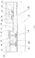
- a lower semiconductor layer is provided on the base substrate 101 .
- a buffer layer 102 is provided on the base substrate 101 by, such as, plasma enhanced chemical vapor deposition method (PECVD).
- the base substrate 101 may be of a transparent material possessing a good transmittance, such as, glass, hard transparent plastic, etc.; and the buffer layer 102 comprises a silicon oxide structural layer and a silicon nitride structural layer disposed sequentially, or comprises a composite layer of a silicon oxide structural layer and a silicon nitride structural layer.
- the thickness of the silicon oxide structural layer is in the range of 50 nm to 100 nm, and the thickness of the silicon nitride structural layer is in the range of 100 nm to 300 nm.
- a lower semiconductor layer is provided on the buffer layer 102 .
- an amorphous silicon thin film is provided on the buffer layer 102 by, such as, plasma enhanced chemical vapor deposition method.
- the thickness of the amorphous silicon thin film is in the range of 40 nm to 50 nm.
- the base substrate 101 is sent into a high-temperature reaction furnace, and a dehydrogenating treatment is conducted on the amorphous silicon thin film so as to reduce the hydrogen content in the amorphous silicon thin film.
- the content of hydrogen is controlled to be no more than 2%.
- the amorphous silicon thin film is subjected to such as an excimer laser annealing treatment, so that the amorphous silicon thin film is converted into a polycrystalline silicon thin film, which is the lower semiconductor layer.
- a plurality of P-type semiconductor active layers 103 are formed in the lower semiconductor layer by a masking/photolithography process; and a P-type semiconductor active layer 103 comprises a source contact region 104 , a drain contact region 105 and an active-layer linkage region 106 disposed between the source contact region 104 and the drain contact region 105 .
- the masking/photolithography process in embodiments of the invention may include photoresist coating, mask provision, exposure, development, etching, photoresist removing and other procedures.
- a gate insulating layer 107 is provided on the lower semiconductor layer.
- a gate insulating layer is provided on the lower semiconductor layer by plasma enhanced chemical vapor deposition method.
- the gate insulating layer 107 comprises a composite layer of a silicon oxide structural layer and a silicon nitride structural layer, and in another example, the thickness of the silicon oxide structural layer is in the range of 50 nm to 100 nm, and the thickness of the silicon nitride structural layer is in the range of 40 nm to 80 nm.
- the gate insulating layer 107 acts to separate the P-type semiconductor active layer 103 from a P-type transistor gate electrode, so that an electronic signal crosstalk will not occur between the two components in operation.
- a lower electrode layer is provided on the gate insulating layer 107 by such as magnetron sputtering process.
- a plurality of P-type transistor gate electrodes 108 , a plurality of N-type transistor source electrodes 109 and a plurality of N-type transistor drain electrodes 110 are formed on the lower electrode layer through a masking/photolithography process; and the P-type transistor gate electrodes 108 are located over the P-type semiconductor active layers 103 .
- the lower electrode layer is made of any of metals including molybdenum, tungsten, titanium or chromium.
- the P-type semiconductor active layers 103 are doped by, such as, ion implantation process. During the implantation, with P-type transistor gate electrodes 108 over active layer linkage regions 106 as a mask, a self-alignment process is realized. Dopants are implanted into the source contact region 104 and the drain contact region 105 , respectively, so as to form a source contact region 104 and a drain contact region 105 with dopants.
- Dopants in the source contact region 104 and the drain contact region 105 are highly activated by an activating process, so as to endow the activated dopants in an ionic state with a higher moving ability, and thus they are automatically filled to suitable locations in the source contact region 104 and the drain contact region 105 for repairing lattice defects within them.
- an upper semiconductor layer is provided above the lower electrode layer by using such as an oxide semiconductor material and by such as magnetron sputtering process.
- a pixel electrode 111 and an N-type semiconductor active layer 112 are formed of the upper semiconductor layer by such as patterning process.
- two ends of the N-type semiconductor active layer 112 overlap and contact the N-type transistor source electrode 109 and the N-type transistor drain electrode 110 , respectively.
- the oxide semiconductor material corresponding to the pixel electrode 111 region is subjected to, such as, plasma treatment.
- the plasma treatment process comprises that, in a vacuum chamber, the oxide semiconductor material corresponding to the pixel electrode 111 region is treated with O 2 plasma, N 2 O plasma or N 2 plasma; the power is in the range of 1500 W to 2500 W, the pressure is in the range of 1000 mtorr to 2000 mtorr, and the gas flow rate is in the range of 5000 sccm to 15000 sccm.
- the carrier density in the oxide semiconductor material can be enhanced so as to increase its conductivity.
- the upper semiconductor layer adopts one or more materials selected from the group consisting of indium gallium zinc oxide, zinc oxide, indium zinc oxide, indium tin zinc oxide and other transparent metal oxide semiconductor material.
- an isolation insulating protective layer 113 is provided on the upper semiconductor layer by such as plasma enhanced chemical vapor deposition process.
- the isolation insulating protective layer 113 comprises a composite layer of a silicon oxide structural layer and a silicon nitride structural layer.
- a protection unit 115 between an N-type transistor gate electrode and an N-type semiconductor active layer 112 and contact holes 114 located at both ends of a P-type semiconductor active layer 103 and in a region corresponding to the pixel electrode 111 are formed from the isolation insulating protective layer 113 by masking/photolithography process.
- the contact holes 114 penetrate the isolation insulating protective layer 113 up to the source contact region 104 and the drain contact region 105 of the P-type semiconductor active layer 103 .
- an upper electrode layer is provided on the isolation insulating protective layer 113 by such as magnetron sputtering process.
- the upper electrode layer is made of any of metals including aluminum, titanium or silver or an alloy consisting of several metals selected from them as desire.
- a P-type transistor source electrode 116 , a P-type transistor drain electrode 117 and an N-type transistor gate electrode 118 are formed on the upper electrode layer by masking/photolithography process.
- the P-type transistor source electrode 116 and the P-type transistor drain electrode 117 are connected to ends of a p-type semiconductor active layer 103 through contact holes 114 , and the P-type transistor drain electrode 117 is also connected to the pixel electrode 111 ; the N-type transistor gate electrode 118 is located over the N-type semiconductor active layer 112 .
- the P-type transistor comprises the P-type semiconductor active layer 103 , the P-type transistor gate electrode 108 , the P-type transistor source electrode 116 and the P-type transistor drain electrode 117 ; and the N-type transistor comprises the N-type semiconductor active layer 112 , the N-type transistor gate electrode 118 , the N-type transistor source electrode 109 and the N-type transistor drain electrode 110 .
- a pixel defining layer 119 is provided on the upper electrode layer by such as spin-coating process, and a pixel connection opening 120 is formed on the pixel defining layer by such as masking/photolithography process.
- the pixel connection opening 120 is disposed on the pixel electrode 11 between two adjacent protection units 115 . Up to here, the manufacture of the complementary thin film transistor drive back-plate is finished.
- the pixel connection opening 120 is used for the corresponding connection between an organic light emitting layer in an organic electroluminescent substrate and the pixel electrode, so as to achieve the luminous drive of the organic electroluminescent substrate by the complementary thin film transistor drive back-plate.
- the pixel electrode in the embodiment is just part of an anode layer in the organic electroluminescent substrate.
- an N-type transistor source electrode and a source contact region are integrated into one N-type transistor source electrode of a metallic substance, and accordingly, an N-type transistor drain electrode and a drain contact region, the material of which is a semiconductor material, are integrated into one N-type transistor drain electrode of a metallic substance.
- the N-type transistor source electrode 109 and the N-type transistor drain electrode 110 are connected by using an N-type semiconductor active layer 112 , replacing an active-layer linkage region of an N-type transistor; in this way, a step of doping a source contact region of an N-type transistor, a drain contact region of the N-type transistor and an N-type semiconductor active layer can be omitted.
- the process steps are effectively simplified, the fabricating cost is reduced, and the fabricating efficiency is improved.
- contact holes 114 and protection units 115 are formed in the same isolation insulating protective layer 113 in the same process, and the protection units 115 act as an interlayer dielectric layer on the P-type transistor gate electrode 108 and a gate insulating layer for the N-type transistor gate electrode 118 , respectively.
- the interlayer dielectric layer and the gate insulating layer are merged into a single-layer structure and can be formed by one masking/photolithography process, and this reduces the thickness of the complementary thin film transistor drive back-plate.
- the process steps are simplified, the fabricating cost is reduced, and the fabricating efficiency is improved.
- the P-type transistor source electrode 116 , the P-type transistor drain electrode 117 and the N-type transistor gate electrode 118 are formed on the same upper electrode layer, and this makes these three electrodes are formed of the same metallic material.
- a step of forming an N-type transistor gate electrode 118 separately by a masking/photolithography process can be omitted.
- the process steps are simplified, the fabricating cost is reduced, and the fabricating efficiency is improved.
- a complementary thin film transistor drive back-plate can be made by only six masking/photolithography processes. As compared with other manufacturing method, at least five masking/photolithography processes are saved, and the fabricating cost is reduced greatly; and meanwhile, the fabricated complementary thin film transistor drive back-plate become lighter and thinner.
- P-type transistor source electrodes P-type transistor drain electrodes
- N-type transistor source electrodes N-type transistor drain electrodes
- a P-type transistor source electrode may also be called as a P-type transistor drain electrode
- a P-type transistor drain electrode may also be called as a P-type transistor source electrode.
- a complementary thin film transistor drive back-plate in the embodiment is made by the manufacturing method in the first embodiment, and therefore, the technical contents disclosed in the first embodiment will not be described repetitively. Contents disclosed by the first embodiment also belong to the contents disclosed by the present embodiment.
- a complementary thin film transistor drive back-plate which is made by, such as the manufacturing method of the complementary thin film transistor drive back-plate stated in the first embodiment.
- the complementary thin film transistor drive back-plate in the embodiment comprises a base substrate 101 , and on the base substrate 101 and from bottom to top, there are sequentially provided a buffer layer 102 ; a lower semiconductor layer including a plurality of P-type semiconductor active layers 103 ; a gate insulating layer 107 ; a lower electrode layer including a plurality of P-type transistor gate electrodes 108 , a plurality of N-type transistor source electrodes 109 and a plurality of N-type transistor drain electrodes 110 ; an upper semiconductor layer including a plurality of pixel electrodes 111 and a plurality of N-type semiconductor active layers 112 ; an isolation insulating protective layer 113 including a plurality of contact holes 114 and a plurality of protection units 115 ; an upper electrode layer including a plurality of P-type transistor source electrodes 116 , a plurality of P-type transistor drain electrodes 117 and a plurality of N-type transistor gate electrodes 118 ; and a pixel defining layer 119
- a P-type semiconductor active layer 103 stated in the embodiment comprises a source contact region 104 , a drain contact region 105 and an active-layer linkage region 106 disposed between the source contact region 104 and the drain contact region 105 ; the P-type transistor gate electrodes 108 are disposed over the P-type semiconductor active layers 103 and correspond to locations of active-layer linkage regions 106 ; the gate insulating layer 107 is disposed between the P-type transistor gate electrodes 108 and the P-type semiconductor active layers 103 ; on the P-type transistor gate electrodes 108 , there are provided the protection units 115 , which fully encapsulate the P-type transistor gate electrodes 108 ; the upper part of a P-type transistor source electrode is arranged on a protection unit 115 , and the lower part thereof goes deeply into a contact hole 114 to connect a source contact region 104 ; the upper part of a P-type transistor drain electrode 117 is arranged on a protection unit 115 , and the lower part thereof goes deeply into
- the pixel electrode 111 stated in the embodiment is disposed on the gate insulating layer 107 between a P-type semiconductor active layer 103 and an N-type semiconductor active layer 112 ; an N-type transistor source electrode 109 and an N-type transistor drain electrode 110 are connected by an N-type semiconductor active layer 112 ; an N-type transistor gate electrode 118 is disposed over an N-type semiconductor active layer 112 and corresponds to location of the N-type semiconductor active layer 112 ; between an N-type transistor gate electrode 118 and an N-type semiconductor active layer 112 , there is provided a protection unit 115 , which fully encapsulates the N-type semiconductor active layer 112 together with an N-type transistor source electrode 116 and an N-type transistor drain electrode 117 ; the pixel defining layer 119 covers the N-type transistor gate electrodes 118 from the above as a whole, and fully encapsulates a protection unit 115 located between an N-type transistor gate electrode 118 and an N-type semiconductor active layer 112 .
- the upper part of a P-type transistor drain electrode 117 stated in the embodiment is connected to a pixel electrode 111 .
- a right end of a protection unit 115 located on a P-type transistor gate electrode 108 in the embodiment is placed on a left end of a pixel electrode; and as for a protection unit 115 located between an N-type transistor gate electrode 118 and an N-type semiconductor active layer 112 , the left end of the protection unit is placed on a right end of the pixel electrode.
- the pixel connection openings 120 in the embodiment penetrate the pixel defining layer 119 , and they are arranged on pixel electrodes 111 in correspondence.
- the drive back-plate in the embodiment adopts a design of arranging a pixel electrode 111 between two adjacent protection units 115 .
- the pixel electrode 111 can be reasonably placed in the space between a P-type transistor and an N-type transistor, without changing its own structural characteristics of the complementary thin film transistor drive back-plate.
- pixel electrodes 111 and P-type semiconductor active layers 103 can be formed simultaneously through the same one masking/photolithography process. As such, the step of forming pixel electrodes 111 separately through a masking/photolithography process is omitted, so that the overall thickness of the complementary thin film transistor drive back-plate can be reduced effectively.
- the process steps are effectively simplified, the fabricating cost is reduced, and the fabricating efficiency is improved.
- Each of the P-type transistor gate electrodes 108 , the N-type transistor source electrodes 109 and the N-type transistor drain electrodes 110 as stated in the embodiment is made of any of metals including molybdenum, tungsten, titanium or chromium, or an alloy of several metals selected from them as desire.
- Each of the pixel electrodes 111 , the N-type transistor source electrodes 109 and the N-type transistor drain electrodes 110 in the embodiment is made of any one selected from the group consisting of an indium gallium zinc oxide, a zinc oxide, a indium zinc oxide, a indium tin zinc oxide and other transparent metal oxide semiconductor material or a composite of several materials selected from them as desire.
- Each of the P-type transistor source electrodes 116 , the P-type transistor drain electrodes 117 and the N-type transistor gate electrodes 118 in the embodiment is made of any of metals including aluminum, titanium or silver or an alloy consisting of several metals selected from them as desire.
- a display panel in the embodiment comprises a complementary thin film transistor drive back-plate as stated in the second embodiment, and therefore, technical contents disclosed in the second embodiment will not be described repetitively. Contents disclosed by the second embodiment also belong to contents disclosed by the present embodiment.
- a display panel is provided by the present embodiment, and in an example, the display panel is an active matrix organic light emitting diode panel.
- the display panel comprises a complementary thin film transistor drive back-plate, such as that stated in the second embodiment, and an organic electroluminescent substrate disposed on the complementary thin film transistor drive back-plate.
- On the organic electroluminescent substrate for example, there are provided an anode layer, an organic luminous layer and a cathode layer from bottom to top.
- the organic luminous layer is mounted corresponding to a pixel electrode, so as to achieve the luminous drive of the organic electroluminescent substrate by the complementary thin film transistor drive back-plate.
- the pixel electrode stated in the embodiment is just a part of the anode layer in the organic electroluminescent substrate.
Landscapes
- Thin Film Transistor (AREA)
- Devices For Indicating Variable Information By Combining Individual Elements (AREA)
- Electroluminescent Light Sources (AREA)
- Metal-Oxide And Bipolar Metal-Oxide Semiconductor Integrated Circuits (AREA)
Abstract
Description
-
- 1. in embodiments of the invention, the P-type transistor gate electrodes, the N-type transistor source electrodes and the N-type transistor drain electrodes of the same metallic substance are formed by a same lower electrode layer, and the pixel electrodes and the N-type semiconductor active layers are formed by a same upper semiconductor layer. In this way, an N-type transistor source electrode and a source contact region, the material of which is a semiconductor material, are merged into one N-type transistor source electrode of a metallic substance, and accordingly, an N-type transistor drain electrode and a drain contact region, the material of which is a semiconductor material, are merged into one N-type transistor drain electrode of a metallic substance. According to embodiments of the invention, an N-type transistor source electrode and an N-type transistor drain electrode are connected by using an N-type semiconductor active layer, replacing an active-layer linkage region of an N-type transistor. With this structure, a step of doping a source contact region of an N-type transistor, a drain contact region of the N-type transistor and an N-type semiconductor active layer is omitted. Thus, according to embodiments of the invention, the process steps are effectively simplified, the fabricating cost is reduced, and the fabricating efficiency is improved.
- 2. In embodiments of the invention, contact holes and protection units that act as an interlayer dielectric layer on a P-type transistor gate electrode and a gate insulating layer for the N-type transistor gate electrode, respectively, are formed in the same isolation insulating protective layer. As such, the interlayer dielectric layer and the gate insulating layer are merged into a single layer structure and can be formed by one masking/photolithography process. Thus, according to embodiments of the invention, the thickness of the complementary thin film transistor drive back-plate is reduced; and furthermore, the process steps are simplified, the fabricating cost is reduced, and the fabricating efficiency is improved.
- 3. In embodiments of the invention, P-type transistor source electrodes, P-type transistor drain electrodes and N-type transistor gate electrodes are formed by a same upper electrode layer, and this makes these three layer formed of a same metallic material. Thereby, a step of forming N-type transistor gate electrodes separately by a masking/photolithography process can be omitted. Thus, according to embodiments of the invention, the process steps are simplified, the fabricating cost is reduced, and the fabricating efficiency is improved.
- 4. Embodiments of the invention adopt a design of arranging a pixel electrode between two adjacent protection units. With this design, the pixel electrode is placed in the space between a P-type transistor and an N-type transistor, without changing its own structural characteristics of the complementary thin film transistor drive back-plate. Furthermore, pixel electrodes and P-type semiconductor active layers are formed simultaneously through one masking/photolithography process. As such, a step of forming pixel electrodes separately through a masking/photolithography process is omitted, and the overall thickness of the complementary thin film transistor drive back-plate can be reduced effectively. Thus, according to embodiments of the invention, the process steps are effectively simplified, the fabricating cost is reduced, and the fabricating efficiency is improved.
Claims (6)
Applications Claiming Priority (4)
| Application Number | Priority Date | Filing Date | Title |
|---|---|---|---|
| CN201310742725 | 2013-12-27 | ||
| CN201310742725.3 | 2013-12-27 | ||
| CN201310742725.3A CN103715147B (en) | 2013-12-27 | 2013-12-27 | Complementary thin-film transistor drives backboard and preparation method thereof, display floater |
| PCT/CN2014/081190 WO2015096441A1 (en) | 2013-12-27 | 2014-06-30 | Complementary-type thin film transistor driving backplate, manufacturing method therefor, and display device |
Publications (2)
| Publication Number | Publication Date |
|---|---|
| US20160013212A1 US20160013212A1 (en) | 2016-01-14 |
| US10804300B2 true US10804300B2 (en) | 2020-10-13 |
Family
ID=50408010
Family Applications (1)
| Application Number | Title | Priority Date | Filing Date |
|---|---|---|---|
| US14/428,832 Active 2035-02-15 US10804300B2 (en) | 2013-12-27 | 2014-06-30 | Complementary thin film transistor drive back-plate and manufacturing method thereof, display panel |
Country Status (3)
| Country | Link |
|---|---|
| US (1) | US10804300B2 (en) |
| CN (1) | CN103715147B (en) |
| WO (1) | WO2015096441A1 (en) |
Families Citing this family (15)
| Publication number | Priority date | Publication date | Assignee | Title |
|---|---|---|---|---|
| CN103579115B (en) | 2013-11-11 | 2015-11-25 | 京东方科技集团股份有限公司 | Complementary thin-film transistor and preparation method thereof, array base palte, display unit |
| CN103715147B (en) * | 2013-12-27 | 2016-08-17 | 京东方科技集团股份有限公司 | Complementary thin-film transistor drives backboard and preparation method thereof, display floater |
| US10020354B2 (en) * | 2015-04-17 | 2018-07-10 | Apple Inc. | Organic light-emitting diode displays with silicon and semiconducting oxide thin-film transistors |
| CN105575992A (en) * | 2015-12-22 | 2016-05-11 | 深圳市华星光电技术有限公司 | Complementary metal oxide semiconductor and preparation method |
| JP6740015B2 (en) * | 2016-06-10 | 2020-08-12 | 株式会社ジャパンディスプレイ | Semiconductor device and method of manufacturing semiconductor device |
| CN106328592A (en) * | 2016-10-27 | 2017-01-11 | 京东方科技集团股份有限公司 | Thin film transistor and manufacturing method, the array substrate and display device |
| KR102603300B1 (en) * | 2016-12-30 | 2023-11-15 | 엘지디스플레이 주식회사 | Thin film transistor, method for manufacturing the same, and organic light emitting display device including the same |
| WO2019014901A1 (en) * | 2017-07-20 | 2019-01-24 | 华为技术有限公司 | Field effect transistor and manufacturing method |
| CN107527941B (en) * | 2017-08-31 | 2019-09-17 | 维信诺科技股份有限公司 | A kind of organic light emitting display and its manufacturing method |
| CN110718467B (en) * | 2019-09-24 | 2021-12-03 | Tcl华星光电技术有限公司 | Manufacturing method of TFT array substrate |
| CN110648629B (en) * | 2019-10-31 | 2023-09-22 | 厦门天马微电子有限公司 | Display panel, manufacturing method and display device thereof |
| CN110827758A (en) * | 2019-10-31 | 2020-02-21 | 福建华佳彩有限公司 | Layered AMOLED pixel compensation circuit |
| CN114005848B (en) * | 2020-07-28 | 2024-09-03 | 合肥鑫晟光电科技有限公司 | A driving backplane, a manufacturing method thereof, a backlight module and a display device |
| CN115377120A (en) * | 2022-08-09 | 2022-11-22 | 武汉华星光电技术有限公司 | Vertical inverter and semiconductor device |
| US12289907B2 (en) | 2022-08-09 | 2025-04-29 | Wuhan China Star Optoelectronics Technology Co., Ltd. | Vertical inverter and semiconductor device |
Citations (8)
| Publication number | Priority date | Publication date | Assignee | Title |
|---|---|---|---|---|
| CN1708860A (en) | 2002-10-30 | 2005-12-14 | 先锋株式会社 | Organic semiconductor device |
| US20060220542A1 (en) * | 2005-03-30 | 2006-10-05 | Suh Min-Chul | Flat panel display and method of manufacturing the same |
| CN101064345A (en) | 2006-04-27 | 2007-10-31 | 三星电子株式会社 | Thin film transistor and method of fabricating the same |
| US20110049523A1 (en) | 2009-08-25 | 2011-03-03 | Jong-Hyun Choi | Organic light emitting diode display and method of manufacturing the same |
| US20130207087A1 (en) * | 2012-02-09 | 2013-08-15 | Lg Display Co., Ltd. | Organic light emitting display device and method for fabricating the same |
| WO2013183495A1 (en) | 2012-06-08 | 2013-12-12 | シャープ株式会社 | Semiconductor device and method for manufacturing same |
| CN103715147A (en) | 2013-12-27 | 2014-04-09 | 京东方科技集团股份有限公司 | Complementary type thin film transistor drive backboard, manufacturing method thereof and display panel |
| US20150123084A1 (en) * | 2013-11-05 | 2015-05-07 | Samsung Display Co., Ltd. | Thin film transistor array substrate, organic light-emitting display apparatus and method of manufacturing the thin film transistor array substrate |
-
2013
- 2013-12-27 CN CN201310742725.3A patent/CN103715147B/en active Active
-
2014
- 2014-06-30 WO PCT/CN2014/081190 patent/WO2015096441A1/en not_active Ceased
- 2014-06-30 US US14/428,832 patent/US10804300B2/en active Active
Patent Citations (12)
| Publication number | Priority date | Publication date | Assignee | Title |
|---|---|---|---|---|
| CN1708860A (en) | 2002-10-30 | 2005-12-14 | 先锋株式会社 | Organic semiconductor device |
| US7342245B2 (en) | 2002-10-30 | 2008-03-11 | Pioneer Corporation | Organic semiconductor device |
| US20060220542A1 (en) * | 2005-03-30 | 2006-10-05 | Suh Min-Chul | Flat panel display and method of manufacturing the same |
| CN101064345A (en) | 2006-04-27 | 2007-10-31 | 三星电子株式会社 | Thin film transistor and method of fabricating the same |
| US20070252207A1 (en) | 2006-04-27 | 2007-11-01 | Samsung Electronics Co. Ltd. | Thin film transistor and method of fabricating the same |
| US20110049523A1 (en) | 2009-08-25 | 2011-03-03 | Jong-Hyun Choi | Organic light emitting diode display and method of manufacturing the same |
| CN101997025A (en) | 2009-08-25 | 2011-03-30 | 三星移动显示器株式会社 | Organic light emitting diode display and method of manufacturing the same |
| US8455876B2 (en) | 2009-08-25 | 2013-06-04 | Samsung Display Co., Ltd. | Organic light emitting diode display and method of manufacturing the same |
| US20130207087A1 (en) * | 2012-02-09 | 2013-08-15 | Lg Display Co., Ltd. | Organic light emitting display device and method for fabricating the same |
| WO2013183495A1 (en) | 2012-06-08 | 2013-12-12 | シャープ株式会社 | Semiconductor device and method for manufacturing same |
| US20150123084A1 (en) * | 2013-11-05 | 2015-05-07 | Samsung Display Co., Ltd. | Thin film transistor array substrate, organic light-emitting display apparatus and method of manufacturing the thin film transistor array substrate |
| CN103715147A (en) | 2013-12-27 | 2014-04-09 | 京东方科技集团股份有限公司 | Complementary type thin film transistor drive backboard, manufacturing method thereof and display panel |
Non-Patent Citations (3)
| Title |
|---|
| Chinese Office Action of Chinese Application No. 201310742725.3, dated Sep. 24, 2015 with English translation. |
| International Search Report with Notice of Transmittal of the International Search Report of PCT/CN2014/081190 in Chinese, dated Oct. 10, 2014. |
| Written Opinion of the International Searching Authority of PCT/CN2014/081190 in Chinese with English translation dated Oct. 10, 2014. |
Also Published As
| Publication number | Publication date |
|---|---|
| WO2015096441A1 (en) | 2015-07-02 |
| CN103715147A (en) | 2014-04-09 |
| CN103715147B (en) | 2016-08-17 |
| US20160013212A1 (en) | 2016-01-14 |
Similar Documents
| Publication | Publication Date | Title |
|---|---|---|
| US10804300B2 (en) | Complementary thin film transistor drive back-plate and manufacturing method thereof, display panel | |
| JP7058724B2 (en) | TFT substrate and its manufacturing method, and OLED panel manufacturing method | |
| CN101997025B (en) | Organic light emitting diode display and method of manufacturing the same | |
| CN104253159B (en) | Thin film transistor (TFT) and preparation method, array base palte and preparation method and display device | |
| US10325938B2 (en) | TFT array substrate, method for manufacturing the same, and display device | |
| CN102646699B (en) | Oxide TFT (thin film transistor) and manufacturing method thereof | |
| KR101158896B1 (en) | Substrate having thin film transistor and method for making the substrate, and liquid crystal display panel and electro luminescence display panel having the transistor | |
| US9543415B2 (en) | Thin film transistor driving backplane and manufacturing method thereof, and display panel | |
| US10658446B2 (en) | Method for manufacturing OLED backplane comprising active layer formed of first, second, and third oxide semiconductor layers | |
| CN104218041B (en) | Array base palte and preparation method and display device | |
| EP2747141A1 (en) | Thin film transisitor and manufacturing method thereof, array substrate, and display device | |
| US10096663B2 (en) | Manufacturing method of array substrate, array substrate and display device | |
| US20160254287A1 (en) | Thin-Film Transistor, Manufacturing Method Thereof, Display Substrate and Display Device | |
| US11217698B2 (en) | Method of manufacturing a thin film transistor | |
| US9048458B2 (en) | Method of fabricating pixel structure for organic light-emitting display | |
| CN111613664A (en) | Thin film transistor, method for producing the same, and display panel | |
| CN105655407A (en) | Polycrystalline silicon thin film transistor and preparation method thereof, array substrate and display device | |
| CN110197851A (en) | Thin film transistor (TFT) and its manufacturing method, array substrate and electronic device | |
| KR100934480B1 (en) | Organic light emitting display panel and manufacturing method thereof | |
| CN114203732A (en) | LTPO substrate, manufacturing method thereof and display panel | |
| WO2016078297A1 (en) | Pixel structure and manufacturing method therefor, array substrate, and display device | |
| WO2018192009A1 (en) | Method for use in fabricating low-temperature polysilicon thin film transistor | |
| KR20140083150A (en) | Organic electro luminescent device and method of fabricating the same | |
| CN103247571B (en) | Manufacturing method of pixel structure for organic light emitting display | |
| CN203445123U (en) | Thin-film transistor drive backplane and display panel |
Legal Events
| Date | Code | Title | Description |
|---|---|---|---|
| AS | Assignment |
Owner name: BOE TECHNOLOGY GROUP CO., LTD., CHINA Free format text: ASSIGNMENT OF ASSIGNORS INTEREST;ASSIGNOR:IM, JANG SOON;REEL/FRAME:035183/0518 Effective date: 20150125 |
|
| STPP | Information on status: patent application and granting procedure in general |
Free format text: DOCKETED NEW CASE - READY FOR EXAMINATION |
|
| STPP | Information on status: patent application and granting procedure in general |
Free format text: NON FINAL ACTION MAILED |
|
| STPP | Information on status: patent application and granting procedure in general |
Free format text: RESPONSE TO NON-FINAL OFFICE ACTION ENTERED AND FORWARDED TO EXAMINER |
|
| STPP | Information on status: patent application and granting procedure in general |
Free format text: FINAL REJECTION MAILED |
|
| STPP | Information on status: patent application and granting procedure in general |
Free format text: DOCKETED NEW CASE - READY FOR EXAMINATION |
|
| STPP | Information on status: patent application and granting procedure in general |
Free format text: NOTICE OF ALLOWANCE MAILED -- APPLICATION RECEIVED IN OFFICE OF PUBLICATIONS |
|
| STPP | Information on status: patent application and granting procedure in general |
Free format text: PUBLICATIONS -- ISSUE FEE PAYMENT VERIFIED |
|
| STCF | Information on status: patent grant |
Free format text: PATENTED CASE |
|
| MAFP | Maintenance fee payment |
Free format text: PAYMENT OF MAINTENANCE FEE, 4TH YEAR, LARGE ENTITY (ORIGINAL EVENT CODE: M1551); ENTITY STATUS OF PATENT OWNER: LARGE ENTITY Year of fee payment: 4 |