US10798323B1 - Control method for an active pixel image sensor - Google Patents
Control method for an active pixel image sensor Download PDFInfo
- Publication number
- US10798323B1 US10798323B1 US16/070,885 US201716070885A US10798323B1 US 10798323 B1 US10798323 B1 US 10798323B1 US 201716070885 A US201716070885 A US 201716070885A US 10798323 B1 US10798323 B1 US 10798323B1
- Authority
- US
- United States
- Prior art keywords
- node
- memory node
- pixels
- readout
- integration period
- Prior art date
- Legal status (The legal status is an assumption and is not a legal conclusion. Google has not performed a legal analysis and makes no representation as to the accuracy of the status listed.)
- Active, expires
Links
- 238000000034 method Methods 0.000 title claims description 37
- 230000010354 integration Effects 0.000 claims abstract description 94
- 238000005070 sampling Methods 0.000 claims abstract description 26
- 230000002596 correlated effect Effects 0.000 claims abstract description 12
- 238000012163 sequencing technique Methods 0.000 claims description 23
- 230000000875 corresponding effect Effects 0.000 claims description 22
- 238000005259 measurement Methods 0.000 claims description 10
- 230000001276 controlling effect Effects 0.000 claims description 7
- 238000005036 potential barrier Methods 0.000 claims description 7
- 230000035945 sensitivity Effects 0.000 abstract description 6
- 230000004907 flux Effects 0.000 description 14
- 239000004020 conductor Substances 0.000 description 11
- 238000005516 engineering process Methods 0.000 description 10
- 230000004044 response Effects 0.000 description 10
- 238000010586 diagram Methods 0.000 description 9
- 238000005286 illumination Methods 0.000 description 9
- 239000004065 semiconductor Substances 0.000 description 9
- 238000003860 storage Methods 0.000 description 8
- 239000000758 substrate Substances 0.000 description 6
- 230000006870 function Effects 0.000 description 5
- 238000009792 diffusion process Methods 0.000 description 4
- 230000000694 effects Effects 0.000 description 4
- 239000011159 matrix material Substances 0.000 description 4
- 108010075750 P-Type Calcium Channels Proteins 0.000 description 3
- 229920006395 saturated elastomer Polymers 0.000 description 3
- 108091006146 Channels Proteins 0.000 description 2
- 230000004888 barrier function Effects 0.000 description 2
- 230000008859 change Effects 0.000 description 2
- 239000002019 doping agent Substances 0.000 description 2
- 238000009825 accumulation Methods 0.000 description 1
- 230000003213 activating effect Effects 0.000 description 1
- 230000006978 adaptation Effects 0.000 description 1
- 239000003990 capacitor Substances 0.000 description 1
- 238000006243 chemical reaction Methods 0.000 description 1
- 230000003247 decreasing effect Effects 0.000 description 1
- 239000006185 dispersion Substances 0.000 description 1
- 230000006872 improvement Effects 0.000 description 1
- 238000012432 intermediate storage Methods 0.000 description 1
- 230000001105 regulatory effect Effects 0.000 description 1
- 238000005096 rolling process Methods 0.000 description 1
- 238000009738 saturating Methods 0.000 description 1
Images


Classifications
-
- H04N5/35554—
-
- H—ELECTRICITY
- H04—ELECTRIC COMMUNICATION TECHNIQUE
- H04N—PICTORIAL COMMUNICATION, e.g. TELEVISION
- H04N25/00—Circuitry of solid-state image sensors [SSIS]; Control thereof
- H04N25/50—Control of the SSIS exposure
- H04N25/57—Control of the dynamic range
- H04N25/571—Control of the dynamic range involving a non-linear response
- H04N25/575—Control of the dynamic range involving a non-linear response with a response composed of multiple slopes
-
- H—ELECTRICITY
- H04—ELECTRIC COMMUNICATION TECHNIQUE
- H04N—PICTORIAL COMMUNICATION, e.g. TELEVISION
- H04N25/00—Circuitry of solid-state image sensors [SSIS]; Control thereof
- H04N25/50—Control of the SSIS exposure
- H04N25/57—Control of the dynamic range
- H04N25/58—Control of the dynamic range involving two or more exposures
- H04N25/581—Control of the dynamic range involving two or more exposures acquired simultaneously
- H04N25/583—Control of the dynamic range involving two or more exposures acquired simultaneously with different integration times
-
- H—ELECTRICITY
- H04—ELECTRIC COMMUNICATION TECHNIQUE
- H04N—PICTORIAL COMMUNICATION, e.g. TELEVISION
- H04N25/00—Circuitry of solid-state image sensors [SSIS]; Control thereof
- H04N25/50—Control of the SSIS exposure
- H04N25/57—Control of the dynamic range
- H04N25/58—Control of the dynamic range involving two or more exposures
- H04N25/587—Control of the dynamic range involving two or more exposures acquired sequentially, e.g. using the combination of odd and even image fields
- H04N25/589—Control of the dynamic range involving two or more exposures acquired sequentially, e.g. using the combination of odd and even image fields with different integration times, e.g. short and long exposures
-
- H—ELECTRICITY
- H04—ELECTRIC COMMUNICATION TECHNIQUE
- H04N—PICTORIAL COMMUNICATION, e.g. TELEVISION
- H04N25/00—Circuitry of solid-state image sensors [SSIS]; Control thereof
- H04N25/70—SSIS architectures; Circuits associated therewith
- H04N25/76—Addressed sensors, e.g. MOS or CMOS sensors
- H04N25/77—Pixel circuitry, e.g. memories, A/D converters, pixel amplifiers, shared circuits or shared components
- H04N25/771—Pixel circuitry, e.g. memories, A/D converters, pixel amplifiers, shared circuits or shared components comprising storage means other than floating diffusion
-
- H04N5/35527—
-
- H04N5/35581—
-
- H04N5/37452—
Definitions
- the invention relates to electronic image sensors operating on the basis of active pixels using MOS technology. More precisely, the invention relates to a method for controlling the various transistors which make up the active pixel.
- Active pixels most often comprise a photodiode that converts received photons to electric charge, and multiple MOS transistors allowing the readout of this charge and its conversion to electrical voltage to be controlled.
- a matrix-array sensor the rows of pixels are addressed individually and the voltages output by the pixels are applied to column conductors common to the pixels of a given column.
- Readout circuits at the foot of the column allow the voltages present on the columns to be sampled for each addressed row of pixels. The samples are stored in capacitors of the readout circuit. The samples are then converted to digital form by an analogue-to-digital converter (for example one converter for each column of pixels).
- Active pixels using a photodiode generally comprise at least four transistors: a transfer transistor that serves to transfer the charge from the photodiode to what is referred to as a readout node, which is a capacitive charge storage node; a readout transistor, which is connected in a voltage follower configuration and the gate of which is connected to the readout node in order to bring its source to a voltage representing the voltage of this node; a row-selection transistor controlled by a row conductor for selecting an entire row of pixels, this selection transistor allowing the output of the follower transistor of the pixel to be connected to the corresponding column conductor and thereby to the readout circuit at the foot of the column; and a reset transistor allowing the potential of the readout node to be reset to a reference value.
- a transfer transistor that serves to transfer the charge from the photodiode to what is referred to as a readout node, which is a capacitive charge storage node
- a readout transistor which is connected in a voltage
- the pixel control sequence in the common integration phase is the following:
- the phase of reading out the pixels may start.
- the pixels are read out sequentially, row by row.
- the selection transistor of the pixel is turned on for the time of a selection control pulse, and during this time:
- the readout circuit delivers as output, for each pixel, a measurement of the difference between the signal level and the reference level of the pixel.
- this level is not a precise measurement of the amount of charge generated in the photodiode because the random noise, referred to as kTC noise, is not removed.
- this noise is generated by the reset of the readout node by the reset transistor and means that the potential applied to the readout node is not absolutely certain.
- it is necessary first to be able to initialize the readout node in order to sample the reference potential level, and only after having established the (transfer) signal level in order to sample it. This is referred to as correlated double sampling (CDS) readout.
- CDS readout is not known to be possible when a common integration sequence is performed on all of the pixels at the same time.
- the memory node makes it possible to store the charge generated by the photodiode after each of the integration periods common to all the pixels, for the time it takes, in each row of pixels, to initialize the readout node of each of the pixels, and to sample the corresponding reference level in the readout circuit of each of the pixels of the row, then to transfer the charge from the memory node to the readout node and to sample the signal level in the readout circuit.
- the corresponding active pixel structure then comprises two transfer transistors (or gates), a first between the photodiode and the memory node and a second between the memory node and the readout node.
- the first transfer transistor between the photodiode and the memory node is then the transistor that controls the end of each integration period for all of the pixels at the same time, this end coinciding with the end of the transfer control pulse in the memory node.
- the second transfer transistor is employed in the sequential pixel row readout phase.
- One proposed solution consists of successively capturing multiple images with different integration times and, for each pixel, determining the best adapted signal from among the signals obtained. However, this increases the overall acquisition and processing time.
- Another solution consists of determining the time taken for a pixel to be saturated in order to deduce information on the light level therefrom in the case of saturating illumination. This assumes the presence of pixels of more complex structure and associated processing.
- Another solution uses the initialization transistor of the photodiodes during the integration period in order to allow excess charge to be removed from the photodiode by biasing the gate of this transistor to a set voltage below the threshold voltage of the transistor, in order to adjust the potential of the barrier of the semiconductor region under the gate. The response of the pixel then becomes logarithmic beyond a certain luminosity threshold.
- this solution is sensitive to technological dispersions (threshold voltages of the transistors, open circuit potential of the photodiodes).
- the invention proposes another method which allows the dynamic range of the sensor to be extended without modifying the structure or the size of the pixels. More specifically, it is envisaged to carry out, in the integration period common to the pixels, at least one transfer of charge from the photodiode to the memory node via the first transfer transistor, with an operation of clipping the amount of charge contained in the memory node in comparison with a threshold set by the second transfer transistor, allowing a change in the slope of the response curve beyond an intensity of luminous flux corresponding to this charge clipping threshold.
- the invention relates to a method for controlling an active pixel in an image sensor, the active pixel structure comprising a photosensitive element, a readout node and a memory node between the photosensitive element and the readout node, a first charge transfer transistor between the photosensitive element and the memory node and a second charge transfer transistor between the memory node and the readout node, a follower transistor, the gate of which is connected to the readout node, and at least one initialization transistor of the readout node.
- control method comprises the following steps, applied to all of the pixels simultaneously:
- the method comprises the application of N first and second pulses per integration period, N being an integer at least equal to 1, and the N first voltage pulses applied during an integration period divide said integration period into N+1 successive integration durations of increasingly shorter length, and the N second associated voltage pulses define N clipping thresholds in the memory node which keep increasing over the integration period.
- N is advantageously chosen to be equal to 2. Otherwise, N is set according to a measurement of the ambient light, preferably at a value chosen from between 1 and 2.
- the time of application of each first pulse and/or the clipping threshold associated with each second pulse are determined according to a measurement of the ambient light.
- the method advantageously applies a correlated double sampling for each pixel, with a first sampling of a reference level, corresponding to an initialization of the readout node, then a second sampling of a signal level corresponding to the charge which is contained in the memory node at the end of the integration period and which has been transferred to said readout node for readout.
- the invention also relates to an image sensor comprising at least one row of active pixels, with a pixel structure comprising a memory node between a photosensitive element and a readout node of the pixel, with a first charge transfer transistor placed between the photosensitive element and the memory node and a second charge transfer transistor placed between the memory node and the readout node, and a sequencing circuit for sequencing the signals required for image capture comprising an integration period common to all of the pixels, and a phase of successively reading out the pixels of each row, and the sequencing circuit is configured to implement such a control method.
- FIG. 1 illustrates a general structure of an active pixel to which the invention may be applied
- FIG. 2 is a timing diagram of the control signals for controlling a pixel in an image capture cycle, in a first exemplary implementation of the invention carrying out one (1) transfer/clipping operation per cycle;
- FIGS. 3 a to 3 h show, for each of phases 1 to 8 of the integration period of the cycle, the diagrams of the corresponding potentials in the structure of the pixel;
- FIG. 4 the corresponding response curve of a pixel, showing the amount of charge at the readout node as a function of the luminous flux
- FIGS. 5 a to 5 c show, for each of phases 9 to 11 of the CDS readout sequence of a pixel, the diagrams of the corresponding potentials in the structure of the pixel;
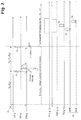
- FIGS. 6 and 7 show the signal timing diagram and the corresponding response curve for the pixel, for another exemplary implementation carrying out two transfer/clipping operations per image capture cycle.
- the invention pertains to an image capture method by an active pixel image sensor, with a pixel structure that comprises a memory node between the photodiode and the readout node. It is also necessary to provide a detailed description of such a structure, in order to facilitate the subsequent description of the method of the invention.
- Active pixels are produced using CMOS technology in a doped (for example p-doped) active semiconductor layer and in addition comprise photodiodes, which are in principle what are referred to as pinned photodiodes, capacitive storage nodes and transistors.
- Embodiments thereof employ various CMOS technologies well known to those skilled in the art.
- the context is that of a substrate with a p-doped active semiconductor layer, which substrate is biased to a zero reference potential and the circuits of which are supplied with a positive supply voltage denoted by Vdd.
- the various transistors of the pixels are NMOS transistors, with source and drain regions that are n-type diffusions on either side of a p-type channel under the gate.
- CMOS technology for example p-doped
- FIG. 1 is a circuit diagram of an exemplary structure of an active pixel with a memory node between a photosensitive element and a readout node: the pixel PIX comprises a photodiode Dp, a memory node MN which is a capacitive storage node, a readout node SN which is also a capacitive storage node, and a first transfer transistor TR 1 between the photodiode Dp and the memory node MN and a second transfer transistor TR 2 between the memory node MN and the readout node SN.
- the pixel PIX comprises a photodiode Dp, a memory node MN which is a capacitive storage node, a readout node SN which is also a capacitive storage node, and a first transfer transistor TR 1 between the photodiode Dp and the memory node MN and a second transfer transistor TR 2 between the memory node MN and the readout node SN.
- the pixel also comprises, in a conventional manner, a reset transistor RST for resetting the readout node SN, the source of which is electrically connected to the readout node and the drain of which is connected to the positive supply voltage Vdd; a follower transistor SF, the gate of which is electrically connected to the readout node SN, and the drain of which is biased to the supply voltage Vdd.
- a reset transistor RST for resetting the readout node SN, the source of which is electrically connected to the readout node and the drain of which is connected to the positive supply voltage Vdd
- a follower transistor SF the gate of which is electrically connected to the readout node SN, and the drain of which is biased to the supply voltage Vdd.
- the pixel comprises a selection transistor SEL, the gate of which is connected to a row conductor CL allowing the row of the pixel to be selected, the drain of which is electrically connected to the source of the follower transistor and the source of which is connected to a column conductor CC of the matrix array (the pixels being arranged in the form of a matrix, in n rows of rank j equal to 1 to n, and m columns of rank k equal to 1 to m), each column conductor CC being connected, at the foot of the column, to a readout circuit CR common to all of the pixels of the column.
- SEL selection transistor
- a sixth transistor AB is also provided, which allows the photodiode to be initialized, by removing charge via its drain.
- the photodiodes are initialized by activating (i.e. turning on), together in each pixel, the transistors TR 1 , TR 2 and RST.
- the transistors are not all necessarily constructed in a conventional manner, independently of the other elements of the pixel, with a source region, a drain region, a channel region separating the source from the drain and an insulated gate above the channel, as shown in FIG. 1 .
- Certain transistors are, in reality, essentially composed of an insulated gate to which a control potential may be applied.
- the first transfer transistor TR 1 may be composed of a simple transfer gate TR 1 - g , insulated from the substrate, surmounting a p-type channel region which is located between the n-type region of the photodiode Dp (source of TR 1 ) and the n-type region of the memory node MN (drain of TR 1 ).
- the second transfer transistor TR 2 may be composed of a simple transfer gate TR 2 - g , insulated from the substrate, surmounting a p-type channel region which is located between the n-type region of the memory node MN (source of TR 2 ) and the n-type region of the readout node SN (drain of TR 2 ).
- the source of the initialization transistor AB may be the n-type region of the photodiode which accumulates the charge generated by the light; and the source of the RST transistor may be the n-type region of the readout node.
- the term “gate” may be used to refer to these transistors.
- the selection transistor SEL, the follower transistor SF and/or the initialization transistor AB of the photodiodes may be common to a plurality or all of the pixels.
- the initialization transistor AB may be omitted, as stated above.
- the selection transistor may also not be present, the selection function then being provided by the reset transistor, via a drain bias voltage command capable of turning the follower transistor off outside of readout phases. In this case, the source of the follower transistor is directly connected to the column conductor. All of these structural variants of active pixels are known to those skilled in the art. The invention that will be described in relation to the structure of FIG. 1 is also applicable to these various variants.
- the photodiode Dp of the pixels is typically a pinned photodiode pinned to a voltage denoted by Vpin defined by the technology, i.e. it comprises, on the n-type diffusion region, a superficial p-type diffusion region and the superficial region is brought to the reference potential (zero) of the substrate.
- Vpin a voltage denoted by the technology, i.e. it comprises, on the n-type diffusion region, a superficial p-type diffusion region and the superficial region is brought to the reference potential (zero) of the substrate.
- the storage capacity of the photodiode is defined by its area.
- the readout node SN is generally composed of a floating n-doped semiconductor region.
- the charge storage capacity of this readout node is determined by its dopant concentration and its geometry.
- the memory node must be produced in a manner different from the floating diffusion of the readout node, since it must be possible to set its potential so as to allow it to be used as an intermediate storage node for storing the charge of the photodiode at the end of the integration period, for the time to allow the prior sampling in each pixel, in the readout phase, of the reference potential level of the readout node.
- its storage capacity must be equivalent to that of the readout node.
- the readout node is produced by a semiconductor region surmounted by a gate, and this gate is biased to a potential which allows the semiconductor region of the memory node to be set up under the gate at a determined potential level that is intermediate between the Vpin level of the photodiode and Vdd: it is thus possible to transfer the charge from the photodiode to the memory node at the end of the integration period; and, subsequently, to transfer the charge contained in the memory node to the readout node, in the readout phase.
- the applied potential may vary according to the phase in question, but, in order to simplify the following description, the potential of the memory node MN will hereinafter be considered to be a determined fixed value V MN .
- the charge storage capacity of the memory node depends, in this example, on the gate capacity (hence on its geometry), on the dopant concentration, etc.
- a pixel structure such as that which has been described is specially adapted to an image capture method in which an image capture cycle comprises one integration period common to all of the pixels, followed by a row-by-row readout of the pixels, i.e. a correlated double sampling readout (CDS readout). It is specified that the pixels are usually arranged in a matrix of rows and columns of pixels.
- CDS readout correlated double sampling readout
- the photodiode starts to accumulate charge again following the first transfer.
- this new charge is transferred to the memory node, and it is added to that already contained in the memory node following the one or more transfers and clipping operations carried out in the integration period.
- the transfer of charge to the memory node at an intermediate voltage is controlled through the application of a first voltage pulse to the first transfer gate.
- the clipping of the charge contained in the memory node is achieved through the application, after this first pulse, of a second voltage pulse to the second transfer gate, and the voltage of this pulse is at a determined level which sets the clipping threshold, i.e. the maximum amount of charge that can be held in the memory node, by setting the height of the potential barrier of the semiconductor region under the gate of the second transfer transistors in relation to the potential of the memory node.
- An initial state (not shown) is started from, in which the transfer transistors are in the off state.
- the initialization transistor of the readout node will generally be on (gate at Vdd), connecting the readout node SN to the supply voltage Vdd.
- the integration cycle starts with a phase ⁇ circle around (1) ⁇ of initializing all of the photodiodes.
- a voltage pulse Pi is applied to the initialization gate AB-g of the photodiodes ( FIGS. 2 and 3 a ) which turns the initialization transistors AB fully on so as to empty the photodiodes of all charge, via their drains D AB .
- the end of the initialization pulse Pi turns these transistors AB off again and sets the voltage t 0 of the start of the integration period common to the pixels of a new image capture cycle ( FIG. 3 b ).
- This pulse allows the charge accumulated by the photodiode since the end of the first transfer pulse to be transferred to the memory node MN: this charge is added to that held in the memory node following the transfer and clipping phases ⁇ circle around (2) ⁇ and ⁇ circle around (3) ⁇ ( FIG. 3 g ) in order to make up the amount of charge representative of the signal level captured by the pixel. It is this level which will subsequently be read out in the readout phase, which is carried out in a conventional manner, preferably with correlated double sampling.
- the transfer phase ⁇ circle around (2) ⁇ at time t 1 in the integration period results in the integration period T i being divided into two successive integration durations Ti a and Ti b ; and the following clipping phase ⁇ circle around (3) ⁇ , carried out at the end of the first integration duration Ti a , then allows the dynamic range of the pixel to be extended, i.e. the capacity of the pixel to avoid saturation in the event of high levels of illumination without changing its sensitivity to low levels of illumination.
- the amount of charge Q a transferred to the memory node in phase ⁇ circle around (2) ⁇ remains in the memory node at the end of the clipping phase ⁇ circle around (3) ⁇ , since it is trapped by the potential barrier set up under the second gate TR 2 - g ; this amount Q a is proportional to F and Ti a .
- the accumulation of charge, which is resumed at the end of the first transfer and continues for the duration Ti b generates a charge Q b proportional to F and Ti b .
- the amount of charge Q a photogenerated by the photodiode in the first integration duration Ti a is above the threshold Q0: then the surplus charge is emptied in the clipping phase ⁇ circle around (3) ⁇ ; only the threshold value Q0 remains in the memory node at the end of this phase.
- the photodiode accumulates an amount Q b of new photogenerated charge which is proportional to the intensity of the flux F and duration Ti b .
- the final amount of charge is proportional to F0 ⁇ Ti a +F ⁇ Ti b , which may also be written as F0 ⁇ (Ti a +Ti b )+(F ⁇ F0) ⁇ Ti b , in which F is the received luminous flux that is above F0, and F0 is the luminous flux up to the charge threshold Q0.
- the response curve beyond F0 is therefore a straight line, the slope of which is gentler, in terms of the ratio Ti b /(Ti a +Ti b ), than the slope of the straight line below F0.
- the curve of the total amount of charge as a function of the illumination is a broken straight line with two successive slopes, the first slope being steeper, allowing the sensor to retain good sensitivity to low levels of luminous flux, and the second, gentler slope allowing the dynamic range of the sensor to be extended to high levels of flux: if it is assumed that the photodiode is saturated for an amount of charge Qs, it may be seen that this quantity of charge is reached for a level of luminous flux Fs 1 that is higher than it would have been if the curve comprised only the first slope (in which case it is saturated for the flux Fs0 referenced in FIG. 4 ).
- the dynamic range i.e. the capacity of the pixel to avoid saturation in the event of high levels of illumination (second portion of the curve), has therefore been increased, from Fs0 to Fs1, without decreasing sensitivity to low levels of illumination (first portion of the curve).
- the response curve at extended dynamic range may thus be regulated by the values V a and Ti b , for an integration period of determined duration T i (this value T i determining the slope of the first straight line): the choice of the potential V a applied to the second transfer gate TR 2 - g in phase ⁇ circle around (3) ⁇ determines the point at which the slope changes at a chosen value for Q0; and the second integration duration Ti b , preferably shorter than the first duration Ti a , determines the slope of the second straight line. It is typically possible to choose a second integration duration Ti b that is equal to 5 to 10% of Ti a .
- FIG. 7 illustrates the change in the response curve that would occur if a second transfer/clipping operation to Q′0 were carried out after the first transfer/clipping operation to Q0, and before the final transfer, according to the timing diagram of FIG. 6 .
- the second pulse P 2 b applied to the second transfer gates TR 2 - g thus has a voltage level V b that is lower than the level V a applied the first time; this level V b defines a potential barrier height under these second gates that is higher than the height h a of the first sequence.
- the charge Q′0 thus defined by the voltage V b corresponds to a second illumination threshold F′0.
- the integration period Ti is then broken down into three successive integration durations Ti a , Ti b and Ti c , which are preferably of increasingly shorter length. Additionally, the response curve comprises not one but two break points, corresponding to the points (Q0, F0) and (Q′0, F′0).
- the total amount of charge present in the memory node MN after the second clipping operation is proportional to F0 ⁇ (Ti a +Ti b +Ti c )+(F′0 ⁇ F0) ⁇ (Ti b +Ti c )+(F ⁇ F′0) ⁇ Ti c .
- the first slope is defined by the total integration duration Ti; the second slope is defined by the duration Ti b +Ti c ; the third slope is defined by the duration Ti c . It may be seen from the curve of FIG.
- the saturation illumination value F′s1 may be higher than the preceding value Fs1, while retaining higher sensitivity in the portion between F0 and F′0 only if a single direct slope between the point (F0, Q0) and the saturation point (F′s1, Qs) had been chosen.
- the phase of reading out the pixels may start.
- the readout is performed sequentially, row by row, in the usual manner of the prior art.
- the readout is of correlated double sampling type. It is performed in the following manner, as illustrated by FIGS. 2 and 5 :
- This readout sequence is applied simultaneously to all of the pixels of the selected row, then repeated for each of the rows of pixels of the sensor, successively, until the last row.
- a new integration period of a new integration cycle and subsequent readout may start with a new photodiode reset phase ⁇ circle around (1) ⁇ .
- the new cycle may start as soon as the last final transfer defined by phase ⁇ circle around (4) ⁇ has ended.
- the various control signals of the various sequences are delivered, in the conventional manner, by a sequencing circuit SQ for sequencing the pixels of the matrix ( FIG. 1 ) on the basis of supply and clock signals of the sensor.
- the invention that has been described is particularly advantageous for miniaturized sensors if it is additionally envisaged to implement it with memory node technologies offering a capacity per unit area that is intrinsically higher than that permitted by pinned photodiode technologies.
Abstract
In an active pixel sensor comprising a photodiode Dp, a memory node MN and a readout node SN, the memory node being provided to contain the charge generated by the photodiode at the end of an integration period allowing an integration in global shutter mode and a correlated double sampling, it is envisaged to carry out, in each integration period, at least one transfer {circle around (2)} of charge from the photodiode to the memory node followed by clipping {circle around (3)} of the amount of charge contained in the memory node at an intermediate voltage t1 after the start of the integration period but before a last transfer of charge {circle around (4)} to the memory node at the end of the integration period. The pixels are subsequently read out, row by row, by correlated double sampling CDS. The one or more intermediate transfers, with clipping, to the memory node during the integration period allow the dynamic range of the sensor to be extended to high levels of ambient light while retaining good sensitivity to low levels of ambient light.
Description
The invention relates to electronic image sensors operating on the basis of active pixels using MOS technology. More precisely, the invention relates to a method for controlling the various transistors which make up the active pixel.
Active pixels most often comprise a photodiode that converts received photons to electric charge, and multiple MOS transistors allowing the readout of this charge and its conversion to electrical voltage to be controlled. In a matrix-array sensor, the rows of pixels are addressed individually and the voltages output by the pixels are applied to column conductors common to the pixels of a given column. Readout circuits at the foot of the column allow the voltages present on the columns to be sampled for each addressed row of pixels. The samples are stored in capacitors of the readout circuit. The samples are then converted to digital form by an analogue-to-digital converter (for example one converter for each column of pixels).
Active pixels using a photodiode generally comprise at least four transistors: a transfer transistor that serves to transfer the charge from the photodiode to what is referred to as a readout node, which is a capacitive charge storage node; a readout transistor, which is connected in a voltage follower configuration and the gate of which is connected to the readout node in order to bring its source to a voltage representing the voltage of this node; a row-selection transistor controlled by a row conductor for selecting an entire row of pixels, this selection transistor allowing the output of the follower transistor of the pixel to be connected to the corresponding column conductor and thereby to the readout circuit at the foot of the column; and a reset transistor allowing the potential of the readout node to be reset to a reference value.
These active pixel structures allow images to be captured using what is referred to as the global shutter technique: all of the pixels integrate charge generated by light during an integration period common to all of the pixels. The pixels are then read out sequentially, row by row. This capture technique is advantageous in comparison with the integration technique referred to as the rolling shutter technique, in particular because it makes it possible to avoid distortion effects when images of moving objects are captured.
The pixel control sequence in the common integration phase is the following:
-
- for the time of an initialization control pulse, charge is forced out of all of the photodiodes. The end of the pulse sets the start of the integration period of the photodiodes: they may once more accumulate the charge generated under the effect of the light to which they are exposed. This may be achieved by simultaneously turning on, for the time of the initialization pulse, the transfer transistor and reset transistor of the readout node, the charge then being removed via the drain of the reset transistor. However, it is generally preferred to use a specific fifth transistor to reset the photodiodes, the source of which is connected to the photodiode of the pixel, the charge being removed via the drain of this transistor.
- all of the transfer transistors are turned on simultaneously for the time of a control pulse applied to their gates: the charge accumulated by each photodiode from the start of the current integration period is transferred to the associated readout node. The end of this transfer control pulse sets the end of the integration period for all of the pixels.
After each integration period, the phase of reading out the pixels may start. The pixels are read out sequentially, row by row. For each of the pixels of a row, the selection transistor of the pixel is turned on for the time of a selection control pulse, and during this time:
-
- the signal level applied to the column conductor is sampled in the readout circuit at the foot of the column of the pixel; then
- the initialization transistor of the readout node is turned on for the time of a reset control pulse and the reference level applied to the column conductor is sampled in the readout circuit.
The readout circuit delivers as output, for each pixel, a measurement of the difference between the signal level and the reference level of the pixel. However, this level is not a precise measurement of the amount of charge generated in the photodiode because the random noise, referred to as kTC noise, is not removed. Indeed, this noise is generated by the reset of the readout node by the reset transistor and means that the potential applied to the readout node is not absolutely certain. In order to be able to remove this uncertainty, making it possible to precisely measure the amount of charge generated in the photodiode of the pixel for the integration period in question, it is necessary first to be able to initialize the readout node in order to sample the reference potential level, and only after having established the (transfer) signal level in order to sample it. This is referred to as correlated double sampling (CDS) readout. With the four- or five-transistor structure such as described, CDS readout is not known to be possible when a common integration sequence is performed on all of the pixels at the same time.
Thus, in the prior art, structures comprising a memory node between the photodiode and the readout node have been proposed. The memory node makes it possible to store the charge generated by the photodiode after each of the integration periods common to all the pixels, for the time it takes, in each row of pixels, to initialize the readout node of each of the pixels, and to sample the corresponding reference level in the readout circuit of each of the pixels of the row, then to transfer the charge from the memory node to the readout node and to sample the signal level in the readout circuit. The corresponding active pixel structure then comprises two transfer transistors (or gates), a first between the photodiode and the memory node and a second between the memory node and the readout node. The first transfer transistor between the photodiode and the memory node is then the transistor that controls the end of each integration period for all of the pixels at the same time, this end coinciding with the end of the transfer control pulse in the memory node. The second transfer transistor is employed in the sequential pixel row readout phase.
These active pixel structures which have been proposed, for example, in the publications FR2961631 and JP20063115150 to allow both an image to be captured by all the pixels simultaneously in the same integration period and a CDS readout of the pixels, row by row, thus provide a dynamic range that is optimized at the low end, since they are low readout noise structures (CDS readout).
However, an improvement in the high-end dynamic range of the pixels for high levels of ambient light without increasing the size of the pixels, which is mainly determined by the area occupied by the photodiode, is also sought.
One proposed solution consists of successively capturing multiple images with different integration times and, for each pixel, determining the best adapted signal from among the signals obtained. However, this increases the overall acquisition and processing time. Another solution consists of determining the time taken for a pixel to be saturated in order to deduce information on the light level therefrom in the case of saturating illumination. This assumes the presence of pixels of more complex structure and associated processing. Another solution uses the initialization transistor of the photodiodes during the integration period in order to allow excess charge to be removed from the photodiode by biasing the gate of this transistor to a set voltage below the threshold voltage of the transistor, in order to adjust the potential of the barrier of the semiconductor region under the gate. The response of the pixel then becomes logarithmic beyond a certain luminosity threshold. However, this solution is sensitive to technological dispersions (threshold voltages of the transistors, open circuit potential of the photodiodes).
The invention proposes another method which allows the dynamic range of the sensor to be extended without modifying the structure or the size of the pixels. More specifically, it is envisaged to carry out, in the integration period common to the pixels, at least one transfer of charge from the photodiode to the memory node via the first transfer transistor, with an operation of clipping the amount of charge contained in the memory node in comparison with a threshold set by the second transfer transistor, allowing a change in the slope of the response curve beyond an intensity of luminous flux corresponding to this charge clipping threshold.
The invention relates to a method for controlling an active pixel in an image sensor, the active pixel structure comprising a photosensitive element, a readout node and a memory node between the photosensitive element and the readout node, a first charge transfer transistor between the photosensitive element and the memory node and a second charge transfer transistor between the memory node and the readout node, a follower transistor, the gate of which is connected to the readout node, and at least one initialization transistor of the readout node.
In each new integration period, the control method comprises the following steps, applied to all of the pixels simultaneously:
-
- applying, to the gate of all of the first transfer transistors:
- at least one first voltage pulse at an intermediate voltage between the start and the end of the integration period, controlling an intermediate transfer of charge from the photodiode to the memory node; and
- a final voltage pulse at the end of the integration period, controlling a final transfer of charge from the photodiode to the memory node;
- applying, to the gate of all of the second transfer transistors, a second voltage pulse after each first voltage pulse and before the final voltage pulse, the second voltage pulse setting a potential barrier height under the gate of said second transistors in relation to the potential of the memory node, allowing the charge in said memory node beyond a maximum amount of charge that can be held in said memory node to be clipped.
- applying, to the gate of all of the first transfer transistors:
Preferably, the method comprises the application of N first and second pulses per integration period, N being an integer at least equal to 1, and the N first voltage pulses applied during an integration period divide said integration period into N+1 successive integration durations of increasingly shorter length, and the N second associated voltage pulses define N clipping thresholds in the memory node which keep increasing over the integration period.
N is advantageously chosen to be equal to 2. Otherwise, N is set according to a measurement of the ambient light, preferably at a value chosen from between 1 and 2.
In one variant, the time of application of each first pulse and/or the clipping threshold associated with each second pulse are determined according to a measurement of the ambient light.
In the phase of reading out each of the pixels of one row, the method advantageously applies a correlated double sampling for each pixel, with a first sampling of a reference level, corresponding to an initialization of the readout node, then a second sampling of a signal level corresponding to the charge which is contained in the memory node at the end of the integration period and which has been transferred to said readout node for readout.
The invention also relates to an image sensor comprising at least one row of active pixels, with a pixel structure comprising a memory node between a photosensitive element and a readout node of the pixel, with a first charge transfer transistor placed between the photosensitive element and the memory node and a second charge transfer transistor placed between the memory node and the readout node, and a sequencing circuit for sequencing the signals required for image capture comprising an integration period common to all of the pixels, and a phase of successively reading out the pixels of each row, and the sequencing circuit is configured to implement such a control method.
Other features and advantages of the invention are presented in the following description, given with reference to the appended drawings in which:
The invention pertains to an image capture method by an active pixel image sensor, with a pixel structure that comprises a memory node between the photodiode and the readout node. It is also necessary to provide a detailed description of such a structure, in order to facilitate the subsequent description of the method of the invention.
Structure of the Pixels
Active pixels are produced using CMOS technology in a doped (for example p-doped) active semiconductor layer and in addition comprise photodiodes, which are in principle what are referred to as pinned photodiodes, capacitive storage nodes and transistors. Embodiments thereof employ various CMOS technologies well known to those skilled in the art. The context is that of a substrate with a p-doped active semiconductor layer, which substrate is biased to a zero reference potential and the circuits of which are supplied with a positive supply voltage denoted by Vdd. The various transistors of the pixels are NMOS transistors, with source and drain regions that are n-type diffusions on either side of a p-type channel under the gate. Those skilled in the art will be capable of carrying out the necessary adaptations in the context of a substrate with an n-doped active semiconductor layer.
The pixel also comprises, in a conventional manner, a reset transistor RST for resetting the readout node SN, the source of which is electrically connected to the readout node and the drain of which is connected to the positive supply voltage Vdd; a follower transistor SF, the gate of which is electrically connected to the readout node SN, and the drain of which is biased to the supply voltage Vdd. In the example, the pixel comprises a selection transistor SEL, the gate of which is connected to a row conductor CL allowing the row of the pixel to be selected, the drain of which is electrically connected to the source of the follower transistor and the source of which is connected to a column conductor CC of the matrix array (the pixels being arranged in the form of a matrix, in n rows of rank j equal to 1 to n, and m columns of rank k equal to 1 to m), each column conductor CC being connected, at the foot of the column, to a readout circuit CR common to all of the pixels of the column.
In the example, a sixth transistor AB is also provided, which allows the photodiode to be initialized, by removing charge via its drain. When it is not provided, the photodiodes are initialized by activating (i.e. turning on), together in each pixel, the transistors TR1, TR2 and RST.
In practice, these transistors are not all necessarily constructed in a conventional manner, independently of the other elements of the pixel, with a source region, a drain region, a channel region separating the source from the drain and an insulated gate above the channel, as shown in FIG. 1 . Certain transistors are, in reality, essentially composed of an insulated gate to which a control potential may be applied. Thus, for example, the first transfer transistor TR1 may be composed of a simple transfer gate TR1-g, insulated from the substrate, surmounting a p-type channel region which is located between the n-type region of the photodiode Dp (source of TR1) and the n-type region of the memory node MN (drain of TR1). Likewise: the second transfer transistor TR2 may be composed of a simple transfer gate TR2-g, insulated from the substrate, surmounting a p-type channel region which is located between the n-type region of the memory node MN (source of TR2) and the n-type region of the readout node SN (drain of TR2). Additionally, the source of the initialization transistor AB may be the n-type region of the photodiode which accumulates the charge generated by the light; and the source of the RST transistor may be the n-type region of the readout node. Throughout the rest of the description, the term “gate” may be used to refer to these transistors.
Lastly, at least some of these transistors may be common to multiple pixels. In particular, the selection transistor SEL, the follower transistor SF and/or the initialization transistor AB of the photodiodes may be common to a plurality or all of the pixels. Additionally, the initialization transistor AB may be omitted, as stated above. Lastly, the selection transistor may also not be present, the selection function then being provided by the reset transistor, via a drain bias voltage command capable of turning the follower transistor off outside of readout phases. In this case, the source of the follower transistor is directly connected to the column conductor. All of these structural variants of active pixels are known to those skilled in the art. The invention that will be described in relation to the structure of FIG. 1 is also applicable to these various variants.
The photodiode Dp of the pixels is typically a pinned photodiode pinned to a voltage denoted by Vpin defined by the technology, i.e. it comprises, on the n-type diffusion region, a superficial p-type diffusion region and the superficial region is brought to the reference potential (zero) of the substrate. For a given technology, the storage capacity of the photodiode is defined by its area.
The readout node SN is generally composed of a floating n-doped semiconductor region. The charge storage capacity of this readout node is determined by its dopant concentration and its geometry.
The memory node must be produced in a manner different from the floating diffusion of the readout node, since it must be possible to set its potential so as to allow it to be used as an intermediate storage node for storing the charge of the photodiode at the end of the integration period, for the time to allow the prior sampling in each pixel, in the readout phase, of the reference potential level of the readout node. However, its storage capacity must be equivalent to that of the readout node. Those skilled in the art have access to various readout node technologies for this purpose. In one example, the readout node is produced by a semiconductor region surmounted by a gate, and this gate is biased to a potential which allows the semiconductor region of the memory node to be set up under the gate at a determined potential level that is intermediate between the Vpin level of the photodiode and Vdd: it is thus possible to transfer the charge from the photodiode to the memory node at the end of the integration period; and, subsequently, to transfer the charge contained in the memory node to the readout node, in the readout phase. The applied potential may vary according to the phase in question, but, in order to simplify the following description, the potential of the memory node MN will hereinafter be considered to be a determined fixed value VMN. The charge storage capacity of the memory node depends, in this example, on the gate capacity (hence on its geometry), on the dopant concentration, etc.
Other memory node structures could be used, such as those described, for example, in the patent publications WO2006130443, U.S. Pat. No. 598,629, or FR2961631.
Control Method
A pixel structure such as that which has been described is specially adapted to an image capture method in which an image capture cycle comprises one integration period common to all of the pixels, followed by a row-by-row readout of the pixels, i.e. a correlated double sampling readout (CDS readout). It is specified that the pixels are usually arranged in a matrix of rows and columns of pixels.
Integration
According to the invention, it is proposed to carry out, in the common integration period of duration Ti, at least one transfer of charge from the photodiode to the memory node, at an intermediate voltage between the start and the end of the integration period, and to clip, subsequent to each of these intermediate transfers, the amount of charge contained in the memory node, in relation to a determined threshold. The photodiode starts to accumulate charge again following the first transfer. At the end of the integration period, this new charge is transferred to the memory node, and it is added to that already contained in the memory node following the one or more transfers and clipping operations carried out in the integration period. The transfer of charge to the memory node at an intermediate voltage is controlled through the application of a first voltage pulse to the first transfer gate. The clipping of the charge contained in the memory node is achieved through the application, after this first pulse, of a second voltage pulse to the second transfer gate, and the voltage of this pulse is at a determined level which sets the clipping threshold, i.e. the maximum amount of charge that can be held in the memory node, by setting the height of the potential barrier of the semiconductor region under the gate of the second transfer transistors in relation to the potential of the memory node.
This will now be described in detail, using the timing diagram of FIG. 2 and the diagrams of FIG. 3 . These diagrams show the potentials in the pixel structure of FIG. 1 for the various phases {circle around (1)} to {circle around (5)} of the integration period in one exemplary implementation of the invention in which, in the integration period and simultaneously in all of the pixels, N=1 transfer followed by one (1) operation of clipping the charge contained in the memory node are carried out.
In these FIG. 3 , the various transistor gates are represented by a rectangle, the background colour of which indicates the value of the applied gate potential: white=zero; black=Vdd; grey=an intermediate potential between zero and Vdd.
An initial state (not shown) is started from, in which the transfer transistors are in the off state. During the integration period, the initialization transistor of the readout node will generally be on (gate at Vdd), connecting the readout node SN to the supply voltage Vdd.
The integration cycle starts with a phase {circle around (1)} of initializing all of the photodiodes. In the example, a voltage pulse Pi is applied to the initialization gate AB-g of the photodiodes (FIGS. 2 and 3 a) which turns the initialization transistors AB fully on so as to empty the photodiodes of all charge, via their drains DAB. The end of the initialization pulse Pi turns these transistors AB off again and sets the voltage t0 of the start of the integration period common to the pixels of a new image capture cycle (FIG. 3b ).
According to the invention, in the period of integrating charge by the photodiode, at least one sequence of a phase {circle around (2)} of transferring the charge from the photodiode to the memory node MN, at an intermediate voltage, is envisaged, followed by a phase {circle around (3)} of clipping the charge contained in the memory node MN, before a final phase {circle around (4)} of transferring the charge to the memory node.
This sequence proceeds as follows:
-
- intermediate transfer phase {circle around (2)} (
FIGS. 3c and 3d ): at a time t1, after the start (time t0) of the integration period, a first voltage pulse P1 a is applied simultaneously to the first transfer gate TR1-g of all of the pixels, and the voltage pulse lowers the potential barrier of the semiconductor region under the gate TR1-g enough to allow the charge to be transferred from the photodiode to the memory node. In practice, the voltage pulse P1 a will be between Vpin and Vdd and will be determined by the technology. All of the charge which is accumulated in the photodiode from time t0 and which the photodiode continues to generate is transferred to the memory node MN (FIG. 3c ). At the end of this pulse (at time t2), the photodiode is once more isolated from the memory node and once more starts to accumulate (retain) the light-generated charge (FIG. 3d ) - clipping phase {circle around (3)} (
FIGS. 3e and 3f ): after the end of the first pulse, a second voltage pulse P2 a is applied to the second transfer gate TR2-g of all of the pixels, at time t3. The voltage of this pulse is an intermediate voltage Va which sets up a height ha of the potential barrier under the second gate in relation to the potential VMN of the memory node: this barrier height sets a maximum amount of charge Q0 that can be held in the memory node (represented by the pattern of oblique dashes inFIG. 3e ): the excess charge is removed in the direction of the power supply source Vdd, via the readout node SN and the reset transistor, which, at least for this time of the integration period, is turned on. In practice, Va is a voltage that is preferably between 0 and VMN, defined depending on the technology so as to obtain the desired threshold Q0 (beyond VMN, there will be no significant clipping effect). At the end of the second pulse P2 a, the memory node is once more completely isolated from the readout node SN and from the photodiode (FIG. 3f ).
It should be noted that the readout node and the reset transistor RST of the readout node provide a natural route for the removal of excess charge from the memory node. However, other modes of implementation may envisage a specific removal structure, with a dedicated transistor, which would be turned on in the active clipping phases {circle around (3)}.
- intermediate transfer phase {circle around (2)} (
After this sequence of transfer and clipping phases in the integration period, there follows the final transfer phase {circle around (4)}, marking the end of the integration period (FIGS. 3g and 3h ). In this phase {circle around (4)}, a voltage pulse Pf is applied, at time tf, to the gates of the first transfer transistors, and the end (falling edge) of this final pulse marks the end of the integration period for all of the pixels, at time t0+Ti. This pulse allows the charge accumulated by the photodiode since the end of the first transfer pulse to be transferred to the memory node MN: this charge is added to that held in the memory node following the transfer and clipping phases {circle around (2)} and {circle around (3)} (FIG. 3g ) in order to make up the amount of charge representative of the signal level captured by the pixel. It is this level which will subsequently be read out in the readout phase, which is carried out in a conventional manner, preferably with correlated double sampling.
The transfer phase {circle around (2)} at time t1 in the integration period results in the integration period Ti being divided into two successive integration durations Tia and Tib; and the following clipping phase {circle around (3)}, carried out at the end of the first integration duration Tia, then allows the dynamic range of the pixel to be extended, i.e. the capacity of the pixel to avoid saturation in the event of high levels of illumination without changing its sensitivity to low levels of illumination.
This is shown by the corresponding response curve of FIG. 4 , which represents the amount of charge obtained at the end of one integration period, which is therefore the final amount of charge in the memory node, as a function of luminous flux F.
Specifically, there are two possibilities:
-
- either the luminous flux F received by the photodiode in the first integration period is quite low, resulting in an amount of light-generated charge Qa (
FIG. 2 ) that is smaller than or equal to the amount of charge Q0; - or the luminous flux F is higher, above a threshold F0, which produces, after time Tia, the amount of charge Q0.
- either the luminous flux F received by the photodiode in the first integration period is quite low, resulting in an amount of light-generated charge Qa (
In the first case, the amount of charge Qa transferred to the memory node in phase {circle around (2)} remains in the memory node at the end of the clipping phase {circle around (3)}, since it is trapped by the potential barrier set up under the second gate TR2-g; this amount Qa is proportional to F and Tia. The accumulation of charge, which is resumed at the end of the first transfer and continues for the duration Tib, generates a charge Qb proportional to F and Tib. In the final transfer phase {circle around (4)}, charge accumulated in the photodiode in the second integration duration Tib is transferred to the memory node MN and it is added to the previous charge: at the end of the duration Tib, the memory node contains the amount of charge Qa+Qb, which is proportional to the intensity F of the luminous flux and to the total integration duration Ti=Tia+Tib; and it is this amount of charge Qa+Qb that will be read out in the following pixel readout sequence.
Thus, when the luminous flux is below the threshold F0, the amount of charge stored in the pixel, which forms the output signal of the pixel, is proportional to the intensity F and to the total integration duration Ti=Tia+Tib. The response curve of the total charge Q=Qa+Qb as a function of F, shown in FIG. 4 , has a first, linear section (for E<E0) with a slope that is determined by the total duration Ti=Tia+Tib.
In the second case, the amount of charge Qa photogenerated by the photodiode in the first integration duration Tia is above the threshold Q0: then the surplus charge is emptied in the clipping phase {circle around (3)}; only the threshold value Q0 remains in the memory node at the end of this phase. In the second integration duration Tib, the photodiode accumulates an amount Qb of new photogenerated charge which is proportional to the intensity of the flux F and duration Tib. The result of this, at the end of the second integration duration Tib and as the outcome of the final transfer phase {circle around (4)}, is that the memory node MN comprises an amount of charge which is the sum of Q0+Qb. Stated otherwise, the final amount of charge is proportional to F0·Tia+F·Tib, which may also be written as F0·(Tia+Tib)+(F−F0)·Tib, in which F is the received luminous flux that is above F0, and F0 is the luminous flux up to the charge threshold Q0.
The response curve beyond F0 is therefore a straight line, the slope of which is gentler, in terms of the ratio Tib/(Tia+Tib), than the slope of the straight line below F0.
Overall, the curve of the total amount of charge as a function of the illumination is a broken straight line with two successive slopes, the first slope being steeper, allowing the sensor to retain good sensitivity to low levels of luminous flux, and the second, gentler slope allowing the dynamic range of the sensor to be extended to high levels of flux: if it is assumed that the photodiode is saturated for an amount of charge Qs, it may be seen that this quantity of charge is reached for a level of luminous flux Fs1 that is higher than it would have been if the curve comprised only the first slope (in which case it is saturated for the flux Fs0 referenced in FIG. 4 ). The dynamic range, i.e. the capacity of the pixel to avoid saturation in the event of high levels of illumination (second portion of the curve), has therefore been increased, from Fs0 to Fs1, without decreasing sensitivity to low levels of illumination (first portion of the curve).
The response curve at extended dynamic range may thus be regulated by the values Va and Tib, for an integration period of determined duration Ti (this value Ti determining the slope of the first straight line): the choice of the potential Va applied to the second transfer gate TR2-g in phase {circle around (3)} determines the point at which the slope changes at a chosen value for Q0; and the second integration duration Tib, preferably shorter than the first duration Tia, determines the slope of the second straight line. It is typically possible to choose a second integration duration Tib that is equal to 5 to 10% of Tia.
It is possible to generalize to N intermediate transfer/clipping operation(s). For example, FIG. 7 illustrates the change in the response curve that would occur if a second transfer/clipping operation to Q′0 were carried out after the first transfer/clipping operation to Q0, and before the final transfer, according to the timing diagram of FIG. 6 . Namely then, in the total duration Ti of the integration period, the sequence of the transfer and clipping phases {circle around (2)} and {circle around (3)} is repeated N=2 times before the end of the integration period. However, less will be clipped the second time in comparison with the first time, in order to retain a charge Q′0, higher than the charge Q0 defined by the first clipping, in the memory node: the second pulse P2 b applied to the second transfer gates TR2-g thus has a voltage level Vb that is lower than the level Va applied the first time; this level Vb defines a potential barrier height under these second gates that is higher than the height ha of the first sequence. The charge Q′0 thus defined by the voltage Vb corresponds to a second illumination threshold F′0. The integration period Ti is then broken down into three successive integration durations Tia, Tib and Tic, which are preferably of increasingly shorter length. Additionally, the response curve comprises not one but two break points, corresponding to the points (Q0, F0) and (Q′0, F′0).
Beyond the level of illumination F′0, and below a value Fs′1 that would saturate the pixel, the total amount of charge present in the memory node MN after the second clipping operation is proportional to F0·(Tia+Tib+Tic)+(F′0−F0)·(Tib+Tic)+(F−F′0)·Tic. The first slope is defined by the total integration duration Ti; the second slope is defined by the duration Tib+Tic; the third slope is defined by the duration Tic. It may be seen from the curve of FIG. 6 that the saturation illumination value F′s1 may be higher than the preceding value Fs1, while retaining higher sensitivity in the portion between F0 and F′0 only if a single direct slope between the point (F0, Q0) and the saturation point (F′s1, Qs) had been chosen.
In theory, it is possible to generalize the control method to N transfer/clipping operations before the final transfer. However, in practice, the choice of N=2 transfer/clipping operations is advantageous, with optimized sensitivity over the entire range. Beyond N=2, there are substantial technological constraints on the clipping thresholds that may be set.
Provision may also be made for the value of N to be set according to a measurement of the ambient light, preferably between the values 1 and 2. For example, it is possible to make provision for N to be chosen to be equal to 1 in a context of average ambient light and to be equal to 2 if more extreme levels of ambient light may be measured.
Readout
Once the integration period has ended, the phase of reading out the pixels may start. The readout is performed sequentially, row by row, in the usual manner of the prior art. Preferably, the readout is of correlated double sampling type. It is performed in the following manner, as illustrated by FIGS. 2 and 5 :
-
- each row of pixels of rank j (j=1 to n) is selected one at a time, by a respective selection control pulse SEL<j> which, in the example, is applied to the gate SEL-g of the selection transistor SEL. The effect of this selection for each pixel of the row is to electrically connect the source of the follower transistor SF to the associated column conductor CC<k>, and therefore to the readout circuit CR at the foot of the column (
FIG. 1 ). The CDS readout of the pixels is carried out during this selection time, while isolating the readout node from the supply voltage Vdd (the potential of the gate RST-g of the pixels of the selected row is brought to 0), and comprises the series of following phases {circle around (5)} to {circle around (7)}: - phase {circle around (5)}: the reference potential of the readout node SN is sampled in the readout circuit at the foot of the column. This sampling is represented in
FIGS. 2 and 5 a by the command SHR. - phase {circle around (6)}: the second transfer transistor TRA2 of the pixels of the selected row is turned fully on by a voltage pulse of level Vdd, applied to their gate TRA2-g, allowing all of the charge held in the memory node MN to be transferred to the readout node SN (SHS,
FIGS. 2, 5 b and 5 c). - phase {circle around (7)}: At the end of this transfer pulse, the potential of the column conductor CC<k> is set at a signal level representative of the amount of charge in the readout node and this signal level is sampled in the readout circuit at the foot of the column.
- each row of pixels of rank j (j=1 to n) is selected one at a time, by a respective selection control pulse SEL<j> which, in the example, is applied to the gate SEL-g of the selection transistor SEL. The effect of this selection for each pixel of the row is to electrically connect the source of the follower transistor SF to the associated column conductor CC<k>, and therefore to the readout circuit CR at the foot of the column (
This readout sequence is applied simultaneously to all of the pixels of the selected row, then repeated for each of the rows of pixels of the sensor, successively, until the last row.
A new integration period of a new integration cycle and subsequent readout may start with a new photodiode reset phase {circle around (1)}. In practice, the new cycle may start as soon as the last final transfer defined by phase {circle around (4)} has ended.
The various control signals of the various sequences are delivered, in the conventional manner, by a sequencing circuit SQ for sequencing the pixels of the matrix (FIG. 1 ) on the basis of supply and clock signals of the sensor.
The invention that has been described is particularly advantageous for miniaturized sensors if it is additionally envisaged to implement it with memory node technologies offering a capacity per unit area that is intrinsically higher than that permitted by pinned photodiode technologies.
Claims (19)
1. An image capture method in an active pixel image sensor, applying an integration period common to all of the pixels before a phase of reading out the pixels, row by row, each pixel comprising a memory node between a photosensitive element and a readout node of the pixel, with a first charge transfer transistor placed between the photosensitive element and the memory node and a second charge transfer transistor placed between the memory node and the readout node, wherein in each new integration period, the method comprises the following control steps, across all of the pixels simultaneously:
applying, to the gate of all of the first transfer transistors:
at least one first voltage pulse at an intermediate voltage between the start and the end of the integration period, controlling a transfer of charge from the photodiode to the memory node; and
a final voltage pulse at the end of the integration period, controlling a final transfer of charge from the photodiode to the memory node, the end of the pulse marking the end of the current integration period;
applying, to the gate of all of the second transfer transistors, a second voltage pulse after each first voltage pulse and before the final voltage pulse, the second voltage pulse setting a potential barrier height under the gate of said second transistors in relation to the potential of the memory node, allowing the charge in said memory node beyond a maximum amount of charge that can be held in said memory node to be clipped.
2. The method of claim 1 , further comprising the application of N first and second pulses per integration period, N being an integer at least equal to 1, and the N first voltage pulses applied during an integration period divide said integration period into N+1 successive integration durations of increasingly smaller length, and the N second associated voltage pulses define N clipping thresholds in the memory node which keep increasing over the integration period.
3. The method of claim 2 , in which N=2.
4. The method of claim 2 , in which N is set according to a measurement of the ambient light, preferably at a value chosen between 1 and 2.
5. The method according to claim 1 , in which the time of application of each first pulse and/or the clipping threshold associated with each second pulse are determined according to a measurement of the ambient light.
6. The method according to claim 1 , in which the phase of reading out each of the pixels of one row applies a correlated double sampling for each pixel, with a first sampling of a reference level, corresponding to an initialization of the readout node, then a second sampling of a signal level corresponding to the charge which is contained in the memory node at the end of the integration period and which has been transferred to said readout node for readout.
7. An active pixel image sensor comprising at least one row of active pixels, in which each active pixel comprises a memory node between a photosensitive element and a readout node of the pixel, with a first charge transfer transistor placed between the photosensitive element and the memory node and a second charge transfer transistor placed between the memory node and the readout node, and a sequencing circuit for sequencing the signals required for image capture comprising an integration period common to all of the pixels, and a phase of successively reading out the pixels of each row, wherein the sequencing circuit is configured to implement a control method according to claim 1 .
8. The method according to claim 2 , in which the time of application of each first pulse and/or the clipping threshold associated with each second pulse are determined according to a measurement of the ambient light.
9. The method according to claim 3 , in which the time of application of each first pulse and/or the clipping threshold associated with each second pulse are determined according to a measurement of the ambient light.
10. The method according to claim 4 , in which the time of application of each first pulse and/or the clipping threshold associated with each second pulse are determined according to a measurement of the ambient light.
11. The method according to claim 2 , in which the phase of reading out each of the pixels of one row applies a correlated double sampling for each pixel, with a first sampling of a reference level, corresponding to an initialization of the readout node, then a second sampling of a signal level corresponding to the charge which is contained in the memory node at the end of the integration period and which has been transferred to said readout node for readout.
12. The method according to claim 3 , in which the phase of reading out each of the pixels of one row applies a correlated double sampling for each pixel, with a first sampling of a reference level, corresponding to an initialization of the readout node, then a second sampling of a signal level corresponding to the charge which is contained in the memory node at the end of the integration period and which has been transferred to said readout node for readout.
13. The method according to claim 4 , in which the phase of reading out each of the pixels of one row applies a correlated double sampling for each pixel, with a first sampling of a reference level, corresponding to an initialization of the readout node, then a second sampling of a signal level corresponding to the charge which is contained in the memory node at the end of the integration period and which has been transferred to said readout node for readout.
14. The method according to claim 5 , in which the phase of reading out each of the pixels of one row applies a correlated double sampling for each pixel, with a first sampling of a reference level, corresponding to an initialization of the readout node, then a second sampling of a signal level corresponding to the charge which is contained in the memory node at the end of the integration period and which has been transferred to said readout node for readout.
15. An active pixel image sensor comprising at least one row of active pixels, in which each active pixel comprises a memory node between a photosensitive element and a readout node of the pixel, with a first charge transfer transistor placed between the photosensitive element and the memory node and a second charge transfer transistor placed between the memory node and the readout node, and a sequencing circuit for sequencing the signals required for image capture comprising an integration period common to all of the pixels, and a phase of successively reading out the pixels of each row, wherein the sequencing circuit is configured to implement a control method according to claim 2 .
16. An active pixel image sensor comprising at least one row of active pixels, in which each active pixel comprises a memory node between a photosensitive element and a readout node of the pixel, with a first charge transfer transistor placed between the photosensitive element and the memory node and a second charge transfer transistor placed between the memory node and the readout node, and a sequencing circuit for sequencing the signals required for image capture comprising an integration period common to all of the pixels, and a phase of successively reading out the pixels of each row, wherein the sequencing circuit is configured to implement a control method according to claim 3 .
17. An active pixel image sensor comprising at least one row of active pixels, in which each active pixel comprises a memory node between a photosensitive element and a readout node of the pixel, with a first charge transfer transistor placed between the photosensitive element and the memory node and a second charge transfer transistor placed between the memory node and the readout node, and a sequencing circuit for sequencing the signals required for image capture comprising an integration period common to all of the pixels, and a phase of successively reading out the pixels of each row, wherein the sequencing circuit is configured to implement a control method according to claim 4 .
18. An active pixel image sensor comprising at least one row of active pixels, in which each active pixel comprises a memory node between a photosensitive element and a readout node of the pixel, with a first charge transfer transistor placed between the photosensitive element and the memory node and a second charge transfer transistor placed between the memory node and the readout node, and a sequencing circuit for sequencing the signals required for image capture comprising an integration period common to all of the pixels, and a phase of successively reading out the pixels of each row, wherein the sequencing circuit is configured to implement a control method according to claim 5 .
19. An active pixel image sensor comprising at least one row of active pixels, in which each active pixel comprises a memory node between a photosensitive element and a readout node of the pixel, with a first charge transfer transistor placed between the photosensitive element and the memory node and a second charge transfer transistor placed between the memory node and the readout node, and a sequencing circuit for sequencing the signals required for image capture comprising an integration period common to all of the pixels, and a phase of successively reading out the pixels of each row, wherein the sequencing circuit is configured to implement a control method according to claim 6 .
Applications Claiming Priority (3)
| Application Number | Priority Date | Filing Date | Title |
|---|---|---|---|
| FR1650415A FR3046897B1 (en) | 2016-01-19 | 2016-01-19 | METHOD FOR CONTROLLING AN ACTIVE PIXEL IMAGE SENSOR |
| FR1650415 | 2016-01-19 | ||
| PCT/EP2017/050633 WO2017125316A1 (en) | 2016-01-19 | 2017-01-13 | Control method for an active pixel image sensor |
Publications (1)
| Publication Number | Publication Date |
|---|---|
| US10798323B1 true US10798323B1 (en) | 2020-10-06 |
Family
ID=56137419
Family Applications (1)
| Application Number | Title | Priority Date | Filing Date |
|---|---|---|---|
| US16/070,885 Active 2037-12-12 US10798323B1 (en) | 2016-01-19 | 2017-01-13 | Control method for an active pixel image sensor |
Country Status (7)
| Country | Link |
|---|---|
| US (1) | US10798323B1 (en) |
| EP (1) | EP3406074B1 (en) |
| JP (1) | JP6966453B2 (en) |
| CN (1) | CN108605103B (en) |
| FR (1) | FR3046897B1 (en) |
| TW (1) | TW201739242A (en) |
| WO (1) | WO2017125316A1 (en) |
Families Citing this family (2)
| Publication number | Priority date | Publication date | Assignee | Title |
|---|---|---|---|---|
| CN111355901A (en) * | 2020-03-14 | 2020-06-30 | 北京大学深圳研究生院 | Photoelectric sensor, pixel circuit, image sensor and photoelectric sensing method |
| CN112565642B (en) * | 2020-11-27 | 2023-07-04 | 上海华力微电子有限公司 | CIS sensor with linear logarithmic output |
Citations (11)
| Publication number | Priority date | Publication date | Assignee | Title |
|---|---|---|---|---|
| US20040018078A1 (en) * | 2002-03-12 | 2004-01-29 | Vicars Joe W. | Boom and linkage mechanism for skid-steer loader |
| US20060219868A1 (en) * | 2005-03-29 | 2006-10-05 | Konica Minolta Holdings, Inc. | Solid-state image-sensing device |
| JP2006311515A (en) | 2005-03-29 | 2006-11-09 | Konica Minolta Holdings Inc | Solid-state image-sensing device |
| US20090101796A1 (en) | 2007-10-23 | 2009-04-23 | Micron Technology, Inc. | Methods, systems and apparatuses using barrier self-calibration for high dynamic range imagers |
| US20110019045A1 (en) * | 2009-07-26 | 2011-01-27 | Chi-Shao Lin | Method and apparatus for simultaneous electronic shutter action frame storage and correlated double sampling in image sensor |
| FR2961631A1 (en) | 2010-06-18 | 2011-12-23 | E2V Semiconductors | Metal oxide semiconductor type active pixel image sensor, has application unit applying different potential i.e. positive potential and negative potential, to P type surface region during transfer phases in transfer gates of active pixels |
| US20140015012A1 (en) | 2008-04-03 | 2014-01-16 | Sony Corporation | Solid state imaging device, driving method of the solid state imaging device and electronic equipment |
| US8717452B2 (en) * | 2008-10-09 | 2014-05-06 | Canon Kabushiki Kaisha | Solid state image pickup apparatus |
| US9674468B2 (en) * | 2010-01-19 | 2017-06-06 | Canon Kabushiki Kaisha | Imaging device and driving method for solid-state image sensor with multiple different electric potentials |
| US20180367748A1 (en) * | 2015-08-03 | 2018-12-20 | Teledyne E2V Semiconductors Sas | Method for controlling an active pixel image sensor |
| US10263032B2 (en) * | 2013-03-04 | 2019-04-16 | Apple, Inc. | Photodiode with different electric potential regions for image sensors |
Family Cites Families (10)
| Publication number | Priority date | Publication date | Assignee | Title |
|---|---|---|---|---|
| US598629A (en) | 1898-02-08 | Ball-bearing roller-cog wheel | ||
| US20050083421A1 (en) * | 2003-10-16 | 2005-04-21 | Vladimir Berezin | Dynamic range enlargement in CMOS image sensors |
| JP2006217421A (en) * | 2005-02-04 | 2006-08-17 | Matsushita Electric Ind Co Ltd | Solid-state imaging apparatus |
| US7361877B2 (en) | 2005-05-27 | 2008-04-22 | Eastman Kodak Company | Pinned-photodiode pixel with global shutter |
| JP4862473B2 (en) * | 2005-10-28 | 2012-01-25 | ソニー株式会社 | Solid-state imaging device, driving method of solid-state imaging device, and imaging device |
| FR2973162B1 (en) * | 2011-03-23 | 2013-11-22 | E2V Semiconductors | VERY HIGH DYNAMIC IMAGE SENSOR |
| FR2973161B1 (en) * | 2011-03-23 | 2013-03-29 | E2V Semiconductors | INTEGRATION DOUBLE-TIME IMAGE SENSOR AND CONDITIONAL SELECTION |
| CN102695001B (en) * | 2012-05-28 | 2014-12-10 | 昆山锐芯微电子有限公司 | Image sensor |
| CN111225161B (en) * | 2013-03-14 | 2023-04-18 | 株式会社尼康 | Image pickup element and image pickup apparatus |
| JP6376785B2 (en) * | 2014-03-14 | 2018-08-22 | キヤノン株式会社 | Imaging apparatus and imaging system |
-
2016
- 2016-01-19 FR FR1650415A patent/FR3046897B1/en not_active Expired - Fee Related
-
2017
- 2017-01-13 US US16/070,885 patent/US10798323B1/en active Active
- 2017-01-13 EP EP17700356.3A patent/EP3406074B1/en active Active
- 2017-01-13 WO PCT/EP2017/050633 patent/WO2017125316A1/en active Application Filing
- 2017-01-13 CN CN201780007410.0A patent/CN108605103B/en not_active Expired - Fee Related
- 2017-01-13 JP JP2018535830A patent/JP6966453B2/en active Active
- 2017-01-17 TW TW106101574A patent/TW201739242A/en unknown
Patent Citations (11)
| Publication number | Priority date | Publication date | Assignee | Title |
|---|---|---|---|---|
| US20040018078A1 (en) * | 2002-03-12 | 2004-01-29 | Vicars Joe W. | Boom and linkage mechanism for skid-steer loader |
| US20060219868A1 (en) * | 2005-03-29 | 2006-10-05 | Konica Minolta Holdings, Inc. | Solid-state image-sensing device |
| JP2006311515A (en) | 2005-03-29 | 2006-11-09 | Konica Minolta Holdings Inc | Solid-state image-sensing device |
| US20090101796A1 (en) | 2007-10-23 | 2009-04-23 | Micron Technology, Inc. | Methods, systems and apparatuses using barrier self-calibration for high dynamic range imagers |
| US20140015012A1 (en) | 2008-04-03 | 2014-01-16 | Sony Corporation | Solid state imaging device, driving method of the solid state imaging device and electronic equipment |
| US8717452B2 (en) * | 2008-10-09 | 2014-05-06 | Canon Kabushiki Kaisha | Solid state image pickup apparatus |
| US20110019045A1 (en) * | 2009-07-26 | 2011-01-27 | Chi-Shao Lin | Method and apparatus for simultaneous electronic shutter action frame storage and correlated double sampling in image sensor |
| US9674468B2 (en) * | 2010-01-19 | 2017-06-06 | Canon Kabushiki Kaisha | Imaging device and driving method for solid-state image sensor with multiple different electric potentials |
| FR2961631A1 (en) | 2010-06-18 | 2011-12-23 | E2V Semiconductors | Metal oxide semiconductor type active pixel image sensor, has application unit applying different potential i.e. positive potential and negative potential, to P type surface region during transfer phases in transfer gates of active pixels |
| US10263032B2 (en) * | 2013-03-04 | 2019-04-16 | Apple, Inc. | Photodiode with different electric potential regions for image sensors |
| US20180367748A1 (en) * | 2015-08-03 | 2018-12-20 | Teledyne E2V Semiconductors Sas | Method for controlling an active pixel image sensor |
Non-Patent Citations (1)
| Title |
|---|
| International Search Report and Written Opinion for PCT/EP2017/050633, dated Apr. 7, 2017. |
Also Published As
| Publication number | Publication date |
|---|---|
| JP6966453B2 (en) | 2021-11-17 |
| WO2017125316A1 (en) | 2017-07-27 |
| CN108605103A (en) | 2018-09-28 |
| CN108605103B (en) | 2021-05-04 |
| FR3046897B1 (en) | 2018-01-19 |
| EP3406074B1 (en) | 2019-12-04 |
| EP3406074A1 (en) | 2018-11-28 |
| TW201739242A (en) | 2017-11-01 |
| FR3046897A1 (en) | 2017-07-21 |
| JP2019502323A (en) | 2019-01-24 |
Similar Documents
| Publication | Publication Date | Title |
|---|---|---|
| US10587830B2 (en) | Method for controlling an active pixel image sensor | |
| US7050094B2 (en) | Wide dynamic range operation for CMOS sensor with freeze-frame shutter | |
| US6927884B2 (en) | Solid-state image sensing device | |
| US6441852B1 (en) | Extended dynamic range image sensor system | |
| EP2285098B1 (en) | Solid-state image pickup device and driving method thereof, and electronic apparatus | |
| JP6598791B2 (en) | Method for imaging with dark current reduction and low power consumption | |
| CN108419033B (en) | HDR image sensor pixel structure based on inflection point and imaging system | |
| JP5012188B2 (en) | Solid-state imaging device | |
| WO2009055255A1 (en) | Methods, systems and apparatuses using barrier self-calibration for high dynamic range imagers | |
| US6847070B2 (en) | Five transistor CMOS pixel | |
| US6967682B1 (en) | Photoelectric converting device | |
| US7045753B1 (en) | Five transistor CMOS pixel | |
| EP3420592B1 (en) | Improved ultra-high dynamic range pixel architecture | |
| US10798323B1 (en) | Control method for an active pixel image sensor | |
| US7619671B2 (en) | Method, apparatus and system for charge injection suppression in active pixel sensors | |
| JPH02183678A (en) | Drive method for charge detection circuit | |
| US11050957B2 (en) | Wide dynamic range image sensor | |
| US20200350350A1 (en) | Image sensors, methods, and pixels with floating diffusion and gate for charge storage | |
| JP2001119628A (en) | Solid-state image-pickup element |
Legal Events
| Date | Code | Title | Description |
|---|---|---|---|
| FEPP | Fee payment procedure |
Free format text: ENTITY STATUS SET TO UNDISCOUNTED (ORIGINAL EVENT CODE: BIG.); ENTITY STATUS OF PATENT OWNER: LARGE ENTITY |
|
| STCF | Information on status: patent grant |
Free format text: PATENTED CASE |
|
| MAFP | Maintenance fee payment |
Free format text: PAYMENT OF MAINTENANCE FEE, 4TH YEAR, LARGE ENTITY (ORIGINAL EVENT CODE: M1551); ENTITY STATUS OF PATENT OWNER: LARGE ENTITY Year of fee payment: 4 |