US10797717B2 - Signal processing device and transceiver - Google Patents
Signal processing device and transceiver Download PDFInfo
- Publication number
- US10797717B2 US10797717B2 US16/654,499 US201916654499A US10797717B2 US 10797717 B2 US10797717 B2 US 10797717B2 US 201916654499 A US201916654499 A US 201916654499A US 10797717 B2 US10797717 B2 US 10797717B2
- Authority
- US
- United States
- Prior art keywords
- signal
- converter
- samples
- amplification factor
- processing device
- Prior art date
- Legal status (The legal status is an assumption and is not a legal conclusion. Google has not performed a legal analysis and makes no representation as to the accuracy of the status listed.)
- Active
Links
- 230000003321 amplification Effects 0.000 claims abstract description 69
- 238000003199 nucleic acid amplification method Methods 0.000 claims abstract description 69
- 238000005070 sampling Methods 0.000 claims abstract description 12
- 238000006243 chemical reaction Methods 0.000 claims abstract description 9
- 239000002131 composite material Substances 0.000 description 19
- 230000007423 decrease Effects 0.000 description 11
- 238000001228 spectrum Methods 0.000 description 8
- 238000010586 diagram Methods 0.000 description 4
- 238000005516 engineering process Methods 0.000 description 4
- 238000000034 method Methods 0.000 description 4
- 238000004891 communication Methods 0.000 description 2
- 238000009499 grossing Methods 0.000 description 1
- 230000001629 suppression Effects 0.000 description 1
Images


Classifications
-
- H—ELECTRICITY
- H03—ELECTRONIC CIRCUITRY
- H03M—CODING; DECODING; CODE CONVERSION IN GENERAL
- H03M1/00—Analogue/digital conversion; Digital/analogue conversion
- H03M1/12—Analogue/digital converters
- H03M1/18—Automatic control for modifying the range of signals the converter can handle, e.g. gain ranging
-
- H—ELECTRICITY
- H03—ELECTRONIC CIRCUITRY
- H03G—CONTROL OF AMPLIFICATION
- H03G3/00—Gain control in amplifiers or frequency changers without distortion of the input signal
- H03G3/20—Automatic control
- H03G3/30—Automatic control in amplifiers having semiconductor devices
- H03G3/3089—Control of digital or coded signals
-
- H—ELECTRICITY
- H03—ELECTRONIC CIRCUITRY
- H03F—AMPLIFIERS
- H03F3/00—Amplifiers with only discharge tubes or only semiconductor devices as amplifying elements
- H03F3/181—Low frequency amplifiers, e.g. audio preamplifiers
- H03F3/183—Low frequency amplifiers, e.g. audio preamplifiers with semiconductor devices only
- H03F3/187—Low frequency amplifiers, e.g. audio preamplifiers with semiconductor devices only in integrated circuits
-
- H—ELECTRICITY
- H03—ELECTRONIC CIRCUITRY
- H03F—AMPLIFIERS
- H03F3/00—Amplifiers with only discharge tubes or only semiconductor devices as amplifying elements
- H03F3/20—Power amplifiers, e.g. Class B amplifiers, Class C amplifiers
- H03F3/21—Power amplifiers, e.g. Class B amplifiers, Class C amplifiers with semiconductor devices only
- H03F3/217—Class D power amplifiers; Switching amplifiers
- H03F3/2175—Class D power amplifiers; Switching amplifiers using analogue-digital or digital-analogue conversion
-
- H—ELECTRICITY
- H03—ELECTRONIC CIRCUITRY
- H03F—AMPLIFIERS
- H03F3/00—Amplifiers with only discharge tubes or only semiconductor devices as amplifying elements
- H03F3/68—Combinations of amplifiers, e.g. multi-channel amplifiers for stereophonics
-
- H—ELECTRICITY
- H03—ELECTRONIC CIRCUITRY
- H03G—CONTROL OF AMPLIFICATION
- H03G11/00—Limiting amplitude; Limiting rate of change of amplitude ; Clipping in general
- H03G11/002—Limiting amplitude; Limiting rate of change of amplitude ; Clipping in general without controlling loop
-
- H—ELECTRICITY
- H03—ELECTRONIC CIRCUITRY
- H03M—CODING; DECODING; CODE CONVERSION IN GENERAL
- H03M1/00—Analogue/digital conversion; Digital/analogue conversion
- H03M1/06—Continuously compensating for, or preventing, undesired influence of physical parameters
- H03M1/0617—Continuously compensating for, or preventing, undesired influence of physical parameters characterised by the use of methods or means not specific to a particular type of detrimental influence
- H03M1/0626—Continuously compensating for, or preventing, undesired influence of physical parameters characterised by the use of methods or means not specific to a particular type of detrimental influence by filtering
-
- H—ELECTRICITY
- H03—ELECTRONIC CIRCUITRY
- H03M—CODING; DECODING; CODE CONVERSION IN GENERAL
- H03M1/00—Analogue/digital conversion; Digital/analogue conversion
- H03M1/66—Digital/analogue converters
-
- H—ELECTRICITY
- H04—ELECTRIC COMMUNICATION TECHNIQUE
- H04B—TRANSMISSION
- H04B1/00—Details of transmission systems, not covered by a single one of groups H04B3/00 - H04B13/00; Details of transmission systems not characterised by the medium used for transmission
- H04B1/06—Receivers
- H04B1/10—Means associated with receiver for limiting or suppressing noise or interference
- H04B1/109—Means associated with receiver for limiting or suppressing noise or interference by improving strong signal performance of the receiver when strong unwanted signals are present at the receiver input
-
- H—ELECTRICITY
- H04—ELECTRIC COMMUNICATION TECHNIQUE
- H04L—TRANSMISSION OF DIGITAL INFORMATION, e.g. TELEGRAPHIC COMMUNICATION
- H04L27/00—Modulated-carrier systems
- H04L27/26—Systems using multi-frequency codes
- H04L27/2601—Multicarrier modulation systems
- H04L27/2614—Peak power aspects
- H04L27/2623—Reduction thereof by clipping
-
- H—ELECTRICITY
- H03—ELECTRONIC CIRCUITRY
- H03F—AMPLIFIERS
- H03F2200/00—Indexing scheme relating to amplifiers
- H03F2200/03—Indexing scheme relating to amplifiers the amplifier being designed for audio applications
-
- H—ELECTRICITY
- H03—ELECTRONIC CIRCUITRY
- H03F—AMPLIFIERS
- H03F2200/00—Indexing scheme relating to amplifiers
- H03F2200/66—Clipping circuitry being present in an amplifier, i.e. the shape of the signal being modified
-
- H—ELECTRICITY
- H03—ELECTRONIC CIRCUITRY
- H03M—CODING; DECODING; CODE CONVERSION IN GENERAL
- H03M1/00—Analogue/digital conversion; Digital/analogue conversion
- H03M1/12—Analogue/digital converters
Definitions
- the present disclosure relates generally to a signal processing device and a transceiver.
- Unexamined Japanese Patent Application Kokai Publication No. H07-45000 discloses a digital audio sound playback device that suppresses clipping by adding negative offset voltage to portions of the waveform input into the A-D converter that exceed a predetermined range.
- Unexamined Japanese Patent Application Kokai Publication No. 2008-236268 discloses a clipping suppression device that suppresses clipping by extracting clipped portions of a series of input speech signals, smoothing the extracted portions, and adding the reverse phase of the smoothed signals to the speech signals.
- Unexamined Japanese Patent Application Kokai Publication No. 2003-099064 discloses a waveform correction method that includes interpolating and repairing a clipped portion of a recorded waveform.
- a signal processing device includes:
- an A-D converter that converts an analog signal that is input into the signal processing device to a digital signal in which portions where an amplitude exceeds a predetermined range are clipped, and outputs the digital signal
- a counter that calculates, for the digital signal output by the A-D converter, a number of clipped samples for each predetermined number of period samples
- a rate converter that converts a sampling rate of the A-D converter to a sampling rate that is an integer multiple of a value obtained by dividing by the number of period samples
- a digital amplifier that amplifies the digital signal for which the rate converter has converted the sampling rate, and outputs the digital signal that is amplified
- an amplification factor adjuster that multiplies a preset amplification factor of the digital amplifier by an amplification factor adjustment coefficient, based on a ratio of the number of clipped samples to the number of period samples, to adjust the amplification factor of the digital amplifier.
- the amplification factor adjuster sets, as the amplification factor adjustment coefficient, a value obtained by dividing the number of period samples by a number of regular samples, which are unclipped.
- the amplification factor adjuster sets, as the amplification factor adjustment coefficient, the value obtained by dividing the number of period samples by the number of regular samples, and
- the amplification factor adjuster sets the threshold as the amplification factor adjustment coefficient.
- the amplification factor adjuster sets, as the amplification factor adjustment coefficient, the value obtained by dividing the number of period samples by the number of regular samples, and
- the amplification factor adjuster sets, as the amplification factor adjustment coefficient, a value that gradually increases from the threshold as the value obtained by dividing the number of period samples by the number of regular samples increases.
- a transceiver includes:
- an antenna that receives an analog signal and inputs the analog signal into the signal processing device
- a D-A converter that converts a digital signal, that is output by the signal processing device, to an analog signal
- an output device that outputs the analog signal that is amplified by the analog amplifier.
- the amplification factor of the digital signal is adjusted on the basis of the ratio of the number of clipped samples of the digital signal that is converted by the A-D converter. As a result, it is possible to compensate for the level decrease of the target wave included in the clipped signal.
- FIG. 1 is a block diagram illustrating a configuration example of a transceiver according to an embodiment of the present disclosure
- FIG. 2 is a block diagram illustrating a functional configuration example of a signal processing device according to an embodiment
- FIG. 3 is a drawing illustrating an example of a target wave
- FIG. 4 is a drawing illustrating an example of an interference wave
- FIG. 5 is a drawing illustrating an example of an unclipped composite wave constituted by the target wave and the interference wave
- FIG. 6 is a drawing illustrating an example of a clipped composite wave constituted by the target wave and the interference wave
- FIG. 7 is a drawing illustrating an example of the frequency spectrum of the unclipped composite wave illustrated in FIG. 5 , constituted by the target wave and the interference wave;
- FIG. 8 is a drawing illustrating an example of the frequency spectrum of the clipped composite wave illustrated in FIG. 6 , constituted by the target wave and the interference wave;
- FIG. 9 is a drawing illustrating an example of an amplification factor adjustment coefficient table
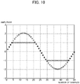
- FIG. 10 is a drawing illustrating a digital signal, of a number of period samples, of the composite waves (illustrated in FIGS. 5 and 6 ) constituted by the target wave and the interference wave, before and after clipping; and
- FIG. 11 is a graph illustrating the relationship between the amplification factor adjustment coefficient and the number of clipped samples.
- the present disclosure is made with the view of the above situation, and an objective of the present disclosure is to compensate for the level decrease of the target wave included in a signal that is clipped by an A-D converter.
- FIG. 1 is a block diagram illustrating a configuration example of a transceiver according to an embodiment of the present disclosure.
- a transceiver 100 includes an antenna 2 , a signal processing device 1 that processes signals received by the antenna 2 , a D-A converter 3 that digital-to-analog (D-A) converts the signals that are processed by the signal processing device 1 , an analog amplifier 4 that amplifies the signals that are D-A converted by the D-A converter 3 , and a speaker 5 that outputs the signals that are amplified by the analog amplifier 4 .
- the speaker 5 is an example of an output device.
- the signal processing device 1 includes an A-D converter 10 that A-D converts analog signals that are received by the antenna 2 , and a controller 20 that processes the digital signals that are A-D converted by the A-D converter 10 .
- the A-D converter 10 A-D converts analog signals that are received by the antenna 2 . At this time, if the amplitude of the analog signal exceeds a predetermined range, a digital signal, in which portions where the amplitude exceeds the predetermined range are clipped, is output from the A-D converter 10 .
- the A-D converter 10 outputs the converted digital signal to the controller 20 .
- the controller 20 performs processing, on the digital signal to be input, in order to compensate for level decreases of the target wave that are caused by the digital signal being clipped.
- the controller 20 outputs the processed digital signal to the D-A converter 3 .
- the controller 20 can be constituted in part or in whole by a digital signal processor (DSP) or in part or in whole by a field programmable gate array (FPGA).
- the controller 20 may also be constituted by a system on chip (SoC) that includes a CPU.
- SoC system on chip
- FIG. 1 only the receiving function of the transceiver 100 is illustrated, but the transceiver 100 may also include a sending function. Next, the processing performed by the signal processing device 1 is described in detail while referencing FIG. 2 .
- FIG. 2 is a block diagram illustrating a functional configuration example of the signal processing device according to an embodiment.
- the A-D converter 10 of the signal processing device 1 converts the analog signal to be input to a digital signal and outputs this digital signal to the controller 20 .
- the range of signal amplitudes that the A-D converter 10 can handle is determined.
- the antenna 2 receives both target waves and interference waves and, as a result, the amplitude of the analog signal received by the antenna 2 may exceed the predetermined range of the A-D converter 10 .
- portions of the analog signal, that is input into the A-D converter 10 from the antenna 2 , where the amplitude exceeds the predetermined range are clipped.
- the clipping of the analog signal is described using FIGS. 3 to 8 .
- FIG. 3 is a drawing illustrating an example of the target wave.
- FIG. 4 is a drawing illustrating an example of the interference wave.
- the range of signal amplitudes that the A-D converter 10 can handle is set to a range from ⁇ 1 to 1.
- the amplitude of the target wave illustrated in FIG. 3 is within the range from ⁇ 1 to 1, but the amplitude of the interference wave illustrated in FIG. 4 is outside the range from ⁇ 1 to 1.
- FIG. 5 is a drawing illustrating an example of an unclipped composite wave constituted by the target wave and the interference wave.
- the analog signal input into the A-D converter 10 is a composite wave such as that illustrated in FIG. 5 .
- the range of signal amplitudes that the A-D converter 10 can handle is the range from ⁇ 1 to 1.
- a waveform, in which the portions where the amplitude exceeds the range of ⁇ 1 to 1 are clipped is output as the digital signal.
- FIG. 6 is a drawing illustrating an example of a clipped composite wave constituted by the target wave and the interference wave.
- the A-D converter 10 outputs a signal in which the portions of the analog signal, of the composite wave, illustrated in FIG. 5 , constituted by the target wave and the interference wave, where the amplitude is ⁇ 1 or less and 1 or greater are clipped. Changes in the frequency spectrum of the composite wave constituted by the target wave and the interference wave due to being clipped are explained using FIGS. 7 and 8 .
- FIG. 7 is a drawing illustrating an example of the frequency spectrum of the unclipped composite wave illustrated in FIG. 5 , constituted by the target wave and the interference wave.
- the right section of FIG. 7 is an enlarged drawing of the range indicated by the dot-dash line in the left section.
- FIG. 8 is a drawing illustrating an example of the frequency spectrum of the clipped composite wave illustrated in FIG. 6 , constituted by the target wave and the interference wave.
- the right section of FIG. 8 is an enlarged drawing of the range indicated by the dot-dash line in the left section.
- the controller 20 performs processing on the digital signal that is input from the A-D converter 10 in order to compensate for the level decrease of the target wave.
- the controller 20 of the signal processing device 1 includes, as functional components, a frequency converter 21 , an LPF 22 , a rate converter 23 , a digital amplifier 24 , a counter 25 , and an amplification factor adjuster 26 .
- the frequency converter 21 performs frequency conversion on the digital signal input from the A-D converter 10 , such that the target wave is near 0 Hz. For example, in a case in which the target wave is 10 kHz, the frequency converter 21 multiplies the digital signal input from the A-D converter 10 by a 10 kHz sine wave signal. As a result, the frequency of the target wave becomes near 0 Hz, and the frequency of the unnecessary signal near 0 Hz increases to near 10 kHz.
- the LPF 22 removes the unnecessary high frequency components of the digital signal that was subjected to frequency conversion by the frequency converter 21 . As a result, the unnecessary frequency converted components and, also, the frequency components generated by the clipping are removed.
- the LPF 22 is an example of a filter.
- the filter is not limited to a low pass filter and may be any filter capable of removing the unnecessary signal components.
- the rate converter 23 outputs a value for each of N samples of the digital signal, from which the unnecessary high frequency components have been removed by the LPF 22 , and converts the sampling rate of the A-D converter 10 to 1/N-times.
- N is referred to as an “adjustment cycle.”
- the digital amplifier 24 amplifies the digital signal, for which the rate converter 23 has converted the sampling rate to 1/N-times, and outputs the amplified digital signal to the D-A converter 3 .
- the counter 25 calculates, for the digital signal input from the A-D converter 10 , a number of clipped samples C for each predetermined number of period samples P. Specifically, the counter 25 remembers the upper limit and the lower limit of the A-D converter 10 , counts the number of times the upper limit is reached and the number of times the lower limit is reached, and calculates these as the number of clipped samples C.
- the amplification factor adjuster 26 includes an amplification rate adjustment coefficient table that indicates the amplification factor adjustment coefficient that corresponds to the number of clipped samples C.
- FIG. 9 is a drawing illustrating an example of the amplification factor adjustment coefficient table.
- the number of period samples is 50.
- the amplification factor adjustment coefficient is a value obtained by dividing the number of period samples P by the number of unclipped regular samples R.
- the number of regular samples R is a value obtained by subtracting the number of clipped samples C from the number of period samples 50.
- the amplification factor adjuster 26 references the amplification factor adjustment coefficient table and multiplies a preset amplification factor ⁇ of the digital amplifier 24 by the amplification factor adjustment coefficient, thereby adjusting the amplification factor of the digital amplifier 24 .
- the digital amplifier 24 amplifies the digital signal by the amplification factor ⁇ amplification factor adjustment coefficient.
- the amplification factor adjustment coefficient is 1 and, as such, the digital amplifier 24 amplifies the digital signal by the preset amplification factor ⁇ .
- the amplification factor adjuster 26 calculates the amplification factor adjustment coefficient by dividing the number of period samples P by the number of regular samples R.
- FIG. 10 is a drawing illustrating a digital signal, of a number of period samples, of the composite waves (illustrated in FIGS. 5 and 6 ) constituted by the target wave and the interference wave, before and after clipping.
- the unclipped digital signal of the composite wave constituted by the target wave and the interference wave is indicated by the “+” symbol
- the clipped digital signal of the composite wave constituted by the target wave and the interference wave is indicated by the “ ⁇ ” symbol.
- the unclipped digital signal is depicted, but the digital signal that is actually input into the counter 25 is the clipped digital signal.
- the number of period samples P is 50 and the number of clipped samples C is 33.
- the amplification factor adjustment coefficient is 50/17.
- the amplification factor adjuster 26 multiplies the preset amplification factor ⁇ of the digital amplifier 24 by 50/17 to adjust the amplification factor of the digital amplifier 24 .
- ⁇ 50/17 is converted to decibels (dB)
- 20 log 10 (50/17) 9.7 dB.
- dB decibels
- the controller 20 compensates for the level decrease of the target wave.
- the digital amplifier 24 amplifies the digital signal by the ⁇ 50/17 amplification factor adjusted by the amplification factor adjuster 26 , and outputs the resulting digital signal to the D-A converter 3 .
- the number of period samples P is an integral multiple of the adjustment cycle N.
- the amplification factor adjuster 26 adjusts the amplification factor of the digital amplifier 24 every two times the rate converter 23 performs the processing of converting the sampling rate to 1/N-times.
- the number of period samples P is one-times the adjustment cycle N, that is, when the rate converter 23 converts the sampling rate 1/P-times, the processing becomes simple and the level decrease of the target wave is compensated for with greater precision.
- FIG. 11 is a graph illustrating the relationship between the number of clipped samples C and the value k obtained by dividing the number of period samples P by the number of regular samples R.
- the value k may be set as the amplification factor adjustment coefficient when the value k is less than a threshold, and the threshold may be set as the amplification factor adjustment coefficient when the value k is greater than or equal to this threshold.
- the threshold is recorded as the amplification factor adjustment coefficient, of the amplification factor adjustment coefficient table, that corresponds to the number of clipped samples C where the value, obtained by dividing the number of period samples P by the number of regular samples R, is greater than or equal to the threshold.
- the value k is greater than or equal to the threshold, a value that gradually increases from the threshold as the value k increases may be used as the amplification factor adjustment coefficient.
- a value that gradually increases from the threshold is recorded as the amplification factor adjustment coefficient, of the amplification factor adjustment coefficient table, that corresponds to the number of clipped samples C where the value, obtained by dividing the number of period samples P by the number of regular samples R, is greater than or equal to the threshold.
- the amplification factor of the digital amplifier 24 is adjusted on the basis of the ratio of the number of clipped samples C of the signal clipped by the A-D converter 10 . As a result, it is possible to compensate for the level decrease of the target wave included in the clipped signal.
- the embodiments of the present disclosure are not limited to the embodiments described above.
- applications of the signal processing device 1 are not limited to transceivers, and the signal processing device 1 can be applied to a device that converts an analog signal to be inputted to a digital signal in which portions having an amplitude that exceeds the predetermined range are clipped, subjects the converted digital signal to frequency conversion and sampling rate conversion, and amplifies the digital signal.
Abstract
A signal processing device includes an A-D converter and a controller. The A-D converter converts an analog signal to a digital signal in which portions where the amplitude exceeds a predetermined range are clipped. A counter of the controller calculates, for the digital signal, a number of clipped samples for each predetermined number of period samples. A frequency converter performs frequency conversion of the digital signal. An LPF removes high frequency components of the digital signal. A rate converter converts a sampling rate of the A-D converter. A digital amplifier amplifies and outputs the digital signal. An amplification factor adjuster multiplies a preset amplification factor of the digital amplifier by an amplification factor adjustment coefficient based on a ratio of the number of regular samples to the number of period samples, to adjust the amplification factor.
Description
This application claims the benefit of Japanese Patent Application No. 2018-225149, filed on Nov. 30, 2018, the entire disclosure of which is incorporated by reference herein.
The present disclosure relates generally to a signal processing device and a transceiver.
In cases where a target wave and an interference wave stronger than the target wave are simultaneously input into an analog-to-digital (A-D) converter of a transceiver and the amplitude of the composite wave constituted by the target wave and the interference wave exceeds the range determined by the A-D converter, portions of the input signal where the amplitude exceeds the predetermined range are clipped. When the input signal is clipped, the level of the target wave declines. In communication using an amplitude modulation method such as amplitude modulation (AM) or singe-sideband (SSB), information is transmitted by changing the amplitude of the radio waves. Accordingly, declines in the level of the target wave affect the communication. Due to this, there is a need to compensate for the level decline of the target wave of the clipped signal.
Unexamined Japanese Patent Application Kokai Publication No. H07-45000 discloses a digital audio sound playback device that suppresses clipping by adding negative offset voltage to portions of the waveform input into the A-D converter that exceed a predetermined range. Unexamined Japanese Patent Application Kokai Publication No. 2008-236268 discloses a clipping suppression device that suppresses clipping by extracting clipped portions of a series of input speech signals, smoothing the extracted portions, and adding the reverse phase of the smoothed signals to the speech signals. Unexamined Japanese Patent Application Kokai Publication No. 2003-099064 discloses a waveform correction method that includes interpolating and repairing a clipped portion of a recorded waveform.
A signal processing device according to a first aspect of the present disclosure includes:
an A-D converter that converts an analog signal that is input into the signal processing device to a digital signal in which portions where an amplitude exceeds a predetermined range are clipped, and outputs the digital signal; and
a controller that includes
a counter that calculates, for the digital signal output by the A-D converter, a number of clipped samples for each predetermined number of period samples;
a frequency converter that performs frequency conversion of the digital signal output by the A-D converter;
a filter that removes unnecessary signal components of the digital signal that is subjected to the frequency conversion by the frequency converter;
a rate converter that converts a sampling rate of the A-D converter to a sampling rate that is an integer multiple of a value obtained by dividing by the number of period samples;
a digital amplifier that amplifies the digital signal for which the rate converter has converted the sampling rate, and outputs the digital signal that is amplified; and
an amplification factor adjuster that multiplies a preset amplification factor of the digital amplifier by an amplification factor adjustment coefficient, based on a ratio of the number of clipped samples to the number of period samples, to adjust the amplification factor of the digital amplifier.
It is preferable that the amplification factor adjuster sets, as the amplification factor adjustment coefficient, a value obtained by dividing the number of period samples by a number of regular samples, which are unclipped.
It is preferable that:
when a value obtained by dividing the number of period samples by a number of regular samples that are unclipped is less than a threshold, the amplification factor adjuster sets, as the amplification factor adjustment coefficient, the value obtained by dividing the number of period samples by the number of regular samples, and
when the value obtained by dividing the number of period samples by the number of regular samples is greater than or equal to the threshold, the amplification factor adjuster sets the threshold as the amplification factor adjustment coefficient.
It is preferable that:
when a value obtained by dividing the number of period samples by a number of regular samples that are unclipped is less than a threshold, the amplification factor adjuster sets, as the amplification factor adjustment coefficient, the value obtained by dividing the number of period samples by the number of regular samples, and
when the value obtained by dividing the number of period samples by the number of regular samples is greater than or equal to the threshold, the amplification factor adjuster sets, as the amplification factor adjustment coefficient, a value that gradually increases from the threshold as the value obtained by dividing the number of period samples by the number of regular samples increases.
A transceiver according to a second aspect of the present disclosure includes:
any one of the signal processing devices;
an antenna that receives an analog signal and inputs the analog signal into the signal processing device;
a D-A converter that converts a digital signal, that is output by the signal processing device, to an analog signal;
an analog amplifier that amplifies the analog signal that is converted by the D-A converter; and
an output device that outputs the analog signal that is amplified by the analog amplifier.
According to the present disclosure, the amplification factor of the digital signal is adjusted on the basis of the ratio of the number of clipped samples of the digital signal that is converted by the A-D converter. As a result, it is possible to compensate for the level decrease of the target wave included in the clipped signal.
A more complete understanding of this application can be obtained when the following detailed description is considered in conjunction with the following drawings, in which:
The technologies disclosed in Unexamined Japanese Patent Application Kokai Publication No. H07-45000 and Unexamined Japanese Patent Application Kokai Publication No. 2008-236268 suppress clipping by processing unclipped signals, and do not include the compensation of clipped signals. While the technology disclosed in Unexamined Japanese Patent Application Kokai Publication No. 2003-099064 includes the compensation of clipped signals, this technology recovers the clipped portions from the unclipped portion by predicting. As such, in most cases, signals of frequency components that have weak levels, such as the target waves that are combined with strong interference waves, are not restored. Accordingly, when the technology of Patent Literature 3 is applied to a transceiver, level decreases of target waves of clipped signals are not compensated for.
The present disclosure is made with the view of the above situation, and an objective of the present disclosure is to compensate for the level decrease of the target wave included in a signal that is clipped by an A-D converter.
Hereinafter, embodiments of the present disclosure are described in detail while referencing the drawings. Note that, in the drawings, identical or equivalent components are marked with the same reference numerals.
The A-D converter 10 A-D converts analog signals that are received by the antenna 2. At this time, if the amplitude of the analog signal exceeds a predetermined range, a digital signal, in which portions where the amplitude exceeds the predetermined range are clipped, is output from the A-D converter 10. The A-D converter 10 outputs the converted digital signal to the controller 20. The controller 20 performs processing, on the digital signal to be input, in order to compensate for level decreases of the target wave that are caused by the digital signal being clipped. The controller 20 outputs the processed digital signal to the D-A converter 3. The controller 20 can be constituted in part or in whole by a digital signal processor (DSP) or in part or in whole by a field programmable gate array (FPGA). The controller 20 may also be constituted by a system on chip (SoC) that includes a CPU. In the example of FIG. 1 , only the receiving function of the transceiver 100 is illustrated, but the transceiver 100 may also include a sending function. Next, the processing performed by the signal processing device 1 is described in detail while referencing FIG. 2 .
Returning to FIG. 2 , the controller 20 of the signal processing device 1 includes, as functional components, a frequency converter 21, an LPF 22, a rate converter 23, a digital amplifier 24, a counter 25, and an amplification factor adjuster 26. The frequency converter 21 performs frequency conversion on the digital signal input from the A-D converter 10, such that the target wave is near 0 Hz. For example, in a case in which the target wave is 10 kHz, the frequency converter 21 multiplies the digital signal input from the A-D converter 10 by a 10 kHz sine wave signal. As a result, the frequency of the target wave becomes near 0 Hz, and the frequency of the unnecessary signal near 0 Hz increases to near 10 kHz. The LPF 22 removes the unnecessary high frequency components of the digital signal that was subjected to frequency conversion by the frequency converter 21. As a result, the unnecessary frequency converted components and, also, the frequency components generated by the clipping are removed. The LPF 22 is an example of a filter. The filter is not limited to a low pass filter and may be any filter capable of removing the unnecessary signal components. The rate converter 23 outputs a value for each of N samples of the digital signal, from which the unnecessary high frequency components have been removed by the LPF 22, and converts the sampling rate of the A-D converter 10 to 1/N-times. Hereinafter N is referred to as an “adjustment cycle.” The digital amplifier 24 amplifies the digital signal, for which the rate converter 23 has converted the sampling rate to 1/N-times, and outputs the amplified digital signal to the D-A converter 3.
The counter 25 calculates, for the digital signal input from the A-D converter 10, a number of clipped samples C for each predetermined number of period samples P. Specifically, the counter 25 remembers the upper limit and the lower limit of the A-D converter 10, counts the number of times the upper limit is reached and the number of times the lower limit is reached, and calculates these as the number of clipped samples C. The amplification factor adjuster 26 includes an amplification rate adjustment coefficient table that indicates the amplification factor adjustment coefficient that corresponds to the number of clipped samples C.
The digital amplifier 24 amplifies the digital signal by the α×50/17 amplification factor adjusted by the amplification factor adjuster 26, and outputs the resulting digital signal to the D-A converter 3. The number of period samples P is an integral multiple of the adjustment cycle N. For example, in a case in which the number of period samples P is twice the adjustment cycle N, the amplification factor adjuster 26 adjusts the amplification factor of the digital amplifier 24 every two times the rate converter 23 performs the processing of converting the sampling rate to 1/N-times. In a case in which the number of period samples P is one-times the adjustment cycle N, that is, when the rate converter 23 converts the sampling rate 1/P-times, the processing becomes simple and the level decrease of the target wave is compensated for with greater precision.
As described above, with the signal processing device 1 according to the present embodiment, the amplification factor of the digital amplifier 24 is adjusted on the basis of the ratio of the number of clipped samples C of the signal clipped by the A-D converter 10. As a result, it is possible to compensate for the level decrease of the target wave included in the clipped signal.
The embodiments of the present disclosure are not limited to the embodiments described above. For example, applications of the signal processing device 1 are not limited to transceivers, and the signal processing device 1 can be applied to a device that converts an analog signal to be inputted to a digital signal in which portions having an amplitude that exceeds the predetermined range are clipped, subjects the converted digital signal to frequency conversion and sampling rate conversion, and amplifies the digital signal.
The foregoing describes some example embodiments for explanatory purposes. Although the foregoing discussion has presented specific embodiments, persons skilled in the art will recognize that changes may be made in form and detail without departing from the broader spirit and scope of the invention. Accordingly, the specification and drawings are to be regarded in an illustrative rather than a restrictive sense. This detailed description, therefore, is not to be taken in a limiting sense, and the scope of the invention is defined only by the included claims, along with the full range of equivalents to which such claims are entitled.
Claims (8)
1. A signal processing device, comprising:
an A-D converter that converts an analog signal, that is input into the signal processing device, to a digital signal in which portions where an amplitude exceeds a predetermined range are clipped, and outputs the digital signal; and
a controller that includes:
a counter that calculates, for the digital signal output by the A-D converter, a number of clipped samples for each predetermined number of period samples;
a frequency converter that performs frequency conversion of the digital signal output by the A-D converter;
a filter that removes unnecessary signal components of the digital signal that is subjected to the frequency conversion by the frequency converter;
a rate converter that converts a sampling rate of the A-D converter to a sampling rate that is an integer multiple of a value obtained by dividing by the number of period samples;
a digital amplifier that amplifies the digital signal for which the rate converter has converted the sampling rate, and outputs the digital signal that is amplified; and
an amplification factor adjuster that multiplies a preset amplification factor of the digital amplifier by an amplification factor adjustment coefficient, based on a ratio of the number of clipped samples to the number of period samples, to adjust the amplification factor of the digital amplifier.
2. The signal processing device according to claim 1 , wherein the amplification factor adjuster sets a value obtained by dividing the number of period samples by a number of regular samples that are unclipped as the amplification factor adjustment coefficient.
3. The signal processing device according to claim 1 , wherein
when a value obtained by dividing the number of period samples by a number of regular samples that are unclipped is less than a threshold, the amplification factor adjuster sets, as the amplification factor adjustment coefficient, the value obtained by dividing the number of period samples by the number of regular samples, and
when the value obtained by dividing the number of period samples by the number of regular samples is greater than or equal to the threshold, the amplification factor adjuster sets the threshold as the amplification factor adjustment coefficient.
4. The signal processing device according to claim 1 , wherein
when a value obtained by dividing the number of period samples by a number of regular samples that are unclipped is less than a threshold, the amplification factor adjuster sets, as the amplification factor adjustment coefficient, the value obtained by dividing the number of period samples by the number of regular samples, and
when the value obtained by dividing the number of period samples by the number of regular samples is greater than or equal to the threshold, the amplification factor adjuster sets, as the amplification factor adjustment coefficient, a value that gradually increases from the threshold as the value obtained by dividing the number of period samples by the number of regular samples increases.
5. A transceiver, comprising:
the signal processing device according to claim 1 ;
an antenna that receives an analog signal and inputs the analog signal into the signal processing device;
a D-A converter that converts a digital signal, that is output by the signal processing device, to an analog signal;
an analog amplifier that amplifies the analog signal that is converted by the D-A converter; and
an output device that outputs the analog signal that is amplified by the analog amplifier.
6. A transceiver, comprising:
the signal processing device according to claim 2 ;
an antenna that receives an analog signal and inputs the analog signal into the signal processing device;
a D-A converter that converts a digital signal, that is output by the signal processing device, to an analog signal;
an analog amplifier that amplifies the analog signal that is converted by the D-A converter; and
an output device that outputs the analog signal that is amplified by the analog amplifier.
7. A transceiver, comprising:
the signal processing device according to claim 3 ;
an antenna that receives an analog signal and inputs the analog signal into the signal processing device;
a D-A converter that converts a digital signal, that is output by the signal processing device, to an analog signal;
an analog amplifier that amplifies the analog signal that is converted by the D-A converter; and
an output device that outputs the analog signal that is amplified by the analog amplifier.
8. A transceiver, comprising:
the signal processing device according to claim 4 ;
an antenna that receives an analog signal and inputs the analog signal into the signal processing device;
a D-A converter that converts a digital signal, that is output by the signal processing device, to an analog signal;
an analog amplifier that amplifies the analog signal that is converted by the D-A converter; and
an output device that outputs the analog signal that is amplified by the analog amplifier.
Applications Claiming Priority (2)
| Application Number | Priority Date | Filing Date | Title |
|---|---|---|---|
| JP2018-225149 | 2018-11-30 | ||
| JP2018225149A JP7089183B2 (en) | 2018-11-30 | 2018-11-30 | Signal processing equipment and radios |
Publications (2)
| Publication Number | Publication Date |
|---|---|
| US20200177196A1 US20200177196A1 (en) | 2020-06-04 |
| US10797717B2 true US10797717B2 (en) | 2020-10-06 |
Family
ID=70850847
Family Applications (1)
| Application Number | Title | Priority Date | Filing Date |
|---|---|---|---|
| US16/654,499 Active US10797717B2 (en) | 2018-11-30 | 2019-10-16 | Signal processing device and transceiver |
Country Status (2)
| Country | Link |
|---|---|
| US (1) | US10797717B2 (en) |
| JP (1) | JP7089183B2 (en) |
Citations (14)
| Publication number | Priority date | Publication date | Assignee | Title |
|---|---|---|---|---|
| JPH0745000A (en) | 1993-07-28 | 1995-02-14 | Nippon Columbia Co Ltd | Device for sound recording/reproducing digital audio |
| US6323907B1 (en) * | 1996-10-01 | 2001-11-27 | Hyundai Electronics Industries Co., Ltd. | Frequency converter |
| JP2003099064A (en) | 2001-09-21 | 2003-04-04 | Yamaha Corp | Waveform correcting method |
| JP2008236268A (en) | 2007-03-19 | 2008-10-02 | Fujitsu Ltd | Clip suppressing device and clip suppression program |
| US20090245437A1 (en) * | 2008-03-27 | 2009-10-01 | Kabushiki Kaisha Toshiba | Sample rate converter and rceiver using the same |
| US20110069787A1 (en) * | 2009-09-24 | 2011-03-24 | Korea Advanced Institute Of Science & Technology | Apparatus and Method for Processing Multi-Channel Signals and Multi-Channel Receiver Using the Same |
| US20130201045A1 (en) * | 2012-02-03 | 2013-08-08 | Sigear Europe Sàrl | Digital-to-Analog Converter Implementing Hybrid Conversion Architecture |
| US20140043177A1 (en) * | 2011-06-27 | 2014-02-13 | Syntropy Systems, Llc | Apparatuses and Methods for Linear to Discrete Quantization Conversion with Reduced Sampling Variation Errors |
| US20140340161A1 (en) * | 2013-05-15 | 2014-11-20 | Asahi Kasei Microdevices Corporation | Digital phase-locked loop device with automatic frequency range selection |
| US9363126B2 (en) * | 2007-12-21 | 2016-06-07 | Google Technology Holdings LLC | Method and apparatus for IFDMA receiver architecture |
| US20170170838A1 (en) * | 2011-06-27 | 2017-06-15 | Syntropy Systems, Llc | Apparatuses and Methods for Converting Fluctuations in Periodicity of an Input Signal into Fluctuations in Amplitude of an Output Signal |
| US9837990B1 (en) * | 2015-12-11 | 2017-12-05 | Syntropy Systems, Llc | Digital signal processor |
| US20190238152A1 (en) * | 2011-06-27 | 2019-08-01 | Syntropy Systems, Llc | Apparatuses and Methods for Sample Rate Conversion |
| US20200153406A1 (en) * | 2005-09-27 | 2020-05-14 | Ronald Quan | Method and apparatus to evaluate audio equipment for dynamic distortions and or differential phase and or frequency modulation effects |
Family Cites Families (8)
| Publication number | Priority date | Publication date | Assignee | Title |
|---|---|---|---|---|
| JPH09162739A (en) * | 1995-12-05 | 1997-06-20 | Sony Corp | Digital signal processor |
| GB2369258B (en) | 2000-11-21 | 2005-06-15 | Ubinetics Ltd | A radio receiver |
| JP2004134917A (en) | 2002-10-09 | 2004-04-30 | Matsushita Electric Ind Co Ltd | Automatic gain control apparatus, wireless receiver, and automatic gain control method |
| JP4539539B2 (en) | 2005-11-18 | 2010-09-08 | 株式会社デンソー | Soft decision value correction method, receiver, program |
| JP4922023B2 (en) | 2007-03-09 | 2012-04-25 | 株式会社東芝 | Analog-digital conversion device, wireless communication terminal, and program |
| EP2485395B1 (en) | 2011-02-04 | 2013-05-01 | Harman International Industries Ltd. | Audio Mixing Console avoiding Signal Level Overload |
| JP5845934B2 (en) | 2012-01-30 | 2016-01-20 | 株式会社Jvcケンウッド | Asynchronous sampling frequency converter, conversion method, and program |
| WO2018092581A1 (en) | 2016-11-16 | 2018-05-24 | 株式会社日立国際電気 | Radio device |
-
2018
- 2018-11-30 JP JP2018225149A patent/JP7089183B2/en active Active
-
2019
- 2019-10-16 US US16/654,499 patent/US10797717B2/en active Active
Patent Citations (14)
| Publication number | Priority date | Publication date | Assignee | Title |
|---|---|---|---|---|
| JPH0745000A (en) | 1993-07-28 | 1995-02-14 | Nippon Columbia Co Ltd | Device for sound recording/reproducing digital audio |
| US6323907B1 (en) * | 1996-10-01 | 2001-11-27 | Hyundai Electronics Industries Co., Ltd. | Frequency converter |
| JP2003099064A (en) | 2001-09-21 | 2003-04-04 | Yamaha Corp | Waveform correcting method |
| US20200153406A1 (en) * | 2005-09-27 | 2020-05-14 | Ronald Quan | Method and apparatus to evaluate audio equipment for dynamic distortions and or differential phase and or frequency modulation effects |
| JP2008236268A (en) | 2007-03-19 | 2008-10-02 | Fujitsu Ltd | Clip suppressing device and clip suppression program |
| US9363126B2 (en) * | 2007-12-21 | 2016-06-07 | Google Technology Holdings LLC | Method and apparatus for IFDMA receiver architecture |
| US20090245437A1 (en) * | 2008-03-27 | 2009-10-01 | Kabushiki Kaisha Toshiba | Sample rate converter and rceiver using the same |
| US20110069787A1 (en) * | 2009-09-24 | 2011-03-24 | Korea Advanced Institute Of Science & Technology | Apparatus and Method for Processing Multi-Channel Signals and Multi-Channel Receiver Using the Same |
| US20140043177A1 (en) * | 2011-06-27 | 2014-02-13 | Syntropy Systems, Llc | Apparatuses and Methods for Linear to Discrete Quantization Conversion with Reduced Sampling Variation Errors |
| US20170170838A1 (en) * | 2011-06-27 | 2017-06-15 | Syntropy Systems, Llc | Apparatuses and Methods for Converting Fluctuations in Periodicity of an Input Signal into Fluctuations in Amplitude of an Output Signal |
| US20190238152A1 (en) * | 2011-06-27 | 2019-08-01 | Syntropy Systems, Llc | Apparatuses and Methods for Sample Rate Conversion |
| US20130201045A1 (en) * | 2012-02-03 | 2013-08-08 | Sigear Europe Sàrl | Digital-to-Analog Converter Implementing Hybrid Conversion Architecture |
| US20140340161A1 (en) * | 2013-05-15 | 2014-11-20 | Asahi Kasei Microdevices Corporation | Digital phase-locked loop device with automatic frequency range selection |
| US9837990B1 (en) * | 2015-12-11 | 2017-12-05 | Syntropy Systems, Llc | Digital signal processor |
Also Published As
| Publication number | Publication date |
|---|---|
| JP2020088789A (en) | 2020-06-04 |
| JP7089183B2 (en) | 2022-06-22 |
| US20200177196A1 (en) | 2020-06-04 |
Similar Documents
| Publication | Publication Date | Title |
|---|---|---|
| US7742746B2 (en) | Automatic volume and dynamic range adjustment for mobile audio devices | |
| US9672834B2 (en) | Dynamic range compression with low distortion for use in hearing aids and audio systems | |
| US20130136266A1 (en) | System for Dynamic Spectral Correction of Audio Signals to Compensate for Ambient Noise | |
| US20040234006A1 (en) | Reducing peak-to-average signal power ratio | |
| AU2009242464A1 (en) | System and method for dynamic sound delivery | |
| US8000408B2 (en) | Loop delay and gain control methods in closed-loop transmitters and wireless devices | |
| JP2011019164A (en) | Peak factor reduction device and base station | |
| US9473102B2 (en) | Level adjusting circuit, digital sound processor, audio AMP integrated circuit, electronic apparatus and method of automatically adjusting level of audio signal | |
| US8144762B2 (en) | Band extending apparatus and method | |
| US10797717B2 (en) | Signal processing device and transceiver | |
| US8385834B2 (en) | Radio receiving apparatus and noise elimination method in the same apparatus | |
| US20230299860A1 (en) | Reception device and a/d conversion method | |
| US10043530B1 (en) | Method and audio noise suppressor using nonlinear gain smoothing for reduced musical artifacts | |
| JP4288458B2 (en) | Amplitude limiting circuit and CDMA communication apparatus | |
| US11509321B2 (en) | Receiving circuit and associated signal processing method | |
| JP5100339B2 (en) | Power amplifier | |
| CN109525264B (en) | Adaptive signal compressor for AM radio | |
| US20100219909A1 (en) | Harmonic suppressing circuit | |
| US9940946B2 (en) | Sharp noise suppression | |
| KR100325137B1 (en) | Digital auto gain controller in communication system | |
| US9756441B2 (en) | Digital wireless audio transmission system with optimized dynamics | |
| CN111724800B (en) | Moss code audio noise reduction method and noise reduction earphone using same | |
| CN108235183B (en) | Automatic gain control amplitude limiting method capable of keeping effective dynamic range of voice digital signal and preventing peak clipping | |
| EP2602933B1 (en) | Analog signal transfer system, variable compressor and variable expander | |
| KR100625238B1 (en) | Apparatus for automatically controlling gain in orthogonal frequency division multiple access system |
Legal Events
| Date | Code | Title | Description |
|---|---|---|---|
| FEPP | Fee payment procedure |
Free format text: ENTITY STATUS SET TO UNDISCOUNTED (ORIGINAL EVENT CODE: BIG.); ENTITY STATUS OF PATENT OWNER: LARGE ENTITY |
|
| STPP | Information on status: patent application and granting procedure in general |
Free format text: NOTICE OF ALLOWANCE MAILED -- APPLICATION RECEIVED IN OFFICE OF PUBLICATIONS |
|
| STPP | Information on status: patent application and granting procedure in general |
Free format text: PUBLICATIONS -- ISSUE FEE PAYMENT VERIFIED |
|
| STCF | Information on status: patent grant |
Free format text: PATENTED CASE |
|
| MAFP | Maintenance fee payment |
Free format text: PAYMENT OF MAINTENANCE FEE, 4TH YEAR, LARGE ENTITY (ORIGINAL EVENT CODE: M1551); ENTITY STATUS OF PATENT OWNER: LARGE ENTITY Year of fee payment: 4 |