US10795523B2 - Sense electrode design - Google Patents
Sense electrode design Download PDFInfo
- Publication number
- US10795523B2 US10795523B2 US16/431,689 US201916431689A US10795523B2 US 10795523 B2 US10795523 B2 US 10795523B2 US 201916431689 A US201916431689 A US 201916431689A US 10795523 B2 US10795523 B2 US 10795523B2
- Authority
- US
- United States
- Prior art keywords
- spine
- crossbars
- sense
- electrodes
- drive electrodes
- Prior art date
- Legal status (The legal status is an assumption and is not a legal conclusion. Google has not performed a legal analysis and makes no representation as to the accuracy of the status listed.)
- Active
Links
Images


Classifications
-
- G—PHYSICS
- G06—COMPUTING; CALCULATING OR COUNTING
- G06F—ELECTRIC DIGITAL DATA PROCESSING
- G06F3/00—Input arrangements for transferring data to be processed into a form capable of being handled by the computer; Output arrangements for transferring data from processing unit to output unit, e.g. interface arrangements
- G06F3/01—Input arrangements or combined input and output arrangements for interaction between user and computer
- G06F3/03—Arrangements for converting the position or the displacement of a member into a coded form
- G06F3/041—Digitisers, e.g. for touch screens or touch pads, characterised by the transducing means
- G06F3/044—Digitisers, e.g. for touch screens or touch pads, characterised by the transducing means by capacitive means
- G06F3/0446—Digitisers, e.g. for touch screens or touch pads, characterised by the transducing means by capacitive means using a grid-like structure of electrodes in at least two directions, e.g. using row and column electrodes
-
- G—PHYSICS
- G06—COMPUTING; CALCULATING OR COUNTING
- G06F—ELECTRIC DIGITAL DATA PROCESSING
- G06F3/00—Input arrangements for transferring data to be processed into a form capable of being handled by the computer; Output arrangements for transferring data from processing unit to output unit, e.g. interface arrangements
- G06F3/01—Input arrangements or combined input and output arrangements for interaction between user and computer
- G06F3/03—Arrangements for converting the position or the displacement of a member into a coded form
- G06F3/041—Digitisers, e.g. for touch screens or touch pads, characterised by the transducing means
- G06F3/044—Digitisers, e.g. for touch screens or touch pads, characterised by the transducing means by capacitive means
- G06F3/0443—Digitisers, e.g. for touch screens or touch pads, characterised by the transducing means by capacitive means using a single layer of sensing electrodes
-
- Y—GENERAL TAGGING OF NEW TECHNOLOGICAL DEVELOPMENTS; GENERAL TAGGING OF CROSS-SECTIONAL TECHNOLOGIES SPANNING OVER SEVERAL SECTIONS OF THE IPC; TECHNICAL SUBJECTS COVERED BY FORMER USPC CROSS-REFERENCE ART COLLECTIONS [XRACs] AND DIGESTS
- Y10—TECHNICAL SUBJECTS COVERED BY FORMER USPC
- Y10T—TECHNICAL SUBJECTS COVERED BY FORMER US CLASSIFICATION
- Y10T29/00—Metal working
- Y10T29/49—Method of mechanical manufacture
- Y10T29/49002—Electrical device making
Definitions
- Touchscreen displays are able to detect a touch such as by a finger or stylus within an active or display area.
- a touchscreen as part of a display enables a user to interact with an electronic application by touching the touchscreen.
- the display may present images to the user. Such images may include user interface constructs such as different buttons, images, or other regions that can be selected, manipulated, or actuated by touch.
- Touchscreens can therefore provide an effective user interface for cell phones, GPS devices, personal digital assistants (PDAs), computers, ATM machines, appliances and other devices.
- PDAs personal digital assistants
- Touchscreens use various technologies to sense touch from a finger or stylus, such as resistive, capacitive, infrared, and acoustic sensors.
- Capacitive touchscreens often use one or more layers of transverse electrodes, drive electrodes and sense electrodes.
- a touch changes a capacitance at a node in an array of electrodes overlaying the display device.
- a node is typically thought of as the area where a drive electrode and a receive electrode overlap or otherwise run adjacent.
- Transparent electrodes such as indium tin oxide (ITO) or transparent conductive polymers may be used to form the electrodes.
- Some layouts of electrodes utilize a flooded type pattern of drive electrodes to shield the sense electrodes from electric field interference from an underlying display such as a liquid crystal display (LCD).
- the flooded type pattern may use solid fill drive electrode patterns formed in a layer between the sense electrodes and display.
- the layer of electrodes closest to the display are the drive electrodes, and run in a first direction.
- the sense electrodes include spines that run transverse to the drive electrodes, and may also include crossbars that run in the same direction as the drive electrodes.
- the resistance to connection lines from portions of the crossbar electrode farthest from connection lines on the touchscreen is greater than the resistance to connection lines from portions of the crossbars closer to the connection lines.
- the electronics may contain sense circuitry having a sense capacitor. The sense circuitry operate to accommodate a worst case charge transfer time, having resistive and capacitive components, to allow sufficient charge to transfer from the drive electrodes through the sense electrodes to the sense capacitor. Long charge transfer times could significantly slow down the operation of the touchscreen.
- FIG. 1A is a schematic representation of an electrode layout for a touch sensitive device according to an example embodiment.
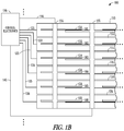
- FIG. 1B is a schematic representation of an alternative electrode layout for a touch sensitive device according to an example embodiment.
- FIG. 2 is a schematic representation of an alternative sense electrode layout according to an example embodiment.
- FIG. 3 is a schematic representation of a further alternative sense electrode layout according to an example embodiment.
- FIG. 4 is a schematic representation of a further alternative sense electrode layout for a touch sensitive device according to an example embodiment.
- FIGS. 1A and 1B are schematic representations of an electrode layout for an example touch sensitive device 100 such as a touchscreen.
- a plurality of longitudinal drive electrodes 110 , 112 , 114 , 116 , 118 , and 120 are formed in one layer.
- the drive electrodes may also be referred to as X electrodes.
- the drive electrodes are bar shaped, and completely filled in to help create a shield from electric field interference from an underlying display device, such as a liquid crystal display (LCD).
- This type of drive electrode layout may be referred to as a flooded X pattern.
- the distance between the drive electrodes may be minimized in one embodiment to provide better shielding.
- the dimensions shown in the drawings may not be to scale and are not meant to be an accurate representation of the dimensions that may be used in various embodiments, but rather may be exaggerated to more clearly illustrate the concepts described herein.
- the drive electrodes 110 , 112 , 114 , 116 , 118 , and 120 may be other than rectangular in shape, and may have more of a zig-zag pattern to minimize their visibility.
- the drive electrodes 110 , 112 , 114 , 116 , 118 , and 120 may be coupled via drive lines 121 , 122 , 123 , 124 , 125 , and 126 to electronics 130 to drive the drive electrodes during operation of the touch sensitive device 100 .
- one or more sense electrodes 135 , 137 may run transverse to the drive electrodes.
- the sense electrodes 135 , 137 may be formed of a conductive transparent material such as indium tin oxide (ITO) or transparent conductive polymers. Such materials, which while conductive, have a resistance. The resistance of electrodes made of such materials may change depending on the width of the electrode.
- the sense electrodes 135 , 137 may be coupled to electronics 130 via connection lines 140 and 142 respectively.
- the connection lines 140 and 142 may be highly conductive and formed of metal.
- the sense electrodes are single connected in one embodiment, in that only one end of the sense electrodes is coupled to the electronics 130 .
- sense electrodes 135 and 137 include a spine that runs transverse to the drive electrodes, and may also include crossbars transverse to the spine of sense electrode 135 and having different widths as indicated at 150 , 152 , 154 , 156 , 158 , and 160 .
- the crossbars run in the same direction as corresponding drive electrodes and are positioned over the respective drive electrodes 110 , 112 , 114 , 116 , 118 , and 120 .
- the crossbars extend from both sides of the spines, and have tips indicated on one end of the crossbars at 161 , 162 , 163 , 164 , 165 , and 166 that are the furthest distance from the spine 135 .
- the other ends of the crossbars may be the same distance from the spine 135 in various embodiments.
- the width of the crossbars in one embodiment increases with distance from the end of the spines coupled to the connection lines 140 , 142 .
- the increase in width decreases the resistance of the crossbars while increasing their capacitance to the drive electrodes.
- the increase in width keeps the charge transfer time of each crossbar at or under a desired threshold.
- the charge transfer time is the time it takes to transfer sufficient charge from the drive electrodes through the sense electrodes to the sense capacitor.
- the charge transfer time of each crossbar is substantially equal, taking into account process tolerances.
- the width of crossbar 150 is fairly narrow.
- the width increases with successive crossbars 152 - 160 such that the widest crossbar 160 is furthest from the connection line 140 .
- the width of the spine of sense electrode 135 may be approximately 1 mm, and the width of the crossbars may progress from 0.2 mm to 0.5 mm or wider, including wider than the spine in some embodiments.
- spine 137 has corresponding crossbars, as would additional spines as represented by the dots.
- the crossbars from adjacent spines may run adjacent to each other in further embodiments.
- the crossbars extend about 75 percent of the distance between the spines, and thus run adjacent together for about 50 percent of their length as shown. The amount of adjacent run may vary in further embodiments.
- the spines may be narrower or wider than 1 mm in various embodiments consistent with desired charge transfer time and visibility constraints.
- the widths of the crossbars may be determined by starting with the worst case charge transfer time.
- the worst case charge transfer time would be the longest path from tip 166 of crossbar 160 , along the spine of sense electrode 135 to connection line 140 .
- the remaining crossbar widths are chosen to obtain charge transfer times equal to or less than the desired charge transfer time.
- the charge transfer time is generally a function of a resistance and a capacitance, where the resistance is the resistance from crossbar tip to the connection line of the sense electrode, and the capacitance is the capacitance between the drive electrodes and the sense electrode.
- the capacitance is affected by touch proximate the intersection of a sense electrode and a drive electrode.
- the worst case charge transfer time, T may be calculated and used as a threshold or design parameter for ensuring that the charge transfer time at the tips of each crossbar is less than the worst case T, or equal to it. This results in the illustrated pattern of crossbar widths increasing with increased distance from the connection line.
- the capacitance may be reduced over the length of the sense electrodes.
- Sense electrodes may be increased in width to reduce the worst case charge transfer time.
- the use of wider crossbars for selected crossbars allows a reduction in the worst case charge transfer time.
- Narrower crossbars for selected crossbars reduces the capacitive coupling between the sense electrodes and the drive electrodes and hence allows a reduction in overall thickness of sensing portions of touch sensitive devices. This reduction in sense electrode layer thickness may result in a reduced overall touch sensitive device thickness, and may further reduce drive electrode to sense electrode separation.
- the worst case charge transfer time may be reduced by making some of the crossbars wider, while others already having a shorter charge transfer time may be made narrower.
- a sense electrode design may be optimized by making a worst case charge transfer time equal at all extremes of the electrode design.
- Such designs may or may not include crossbars, and the extremes of the design may or may not have electrode structures with equal widths. The charge transfer times of such sense electrodes should be substantially equal such that the charge transfer time does not adversely impact operation of a touch sensitive device.
- the extremes of the design may correspond to portions of the electrode design that are furthest from a connection line that has a relatively higher conductivity than that of the electrode.
- the extremes of the electrode design may additionally correspond to portions of the electrode design that have smaller widths than other portions of the design, and may not directly correspond to portions of the design that are furthest from higher conductivity connection lines.
- the width of such portions may be modified to ensure that the sense electrodes have a charge transfer time that is equal to or better than a desired worst case charge transfer time.
- FIG. 1B shows sense electrodes with varying crossbar widths as described above.
- adjacent sense electrodes are arranged to be coupled to connection lines on alternate opposite ends. This results in the width of electrodes progressing along the spines from alternate opposite ends.
- the adjacent crossbars from adjacent spines are arranged such that the widest crossbars runs adjacent to the narrowest crossbars, while crossbars of medium width run adjacent to each other.
- the combined width of the adjacent crossbars may be fairly equal in some embodiments over the length of the spines.
- FIG. 2 is a schematic representation of an alternative sense electrode layout 200 according to an example embodiment.
- Layout 200 shows one sense electrode 210 having a spine 215 with multiple transverse crossbars 220 , 221 , 222 , 223 , 224 , 225 , and 226 .
- Sense electrode 210 in one embodiment is double connected, meaning that both ends of the sense electrode 210 are coupled to connection lines as indicated by connection lines 230 and 235 .
- connection lines 230 and 235 are coupled together for coupling to a controller to individually sense signals from the electrodes. Since sense electrode 210 is connected on both ends, the crossbar being furthest from a connection line is actually the middle crossbar 223 .
- Crossbar 223 would be the crossbar exhibiting the worst case charge transfer time, but as shown, it has been widened to obtain a desired charge transfer time.
- the crossbars continue to decrease in width in both directions from crossbar 223 toward respective connection lines 230 and 235 .
- crossbars 222 and 224 may be equal in width
- crossbars 221 and 225 may be equal in width
- crossbars 220 and 226 may also be equal in width.
- the rest of the crossbars may be successively narrower, as there is no need to make them as wide as the widest crossbar.
- the charge transfer time from the tip of each crossbar to the nearest connection line be equal, meaning that the width is decreased as the distance to the nearest connection line decreases.
- Additional sense electrodes that have the varying width crossbar arrangement may be provided as indicated by the additional sense electrode with crossbars running adjacent crossbars 220 , 221 , 222 , 223 , 224 , 225 , and 226 , and dots indicating a repeating pattern of sense electrodes. It is understood that the dimensions of FIG. 2 , as well as the other drawings, may not be to scale and are not meant to be an accurate representation of the dimensions that may be used in various embodiments, but rather, the dimensions may be exaggerated to more clearly illustrate the concepts described herein.
- FIG. 3 is a schematic representation of a further alternative sense electrode layout 300 according to an example embodiment.
- Layout 300 includes a sense electrode 310 having different widths 312 , 314 , 316 , and 318 along its spine.
- Several transverse crossbars 320 , 322 , 324 , and 326 are shown coupled to the sense electrode 310 .
- the width of the spine increases with increasing distance from a single connected connection line 330 .
- a crossbar is coupled to the sense electrode.
- the crossbars may be connected at other points on the sense electrode where the sense electrode does not transition in width.
- the width of the sense electrode may continuously vary, or may vary in a stepwise manner, with multiple crossbars coupled to each section of constant width.
- Various embodiments may include adjacent sense electrodes arranged to be coupled to connection lines on alternate opposite ends as illustrated in FIG. 1B .
- the crossbars 320 , 322 , 324 and 326 are also shown as varying in their width.
- the worst case charge transfer time from a tip of the crossbar farthest from the connection line 330 may be used. In this case, that would be crossbar 326 .
- the charge transfer time again is the total charge transfer time from the tip of the crossbar 326 to the connection line 330 .
- the charge transfer time may be reduced by the fact that the spine is increasing in width.
- the width of crossbar 326 may not be as wide as in previous embodiments to meet a desired worst case charge transfer time.
- the same reduction in width for succeeding crossbars closer to connection line 330 may also be obtained.
- additional spines with crossbars may be provided in various patterns to obtain a pattern having a desired area.
- FIG. 4 is a schematic representation of a further alternative sense electrode layout 400 for a touch screen.
- Six spines 410 , 412 , 414 , 416 , 418 and 420 are shown and representative of sense electrodes for an entire touchscreen in one embodiment.
- Each of the spines may be double connected such that both ends may be coupled to sense circuitry. Similar to FIG. 2 , each spine has multiple transverse crossbars. Twenty nine crossbars per spine are illustrated. Since the spines are connected on both ends, the crossbar being furthest from a low resistance connection (not shown) to the sense circuitry is actually the middle crossbar 425 , which is the 15th crossbar from either end of the spines.
- Crossbar 425 is thus the crossbar exhibiting the worst case charge transfer time until it is widened as shown to obtain a desired charge transfer time. The crossbars continue to decrease in width in both directions from crossbar 425 toward respective connections to sense circuitry.
Abstract
Description
Claims (10)
Priority Applications (2)
| Application Number | Priority Date | Filing Date | Title |
|---|---|---|---|
| US16/431,689 US10795523B2 (en) | 2009-10-26 | 2019-06-04 | Sense electrode design |
| US17/062,674 US20210081077A1 (en) | 2009-10-26 | 2020-10-05 | Sense Electrode Design |
Applications Claiming Priority (4)
| Application Number | Priority Date | Filing Date | Title |
|---|---|---|---|
| US12/605,779 US9916045B2 (en) | 2009-10-26 | 2009-10-26 | Sense electrode design |
| US15/915,726 US10228808B2 (en) | 2009-10-26 | 2018-03-08 | Sense electrode design |
| US16/277,636 US10338759B1 (en) | 2009-10-26 | 2019-02-15 | Sense electrode design |
| US16/431,689 US10795523B2 (en) | 2009-10-26 | 2019-06-04 | Sense electrode design |
Related Parent Applications (1)
| Application Number | Title | Priority Date | Filing Date |
|---|---|---|---|
| US16/277,636 Continuation US10338759B1 (en) | 2009-10-26 | 2019-02-15 | Sense electrode design |
Related Child Applications (1)
| Application Number | Title | Priority Date | Filing Date |
|---|---|---|---|
| US17/062,674 Continuation US20210081077A1 (en) | 2009-10-26 | 2020-10-05 | Sense Electrode Design |
Publications (2)
| Publication Number | Publication Date |
|---|---|
| US20190391688A1 US20190391688A1 (en) | 2019-12-26 |
| US10795523B2 true US10795523B2 (en) | 2020-10-06 |
Family
ID=43897999
Family Applications (5)
| Application Number | Title | Priority Date | Filing Date |
|---|---|---|---|
| US12/605,779 Active 2036-08-23 US9916045B2 (en) | 2009-10-26 | 2009-10-26 | Sense electrode design |
| US15/915,726 Expired - Fee Related US10228808B2 (en) | 2009-10-26 | 2018-03-08 | Sense electrode design |
| US16/277,636 Expired - Fee Related US10338759B1 (en) | 2009-10-26 | 2019-02-15 | Sense electrode design |
| US16/431,689 Active US10795523B2 (en) | 2009-10-26 | 2019-06-04 | Sense electrode design |
| US17/062,674 Abandoned US20210081077A1 (en) | 2009-10-26 | 2020-10-05 | Sense Electrode Design |
Family Applications Before (3)
| Application Number | Title | Priority Date | Filing Date |
|---|---|---|---|
| US12/605,779 Active 2036-08-23 US9916045B2 (en) | 2009-10-26 | 2009-10-26 | Sense electrode design |
| US15/915,726 Expired - Fee Related US10228808B2 (en) | 2009-10-26 | 2018-03-08 | Sense electrode design |
| US16/277,636 Expired - Fee Related US10338759B1 (en) | 2009-10-26 | 2019-02-15 | Sense electrode design |
Family Applications After (1)
| Application Number | Title | Priority Date | Filing Date |
|---|---|---|---|
| US17/062,674 Abandoned US20210081077A1 (en) | 2009-10-26 | 2020-10-05 | Sense Electrode Design |
Country Status (1)
| Country | Link |
|---|---|
| US (5) | US9916045B2 (en) |
Families Citing this family (61)
| Publication number | Priority date | Publication date | Assignee | Title |
|---|---|---|---|---|
| US8633915B2 (en) | 2007-10-04 | 2014-01-21 | Apple Inc. | Single-layer touch-sensitive display |
| US20090174676A1 (en) | 2008-01-04 | 2009-07-09 | Apple Inc. | Motion component dominance factors for motion locking of touch sensor data |
| US20100059294A1 (en) * | 2008-09-08 | 2010-03-11 | Apple Inc. | Bandwidth enhancement for a touch sensor panel |
| US8922521B2 (en) | 2009-02-02 | 2014-12-30 | Apple Inc. | Switching circuitry for touch sensitive display |
| US9261997B2 (en) * | 2009-02-02 | 2016-02-16 | Apple Inc. | Touch regions in diamond configuration |
| US8593410B2 (en) | 2009-04-10 | 2013-11-26 | Apple Inc. | Touch sensor panel design |
| US8957874B2 (en) * | 2009-06-29 | 2015-02-17 | Apple Inc. | Touch sensor panel design |
| US9916045B2 (en) | 2009-10-26 | 2018-03-13 | Amtel Corporation | Sense electrode design |
| US20110134050A1 (en) * | 2009-12-07 | 2011-06-09 | Harley Jonah A | Fabrication of touch sensor panel using laser ablation |
| US9652088B2 (en) * | 2010-07-30 | 2017-05-16 | Apple Inc. | Fabrication of touch sensor panel using laser ablation |
| JP5653686B2 (en) | 2010-08-24 | 2015-01-14 | 株式会社ジャパンディスプレイ | Display device with touch detection function |
| JP5445438B2 (en) * | 2010-12-15 | 2014-03-19 | Smk株式会社 | Capacitive touch panel |
| US9104251B1 (en) | 2011-07-27 | 2015-08-11 | Cypress Semiconductor Corporation | Full-bridge tip driver for active stylus |
| US8860690B2 (en) * | 2011-12-15 | 2014-10-14 | Atmel Corporation | Touch sensor with capacitive nodes having a capacitance that is approximately the same |
| US9182861B2 (en) | 2012-01-12 | 2015-11-10 | Synaptics Incoporated | Single layer capacitive imaging sensors |
| US9329723B2 (en) | 2012-04-16 | 2016-05-03 | Apple Inc. | Reconstruction of original touch image from differential touch image |
| CN103576950B (en) * | 2012-07-24 | 2016-08-24 | 宸鸿科技(厦门)有限公司 | Contact panel and preparation method thereof |
| KR102008739B1 (en) * | 2012-12-21 | 2019-08-09 | 엘지이노텍 주식회사 | Touch panel |
| US9869706B2 (en) | 2013-03-14 | 2018-01-16 | Microchip Technology Incorporated | Capacitive sensor electrode |
| WO2014156340A1 (en) * | 2013-03-29 | 2014-10-02 | シャープ株式会社 | Touch-panel substrate and electronic device |
| EP3017354A4 (en) * | 2013-07-01 | 2017-02-22 | Texas Instruments Incorporated | Tapered mutual capacitive sensing pattern for single touch |
| US9542023B2 (en) | 2013-08-07 | 2017-01-10 | Synaptics Incorporated | Capacitive sensing using matrix electrodes driven by routing traces disposed in a source line layer |
| US9886141B2 (en) | 2013-08-16 | 2018-02-06 | Apple Inc. | Mutual and self capacitance touch measurements in touch panel |
| US20150091842A1 (en) | 2013-09-30 | 2015-04-02 | Synaptics Incorporated | Matrix sensor for image touch sensing |
| US10042489B2 (en) | 2013-09-30 | 2018-08-07 | Synaptics Incorporated | Matrix sensor for image touch sensing |
| US9298325B2 (en) | 2013-09-30 | 2016-03-29 | Synaptics Incorporated | Processing system for a capacitive sensing device |
| US9459367B2 (en) | 2013-10-02 | 2016-10-04 | Synaptics Incorporated | Capacitive sensor driving technique that enables hybrid sensing or equalization |
| US9274662B2 (en) | 2013-10-18 | 2016-03-01 | Synaptics Incorporated | Sensor matrix pad for performing multiple capacitive sensing techniques |
| US9081457B2 (en) | 2013-10-30 | 2015-07-14 | Synaptics Incorporated | Single-layer muti-touch capacitive imaging sensor |
| US20150206493A1 (en) * | 2014-01-21 | 2015-07-23 | Apple Inc. | Devices and methods for reducing or eliminating mura artifact |
| US9798429B2 (en) | 2014-02-28 | 2017-10-24 | Synaptics Incorporated | Guard electrodes in a sensing stack |
| US10133421B2 (en) | 2014-04-02 | 2018-11-20 | Synaptics Incorporated | Display stackups for matrix sensor |
| US9927832B2 (en) | 2014-04-25 | 2018-03-27 | Synaptics Incorporated | Input device having a reduced border region |
| US9690397B2 (en) | 2014-05-20 | 2017-06-27 | Synaptics Incorporated | System and method for detecting an active pen with a matrix sensor |
| WO2015178920A1 (en) | 2014-05-22 | 2015-11-26 | Onamp Research Llc | Panel bootstrapping architectures for in-cell self-capacitance |
| US10289251B2 (en) | 2014-06-27 | 2019-05-14 | Apple Inc. | Reducing floating ground effects in pixelated self-capacitance touch screens |
| US9880655B2 (en) | 2014-09-02 | 2018-01-30 | Apple Inc. | Method of disambiguating water from a finger touch on a touch sensor panel |
| US10705658B2 (en) | 2014-09-22 | 2020-07-07 | Apple Inc. | Ungrounded user signal compensation for pixelated self-capacitance touch sensor panel |
| CN107077262B (en) | 2014-10-27 | 2020-11-10 | 苹果公司 | Pixelization from capacitive water repellence |
| US10175827B2 (en) | 2014-12-23 | 2019-01-08 | Synaptics Incorporated | Detecting an active pen using a capacitive sensing device |
| US9778713B2 (en) | 2015-01-05 | 2017-10-03 | Synaptics Incorporated | Modulating a reference voltage to preform capacitive sensing |
| CN107209602B (en) | 2015-02-02 | 2020-05-26 | 苹果公司 | Flexible self-capacitance and mutual capacitance touch sensing system architecture |
| US10488992B2 (en) | 2015-03-10 | 2019-11-26 | Apple Inc. | Multi-chip touch architecture for scalability |
| US9939972B2 (en) | 2015-04-06 | 2018-04-10 | Synaptics Incorporated | Matrix sensor with via routing |
| US9946397B2 (en) * | 2015-06-15 | 2018-04-17 | Microchip Technology Incorporated | Sensor design for enhanced touch and gesture decoding |
| US10095948B2 (en) | 2015-06-30 | 2018-10-09 | Synaptics Incorporated | Modulation scheme for fingerprint sensing |
| US9715304B2 (en) | 2015-06-30 | 2017-07-25 | Synaptics Incorporated | Regular via pattern for sensor-based input device |
| US9720541B2 (en) | 2015-06-30 | 2017-08-01 | Synaptics Incorporated | Arrangement of sensor pads and display driver pads for input device |
| CN205028263U (en) | 2015-09-07 | 2016-02-10 | 辛纳普蒂克斯公司 | Capacitance sensor |
| US10365773B2 (en) | 2015-09-30 | 2019-07-30 | Apple Inc. | Flexible scan plan using coarse mutual capacitance and fully-guarded measurements |
| US10037112B2 (en) | 2015-09-30 | 2018-07-31 | Synaptics Incorporated | Sensing an active device'S transmission using timing interleaved with display updates |
| US10067587B2 (en) | 2015-12-29 | 2018-09-04 | Synaptics Incorporated | Routing conductors in an integrated display device and sensing device |
| CN106933400B (en) | 2015-12-31 | 2021-10-29 | 辛纳普蒂克斯公司 | Single layer sensor pattern and sensing method |
| CN106293231B (en) * | 2016-08-11 | 2024-03-12 | 厦门天马微电子有限公司 | Touch display panel and display device |
| AU2017208277B2 (en) | 2016-09-06 | 2018-12-20 | Apple Inc. | Back of cover touch sensors |
| US10386965B2 (en) | 2017-04-20 | 2019-08-20 | Apple Inc. | Finger tracking in wet environment |
| CN110688029B (en) * | 2019-09-30 | 2023-04-18 | 京东方科技集团股份有限公司 | Touch panel, touch display panel and display device |
| US11662867B1 (en) | 2020-05-30 | 2023-05-30 | Apple Inc. | Hover detection on a touch sensor panel |
| CN113010041B (en) * | 2021-02-26 | 2022-11-25 | 武汉华星光电半导体显示技术有限公司 | Touch display panel, preparation method thereof and mobile terminal |
| US11893192B2 (en) * | 2021-06-18 | 2024-02-06 | Sensel, Inc. | Interpolation electrode patterning for capacitive-grid touch sensor |
| CN114706501A (en) * | 2022-06-08 | 2022-07-05 | 惠科股份有限公司 | Touch panel, touch display assembly and touch display device |
Citations (93)
| Publication number | Priority date | Publication date | Assignee | Title |
|---|---|---|---|---|
| US5083118A (en) | 1990-04-16 | 1992-01-21 | Pentel Kabushiki Kaisha | Transparent coordinate input apparatus for electrostatic capacity coupling system |
| US6297811B1 (en) | 1999-06-02 | 2001-10-02 | Elo Touchsystems, Inc. | Projective capacitive touchscreen |
| US20020075132A1 (en) | 2000-12-19 | 2002-06-20 | Kohji Toda | Ultrasonic recognition system on digital communication |
| US20020101408A1 (en) | 2001-01-26 | 2002-08-01 | Fujitsu Limted | Touch panel device |
| US20020171635A1 (en) | 2001-05-15 | 2002-11-21 | Fujitsu Limited | Touch panel device |
| US6522047B1 (en) | 2001-07-26 | 2003-02-18 | Kohji Toda | Ultrasonic signal processor operated at multiple frequencies |
| US20030076308A1 (en) | 2001-10-23 | 2003-04-24 | Fujitsu Limited | Touch panel device |
| US20050270039A1 (en) | 2004-06-03 | 2005-12-08 | Mackey Bob L | One layer capacitive sensing apparatus having varying width sensing elements |
| US20060038791A1 (en) | 2004-08-19 | 2006-02-23 | Mackey Bob L | Capacitive sensing apparatus having varying depth sensing elements |
| US20060097991A1 (en) | 2004-05-06 | 2006-05-11 | Apple Computer, Inc. | Multipoint touchscreen |
| US7129935B2 (en) | 2003-06-02 | 2006-10-31 | Synaptics Incorporated | Sensor patterns for a capacitive sensing apparatus |
| US20060250376A1 (en) | 2005-05-03 | 2006-11-09 | Alps Electric Co., Ltd. | Display device |
| US7151528B2 (en) | 1999-06-22 | 2006-12-19 | Cirque Corporation | System for disposing a proximity sensitive touchpad behind a mobile phone keypad |
| US20070074914A1 (en) | 2005-10-05 | 2007-04-05 | Geaghan Bernard O | Interleaved electrodes for touch sensing |
| US20070176608A1 (en) | 2006-01-30 | 2007-08-02 | Mackey Bob L | Capacitive sensing apparatus designs |
| US20070247443A1 (en) * | 2006-04-25 | 2007-10-25 | Harald Philipp | Hybrid Capacitive Touch Screen Element |
| US20070257894A1 (en) | 2006-05-05 | 2007-11-08 | Harald Philipp | Touch Screen Element |
| US20070279395A1 (en) | 2006-05-31 | 2007-12-06 | Harald Philipp | Two Dimensional Position Sensor |
| US20080074398A1 (en) | 2006-09-26 | 2008-03-27 | David Gordon Wright | Single-layer capacitive sensing device |
| US20080158175A1 (en) * | 2007-01-03 | 2008-07-03 | Apple Inc. | Minimizing mismatch during compensation |
| US20080158178A1 (en) | 2007-01-03 | 2008-07-03 | Apple Inc. | Front-end signal compensation |
| US20080246496A1 (en) | 2007-04-05 | 2008-10-09 | Luben Hristov | Two-Dimensional Position Sensor |
| US20080309635A1 (en) | 2007-06-14 | 2008-12-18 | Epson Imaging Devices Corporation | Capacitive input device |
| US20090159344A1 (en) | 2007-12-21 | 2009-06-25 | Apple Inc. | Touch pad electrode design |
| US20090166100A1 (en) | 2007-12-28 | 2009-07-02 | Wacom Co., Ltd. | Position detecting device |
| US20090194344A1 (en) | 2008-01-31 | 2009-08-06 | Avago Technologies Ecbu Ip (Singapore) Pte. Ltd. | Single Layer Mutual Capacitance Sensing Systems, Device, Components and Methods |
| US7589713B2 (en) | 2004-10-07 | 2009-09-15 | Alps Electric Co., Ltd. | Capacitive coordinate detection device |
| US20090267914A1 (en) | 2008-04-24 | 2009-10-29 | Leadis Technology, Inc. | Multi-touch touch screen with single-layer ito bars arranged in parallel |
| US20090277696A1 (en) | 2008-05-09 | 2009-11-12 | Reynolds Joseph K | Gradient sensors |
| US20090315854A1 (en) | 2008-06-18 | 2009-12-24 | Epson Imaging Devices Corporation | Capacitance type input device and display device with input function |
| US20100007628A1 (en) | 2008-07-09 | 2010-01-14 | Takuya Eriguchi | Screen Input-Type Image Display System |
| US20100026655A1 (en) | 2008-07-31 | 2010-02-04 | Avago Technologies Ecbu Ip (Singapore) Pte. Ltd. | Capacitive Touchscreen or Touchpad for Finger or Stylus |
| US20100044122A1 (en) | 2008-04-10 | 2010-02-25 | Atmel Corporation | Capacitive Touch Screen with Noise Suppression |
| US20100045615A1 (en) | 2008-08-21 | 2010-02-25 | Wacom Co., Ltd. | Meshed touchscreen pattern |
| US20100045614A1 (en) | 2008-08-21 | 2010-02-25 | Wacom Co., Ltd. | Extended Touchscreen Pattern |
| US20100085326A1 (en) | 2008-10-03 | 2010-04-08 | Hitachi Displays, Ltd. | Display device |
| US20100252335A1 (en) | 2009-04-03 | 2010-10-07 | Avago Technologies Ecbu Ip (Singapore) Pte. Ltd. | Capacitive Touchscreen or Touchpad for Finger and Active Stylus |
| US20100309162A1 (en) | 2009-06-05 | 2010-12-09 | Sony Corporation | Touch panel, display panel, and display unit |
| US20100328255A1 (en) | 2009-06-30 | 2010-12-30 | Sony Corporation | Touch detection device and display device having touch sensor function |
| US7864503B2 (en) | 2007-05-11 | 2011-01-04 | Sense Pad Tech Co., Ltd | Capacitive type touch panel |
| US7875814B2 (en) | 2005-07-21 | 2011-01-25 | Tpo Displays Corp. | Electromagnetic digitizer sensor array structure |
| US20110017523A1 (en) * | 2009-07-24 | 2011-01-27 | Bulea Mihai M | Single-layer touch sensors |
| US20110018557A1 (en) | 2009-07-24 | 2011-01-27 | Massoud Badaye | Capacitive sensing pattern |
| US20110062971A1 (en) | 2009-09-11 | 2011-03-17 | Massoud Badaye | Single layer transcapacitive sensing |
| US7920129B2 (en) | 2007-01-03 | 2011-04-05 | Apple Inc. | Double-sided touch-sensitive panel with shield and drive combined layer |
| US20110095990A1 (en) | 2009-10-23 | 2011-04-28 | Harald Philipp | Interdigitated touchscreen electrodes |
| US20110096016A1 (en) | 2009-10-26 | 2011-04-28 | Esat Yilmaz | Sense electrode design |
| US20110096015A1 (en) | 2009-10-22 | 2011-04-28 | Esat Yilmaz | Sense electrode spine interpolation |
| US20110095997A1 (en) | 2009-10-27 | 2011-04-28 | Qrg Limited | Touchscreen electrode arrangement |
| US8031174B2 (en) | 2007-01-03 | 2011-10-04 | Apple Inc. | Multi-touch surface stackup arrangement |
| US8031094B2 (en) | 2009-09-11 | 2011-10-04 | Apple Inc. | Touch controller with improved analog front end |
| US8040326B2 (en) | 2007-06-13 | 2011-10-18 | Apple Inc. | Integrated in-plane switching display and touch sensor |
| US20120046887A1 (en) | 2006-07-31 | 2012-02-23 | Xiaoping Jiang | Two-pin coupling slider |
| US20120044171A1 (en) | 2010-08-19 | 2012-02-23 | Jin-Hee Lee | Liquid crystal display integrated touch screen panel |
| US20120113014A1 (en) | 2010-11-04 | 2012-05-10 | Qrg Limited | Touch position-sensing panel and method |
| US8179381B2 (en) | 2008-02-28 | 2012-05-15 | 3M Innovative Properties Company | Touch screen sensor |
| US8217902B2 (en) | 2007-04-27 | 2012-07-10 | Tpk Touch Solutions Inc. | Conductor pattern structure of capacitive touch panel |
| US20120227259A1 (en) | 2011-02-24 | 2012-09-13 | Cypress Semiconductor Corporation | Single layer touch sensor |
| US20120242592A1 (en) | 2011-03-21 | 2012-09-27 | Rothkopf Fletcher R | Electronic devices with flexible displays |
| US20120243719A1 (en) | 2011-03-21 | 2012-09-27 | Franklin Jeremy C | Display-Based Speaker Structures for Electronic Devices |
| US20120242588A1 (en) | 2011-03-21 | 2012-09-27 | Myers Scott A | Electronic devices with concave displays |
| US20120243151A1 (en) | 2011-03-21 | 2012-09-27 | Stephen Brian Lynch | Electronic Devices With Convex Displays |
| WO2012129247A2 (en) | 2011-03-21 | 2012-09-27 | Apple Inc. | Electronic devices with flexible displays |
| US20120256877A1 (en) | 2011-04-08 | 2012-10-11 | Elan Microelectronics Corporation | Two-dimensional capacitive touch panel with single sensor layer |
| US20130076612A1 (en) | 2011-09-26 | 2013-03-28 | Apple Inc. | Electronic device with wrap around display |
| US20130154995A1 (en) | 2011-12-15 | 2013-06-20 | Matthew Trend | Touch Sensor With Capacitive Nodes Having a Capacitance That is Approximately The Same |
| US20130181943A1 (en) | 2012-01-12 | 2013-07-18 | Synaptics Incorporated | Single layer capacitive imaging sensors |
| US8502796B1 (en) | 2012-08-27 | 2013-08-06 | Atmel Corporation | Interpolated single-layer touch sensor |
| US20130207924A1 (en) | 2012-02-09 | 2013-08-15 | Maxim Integrated Products, Inc. | Capacitive touch panel for mitigating and/or exaggerating floating condition effects |
| US20130265244A1 (en) | 2012-04-09 | 2013-10-10 | Samsung Display Co., Ltd. | Display device including touch sensor |
| US8593425B2 (en) | 2009-04-10 | 2013-11-26 | Apple Inc. | Touch sensor panel design |
| US8599150B2 (en) | 2009-10-29 | 2013-12-03 | Atmel Corporation | Touchscreen electrode configuration |
| US8638112B2 (en) | 2009-09-11 | 2014-01-28 | Synaptics Incorporated | Input device based on voltage gradients |
| US8653834B2 (en) * | 2010-01-15 | 2014-02-18 | Synaptics Incorporated | Input device with floating electrodes having at least one aperture |
| US8692799B1 (en) | 2011-07-05 | 2014-04-08 | Cypress Semiconductor Corporation | Single layer multi-touch capacitive sensor |
| US20140192008A1 (en) * | 2013-01-08 | 2014-07-10 | Stmicroelectronics (Rousset) Sas | Touch acquisition in a projected capacitive touch screen system |
| US8901944B2 (en) | 2010-01-15 | 2014-12-02 | Cypress Semiconductor Corporation | Lattice structure for capacitance sensing electrodes |
| US20150028894A1 (en) | 2012-02-13 | 2015-01-29 | Touchnetix Limited | Touch sensor for non-uniform panels |
| US9116582B2 (en) | 2012-02-09 | 2015-08-25 | Qualcomm Technologies, Inc. | Capacitive touch panel having protrusions formed between drive and/or sensor electrodes |
| US9425790B2 (en) | 2011-01-28 | 2016-08-23 | Novalia Ltd. | Conductive element |
| US9436328B2 (en) | 2014-06-20 | 2016-09-06 | Atmel Corporation | Single-layer touch sensor |
| US9436324B2 (en) | 2013-11-04 | 2016-09-06 | Blackberry Limited | Electronic device including touch-sensitive display and method of detecting touches |
| US20160334910A1 (en) | 2015-05-13 | 2016-11-17 | Mitsubishi Electric Corporation | Planar Device, Touch Screen, and Liquid Crystal Display |
| US20170010714A1 (en) | 2015-07-06 | 2017-01-12 | G2Touch Co., Ltd | Touch panel having high resolution |
| US20170010715A1 (en) | 2015-07-06 | 2017-01-12 | G2Touch Co., Ltd | Touch panel including micro-patterns for improvement of visibility |
| US20170097703A1 (en) | 2015-10-05 | 2017-04-06 | G2Touch Co., Ltd | Touch screen panel |
| US20170097727A1 (en) | 2016-08-02 | 2017-04-06 | Xiamen Tianma Micro-Electronics Co., Ltd. | Touch control display panel and touch control display device |
| US9626045B1 (en) | 2010-09-27 | 2017-04-18 | Atmel Corporation | Position-sensing panel and related methods |
| US9829523B1 (en) | 2012-12-27 | 2017-11-28 | Cypress Semiconductor Corporation | Offset sensor pattern |
| US9869706B2 (en) | 2013-03-14 | 2018-01-16 | Microchip Technology Incorporated | Capacitive sensor electrode |
| US20180113532A1 (en) | 2016-10-25 | 2018-04-26 | Hosiden Corporation | Touch sensing device |
| US20180113533A1 (en) | 2016-10-25 | 2018-04-26 | Hosiden Corporation | Touch sensing device |
| US20190087051A1 (en) | 2013-12-13 | 2019-03-21 | Apple Inc. | Integrated touch and display architectures for self-capacitive touch sensors |
-
2009
- 2009-10-26 US US12/605,779 patent/US9916045B2/en active Active
-
2018
- 2018-03-08 US US15/915,726 patent/US10228808B2/en not_active Expired - Fee Related
-
2019
- 2019-02-15 US US16/277,636 patent/US10338759B1/en not_active Expired - Fee Related
- 2019-06-04 US US16/431,689 patent/US10795523B2/en active Active
-
2020
- 2020-10-05 US US17/062,674 patent/US20210081077A1/en not_active Abandoned
Patent Citations (117)
| Publication number | Priority date | Publication date | Assignee | Title |
|---|---|---|---|---|
| US5083118A (en) | 1990-04-16 | 1992-01-21 | Pentel Kabushiki Kaisha | Transparent coordinate input apparatus for electrostatic capacity coupling system |
| US6297811B1 (en) | 1999-06-02 | 2001-10-02 | Elo Touchsystems, Inc. | Projective capacitive touchscreen |
| US7151528B2 (en) | 1999-06-22 | 2006-12-19 | Cirque Corporation | System for disposing a proximity sensitive touchpad behind a mobile phone keypad |
| US20020075132A1 (en) | 2000-12-19 | 2002-06-20 | Kohji Toda | Ultrasonic recognition system on digital communication |
| US20020101408A1 (en) | 2001-01-26 | 2002-08-01 | Fujitsu Limted | Touch panel device |
| US20020171635A1 (en) | 2001-05-15 | 2002-11-21 | Fujitsu Limited | Touch panel device |
| US6522047B1 (en) | 2001-07-26 | 2003-02-18 | Kohji Toda | Ultrasonic signal processor operated at multiple frequencies |
| US20030076308A1 (en) | 2001-10-23 | 2003-04-24 | Fujitsu Limited | Touch panel device |
| US7129935B2 (en) | 2003-06-02 | 2006-10-31 | Synaptics Incorporated | Sensor patterns for a capacitive sensing apparatus |
| US20060097991A1 (en) | 2004-05-06 | 2006-05-11 | Apple Computer, Inc. | Multipoint touchscreen |
| US7663607B2 (en) | 2004-05-06 | 2010-02-16 | Apple Inc. | Multipoint touchscreen |
| US20050270039A1 (en) | 2004-06-03 | 2005-12-08 | Mackey Bob L | One layer capacitive sensing apparatus having varying width sensing elements |
| US7382139B2 (en) | 2004-06-03 | 2008-06-03 | Synaptics Incorporated | One layer capacitive sensing apparatus having varying width sensing elements |
| US20060038791A1 (en) | 2004-08-19 | 2006-02-23 | Mackey Bob L | Capacitive sensing apparatus having varying depth sensing elements |
| US7589713B2 (en) | 2004-10-07 | 2009-09-15 | Alps Electric Co., Ltd. | Capacitive coordinate detection device |
| US20060250376A1 (en) | 2005-05-03 | 2006-11-09 | Alps Electric Co., Ltd. | Display device |
| US7875814B2 (en) | 2005-07-21 | 2011-01-25 | Tpo Displays Corp. | Electromagnetic digitizer sensor array structure |
| US20070074914A1 (en) | 2005-10-05 | 2007-04-05 | Geaghan Bernard O | Interleaved electrodes for touch sensing |
| US8004499B2 (en) | 2005-10-05 | 2011-08-23 | 3M Innovative Properties Company | Interleaved electrodes for touch sensing |
| US7864160B2 (en) | 2005-10-05 | 2011-01-04 | 3M Innovative Properties Company | Interleaved electrodes for touch sensing |
| US7548073B2 (en) | 2006-01-30 | 2009-06-16 | Synaptics Incorporated | Capacitive sensing apparatus designs |
| US20070176608A1 (en) | 2006-01-30 | 2007-08-02 | Mackey Bob L | Capacitive sensing apparatus designs |
| US20070247443A1 (en) * | 2006-04-25 | 2007-10-25 | Harald Philipp | Hybrid Capacitive Touch Screen Element |
| US20070257894A1 (en) | 2006-05-05 | 2007-11-08 | Harald Philipp | Touch Screen Element |
| US20100271330A1 (en) | 2006-05-05 | 2010-10-28 | Atmel Corporation | Touch screen element |
| US20070279395A1 (en) | 2006-05-31 | 2007-12-06 | Harald Philipp | Two Dimensional Position Sensor |
| US20120046887A1 (en) | 2006-07-31 | 2012-02-23 | Xiaoping Jiang | Two-pin coupling slider |
| US20080074398A1 (en) | 2006-09-26 | 2008-03-27 | David Gordon Wright | Single-layer capacitive sensing device |
| US20080158178A1 (en) | 2007-01-03 | 2008-07-03 | Apple Inc. | Front-end signal compensation |
| US20080158175A1 (en) * | 2007-01-03 | 2008-07-03 | Apple Inc. | Minimizing mismatch during compensation |
| US7920129B2 (en) | 2007-01-03 | 2011-04-05 | Apple Inc. | Double-sided touch-sensitive panel with shield and drive combined layer |
| US8031174B2 (en) | 2007-01-03 | 2011-10-04 | Apple Inc. | Multi-touch surface stackup arrangement |
| US8049732B2 (en) | 2007-01-03 | 2011-11-01 | Apple Inc. | Front-end signal compensation |
| US20080246496A1 (en) | 2007-04-05 | 2008-10-09 | Luben Hristov | Two-Dimensional Position Sensor |
| US7808255B2 (en) | 2007-04-05 | 2010-10-05 | Atmel Corporation | Two-dimensional position sensor |
| US8217902B2 (en) | 2007-04-27 | 2012-07-10 | Tpk Touch Solutions Inc. | Conductor pattern structure of capacitive touch panel |
| US7864503B2 (en) | 2007-05-11 | 2011-01-04 | Sense Pad Tech Co., Ltd | Capacitive type touch panel |
| US8040326B2 (en) | 2007-06-13 | 2011-10-18 | Apple Inc. | Integrated in-plane switching display and touch sensor |
| US8823653B2 (en) | 2007-06-14 | 2014-09-02 | Japan Display West Inc. | Capacitive input device |
| US20080309635A1 (en) | 2007-06-14 | 2008-12-18 | Epson Imaging Devices Corporation | Capacitive input device |
| US20090159344A1 (en) | 2007-12-21 | 2009-06-25 | Apple Inc. | Touch pad electrode design |
| US20090166100A1 (en) | 2007-12-28 | 2009-07-02 | Wacom Co., Ltd. | Position detecting device |
| US20090194344A1 (en) | 2008-01-31 | 2009-08-06 | Avago Technologies Ecbu Ip (Singapore) Pte. Ltd. | Single Layer Mutual Capacitance Sensing Systems, Device, Components and Methods |
| US8179381B2 (en) | 2008-02-28 | 2012-05-15 | 3M Innovative Properties Company | Touch screen sensor |
| US20100045632A1 (en) | 2008-04-10 | 2010-02-25 | Atmel Corporation | Capacitive Position Sensor |
| US20100044122A1 (en) | 2008-04-10 | 2010-02-25 | Atmel Corporation | Capacitive Touch Screen with Noise Suppression |
| US8830180B2 (en) | 2008-04-10 | 2014-09-09 | Atmel Corporation | Capacitive position sensor |
| US20090267914A1 (en) | 2008-04-24 | 2009-10-29 | Leadis Technology, Inc. | Multi-touch touch screen with single-layer ito bars arranged in parallel |
| US8248383B2 (en) * | 2008-04-24 | 2012-08-21 | Integrated Device Technology, Inc. | Multi-touch touch screen with single-layer ITO bars arranged in parallel |
| US20090277696A1 (en) | 2008-05-09 | 2009-11-12 | Reynolds Joseph K | Gradient sensors |
| US20090315854A1 (en) | 2008-06-18 | 2009-12-24 | Epson Imaging Devices Corporation | Capacitance type input device and display device with input function |
| US20100007628A1 (en) | 2008-07-09 | 2010-01-14 | Takuya Eriguchi | Screen Input-Type Image Display System |
| US20100026655A1 (en) | 2008-07-31 | 2010-02-04 | Avago Technologies Ecbu Ip (Singapore) Pte. Ltd. | Capacitive Touchscreen or Touchpad for Finger or Stylus |
| US20100045614A1 (en) | 2008-08-21 | 2010-02-25 | Wacom Co., Ltd. | Extended Touchscreen Pattern |
| US20100045615A1 (en) | 2008-08-21 | 2010-02-25 | Wacom Co., Ltd. | Meshed touchscreen pattern |
| US20100085326A1 (en) | 2008-10-03 | 2010-04-08 | Hitachi Displays, Ltd. | Display device |
| US20100252335A1 (en) | 2009-04-03 | 2010-10-07 | Avago Technologies Ecbu Ip (Singapore) Pte. Ltd. | Capacitive Touchscreen or Touchpad for Finger and Active Stylus |
| US8593425B2 (en) | 2009-04-10 | 2013-11-26 | Apple Inc. | Touch sensor panel design |
| US20100309162A1 (en) | 2009-06-05 | 2010-12-09 | Sony Corporation | Touch panel, display panel, and display unit |
| US20100328255A1 (en) | 2009-06-30 | 2010-12-30 | Sony Corporation | Touch detection device and display device having touch sensor function |
| US20110017523A1 (en) * | 2009-07-24 | 2011-01-27 | Bulea Mihai M | Single-layer touch sensors |
| US20110018557A1 (en) | 2009-07-24 | 2011-01-27 | Massoud Badaye | Capacitive sensing pattern |
| US20110062971A1 (en) | 2009-09-11 | 2011-03-17 | Massoud Badaye | Single layer transcapacitive sensing |
| US8031094B2 (en) | 2009-09-11 | 2011-10-04 | Apple Inc. | Touch controller with improved analog front end |
| US8638112B2 (en) | 2009-09-11 | 2014-01-28 | Synaptics Incorporated | Input device based on voltage gradients |
| US20110096015A1 (en) | 2009-10-22 | 2011-04-28 | Esat Yilmaz | Sense electrode spine interpolation |
| US8797290B2 (en) | 2009-10-22 | 2014-08-05 | Atmel Corporation | Sense electrode spine interpolation |
| US20110095990A1 (en) | 2009-10-23 | 2011-04-28 | Harald Philipp | Interdigitated touchscreen electrodes |
| US9632628B2 (en) | 2009-10-23 | 2017-04-25 | Atmel Corporation | Interdigitated touchscreen electrodes |
| US10228808B2 (en) | 2009-10-26 | 2019-03-12 | Atmel Corporation | Sense electrode design |
| US20110096016A1 (en) | 2009-10-26 | 2011-04-28 | Esat Yilmaz | Sense electrode design |
| US10338759B1 (en) | 2009-10-26 | 2019-07-02 | Neodrón Limited | Sense electrode design |
| US9372579B2 (en) | 2009-10-27 | 2016-06-21 | Atmel Corporation | Touchscreen electrode arrangement |
| US20110095997A1 (en) | 2009-10-27 | 2011-04-28 | Qrg Limited | Touchscreen electrode arrangement |
| US8599150B2 (en) | 2009-10-29 | 2013-12-03 | Atmel Corporation | Touchscreen electrode configuration |
| US8653834B2 (en) * | 2010-01-15 | 2014-02-18 | Synaptics Incorporated | Input device with floating electrodes having at least one aperture |
| US8901944B2 (en) | 2010-01-15 | 2014-12-02 | Cypress Semiconductor Corporation | Lattice structure for capacitance sensing electrodes |
| US20120044171A1 (en) | 2010-08-19 | 2012-02-23 | Jin-Hee Lee | Liquid crystal display integrated touch screen panel |
| US9626045B1 (en) | 2010-09-27 | 2017-04-18 | Atmel Corporation | Position-sensing panel and related methods |
| US20120113014A1 (en) | 2010-11-04 | 2012-05-10 | Qrg Limited | Touch position-sensing panel and method |
| US8786572B2 (en) | 2010-11-04 | 2014-07-22 | Atmel Corporation | Touch position-sensing panel and method |
| US9425790B2 (en) | 2011-01-28 | 2016-08-23 | Novalia Ltd. | Conductive element |
| US20120227259A1 (en) | 2011-02-24 | 2012-09-13 | Cypress Semiconductor Corporation | Single layer touch sensor |
| US20120242592A1 (en) | 2011-03-21 | 2012-09-27 | Rothkopf Fletcher R | Electronic devices with flexible displays |
| US20120243719A1 (en) | 2011-03-21 | 2012-09-27 | Franklin Jeremy C | Display-Based Speaker Structures for Electronic Devices |
| WO2012129247A2 (en) | 2011-03-21 | 2012-09-27 | Apple Inc. | Electronic devices with flexible displays |
| US20120243151A1 (en) | 2011-03-21 | 2012-09-27 | Stephen Brian Lynch | Electronic Devices With Convex Displays |
| US20120242588A1 (en) | 2011-03-21 | 2012-09-27 | Myers Scott A | Electronic devices with concave displays |
| US8970523B2 (en) | 2011-04-08 | 2015-03-03 | Elan Microelectronics Corporation | Two-dimensional capacitive touch panel with single sensor layer |
| US20120256877A1 (en) | 2011-04-08 | 2012-10-11 | Elan Microelectronics Corporation | Two-dimensional capacitive touch panel with single sensor layer |
| US8692799B1 (en) | 2011-07-05 | 2014-04-08 | Cypress Semiconductor Corporation | Single layer multi-touch capacitive sensor |
| US8665236B2 (en) | 2011-09-26 | 2014-03-04 | Apple Inc. | Electronic device with wrap around display |
| US20130076612A1 (en) | 2011-09-26 | 2013-03-28 | Apple Inc. | Electronic device with wrap around display |
| US20130154995A1 (en) | 2011-12-15 | 2013-06-20 | Matthew Trend | Touch Sensor With Capacitive Nodes Having a Capacitance That is Approximately The Same |
| US8860690B2 (en) | 2011-12-15 | 2014-10-14 | Atmel Corporation | Touch sensor with capacitive nodes having a capacitance that is approximately the same |
| US20130181943A1 (en) | 2012-01-12 | 2013-07-18 | Synaptics Incorporated | Single layer capacitive imaging sensors |
| US9817533B2 (en) | 2012-01-12 | 2017-11-14 | Synaptics Incorporated | Single layer capacitive imaging sensors |
| US9116582B2 (en) | 2012-02-09 | 2015-08-25 | Qualcomm Technologies, Inc. | Capacitive touch panel having protrusions formed between drive and/or sensor electrodes |
| US20130207924A1 (en) | 2012-02-09 | 2013-08-15 | Maxim Integrated Products, Inc. | Capacitive touch panel for mitigating and/or exaggerating floating condition effects |
| US20150028894A1 (en) | 2012-02-13 | 2015-01-29 | Touchnetix Limited | Touch sensor for non-uniform panels |
| US20130265244A1 (en) | 2012-04-09 | 2013-10-10 | Samsung Display Co., Ltd. | Display device including touch sensor |
| US8502796B1 (en) | 2012-08-27 | 2013-08-06 | Atmel Corporation | Interpolated single-layer touch sensor |
| US9829523B1 (en) | 2012-12-27 | 2017-11-28 | Cypress Semiconductor Corporation | Offset sensor pattern |
| US20140192008A1 (en) * | 2013-01-08 | 2014-07-10 | Stmicroelectronics (Rousset) Sas | Touch acquisition in a projected capacitive touch screen system |
| US9869706B2 (en) | 2013-03-14 | 2018-01-16 | Microchip Technology Incorporated | Capacitive sensor electrode |
| US9436324B2 (en) | 2013-11-04 | 2016-09-06 | Blackberry Limited | Electronic device including touch-sensitive display and method of detecting touches |
| US20190087051A1 (en) | 2013-12-13 | 2019-03-21 | Apple Inc. | Integrated touch and display architectures for self-capacitive touch sensors |
| US9436328B2 (en) | 2014-06-20 | 2016-09-06 | Atmel Corporation | Single-layer touch sensor |
| US9760207B2 (en) | 2014-06-20 | 2017-09-12 | Atmel Corporation | Single-layer touch sensor |
| US20160334910A1 (en) | 2015-05-13 | 2016-11-17 | Mitsubishi Electric Corporation | Planar Device, Touch Screen, and Liquid Crystal Display |
| US20170010714A1 (en) | 2015-07-06 | 2017-01-12 | G2Touch Co., Ltd | Touch panel having high resolution |
| US20170010715A1 (en) | 2015-07-06 | 2017-01-12 | G2Touch Co., Ltd | Touch panel including micro-patterns for improvement of visibility |
| US9904429B2 (en) | 2015-10-05 | 2018-02-27 | G2Touch Co., Ltd. | Touch screen panel |
| US20170097703A1 (en) | 2015-10-05 | 2017-04-06 | G2Touch Co., Ltd | Touch screen panel |
| US20170097727A1 (en) | 2016-08-02 | 2017-04-06 | Xiamen Tianma Micro-Electronics Co., Ltd. | Touch control display panel and touch control display device |
| US20180113532A1 (en) | 2016-10-25 | 2018-04-26 | Hosiden Corporation | Touch sensing device |
| US20180113533A1 (en) | 2016-10-25 | 2018-04-26 | Hosiden Corporation | Touch sensing device |
Non-Patent Citations (8)
| Title |
|---|
| Esat Yilmaz, et al., U.S. Appl. No. 16/277,636, Notice of Allowance, dated Apr. 2, 2019. 6 Pages. |
| Matthew Trend et al., U.S. Appl. No. 13/327,381, Applicant-Initiated Interview Summary, filed Apr. 16, 2014. |
| Matthew Trend, et al., U.S. Appl. No. 13/327,381, Amendment and Information Disclosure Statement, dated Apr. 14, 2014. |
| Matthew Trend, et al., U.S. Appl. No. 13/327,381, Non-Final Office Action, dated Jan. 16, 2014. |
| Matthew Trend, et al., U.S. Appl. No. 13/327,381, Notice of Allowance, dated Jun. 11, 2014. |
| U.S. Appl. No. 61/454,894, filed Mar. 21, 2011, Rothkopf. |
| U.S. Appl. No. 61/454,950, filed Mar. 21, 2011, Lynch. |
| U.S. Appl. No. 61/454,950, filed Mar. 21, 2011, Myers. |
Also Published As
| Publication number | Publication date |
|---|---|
| US10228808B2 (en) | 2019-03-12 |
| US20190179454A1 (en) | 2019-06-13 |
| US20180196552A1 (en) | 2018-07-12 |
| US20190391688A1 (en) | 2019-12-26 |
| US20110096016A1 (en) | 2011-04-28 |
| US10338759B1 (en) | 2019-07-02 |
| US20210081077A1 (en) | 2021-03-18 |
| US9916045B2 (en) | 2018-03-13 |
Similar Documents
| Publication | Publication Date | Title |
|---|---|---|
| US10795523B2 (en) | Sense electrode design | |
| US9781823B2 (en) | Trace border routing | |
| US8797290B2 (en) | Sense electrode spine interpolation | |
| US9836167B2 (en) | Electrode layout for touch screens | |
| US10831303B2 (en) | Touch screen panel, touch sensing apparatus having the same and driving method thereof | |
| US9547031B2 (en) | Flipped cell sensor pattern | |
| KR101563796B1 (en) | Flexible circuit routing | |
| TWI538027B (en) | Touch sensor integrated type display device | |
| TWI426438B (en) | Capacitive touch device and method of driving same | |
| US20100156811A1 (en) | New pattern design for a capacitive touch screen | |
| EP3356916B1 (en) | High aspect ratio capacitive sensor panel | |
| CN104820529A (en) | Display device provided with sensor and method of driving the same | |
| CN102439551A (en) | Electrode configurations for projected capacitive touch screen | |
| US8780073B2 (en) | Capacitive sensor arrangement | |
| CN103927071A (en) | Touch display panel and touch display device | |
| JP2013254360A (en) | Touch panel | |
| KR101278283B1 (en) | Touch screen device | |
| US10310667B2 (en) | Multi-bar capacitive sense electrode | |
| US10691278B1 (en) | Reduced line count touch panel for mutual capacitance measurements | |
| CN110780773A (en) | Touch substrate and display device | |
| US11175770B2 (en) | Touch device with charging function and charging control method thereof | |
| TWI469012B (en) | Touch panel and touch display device | |
| KR101308965B1 (en) | Single Layer Capacitive Type Touch Screen Device | |
| CN114115570A (en) | Touch panel, touch display panel and electronic equipment | |
| KR102116549B1 (en) | Touch screen panel |
Legal Events
| Date | Code | Title | Description |
|---|---|---|---|
| AS | Assignment |
Owner name: NEODRON LIMITED, IRELAND Free format text: ASSIGNMENT OF ASSIGNORS INTEREST;ASSIGNORS:MICROCHIP TECHNOLOGY, INC.;ATMEL CORPORATION;MICROCHIP TECHNOLOGY GERMANY GMBH;REEL/FRAME:049371/0707 Effective date: 20181221 |
|
| FEPP | Fee payment procedure |
Free format text: ENTITY STATUS SET TO UNDISCOUNTED (ORIGINAL EVENT CODE: BIG.); ENTITY STATUS OF PATENT OWNER: LARGE ENTITY |
|
| AS | Assignment |
Owner name: ATMEL CORPORATION, CALIFORNIA Free format text: ASSIGNMENT OF ASSIGNORS INTEREST;ASSIGNOR:QRG LIMITED;REEL/FRAME:050373/0894 Effective date: 20091211 Owner name: QRG LIMITED, UNITED KINGDOM Free format text: ASSIGNMENT OF ASSIGNORS INTEREST;ASSIGNOR:YILMAZ, ESAT;REEL/FRAME:050373/0798 Effective date: 20091126 |
|
| STPP | Information on status: patent application and granting procedure in general |
Free format text: NON FINAL ACTION MAILED |
|
| STPP | Information on status: patent application and granting procedure in general |
Free format text: NOTICE OF ALLOWANCE MAILED -- APPLICATION RECEIVED IN OFFICE OF PUBLICATIONS |
|
| STPP | Information on status: patent application and granting procedure in general |
Free format text: PUBLICATIONS -- ISSUE FEE PAYMENT VERIFIED |
|
| STCF | Information on status: patent grant |
Free format text: PATENTED CASE |