US10795503B2 - Device and method for capacitive sensing - Google Patents
Device and method for capacitive sensing Download PDFInfo
- Publication number
- US10795503B2 US10795503B2 US16/533,490 US201916533490A US10795503B2 US 10795503 B2 US10795503 B2 US 10795503B2 US 201916533490 A US201916533490 A US 201916533490A US 10795503 B2 US10795503 B2 US 10795503B2
- Authority
- US
- United States
- Prior art keywords
- sensing
- carrier wave
- carrier
- bursts
- signal
- Prior art date
- Legal status (The legal status is an assumption and is not a legal conclusion. Google has not performed a legal analysis and makes no representation as to the accuracy of the status listed.)
- Active
Links
- 238000000034 method Methods 0.000 title claims description 16
- 238000012545 processing Methods 0.000 claims abstract description 25
- 239000004065 semiconductor Substances 0.000 claims abstract description 14
- 238000006243 chemical reaction Methods 0.000 claims abstract description 7
- 230000003111 delayed effect Effects 0.000 claims description 5
- 239000000969 carrier Substances 0.000 claims 2
- 230000014509 gene expression Effects 0.000 description 76
- 239000011159 matrix material Substances 0.000 description 50
- 101100184147 Caenorhabditis elegans mix-1 gene Proteins 0.000 description 16
- 238000001514 detection method Methods 0.000 description 12
- 230000009466 transformation Effects 0.000 description 11
- 238000000844 transformation Methods 0.000 description 8
- 230000000737 periodic effect Effects 0.000 description 7
- 238000010586 diagram Methods 0.000 description 5
- 238000013459 approach Methods 0.000 description 3
- 229940050561 matrix product Drugs 0.000 description 3
- 238000005070 sampling Methods 0.000 description 3
- 238000007599 discharging Methods 0.000 description 2
- 238000005516 engineering process Methods 0.000 description 2
- 238000013461 design Methods 0.000 description 1
- 230000012447 hatching Effects 0.000 description 1
- 239000004973 liquid crystal related substance Substances 0.000 description 1
- 238000012986 modification Methods 0.000 description 1
- 230000004048 modification Effects 0.000 description 1
Images


Classifications
-
- G—PHYSICS
- G06—COMPUTING; CALCULATING OR COUNTING
- G06F—ELECTRIC DIGITAL DATA PROCESSING
- G06F3/00—Input arrangements for transferring data to be processed into a form capable of being handled by the computer; Output arrangements for transferring data from processing unit to output unit, e.g. interface arrangements
- G06F3/01—Input arrangements or combined input and output arrangements for interaction between user and computer
- G06F3/03—Arrangements for converting the position or the displacement of a member into a coded form
- G06F3/041—Digitisers, e.g. for touch screens or touch pads, characterised by the transducing means
- G06F3/0416—Control or interface arrangements specially adapted for digitisers
- G06F3/0418—Control or interface arrangements specially adapted for digitisers for error correction or compensation, e.g. based on parallax, calibration or alignment
- G06F3/04182—Filtering of noise external to the device and not generated by digitiser components
-
- G—PHYSICS
- G06—COMPUTING; CALCULATING OR COUNTING
- G06F—ELECTRIC DIGITAL DATA PROCESSING
- G06F3/00—Input arrangements for transferring data to be processed into a form capable of being handled by the computer; Output arrangements for transferring data from processing unit to output unit, e.g. interface arrangements
- G06F3/01—Input arrangements or combined input and output arrangements for interaction between user and computer
- G06F3/03—Arrangements for converting the position or the displacement of a member into a coded form
- G06F3/041—Digitisers, e.g. for touch screens or touch pads, characterised by the transducing means
- G06F3/0412—Digitisers structurally integrated in a display
-
- G—PHYSICS
- G06—COMPUTING; CALCULATING OR COUNTING
- G06F—ELECTRIC DIGITAL DATA PROCESSING
- G06F3/00—Input arrangements for transferring data to be processed into a form capable of being handled by the computer; Output arrangements for transferring data from processing unit to output unit, e.g. interface arrangements
- G06F3/01—Input arrangements or combined input and output arrangements for interaction between user and computer
- G06F3/03—Arrangements for converting the position or the displacement of a member into a coded form
- G06F3/041—Digitisers, e.g. for touch screens or touch pads, characterised by the transducing means
- G06F3/044—Digitisers, e.g. for touch screens or touch pads, characterised by the transducing means by capacitive means
- G06F3/0446—Digitisers, e.g. for touch screens or touch pads, characterised by the transducing means by capacitive means using a grid-like structure of electrodes in at least two directions, e.g. using row and column electrodes
-
- H01L27/323—
-
- H—ELECTRICITY
- H10—SEMICONDUCTOR DEVICES; ELECTRIC SOLID-STATE DEVICES NOT OTHERWISE PROVIDED FOR
- H10K—ORGANIC ELECTRIC SOLID-STATE DEVICES
- H10K59/00—Integrated devices, or assemblies of multiple devices, comprising at least one organic light-emitting element covered by group H10K50/00
- H10K59/40—OLEDs integrated with touch screens
Definitions
- the present disclosure relates to a device and method for capacitive sensing.
- Capacitive sensing is used for proximity sensing to detect an approach or contact of an object, e.g., a user's finger or a stylus, to an input device, e.g., a touch panel. While performing capacitive sensing, motion artifacts may be detected. As the motion artifacts may generate errors while performing capacitive sensing, a capacitive sensing system may be designed to suppress detection of a motion artifact.
- a semiconductor device comprises driver circuitry, mixer circuitry, an analog-digital (AD) converter, and a processing circuitry.
- the driver circuitry is configured to supply a drive signal to a sensor array in a sensing frame comprising 2N bursts, N being an integer of two or more.
- the mixer circuitry is configured to modulate a plurality of carrier waves with a plurality of sensing signals corresponding to capacitances of a plurality of sensing electrodes of the sensor array, respectively, to output a plurality of mixer outputs. The number of the plurality of sensing electrodes being 2N ⁇ 1 or 2N.
- the AD converter is configured to perform AD conversion on a sum signal of the plurality of mixer outputs.
- the processing circuitry is configured to perform proximity sensing of an object to the sensor array with respect to the sensing frame based on the output of the AD converter.
- a carrier wave modulated with one of the plurality of sensing signals is selected from first and second carrier waves during a plurality of first bursts of the 2N bursts.
- the first carrier wave being in phase with the drive signal, and the second carrier wave has a phase shifted from that of the first carrier wave by ⁇ .
- a method comprises supplying a drive signal to a sensor array in a sensing frame comprising 2N bursts. N being an integer of two or more.
- the method further comprises modulating a plurality of carrier waves with a plurality of sensing signals corresponding to capacitances of a plurality of sensing electrodes of the sensor array, respectively, to output a plurality of mixer outputs. The number of the plurality of sensing electrodes being 2N ⁇ 1 or 2N.
- the method comprises performing AD conversion on a sum signal of the plurality of mixer outputs to generate a digital data stream. Additionally, the method comprises performing proximity sensing of an object to the sensor array with respect to the sensing frame based on the digital data stream.
- a carrier wave modulated with one of the plurality of sensing signals is selected from first and second carrier waves during a plurality of first bursts of the 2N bursts.
- the first carrier wave being in phase with the drive signal, and the second carrier wave has a phase shifted from that of the first carrier wave by ⁇ .
- FIG. 1 is a block diagram illustrating an example configuration of a capacitive sensing system, according to one or more embodiments.
- FIG. 2 is a circuit diagram illustrating an example configuration of capacitive sensing circuitry, according to one or more embodiments.
- FIG. 3 illustrates an example operation of the capacitive sensing system, according to one or more embodiments.
- FIG. 4 is a circuit diagram illustrating an example configuration of capacitive sensing circuitry, according to one or more embodiments.
- FIGS. 5, 6, 7, and 8 are circuit diagrams illustrating an example operation of the capacitive sensing circuitry, according to one or more embodiments.
- FIG. 9 is a block diagram illustrating a capacitive sensing system, according to one or more embodiments.
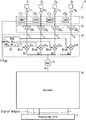
- a capacitive sensing system 100 comprises a sensor array 1 and a semiconductor device 2 .
- the sensor array 1 comprises sensing electrodes 3 arrayed in rows and columns.
- the sensor array 1 may be integrated in a touch panel.
- the sensor array 1 may be integrated in a display panel, such as a liquid crystal display (LCD) panel and an organic light emitting diode (OLED) display panel.
- LCD liquid crystal display
- OLED organic light emitting diode
- the common electrodes may be used as the sensing electrodes 3 , in one or more embodiments.
- the sensing electrodes 3 are connected to the semiconductor device 2 .
- the semiconductor device 2 comprises capacitive sensing circuitry 4 and a processing unit 5 .
- the capacitive sensing circuitry 4 is configured to obtain sensing signals having signal levels corresponding to capacitances of the sensing electrodes 3 and generate digital outputs based on the sensing signals.
- the processing unit 5 is configured to perform arithmetic processing on the digital outputs received from the capacitive sensing circuitry 4 to achieve proximity sensing of an object, such as a user's finger and a stylus, to the sensor array 1 .
- the arithmetic processing for the proximity sensing is performed in units of Q sensing electrodes arrayed in a specific direction, for example, the vertical direction in FIG. 1 , where Q is an integer of three or more.
- display driver circuitry configured to drive the display panel may be integrated in the semiconductor device 2 .
- the capacitive sensing circuitry 4 comprises input terminals 11 1 to 11 Q connected to the sensing electrodes 3 1 to 3 Q , respectively, driver circuitry 12 , current conveyer circuitry 13 , encoder circuitry 14 , an analog-digital (AD) converter 15 , and decoder circuitry 16 . Illustrated in FIG. 2 is the configuration of a part of the capacitive sensing circuitry 4 related to the Q sensing electrodes 3 enclosed in the dotted box 6 in FIG. 1 . In one or more embodiments, the Q sensing electrodes 3 illustrated in FIG. 2 are arrayed in the vertical direction in FIG. 1 . In one or more embodiments, one AD converter 15 is prepared for Q sensing electrodes 3 .
- the driver circuitry 12 comprises Q drivers 21 1 to 21 Q connected to the input terminals 11 1 to 11 Q , respectively.
- the drivers 21 1 to 21 Q are configured to supply drive signals to the sensing electrodes 3 1 to 3 Q , respectively.
- the drive signals are periodic signals of a frequency of f REF .
- the drivers 21 1 to 21 Q are supplied with a reference clock signal CLK REF of the frequency f REF , and configured to generate the drive signals in synchronization with the reference clock signal CLK REF .
- Signals of various waveforms may be used as the drive signals. For example, signals of a sinusoidal, triangular, or rectangular waveform may be used as the drive signals.
- the current conveyer circuitry 13 comprises current conveyers 22 1 to 22 Q connected to the input terminals 11 1 to 11 Q , respectively.
- the current conveyers 22 1 to 22 Q are configured to output sensing signals f 1 to f Q having signal levels corresponding to current levels of charging and discharging currents of the sensing electrodes 3 1 to 3 Q , respectively.
- the charging and discharging currents of the sensing electrodes 3 1 to 3 Q depend on the self-capacitances of the sensing electrodes 3 1 to 3 Q when the drive signals are supplied to the sensing electrodes 3 1 to 3 Q , and the sensing signals f 1 to f Q are obtained as signals generated by modulating the periodic signals of the frequency f REF with information of the self-capacitances of the sensing electrodes 3 1 to 3 Q .
- the encoder circuitry 14 comprises a phase shifter 23 and Q mixers 24 1 to 24 Q .
- the phase shifter 23 is configured to supply carrier waves Mix1 to MixQ to the mixers 24 1 to 24 Q , respectively, in synchronization with the reference clock signal CLK REF .
- the mixers 24 1 to 24 Q are configured to generate mixer outputs g 1 to g Q by modulating the carrier waves Mix1 to MixQ with the sensing signals f 1 to f Q , respectively.
- the carrier waves Mix1 to MixQ are each selected from signals ⁇ ⁇ /2 , ⁇ 0 , ⁇ ⁇ /2 , and ⁇ ⁇ .
- the signal ⁇ 0 is a signal in phase with the drive signals.
- the signal ⁇ 0 is a periodic signal having the same phase as that of the current waveforms of the drive signals.
- the signal ⁇ ⁇ is a signal of the opposite phase to that of the drive signals.
- the signal ⁇ ⁇ /2 is a periodic signal having a phase delayed from that of the signal ⁇ 0 by ⁇ /2
- the signal ⁇ ⁇ /2 is a periodic signal having a phase advanced from that of the signal ⁇ 0 by ⁇ /2, that is, a phase delayed from that of the signal ⁇ 0 by 3 ⁇ /2.
- a sum signal of the mixer outputs g 1 to g Q outputted from the mixers 24 1 to 24 Q is supplied to the AD converter 15 .
- the mixer outputs g 1 to g Q are current signals, and the outputs of the mixer 24 1 to 24 Q are commonly connected to the input of the AD converter 15 to achieve the addition of the mixer outputs g 1 to g Q through wired-sum.
- FIG. 2 illustrates such a configuration.
- the mixer output g k outputted from the mixer 24 k comprises information of an effective signal component for proximity sensing, in one or more embodiments.
- the mixer output g k comprises information of a noise component, in one or more embodiments.
- the signal level of the mixer output g k is originally expected to be zero, when the carrier wave Mixk is selected from the signals ⁇ ⁇ /2 and ⁇ ⁇ /2 , in one or more embodiments.
- the mixer output g k may be used for noise detection, when the carrier wave Mixk is selected from the signals ⁇ ⁇ /2 and ⁇ ⁇ /2 .
- a periodic signal of a different phase from that of the signals ⁇ 0 and ⁇ ⁇ may be used in place of the signal ⁇ ⁇ /2 or ⁇ ⁇ /2 .
- the signal level of the mixer output g k incorporates information of a noise component when a periodic signal of a different phase from that of the signals ⁇ 0 and ⁇ ⁇ is used as the carrier wave Mixk. Also in this case, the mixer output g k may be used for noise detection.
- the configuration of the encoder circuitry 14 achieves code division multiplexing.
- codes are assigned to the sensing signals f 1 to f Q .
- the phase shifter 23 is configured to select the carrier wave Mixk from among the signals ⁇ ⁇ /2 , ⁇ 0 , ⁇ ⁇ /2 and ⁇ ⁇ based on the code assigned to the sensing signal f k and supply the selected carrier wave Mixk to the mixer 24 k .
- the AD converter 15 is configured to perform analog-digital conversion on the sum signal of the mixer outputs g 1 to g Q received from the mixers 24 1 to 24 Q to output a digital data stream q.
- the decoder circuitry 16 constitutes processing circuitry configured to process the output of the AD converter 15 , that is, the digital data stream q, together with the processing unit 5 . In one or more embodiments, the decoder circuitry 16 is configured to decode the digital data stream q received from the AD converter 15 to generate the digital outputs. In one or more embodiments, the decoder circuitry 16 is configured to perform a product-sum operation to generate the digital outputs. In one or more embodiments, the processing unit 5 is configured to perform arithmetic processing on the digital outputs from the decoder circuitry 16 to achieve proximity sensing of an object to the sensor array 1 . In one or more embodiments, this arithmetic processing may comprise processing for detecting the position at which the object approaches or is in contact with the sensor array 1 .
- Q is an even number of four or more.
- Q can be represented as 2N, where N is an integer of two or more. It should be noted that the technologies of this disclosure are applicable to a case where Q is an odd number of three or more, as described later.
- each sensing frame comprises Q bursts, that is, 2N bursts.
- the 2N bursts may be referred to as bursts #1 to #(2N), respectively.
- the drivers 21 1 to 21 2N are configured to continue outputting drive signals over bursts #1 to #(2N) with a constant waveform.
- the waveform of the sensing signal f i is expected to remain unchanged over bursts #1 to #(2N), and therefore the waveform of the mixer output g i outputted from the mixer 24 i is also expected to remain unchanged over bursts #1 to #(2N). It is therefore expected that the following expressions (1) hold:
- t+(2N ⁇ 1)T are the times when the AD converter 15 samples the input signal during burst #1 to #(2N), respectively, and A 1 (t) to A 2N (t) are the signal levels of the sensing signals f 1 to f 2N at time t.
- the signal levels of the sensing signals f 1 to f 2N at times t, t+T . . . and t+(2N ⁇ 1) may be simply referred to as A 1 to A 2N .
- the signal levels on the inputs of the encoder circuitry 14 that is, the signal levels of the sensing signals f 1 to f 2N may be collectively represented by an input tensor a, which is represented by the following expression (2):
- the processing performed by the encoder circuitry 14 during bursts #1 to #(2N) can be expressed as an encode tensor E defined by the following expression (3):
- the digital data stream q outputted from the AD converter 15 can be represented by the following expression (4):
- the sum signal supplied to the AD converter 15 and the digital data stream q outputted from the AD converter 15 comprise information of a signal component of the sensing signal f k effective for proximity sensing during the certain burst.
- the digital data stream q outputted from the AD converter 15 comprises information of a noise component of the sensing signal f k during the certain burst, in place of the component of the sensing signal f k effective for proximity sensing.
- the digital outputs of the decoder circuitry 16 are represented by an output tensor b x .
- the decode tensor X can demodulate the input tensor a modulated with the encode tensor E when the product XE of the encode tensor E and the decode tensor X recited in expression (5) has only one non-zero element in each row.
- each of the carrier wave Mix1 to Mix(2N) is selected from the signals ⁇ 0 and ⁇ ⁇ during two or more of bursts #1 to #(2N) to suppress detection of a motion artifact.
- this operation increases the number of sampling of information of effective signal components for proximity sensing per each sensing frame with a reduced number of the AD converter 15 , while effectively suppressing detection of a motion artifact.
- information of effective signal components for proximity sensing are sampled a plurality of times in each sensing frame, and this allows increasing an effective sampling frequency, suppressing detection of a motion artifact.
- each of the carrier waves Mix1 to Mix(2N) is selected from the signals ⁇ 0 and ⁇ ⁇ during two of more of the bursts #1 to #(2N), and accordingly there are two or more real elements in each column of the encode tensor E.
- the product XE of the encode tensor E and the decode tensor X has one non-zero element in each row under such restriction, due to appropriate selection of the encode tensor E and the decode tensor X.
- such selection of the encode tensor E and the decode tensor X is achieved through appropriate selection of the carrier waves Mix1 to Mix(2N) in the encoder circuitry 14 and appropriate design of the matrix operation performed in the decoder circuitry 16 .
- the sampling timing of effective signal components for proximity sensing is evenly distributed in the time domain.
- bursts in which the carrier wave Mixk, which is modulated with the sensing signal f k , is selected from the signals ⁇ 0 and ⁇ ⁇ may be selected so that the selected bursts are not adjacent to each other in the time domain.
- bursts in which the carrier wave Mixk is selected from the signals ⁇ 0 and ⁇ ⁇ and bursts in which the carrier wave Mixk is selected from the signals ⁇ ⁇ /2 and ⁇ ⁇ /2 may be alternately disposed. This operation may effectively suppress detection of a motion artifact.
- sensing electrodes 3 from which information of effective signal components for proximity sensing may be spatially evenly distributed.
- one of the carrier waves Mix(2p ⁇ 1) and Mix(2p) is selected from the signals ⁇ 0 and ⁇ ⁇ in a burst in which the other is selected from the signals ⁇ ⁇ /2 and ⁇ ⁇ /2 . This operation may effectively suppress detection of a motion artifact.
- the noise detection may be achieved based on mixer outputs obtained by modulating the signal ⁇ ⁇ /2 or ⁇ ⁇ /2 with the sensing signals f 1 to f Q .
- the decoder circuitry 16 is designed to extract a noise component generated by modulating the signal ⁇ ⁇ /2 or ⁇ ⁇ /2 with the sensing signals f 1 to f Q .
- the timing at which information of noise components is obtained is evenly distributed in the time domain.
- bursts in which the carrier wave Mixk, which is modulated with each sensing signal f k , is selected from the signals ⁇ ⁇ /2 and ⁇ ⁇ /2 are selected from bursts #1 to #(2N) so that the selected bursts are not adjacent in the time domain.
- the carrier wave Mixk is selected from the signals ⁇ ⁇ /2 and ⁇ ⁇ /2 in every one burst.
- the timing of obtaining the noise components may be spatially evenly distributed.
- one of the carrier waves Mix(2p ⁇ 1) and Mix(2p) is selected from the signals ⁇ 0 and ⁇ ⁇ in a burst in which the other is selected from the signals ⁇ ⁇ /2 and ⁇ ⁇ /2 .
- the above-described conditions in which timing and positions for obtaining information of effective signal components and information of the noise components are evenly distributed can be described with an encode tensor E in which elements of real numbers and elements of pure imaginary numbers are arranged in a checkered pattern.
- the encode tensor E can be represented by the following expression (6a) with two encode matrices E 1 and E 2 represented by the following expressions (6b) and (6c), in one or more embodiments:
- E E 1 + iE 2 , ( 6 ⁇ a )
- E 1 ( e 11 0 ... e 1 ⁇ ( 2 ⁇ N - 1 ) 0 0 e 22 0 e 2 ⁇ ( 2 ⁇ N ) ⁇ ⁇ ⁇ e ( 2 ⁇ N - 1 ) ⁇ 1 0 e ( 2 ⁇ N - 1 ) ⁇ ( 2 ⁇ N - 1 ) 0 0 e ( 2 ⁇ N ) ⁇ 2 ... ⁇ 0 e ( 2 ⁇ N ) ⁇ ( 2 ⁇ N ) ) , ⁇ and ( 6 ⁇ b )
- E 2 ( 0 e 12 ... 0 e 1 ⁇ ( 2 ⁇ N ) e 21 0 e 2 ⁇ ( 2 ⁇ N - 1 ) 0 ⁇ ⁇ ⁇ 0 e ( 2 ⁇ N - 1 ) ⁇ 2 0 e ( 2 ⁇ N - 1 )
- the encode matrices E 1 and E 2 can be represented by the following expressions (7a) and (7b) for a case where N is two, that is, the number of the sensing electrodes 3 for one AD converter 15 is four:
- E 1 ( e 11 0 e 13 0 0 e 22 0 e 24 e 31 0 e 33 0 0 e 42 0 e 44 )
- E 2 ( 0 e 12 0 e 14 e 21 0 e 23 0 0 e 32 0 e 34 e 41 0 e 43 0 ) .
- 7 ⁇ b
- a 2 ⁇ 2 matrix O kl in which one element is 1 and the remaining elements are 0 is defined by the following expression (8):
- O kl ⁇ ik ⁇ jl ⁇ , (8) where ⁇ ij is the Kronecker delta.
- the matrices O 11 , O 22 , O 12 , and O 21 are represented by the following expressions (9a) to (9d):
- the encode matrices E 1 and E 2 can be represented with the partial matrix e kl and the matrix O kl by the following expressions (11a) and (11b):
- the encode matrices E 1 and E 2 can be represented by the following expressions (12a) and (12b) for a case where N is two, that is, the number of the sensing electrodes 3 for one AD converter 15 is four:
- E 1 ( e 11 e 13 e 31 e 33 ) ⁇ ( 1 0 0 0 ) + ( e 22 e 24 e 42 e 44 ) ⁇ ( 0 0 0 1 )
- E 2 ( e 12 e 14 e 32 e 34 ) ⁇ ( 0 1 0 0 ) + ( e 21 e 23 e 41 e 43 ) ⁇ ( 0 0 1 0 ) .
- the partial matrices e 11 and e 22 of the encode matrix E 1 and the partial matrices e 12 and e 21 of the encode matrix E 2 are 2 ⁇ 2 matrices, and it would be understood that expressions (11a) and (11b) hold for N being 2 when these partial matrices are defined by the following expressions (13a) to (13d):
- the encode tensor E is represented by the following expression (14):
- the decode tensor X is represented by the following expression (15):
- the output tensor b x is represented by the following expression (16), in one or more embodiments:
- M is selected as being 2.
- matrices V 1 and V 2 are selected as basic linear transformations for expression (14)
- matrices W 1 and W 2 are selected as basic linear transformations for expression (15), where the matrices V 1 and V 2 are orthogonal to each other, and the matrices W 1 and W 2 are orthogonal to each other.
- the product XE of the encode tensor E and the decode tensor X is represented by the following expression (17):
- the decode tensor X can decode the input tensor a modulated with the encode tensor E when the product XE, which is represented by expression (17), has only one non-zero element in each row.
- the decode matrices X 1 and X 2 can be represented by the following expressions (18) and (19) with the matrix O kl :
- the product XE of the encode tensor E and the decode tensor X has only one non-zero element in each row, allowing demodulation of the input tensor a.
- the input tensor a is reproduced as the output tensor b x through selecting the partial matrices of the encode matrices E 1 and E 2 and the decode matrices X 1 and X 2 so as to satisfy the above-described expressions (23), (24a) and (24b). In one or more embodiments, this allows obtaining information of the signal levels A 1 to A 2N of the sensing signals f 1 to f 2N as the digital outputs of the decode circuitry 16 .
- the solution space of the eight equations (22) is narrowed by adding constraint conditions.
- the circuit size of the decoder circuitry 16 is additionally reduced by appropriately defining the constraint conditions.
- the decode matrices are selected so that two or more different basic linear transformations do not appear in each column, and thereby the number of linear transformation circuits simultaneously operate in the decoder circuitry 16 is reduced to one. This is advantageous in terms of the circuit size and the control logic size.
- variable matrices related to the decode matrices X 1 and X 2 are degenerated by using matrices X 1a and X 2a as the decode matrices X 1 and X 2 so that only four matrices x 11 , x 21 , y 12 , and y 22 are variable matrices, where the matrix X 1a is defined so that the elements in the even columns are zero as recited in expression (25), and the matrix X 2a is defined so that the elements in the odd columns are zero as recited in expression (26):
- X 2 ⁇ ⁇ a ( 0 y 12 0 y 1 ⁇ ( 2 ⁇ ⁇ N ) ... 0 y 22 0 y 2 ⁇ ( 2 ⁇ N ) ⁇ ⁇ 0 y ( 2 ⁇ N - 1 )
- the condition to reproduce the input tensor a that is, the condition that the product XE of the encode tensor E and the decode tensor X has only one non-zero element in each row
- x 11 e 11 +y 12 e 21 c 1 ⁇ 1g I
- ⁇ y 12 e 22 +x 11 e 12 c 2 ⁇ 2g I
- x 21 e 11 +y 22 e 21 c 3 ⁇ 2g I
- ⁇ y 22 e 22 +x 21 e 12 c 4 ⁇ 1g I
- I is the unit matrix
- c 1 , c 2 , c 3 , and c 4 are arbitrary constants
- g is an integer of 1 or 2. This is based on the fact that, if a plurality of non-zero elements appear in the same row of the matrices corresponding to the basic linear transformations V 1 and V 2 , this
- variable matrices related the decode matrices X 1 and X 2 are degenerated by using matrices X 1b and X 2b as the decode matrices X 1 and X 2 so that only four matrices x 12 , x 22 , y 11 , and y 21 are variable matrices, where the matrix X 1b is defined so that the elements in the odd columns are zero as recited in expression (30) and the matrix X 2b is defined so that the elements in the even columns are zero as recited in expression (31):
- X 2 ⁇ b ( y 11 0 y 1 ⁇ ( 2 ⁇ ⁇ N - 1 ) 0 ... y 21 0 y 2 ⁇ ( 2 ⁇ N - 1 ) 0 ⁇ ⁇ ⁇ y ( 2 ⁇ N - 1 ) ⁇ 1 0 y ( 2 ⁇
- the condition to demodulate the input tensor a that is, the condition that the product XE of the encode tensor E and the decode tensor X has only one non-zero element in each row
- ⁇ y 11 e 11 +x 12 e 21 c 5 ⁇ 1g I
- x 12 e 22 +y 11 e 12 c 6 ⁇ 2g I
- ⁇ y 21 e 11 +x 22 e 21 c 7 ⁇ 2g I
- x 22 e 22 +y 21 e 12 c 8 ⁇ 1g I.
- the encoder circuitry 14 is designed to select the carrier waves Mix1 to Mix(2N) based on the encode tensor E of the obtained solution, and the decoder circuitry 16 is designed to perform product-sum operations in accordance with the decode tensor X of the obtained solution.
- the values q 1 to q 2N of the digital data stream q outputted from the AD converter 15 which are represented by expression (4), incorporate information of noise components as well as information of the effective signal components, where the effective signal components correspond to information generated by modulating the signals ⁇ 0 and ⁇ 90 with the sensing signal f 1 to f 2N , and the noise components correspond to information generated by modulating the signals ⁇ ⁇ /2 and ⁇ ⁇ /2 with the sensing signal f 1 to f 2N .
- noise detection may be achieved by designing the decoder circuitry 16 to extract information generated by modulating the signals ⁇ ⁇ /2 and ⁇ ⁇ /2 with the sensing signals f 1 to f 2N .
- the decode matrix X a is applied to the digital data stream q to obtain the output tensor b x so that odd elements thereof correspond to information generated by modulating the signal ⁇ 0 or ⁇ ⁇ with the sensing signals f 1 to f 2N , that is, information of effective signal components, and even elements thereof correspond to information generated by modulating the signal ⁇ ⁇ /2 or ⁇ ⁇ /2 with the sensing signals f 1 to f 2N , that is, information of noise components.
- the decode matrix X b is applied to the digital data stream q to obtain the output tensor b x so that odd elements thereof correspond to information of noise components, and even elements thereof correspond to information of effective signal components.
- the decode matrices X a and X b are applied to the digital data stream q outputted from the AD converter 15 in the decoder circuitry 16 to obtain digital outputs corresponding to the effective signal components and digital outputs corresponding to the noise components.
- the processing unit 5 may be configured to achieve proximity sensing based on the digital outputs corresponding to the effective signal components and achieve noise detection based on the digital outputs corresponding to the noise components. In one or more embodiments, when detecting existence of noise based on the digital outputs corresponding to the noise components in a sensing frame, the processing unit 5 may discard data of the digital outputs corresponding to the effective signal components obtained for this sensing frame. In such an embodiment, proximity sensing of an object to the sensor array 1 may be achieved based on the digital outputs corresponding to the effective signal components obtained in a sensing frame for which no noise is detected.
- the above-described techniques of this disclosure is applicable to a case where Q is an odd number of three or more, for example, a case where Q is 2N ⁇ 1 for N being an integer of two or more.
- a similar calculation to that described above is performed with an assumption that the signal level A 2N of the sensing signal f 2N is zero during all of bursts #1 to #(2N), in one or more embodiments.
- the calculation result with respect to the sensing signal f 2N is discarded in the decoder circuitry 16 .
- the encode tensor E is a 4 ⁇ 4 matrix and the encode matrices E 1 and E 2 are represented by expressions (7a) and (7b), in one or more embodiments.
- the partial matrices e 11 , e 12 , e 21 , and e 22 of the encode matrices E 1 and E 2 are all 2 ⁇ 2 matrices.
- all of the elements of the encoder matrices E 1 and E 2 are selected from +1 or ⁇ 1 to eliminate a need for providing a variable gain stage for the encoder circuitry 14 . This may be advantageous in terms of the circuit size. In one or more embodiments, a similar approach may be applied to the decode matrices X 1 and X 2 and the decoder circuitry 16 .
- the partial matrices e 11 , e 12 , e 21 , and e 22 of the encode matrices E 1 and E 2 , the partial matrices x 11 , x 21 , x 12 , and x 22 of the decode matrix X 1 , and the partial matrices y 11 , y 21 , y 12 , and y 22 of the decode matrix X 2 are selected from 16 2 ⁇ 2 matrices defined by the following expressions (36):
- the partial matrices of the encode matrices and the decode matrices are all defined as being regular to simplify the calculation; this allows handling the partial matrices of the decode matrices as integer multiples of the inverse matrices of the partial matrices of the encode matrices.
- the solution space is accordingly restricted in accordance with the following expressions (37) and (38): e kl ⁇ M 4 , ⁇ M 5 , ⁇ M 6 , ⁇ M 7 ⁇ , (37) x kl ⁇ M 4 , ⁇ M 5 , ⁇ M 6 , ⁇ M 7 ⁇ , and y kl ⁇ M 4 , ⁇ M 5 , ⁇ M 6 , ⁇ M 7 ⁇ .
- the solution space is restricted in accordance with expressions (37) and (38).
- a sum or difference of two matrix products becomes an integer multiple of the unit matrix only when the two matrix products are each an integer multiple of the unit matrix.
- coefficients of 2 appear in expressions (43), because partial matrices of the decode matrices have coefficients of 2, when the partial matrices of the decode matrices are integer multiples of the partial matrices of the encode matrices.
- a solution is obtained by searching two pairs of regular 2 ⁇ 2 matrices for which the matrix products are equal to each other. In one or more embodiments, there is a plurality of pairs satisfying this requirement.
- ⁇ M 4 ⁇ ( 0 1 1 0 ) ⁇ M 6
- ⁇ ⁇ M 4 ⁇ ( 0 - 1 1 0 ) ⁇ M 5
- the encode tensor E and the decode matrices X a and X b can be represented by the following expressions (50) and (51), in one or more embodiments:
- the products of the decode matrices X a and X b and the encode tensor E can be represented by the following expression (52):
- the decoder circuitry 16 comprises a digital demodulator 25 , coefficient supplying circuitry 26 , decimeter/filters 27 and 28 , and a decoder 29 .
- the digital demodulator 25 is configured to demodulate the digital data stream q with an in-phase local carrier which is in phase with the drive signals and an out-of-phase local carrier having a phase shifted from that of the in-phase local carrier by ⁇ /2.
- the digital demodulator 25 comprises digital mixers 31 and 32 .
- the digital mixer 31 is configured to multiply the digital data stream q by coefficients ⁇ 0 corresponding to the in-phase local carrier
- the digital mixer 32 is configured to multiply the digital data stream q by coefficients ⁇ ⁇ /2 corresponding to the out-of-phase local carrier, which has a phase delayed from that of the in-phase local carrier by ⁇ /2.
- the coefficient supplying circuitry 26 is configured to supply the coefficients ⁇ 0 to the digital mixer 31 and the coefficients ⁇ ⁇ /2 to the digital mixer 32 , in synchronization with a reference clock signal CLK REF .
- the decoder 29 comprises product-sum operation circuitries 33 and 34 .
- the product-sum operation circuitry 33 is configured to perform a product-sum operation corresponding to the decode matrix X a
- the product-sum operation circuitry 34 is configured to perform a product-sum operation corresponding to the decode matrix X b .
- the decimeter/filter 27 is configured to distribute the output of the digital mixer 31 to the product-sum operation circuitries 33 and 34
- the decimeter/filter 28 is configured to distribute the output of the digital mixer 32 to the product-sum operation circuitries 33 and 34 .
- the mixers 24 1 to 24 4 use the signals ⁇ 0 , ⁇ ⁇ /2 , ⁇ 0 , and ⁇ ⁇ /2 as the carrier waves Mix1 to Mix4, respectively, and modulate the carrier waves Mix1 to Mix4 with the sensing signals f 1 to f 4 , respectively, during burst #1.
- this operation corresponds to the first row of the encode matrices E 1 and E 2 in equation (50).
- the digital mixers 31 and 32 outputs demodulated data B 1 . 1 and B 1 . 2 obtained by multiplying q 1 by the coefficients ⁇ 0 and ⁇ ⁇ /2 , respectively.
- the demodulated data B 1 . 1 and B 1 .
- the decimeter/filter 27 outputs the demodulated data B 1 . 1 received from the digital mixer 31 to the product-sum operation circuitry 33
- the decimeter/filter 28 outputs the demodulated data B 1 . 2 received from the digital mixer 32 to the product-sum operation circuitry 34 .
- the mixers 24 1 to 24 4 use the signals ⁇ ⁇ /2 , ⁇ 0 , ⁇ ⁇ /2 , and ⁇ 0 as the carrier waves Mix1 to Mix4, respectively, and modulate the carrier waves Mix1 to Mix4 with the sensing signals f 1 to f 4 , respectively, during burst #2.
- this operation corresponds to the second row of the encode matrices E 1 and E 2 in equation (50).
- the digital mixers 31 and 32 outputs demodulated data B 2 . 1 and B 2 . 2 obtained by multiplying q 2 by the coefficients ⁇ 0 and ⁇ ⁇ /2 , respectively.
- the demodulated data B 2 . 1 and B 2 .
- the decimeter/filter 27 outputs the demodulated data B 2 . 1 received from the digital mixer 31 to the product-sum operation circuitry 34
- the decimeter/filter 28 outputs the demodulated data B 2 . 2 received from the digital mixer 32 to the product-sum operation circuitry 33 .
- the mixers 24 1 to 24 4 use the signals ⁇ 0 , ⁇ ⁇ /2 , ⁇ 0 , and ⁇ ⁇ /2 as the carrier waves Mix1 to Mix4, respectively, and modulate the carrier waves Mix1 to Mix4 with the sensing signals f 1 to f 4 , respectively, during burst #3.
- this operation corresponds to the third row of the encode matrices E 1 and E 2 in equation (50).
- the digital mixers 31 and 32 output demodulated data B 3 . 1 and B 3 . 2 obtained by multiplying q 3 by the coefficients ⁇ 0 and ⁇ ⁇ /2 , respectively.
- the demodulated data B 3 . 1 and B 3 are examples of the digital data stream q outputted from the AD converter 15 during burst #3.
- the decimeter/filter 27 outputs the demodulated data B 3 . 1 received from the digital mixer 31 to the product-sum operation circuitry 33
- the decimeter/filter 28 outputs the demodulated data B 3 . 2 received from the digital mixer 32 to the product-sum operation circuitry 34 .
- the mixers 24 1 to 24 4 use the signals ⁇ ⁇ /2 , ⁇ 0 , ⁇ ⁇ /2 , and ⁇ 0 as the carrier waves Mix1 to Mix4, respectively, and modulate the carrier waves Mix1 to Mix4 with the sensing signals f 1 to f 4 , respectively, during burst #4.
- this operation corresponds to the fourth row of the encode matrices E 1 and E 2 in equation (50).
- the digital mixers 31 and 32 outputs demodulated data B 4 . 1 and B 4 . 2 obtained by multiplying q 4 by the coefficients ⁇ 0 and ⁇ ⁇ /2 , respectively.
- the decimeter/filter 27 outputs the demodulated data B 4 . 1 received from the digital mixer 31 to the product-sum operation circuitry 34
- the decimeter/filter 28 outputs the demodulated data B 4 . 2 received from the digital mixer 32 to the product-sum operation circuitry 33 .
- the product-sum operation circuitries 33 and 34 of the decoder 29 performs operations corresponding to the decode matrices X a and X b on the data B 1 . 1 to B 4 . 1 and B 1 . 2 to B 4 . 2 received from the decimeter/filters 27 and 28 during bursts #1 to #4 to calculate digital outputs 4A 1 ⁇ 0 , 4A 2 ⁇ 0 , 4A 3 ⁇ 0 , and 4A 4 ⁇ 0 , which correspond to effective signal components, and digital outputs 4A 1 ⁇ ⁇ /2 , 4A 2 ⁇ ⁇ /2 , 4A 3 ⁇ ⁇ /2 , and 4A 4 ⁇ ⁇ /2 , which correspond to noise components.
- the decode matrices X a and X b recites the unit imaginary number i, and accordingly the product-sum operation circuitries 33 and 34 are configured to use values outputted from the digital mixer 32 in performing multiplication by the unit imaginary number i; the product-sum operation circuitries 33 and 34 themselves are configured to perform operations in the real number domain, in one or more embodiments.
- the product-sum operation circuitry 33 calculates the digital outputs 4A 1 ⁇ 0 , 4A 2 ⁇ ⁇ /2 , 4A 3 ⁇ 0 , and 4A 4 ⁇ ⁇ /2 by performing a matrix operation on the demodulated data B 1 . 1 , B 2 . 2 , B 3 . 1 , and B 4 . 2 received during bursts #1 to #4, in accordance with the following expression (61):
- the product-sum operation circuitry 34 calculates the digital outputs 4A 1 ⁇ ⁇ /2 , 4A 2 ⁇ 0 , 4A 3 ⁇ ⁇ /2 , and 4A 4 ⁇ 0 by performing a matrix operation on the demodulated data B 1 . 2 , B 2 . 1 , B 3 . 2 , and B 4 . 1 received during bursts #1 to #4, in accordance with the following expression (62):
- the processing unit 5 is configured to perform arithmetic processing for proximity sensing of an object to the sensor array 1 , based on the digital outputs 4A 1 ⁇ 0 , 4A 2 ⁇ 0 , 4A 3 ⁇ 0 , and 4A 4 ⁇ 0 , which correspond to the effective signal components.
- the processing unit 5 is further configured to perform noise detection based on the digital outputs 4A 1 ⁇ ⁇ /2 , 4A 2 ⁇ ⁇ /2 , 4A 3 ⁇ ⁇ /2 , and 4A 4 ⁇ ⁇ /2 , which correspond to the noise components.
- the digital outputs 4A 1 ⁇ ⁇ /2 , 4A 2 ⁇ ⁇ /2 , 4A 3 ⁇ ⁇ /2 , and 4A 4 ⁇ ⁇ /2 are expected to be zero, in one or more embodiments. If not so, the sensing signals f 1 to f 4 are determined as experiencing an influence of noise.
- the sensor array 1 further comprises drive electrodes opposed to the sensing electrodes 3 1 to 3 Q , in one or more embodiments.
- the driver circuitry 12 is configured to supply drive signals to the drive electrodes opposed to the sensing electrodes 3 1 to 3 Q .
- FIG. 1 illustrates the arrangement in which sensing electrodes 3 associated with one AD converter 15 are arrayed in the vertical direction
- the arrangement of sensing electrodes 3 associated with one AD converter 15 may be variously modified.
- FIG. 9 for example, when sensing electrodes 3 are grouped into Q groups 40 1 to 40 Q arrayed in a specific direction, in the horizontal direction in FIG. 9 , Q sensing electrodes 3 belonging to different groups 40 may be selected as sensing electrodes 3 associated with one AD converters 15 .
- the sensing electrodes 3 indicated by the hatchings in FIG. 9 may be selected as sensing electrodes 3 associated with one AD converters 15 .
Landscapes
- Engineering & Computer Science (AREA)
- General Engineering & Computer Science (AREA)
- Theoretical Computer Science (AREA)
- Human Computer Interaction (AREA)
- Physics & Mathematics (AREA)
- General Physics & Mathematics (AREA)
- Transmission And Conversion Of Sensor Element Output (AREA)
- Measurement Of Length, Angles, Or The Like Using Electric Or Magnetic Means (AREA)
Abstract
Description
where t, t+T, . . . and t+(2N−1)T are the times when the
where the jth row of the encode tensor E represents the processing performed during burst #j by the
-
- where q1 to q2N are the values of the digital data stream q during
bursts # 1 to #(2N), respectively.
- where q1 to q2N are the values of the digital data stream q during
bX=XEa, (5)
where X is a decode tensor which represents matrix operations performed on the digital data stream q by the
where the element eij of the encode matrix E1 is a non-zero real number for i+j being an even number, and zero for i+j being an odd number, while the element eij of the encode matrix E2 is zero for i+j being an even number, and a non-zero real number for i+j being an odd number.
O kl={δikδjl}, (8)
where δij is the Kronecker delta. In one or more embodiments, the matrices O11, O22, O12, and O21 are represented by the following expressions (9a) to (9d):
e kl={e (k+2(i−2))(l+(2j−1))}, (10)
where the partial matrix ekl is an N×N matrix.
where the operator ⊗ is the Kronecker product.
In one or more embodiments, the partial matrices e11 and e22 of the encode matrix E1 and the partial matrices e12 and e21 of the encode matrix E2 are 2×2 matrices, and it would be understood that expressions (11a) and (11b) hold for N being 2 when these partial matrices are defined by the following expressions (13a) to (13d):
where the encode matrix Em corresponds to a basic linear transformation Vm.
where the decode matrix Xm corresponds to a basic linear transformation Wm.
In one or more embodiments, the decode tensor X can decode the input tensor a modulated with the encode tensor E when the product XE, which is represented by expression (17), has only one non-zero element in each row.
where the matrices x11, x12, x21, and x22 in expressions (18) are partial matrices of the decode matrix X1, and the matrices y11, y12, y21, and y22 in expressions (19) are partial matrices of the decode matrix X2.
X 1 E 1 +X 2 E 2=(x 11 e 11)⊗O 11+(x 12 e 22)⊗O 12+(x 21 e 11)⊗O 21+(x 22 e 22)⊗O 22+(y 12 e 21)⊗O 11+(y 11 e 12)⊗O 12+(y 22 e 21)⊗O 21+(y 21 e 12)⊗O 22=(x 11 e 11 +y 12 e 21)⊗O 11+(x 12 e 22 y 11 e 12)⊗O 12+(x 21 e 11 +y 22 e 21)⊗O 21+(x 22 e 22 +y 21 e 12)⊗O 22, and (20)
−X 2 E 1 +X 1 E 2=(−y 11 e 11 +x 12 e 21)⊗O 11+(−y 12 e 22 +x 11 e 12)⊗O 12+(−y 21 e 11 +x 22 e 21)⊗O 21+(−y 22 e 22 x 21 e 12)⊗O 22. (21)
x 11 e 11 +y 12 e 21 =c 1δ1g O 11 +c 2δ1g′ O 22,
x 12 e 22 +y 11 e 12 =c 3δ2g O 11 +c 4δ2g′ O 22,
−y 11 e 11 +x 12 e 21 =c 5δ3g O 11 +c 6δ3g′ O 22,
−y 12 e 22 +x 11 e 12 =c 7δ4g O 11 +c gδ4g′ O 22,
x 21 e 11 +y 22 e 21 =c 9δ1h O 11 +c 10δ1h′ O 22,
x 22 e 22 +y 21 e 12 =c 11δ2h O 11 +c 12δ2h′ O 22,
−y 21 e 11 +x 22 e 21 =c 13δ3h O 11 +c 14δ3h′ O 22, and
−y 22 e 22 +x 21 e 12 =c 15δ4h O 11 +c 16δ4h′ O 22, (22)
where c1 to c16 are arbitrary constants, and g, g′, h, and h′ are any integer from one to four.
e11=e12=e21=e22=e, (23)
and the following expressions (24a) and (24b) hold for the partial matrices x11, x12, x21, and x22 of the decode matrix X1 and the partial matrices y11, y12, y21 and y22 of the decode matrix X2:
x 11 =y 12 =x 21 =−y 22=2(e)−1, and (24a)
−y 11 =x 12 =y 21 x 22=2(e)−1. (24b)
X 1a E 1 +X 2a E 2=(x 11 e 11 +y 12 e 21)⊗O 11+(x 21 e 11 +y 22 e 21)⊗O 21, and (27)
−X 2a E 1 +X 1a E 2=(−y 12 e 22 +x 11 e 12)⊗O 12+(−y 22 e 22 +x 21 e 12)⊗O 22. (28)
x 11 e 11 +y 12 e 21 =c 1δ1g I,
−y 12 e 22 +x 11 e 12 =c 2δ2g I,
x 21 e 11 +y 22 e 21 =c 3δ2g I, and
−y 22 e 22 +x 21 e 12 =c 4δ1g I, (29)
where I is the unit matrix, c1, c2, c3, and c4 are arbitrary constants, and g is an integer of 1 or 2. This is based on the fact that, if a plurality of non-zero elements appear in the same row of the matrices corresponding to the basic linear transformations V1 and V2, this is a valueless and redundant decode result.
X 1b E 1 +X 2b E 2=(x 12 e 22 +y 11 e 12)⊗O 12+(x 22 e 22 +y 21 e 12)⊗O 22, and (32)
−X 2b E 1 +X 1b E 2=(−y 11 e 11 +x 12 e 21)⊗O 11+(−y 21 e 11 +x 22 e 21)⊗O 21. (33)
−y 11 e 11 +x 12 e 21 =c 5δ1g I,
x 12 e 22 +y 11 e 12 =c 6δ2g I,
−y 21 e 11 +x 22 e 21 =c 7δ2g I, and
x 22 e 22 +y 21 e 12 =c 8δ1g I. (34)
X a =X 1a −iX 2a, and
X b =X 1b −iX 2b. (35)
e kl∈{±M 4 , ±M 5 , ±M 6 , ±M 7}, (37)
x kl∈{±M 4 , ±M 5 , ±M 6 , ±M 7}, and
y kl∈{±M 4 , ±M 5 , ±M 6 , ±M 7}. (38)
In one or more embodiments, the restriction of the solution space with respect to the partial matrices xkl and ykl of the decode matrices is based on the relations recited in expressions (39):
±M 4=±2(M 4)−1,
+M 5=±2(M 5)−1,
±M 6=±2(M 7)−1, and
⊥M 7=±2(M 6)−1, (39)
x 11 e 11 +y 12 e 21 =c 1δ1g I,
−y 12 e 22 +x 11 e 12 =c 2δ2g I,
x 21 e 11 +y 22 e 21 −c 3δ2g I,
−y 22 e 22 +x 21 e 12 =c 4δ1g I, (40)
e22=e21=e12=e11,
x 11 =y 12 =x 21=(e 11)−1, and
y 22=−(e 11)−1. (41)
x 11 e 11 +y 12 e 21 =c 1 I,
−y 12 e 22 +x 11 e 12=0,
x 12 e 11 +y 22 e 21=0,
−y 22 e 22 +x 21 e 12 =c 4 I,
−y 11 e 11 +x 12 e 21 =c 5 I,
x 12 e 22 +y 11 e 12=0,
−y 21 e 11 +x 22 e 21=0, and
x 22 e 22 +y 21 e 12 =c 8 I, (42)
x 11=2(e 11)−1,
−y 11=2(e 11)−1 =x 11,
x 12=2(e 21)−1,
y 12=2(e 21)−1 =x 12,
x 21=2(e 12)−1,
y 21=2(e 12)−1 =x 21,
x 22=2(e 22)−1,
y 22=2(e 22)−1 =x 22,
c1=4,
c2=4,
c3=4, and
c4=4. (43)
In one or more embodiments, coefficients of 2 appear in expressions (43), because partial matrices of the decode matrices have coefficients of 2, when the partial matrices of the decode matrices are integer multiples of the partial matrices of the encode matrices.
−y 12 e 22 +x 11 e 12=0,
x 21 e 11 +y 22 e 21=0,
x 12 e 22 +y 11 e 12=0, and
y 21 e 11 +x 22 e 21=0, (44)
because, when products of regular matrices are equal, the inverse matrices thereof are equal. In one or more embodiments, this equivalence is obtained from the following expressions (45) and (46):
x11e12−y12e22,
(x 11 e 12)−1=(y 12 e 22)−1,
(e 12)−1(x 11)−1=(e 22)−1(y 12)−1,
x 21 e 11 =−y 22 e 21, (45)
−y11=x11,
x12=y12,
y21=x21, and
x 22 =−y 22. (46)
In one or more embodiments, based on this equivalence, a solution is obtained by searching two pairs of regular 2×2 matrices for which the matrix products are equal to each other. In one or more embodiments, there is a plurality of pairs satisfying this requirement.
if one of the simplest solution representable by the following expression (48) is obtained, remaining solutions are readily obtained, in one or more embodiments:
ekl=M4. (48)
e11=M4,
e12=M5,
e21=M6,
e22=M7,
x11=M4,
y12=M7,
x21=M5,
−y 22 =M 6,
−y 11 =M 4,
x12=M7,
y21=M5, and
x22=M6, (49)
Expressions (49) represents one of solutions which allows demodulating the input tensor a.
q 1=(A 1 +A 3)Φ0−(A 2 −A 4)Φπ/2. (53)
In one or more embodiments, the
B1.1=(A 1 +A 3)Φ0−(A 2 −A 4)Φπ/2, and (54a)
B1.2=(A 1 +A 3)Φπ/2+(A 2 −A 4)Φ0. (54b)
In one or more embodiments, the decimeter/
q 2=(A 1 −A 3)Φπ/2+(A 2 +A 4)Φ0. (55)
In one or more embodiments, the
B2.1=(A 1 −A 3)Φπ/2+(A 2 +A 4)Φ0, and (56a)
B2.2=−(A 1 −A 3)Φ0+(A 2 +A 4)Φπ/2. (56b)
In one or more embodiments, the decimeter/
q 3=(A 1 −A 3)Φ0+(A 2 +A 4)Φπ/2. (57)
In one or more embodiments, the
B3.1=(A 1 −A 3)Φ0+(A 2 +A 4)Φπ/2, and (58a)
B3.2=(A 1 −A 3)Φπ/2−(A 2 +A 4)Φ0. (58b)
In one or more embodiments, the decimeter/
q 4=(A 1 +A 3)Φπ/2−(A 2 −A 4)Φ0. (59)
B4.1=(A 1 +A 3)Φπ/2−(A 2 −A 4)Φ0, and (60a)
B4.2=−(A 1 +A 3)Φ0−(A 2 −A 4)Φπ/2. (60b)
In one or more embodiments, the decimeter/
The 4×4 matrix of expression (61), which corresponds to the decode matrix Xa, is represented in a form in which no unit imaginary numbers i are recited.
Claims (20)
Priority Applications (2)
| Application Number | Priority Date | Filing Date | Title |
|---|---|---|---|
| US17/062,529 US11126303B2 (en) | 2018-08-09 | 2020-10-02 | Device and method for capacitive sensing |
| US17/407,766 US11693511B2 (en) | 2018-08-09 | 2021-08-20 | Device and method for capacitive sensing |
Applications Claiming Priority (2)
| Application Number | Priority Date | Filing Date | Title |
|---|---|---|---|
| JP2018150310A JP7129268B2 (en) | 2018-08-09 | 2018-08-09 | Semiconductor device, capacitive sensing system and method |
| JP2018-150310 | 2018-08-09 |
Related Child Applications (1)
| Application Number | Title | Priority Date | Filing Date |
|---|---|---|---|
| US17/062,529 Continuation US11126303B2 (en) | 2018-08-09 | 2020-10-02 | Device and method for capacitive sensing |
Publications (2)
| Publication Number | Publication Date |
|---|---|
| US20200050320A1 US20200050320A1 (en) | 2020-02-13 |
| US10795503B2 true US10795503B2 (en) | 2020-10-06 |
Family
ID=69406053
Family Applications (3)
| Application Number | Title | Priority Date | Filing Date |
|---|---|---|---|
| US16/533,490 Active US10795503B2 (en) | 2018-08-09 | 2019-08-06 | Device and method for capacitive sensing |
| US17/062,529 Active US11126303B2 (en) | 2018-08-09 | 2020-10-02 | Device and method for capacitive sensing |
| US17/407,766 Active US11693511B2 (en) | 2018-08-09 | 2021-08-20 | Device and method for capacitive sensing |
Family Applications After (2)
| Application Number | Title | Priority Date | Filing Date |
|---|---|---|---|
| US17/062,529 Active US11126303B2 (en) | 2018-08-09 | 2020-10-02 | Device and method for capacitive sensing |
| US17/407,766 Active US11693511B2 (en) | 2018-08-09 | 2021-08-20 | Device and method for capacitive sensing |
Country Status (2)
| Country | Link |
|---|---|
| US (3) | US10795503B2 (en) |
| JP (1) | JP7129268B2 (en) |
Families Citing this family (3)
| Publication number | Priority date | Publication date | Assignee | Title |
|---|---|---|---|---|
| GB2594486B (en) * | 2020-04-29 | 2023-04-12 | Touchnetix Ltd | Circuitry for touch-sensitive apparatus and method |
| WO2022128104A1 (en) | 2020-12-17 | 2022-06-23 | Telefonaktiebolaget Lm Ericsson (Publ) | Method and apparatus for interfacing with a touch sensor |
| TWI822174B (en) * | 2022-07-12 | 2023-11-11 | 敦泰電子股份有限公司 | Active stylus receiving circuit and touch panel system using active stylus pen |
Citations (2)
| Publication number | Priority date | Publication date | Assignee | Title |
|---|---|---|---|---|
| US20170322245A1 (en) * | 2015-12-31 | 2017-11-09 | Shenzhen GOODIX Technology Co., Ltd. | Capacitance sensing circuit |
| US9952732B2 (en) * | 2014-12-10 | 2018-04-24 | Pixart Imaging Inc. | Capacitive touch device, capacitive communication device and communication system |
Family Cites Families (4)
| Publication number | Priority date | Publication date | Assignee | Title |
|---|---|---|---|---|
| US9036650B2 (en) | 2009-09-11 | 2015-05-19 | Apple Inc. | Automatic low noise frequency selection |
| US9285902B1 (en) | 2010-08-25 | 2016-03-15 | Parade Technologies, Ltd. | Multi-phase scanning |
| US20140204046A1 (en) | 2013-01-22 | 2014-07-24 | Pixart Imaging Inc. | Capacitive touch sensing device and detection method thereof |
| JP2018072928A (en) | 2016-10-25 | 2018-05-10 | シナプティクス インコーポレイテッド | Sensing system, touch detection circuit and semiconductor device |
-
2018
- 2018-08-09 JP JP2018150310A patent/JP7129268B2/en active Active
-
2019
- 2019-08-06 US US16/533,490 patent/US10795503B2/en active Active
-
2020
- 2020-10-02 US US17/062,529 patent/US11126303B2/en active Active
-
2021
- 2021-08-20 US US17/407,766 patent/US11693511B2/en active Active
Patent Citations (2)
| Publication number | Priority date | Publication date | Assignee | Title |
|---|---|---|---|---|
| US9952732B2 (en) * | 2014-12-10 | 2018-04-24 | Pixart Imaging Inc. | Capacitive touch device, capacitive communication device and communication system |
| US20170322245A1 (en) * | 2015-12-31 | 2017-11-09 | Shenzhen GOODIX Technology Co., Ltd. | Capacitance sensing circuit |
Also Published As
| Publication number | Publication date |
|---|---|
| US20210026490A1 (en) | 2021-01-28 |
| JP2020027331A (en) | 2020-02-20 |
| JP7129268B2 (en) | 2022-09-01 |
| US20210389841A1 (en) | 2021-12-16 |
| US11693511B2 (en) | 2023-07-04 |
| US20200050320A1 (en) | 2020-02-13 |
| US11126303B2 (en) | 2021-09-21 |
Similar Documents
| Publication | Publication Date | Title |
|---|---|---|
| US11693511B2 (en) | Device and method for capacitive sensing | |
| US9645677B2 (en) | Capacitive sensing device | |
| US9256332B2 (en) | Concurrent driving capacitive touch sensing device capable of resending drive signals | |
| US9235280B1 (en) | Mutual capacitance large panel phase shift mitigation | |
| US20140204053A1 (en) | Concurrent driving capacitive touch sensing device and transmission system | |
| US11226705B2 (en) | Capacitive touch system using frequency division multiplexing | |
| US20120268142A1 (en) | Capacitive panel scanning with reduced number of sensing circuits | |
| US9678609B2 (en) | Orthogonal frequency scan scheme in touch system | |
| US9727187B2 (en) | Capacitive touch panel with balanced parallel driving | |
| KR20150058712A (en) | Touch Screen Controller generating single-ended touch signal, Touch Screen System and Operating Method thereof | |
| US9395860B2 (en) | Capacitive touch panel input device with improved signal-to-noise detection and input detection method thereof | |
| KR101522532B1 (en) | A method of operating a touch panel | |
| US7049994B2 (en) | Semiconductor integrated circuit | |
| US10990158B2 (en) | Mitigating interference in a capacitive sensing device | |
| US10235000B2 (en) | Sensing system and semiconductor device | |
| US10921939B2 (en) | Device and method for capacitive sensing with noise mitigation | |
| Crnković et al. | Orbit matrices of Hadamard matrices and related codes | |
| Martínez-Moro et al. | Codes over affine algebras with a finite commutative chain coefficient ring | |
| Martínez-Moro et al. | Multivariable codes in principal ideal polynomial quotient rings with applications to additive modular bivariate codes over F4 | |
| Miller et al. | The sum number of the cocktail party graph | |
| Smith et al. | Code-division multiplexing of a sensor channel: a software implementation | |
| Das et al. | Codes with burst distance and periodical burst errors | |
| SU1128259A1 (en) | Device for checking binary sequence | |
| CN115963944A (en) | Non-orthogonal code modulation touch screen scanning control system and method | |
| Honkala | Easy cases of the D0L sequence equivalence problem |
Legal Events
| Date | Code | Title | Description |
|---|---|---|---|
| AS | Assignment |
Owner name: SYNAPTICS INCORPORATED, CALIFORNIA Free format text: ASSIGNMENT OF ASSIGNORS INTEREST;ASSIGNORS:YANG, XUEYONG;TANEMURA, TETSUO;TANAKA, NOBUKAZU;AND OTHERS;REEL/FRAME:049980/0006 Effective date: 20190806 |
|
| FEPP | Fee payment procedure |
Free format text: ENTITY STATUS SET TO UNDISCOUNTED (ORIGINAL EVENT CODE: BIG.); ENTITY STATUS OF PATENT OWNER: LARGE ENTITY |
|
| STPP | Information on status: patent application and granting procedure in general |
Free format text: DOCKETED NEW CASE - READY FOR EXAMINATION |
|
| AS | Assignment |
Owner name: WELLS FARGO BANK, NATIONAL ASSOCIATION, NORTH CAROLINA Free format text: SECURITY INTEREST;ASSIGNOR:SYNAPTICS INCORPORATED;REEL/FRAME:051936/0103 Effective date: 20200214 |
|
| STPP | Information on status: patent application and granting procedure in general |
Free format text: NOTICE OF ALLOWANCE MAILED -- APPLICATION RECEIVED IN OFFICE OF PUBLICATIONS |
|
| STPP | Information on status: patent application and granting procedure in general |
Free format text: PUBLICATIONS -- ISSUE FEE PAYMENT VERIFIED |
|
| STCF | Information on status: patent grant |
Free format text: PATENTED CASE |
|
| MAFP | Maintenance fee payment |
Free format text: PAYMENT OF MAINTENANCE FEE, 4TH YEAR, LARGE ENTITY (ORIGINAL EVENT CODE: M1551); ENTITY STATUS OF PATENT OWNER: LARGE ENTITY Year of fee payment: 4 |