US10794774B2 - Spintronic temperature sensor - Google Patents
Spintronic temperature sensor Download PDFInfo
- Publication number
- US10794774B2 US10794774B2 US15/828,976 US201715828976A US10794774B2 US 10794774 B2 US10794774 B2 US 10794774B2 US 201715828976 A US201715828976 A US 201715828976A US 10794774 B2 US10794774 B2 US 10794774B2
- Authority
- US
- United States
- Prior art keywords
- voltage
- spintronic
- spintronic component
- component
- conductance
- Prior art date
- Legal status (The legal status is an assumption and is not a legal conclusion. Google has not performed a legal analysis and makes no representation as to the accuracy of the status listed.)
- Active, expires
Links
- 230000005415 magnetization Effects 0.000 claims description 71
- 230000008859 change Effects 0.000 claims description 33
- 238000000034 method Methods 0.000 claims description 28
- 230000000694 effects Effects 0.000 claims description 9
- 239000012212 insulator Substances 0.000 claims description 3
- 238000012546 transfer Methods 0.000 claims description 3
- 230000005355 Hall effect Effects 0.000 claims description 2
- 230000004044 response Effects 0.000 description 15
- 230000001052 transient effect Effects 0.000 description 9
- 238000010586 diagram Methods 0.000 description 8
- 238000005516 engineering process Methods 0.000 description 8
- 238000005259 measurement Methods 0.000 description 8
- 230000035945 sensitivity Effects 0.000 description 7
- 230000003247 decreasing effect Effects 0.000 description 6
- 230000008569 process Effects 0.000 description 6
- 238000004088 simulation Methods 0.000 description 6
- 230000006870 function Effects 0.000 description 4
- 230000006399 behavior Effects 0.000 description 3
- 230000001419 dependent effect Effects 0.000 description 3
- 238000009792 diffusion process Methods 0.000 description 3
- 230000005418 spin wave Effects 0.000 description 3
- 230000005641 tunneling Effects 0.000 description 3
- XKRFYHLGVUSROY-UHFFFAOYSA-N Argon Chemical compound [Ar] XKRFYHLGVUSROY-UHFFFAOYSA-N 0.000 description 2
- 229910019236 CoFeB Inorganic materials 0.000 description 2
- 230000008901 benefit Effects 0.000 description 2
- 238000009529 body temperature measurement Methods 0.000 description 2
- 238000001816 cooling Methods 0.000 description 2
- 230000005284 excitation Effects 0.000 description 2
- 230000006872 improvement Effects 0.000 description 2
- 230000007246 mechanism Effects 0.000 description 2
- 238000012545 processing Methods 0.000 description 2
- 239000000523 sample Substances 0.000 description 2
- 239000000758 substrate Substances 0.000 description 2
- 229910003321 CoFe Inorganic materials 0.000 description 1
- 230000003044 adaptive effect Effects 0.000 description 1
- 238000004458 analytical method Methods 0.000 description 1
- 229910052786 argon Inorganic materials 0.000 description 1
- 230000004888 barrier function Effects 0.000 description 1
- 230000009286 beneficial effect Effects 0.000 description 1
- 230000033228 biological regulation Effects 0.000 description 1
- 238000012937 correction Methods 0.000 description 1
- 230000007423 decrease Effects 0.000 description 1
- 238000013461 design Methods 0.000 description 1
- 238000001514 detection method Methods 0.000 description 1
- 238000005566 electron beam evaporation Methods 0.000 description 1
- 230000010354 integration Effects 0.000 description 1
- 238000001755 magnetron sputter deposition Methods 0.000 description 1
- 230000007257 malfunction Effects 0.000 description 1
- 238000004519 manufacturing process Methods 0.000 description 1
- 230000010355 oscillation Effects 0.000 description 1
- 230000003071 parasitic effect Effects 0.000 description 1
- 238000000206 photolithography Methods 0.000 description 1
- 230000000704 physical effect Effects 0.000 description 1
- 230000001012 protector Effects 0.000 description 1
- 230000036632 reaction speed Effects 0.000 description 1
- 230000009467 reduction Effects 0.000 description 1
- 230000006903 response to temperature Effects 0.000 description 1
- 238000004513 sizing Methods 0.000 description 1
- 238000000992 sputter etching Methods 0.000 description 1
- 238000010408 sweeping Methods 0.000 description 1
Images


Classifications
-
- G—PHYSICS
- G01—MEASURING; TESTING
- G01K—MEASURING TEMPERATURE; MEASURING QUANTITY OF HEAT; THERMALLY-SENSITIVE ELEMENTS NOT OTHERWISE PROVIDED FOR
- G01K7/00—Measuring temperature based on the use of electric or magnetic elements directly sensitive to heat ; Power supply therefor, e.g. using thermoelectric elements
- G01K7/36—Measuring temperature based on the use of electric or magnetic elements directly sensitive to heat ; Power supply therefor, e.g. using thermoelectric elements using magnetic elements, e.g. magnets, coils
-
- G—PHYSICS
- G01—MEASURING; TESTING
- G01K—MEASURING TEMPERATURE; MEASURING QUANTITY OF HEAT; THERMALLY-SENSITIVE ELEMENTS NOT OTHERWISE PROVIDED FOR
- G01K7/00—Measuring temperature based on the use of electric or magnetic elements directly sensitive to heat ; Power supply therefor, e.g. using thermoelectric elements
- G01K7/16—Measuring temperature based on the use of electric or magnetic elements directly sensitive to heat ; Power supply therefor, e.g. using thermoelectric elements using resistive elements
-
- H01L43/10—
-
- H—ELECTRICITY
- H10—SEMICONDUCTOR DEVICES; ELECTRIC SOLID-STATE DEVICES NOT OTHERWISE PROVIDED FOR
- H10N—ELECTRIC SOLID-STATE DEVICES NOT OTHERWISE PROVIDED FOR
- H10N50/00—Galvanomagnetic devices
- H10N50/80—Constructional details
- H10N50/85—Magnetic active materials
-
- H01L43/08—
-
- H—ELECTRICITY
- H10—SEMICONDUCTOR DEVICES; ELECTRIC SOLID-STATE DEVICES NOT OTHERWISE PROVIDED FOR
- H10N—ELECTRIC SOLID-STATE DEVICES NOT OTHERWISE PROVIDED FOR
- H10N50/00—Galvanomagnetic devices
- H10N50/10—Magnetoresistive devices
Definitions
- the disclosure relates to temperature sensors.
- CMOS technology is continuing achieve improvement in performance and integration density.
- high power density on die may limit transistor scaling and further improvements.
- increasing power density increases die temperature and may impact circuit operation.
- Absolute temperature sensors may be used to monitor the working temperature of an integrated circuit (IC).
- spintronic components may be configured such that an electrical characteristic, such as conductance, varies (e.g., proportionally) to sensed temperature (e.g., temperature of area proximate to the spintronic component).
- the spintronic components may be configured such that the electrical characteristic (e.g., conductance) may change relatively fast for fluctuations in temperature, providing for very fast response to temperature changes.
- Circuitry coupled to the spintronic components may generate electrical signals indicative of the sensed temperature based on the conductance, as one example.
- the disclosure describes an electronic device comprising a spintronic component configured such that a conductance of the spintronic component is based on sensed temperature, and circuitry coupled to the spintronic component configured to generate an electrical signal indicative of the sensed temperature based on the conductance of the spintronic component.
- the disclosure describes a method for temperature sensing, the method comprising generating a voltage at a spintronic component based on a conductance of the spintronic component, wherein the spintronic component is configured such that the conductance of the spintronic component is based on sensed temperature, generating an electrical signal indicative of the sensed temperature based on the voltage at the spintronic component, and controlling operation of an electronic device based on the generated electrical signal.
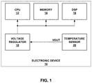
- FIG. 1 is a block diagram illustrating an example electronic device that includes a temperature sensor.
- FIG. 2 is a block diagram illustrating an example temperature sensor in accordance with this disclosure.
- FIG. 3 is a graph illustrating a dependence of parallel and anti-parallel magnetization state conductance of a magnetic tunnel junction (MTJ) device on temperature.
- MTJ magnetic tunnel junction
- FIG. 4 is a block diagram illustrating another example temperature sensor in accordance with this disclosure.
- FIG. 5 is a graph illustrating output voltage of the temperature sensor of FIG. 4 versus temperature.
- FIG. 6 is a graph illustrating output voltage versus temperature at different W/L ratios.
- FIG. 7 is a graph illustrating response time of thermal transient measurement.
- FIG. 8 is a simulation result of overheat cut-off protection.
- FIG. 9A is a structure of an example of an MTJ device configured such that a conductance of the MTJ device is based on sensed temperature for a temperature sensor.
- FIG. 9B is a diagram from a scanning electron microscope (SEM) of an MTJ device for a temperature sensor.
- FIG. 10A is a stand-by state measurement of IC surface temperature.
- FIG. 10B is a temperature profile along the line in FIG. 10A .
- FIG. 10C is a full loading state measurement of IC surface temperature.
- FIG. 10D is a temperature profile along the line in FIG. 10C .
- FIG. 10E is a full loading with MTJ temperature sensor.
- FIG. 10F is a temperature profile along the line in FIG. 10E .
- FIG. 11 is a flowchart illustrating an example method of operation in accordance with this disclosure.
- FIG. 1 is a block diagram illustrating an example electronic device that includes a temperature sensor formed with one or more spintronic components.
- electronic device 10 includes central processing unit (CPU) 12 , memory 14 , digital signal processor (DSP), voltage regulator 18 , and temperature sensor 20 .
- Device 10 may include more or fewer components than those illustrated in FIG. 1 .
- Device 10 may form an integrated circuit (IC) and part of various larger devices like a mobile device, a laptop computer, a desktop, and the like.
- Device 10 of FIG. 1 is an example of a system of chip (SoC) that includes various components for processing.
- SoC system of chip
- Other examples of device 10 may include power driver ICs.
- temperature sensor 20 generates output indicative of the sensed temperature.
- the sensed temperature refers to the temperature at device 10 , as one example.
- the sensed temperature may refer to the temperature surrounding temperature sensor 20 , which may be the ambient temperature is some examples.
- temperature sensor 20 may output a signal indicative of the temperature of device 10 .
- temperature sensor 20 is illustrated as internal to device 10 , in some examples, temperature sensor 20 may be its own separate circuit, chip or device that outputs a signal indicative of sensed temperature.
- voltage regulator 18 receives power from a battery (not shown) and outputs a constant voltage to the components of device 10 .
- the output of temperature sensor 20 may control the operation of voltage regulator 18 .
- temperature sensor 20 outputs a signal V OUT indicative of the sensed temperature, and control the operation of voltage regulator 18 .
- temperature sensor 20 may turn off the operation of voltage regulator 18 , and thereby turn off power to the components of device 10 .
- the voltage level of the voltage that voltage regulator 18 outputs may be based on the output of temperature sensor 20 .
- Device 10 cool downs when voltage regulator 18 stops delivering power or when voltage regulator 18 reduces the voltage delivered to components of device 10 . For example, where voltage regulator 18 scales the output voltage based on the output from temperature sensor 20 , device 10 cools down from the reduced power consumption due of the reduction in the delivered power from voltage regulator 18 .
- CPU 12 , memory 14 , and DSP 16 may be considered as controlled circuits that receive power from voltage regulator 18 .
- the heat generated by the controlled circuits or other components is sensed by temperature sensor 20 , and in response, temperature sensor 20 outputs a signal indicative of the temperature.
- the signal that temperature sensor 20 outputs controls whether voltage regulator 18 delivers power to the controlled circuits.
- the signal that temperature sensor 20 outputs controls the voltage level of the voltage that voltage regulator 18 outputs.
- FIG. 1 illustrates an example where temperature sensor 20 can be adopted in a power source scaling strategy to cool down device 10 in an effective way.
- temperature sensor 20 may be part of CPU 12 , memory 14 , and/or DSP 16 .
- CPU 12 , memory 14 , and/or DSP 16 are formed with spintronic devices (e.g., devices whose state is controlled by spin of currents)
- temperature sensor 20 may be part of CPU 12 , memory 14 , and/or DSP 16 .
- the sensed temperature may be the temperature at CPU 12 , memory 14 , and/or DSP 16 . As described, the sensed temperature may be the temperature of areas proximate to temperature sensor 20 .
- thermoelectric device 10 There may be other purposes for determining the temperature at device 10 . Using the temperature measurement to selectively turn on and off the controlled circuits via voltage regulator 18 is one example.
- temperature sensor 20 is constructed to include one or more spintronic components.
- Spintronic components refer to components where spin of a current (e.g., electrons in a current) can be used to set magnetization states of the spintronic component.
- temperature sensor 20 may include a magnetic tunnel junction (MTJ) device that includes a free layer and a fixed layer sandwiched by an insulator layer. A magnetization direction of the fixed layer cannot be changed, but a magnetization direction of the free layer can be changed.
- the MTJ device which is an example of a spintronic device, is referred to being in a parallel magnetization state.
- the MTJ device is referred to being in an anti-parallel magnetization state.
- STT-MTJ spin-transfer torque operated MTJ
- current flowing through the MTJ sets the magnetization state.
- current flowing through the MTJ in a first direction applies a torque on the free layer, and sets the magnetization direction of the free layer to be the same as the magnetization direction of the fixed layer (e.g., places the STT-MTJ in the parallel magnetization state).
- Current flowing through the MTJ in a second, opposite direction applies an opposite torque on the free layer, and sets the magnetization direction of the free layer to the opposite as the magnetization direction of the fixed layer (e.g., places the STT-MTJ in the anti-parallel magnetization state).
- the techniques are not so limited.
- the techniques may be applicable to MTJs in addition to STT-MTJs.
- the magnetization state may be set by current flowing through a spin channel (e.g., set the magnetization state based on spin wave, spin Hall effect and/or Rashiba effect).
- the magnetization sate may be set by other means such as the voltage controlled magnetic anisotropy (VCMA) and the magnetic electrical (ME) effect.
- VCMA voltage controlled magnetic anisotropy
- ME magnetic electrical
- Other examples of spintronic components include a giant magnetoresistance (GMR) device.
- GMR giant magnetoresistance
- Another example of a spintronic component is a topological insulator-based MTJ device.
- the techniques described in this disclosure may be applicable to MTJs, GMRs, or other types of spintronic components.
- STT-MTJ devices described herein may be suitable components for temperature sensor 20 because the devices can be constructed such that the conductance (i.e., inverse of resistance) of an STT-MTJ device, as one example, varies in response to changes in temperatures.
- the STT-MTJ device can be placed in the anti-parallel state and the conductance of the STT-MTJ device may be used to sense changes in the temperature (e.g., increases over temperature or decreases over temperature). If the STT-MTJ device is placed in the parallel state, the STT-MTJ device may be configured such that the conductance of the STT-MTJ device is constant over temperature.
- the conductance of the spintronic component may be constant over temperature in the anti-parallel magnetization state, and increasing or decreasing over temperature in the parallel magnetization state.
- temperature sensor 20 that uses spintronic components for sensing temperature may provide for faster temperature recognition than some other temperature sensor types, such as electron diffusion in CMOS technology. For instance, because the temperature-dependent tunnel magneto-resistance in the MTJ is related to spin wave excitation, the thermal reaction speed of the MTJ may be much faster than that of electron diffusion.
- some conventional temperature sensors compatible with CMOS technology include parasitic lateral or substrate bipolar transistor, MOS transistor, ring-oscillator, etc.
- the conventional temperature sensors use two diode-connected substrate PNP transistors to generate voltage VBE and delta VBE, and these voltages are combined to produce Proportional To Absolute Temperature (PTAT) and reference voltages.
- the PTAT and reference voltages are converted to a digital temperature reading DOUT using an analog-to-digital converter (ADC).
- ADC analog-to-digital converter
- the operation of the CMOS based temperature sensor is based on electron movement from emitter to collector.
- Temperature sensor 20 may provide, in some examples but not necessarily in all examples, faster thermal transit speed as compared to some examples of temperature sensors developed with CMOS.
- temperature sensor 20 may be beneficial for various reasons. As one example, by immediate detection of change in temperature, temperature sensor 20 may more quickly cause voltage regulator 18 to turn off power to the controlled circuits as compared to a temperature sensor developed using CMOS technology. In general, temperature sensor 20 may provide a more accurate temperature reading for an exact moment, as compared to a temperature sensor developed using CMOS technology, because there is lag in the temperature sensing in CMOS technology as compared to spintronic components of temperature sensor 20 .
- temperature sensor 20 is used to regulate the supply voltage of voltage regulator 18 .
- device 10 may be used in current driving mode, working in high voltage (>40 V) and large current (>100 mA). Its die temperature may always be higher than 120° C. Cooling down such kind of IC is helpful to improve its life time and reliability.
- Temperature sensor 20 may continuously measures the die temperature of device 10 . Then, voltage regulator 18 may adaptively change the supply voltage of device 10 according to the measured die temperature. Scaling the supply voltage reduces both the dynamic and leakage power of the chip. In this way, the die temperature can be in a controllable manner.
- FIG. 2 is a block diagram illustrating an example temperature sensor in accordance with this disclosure.
- temperature sensor 20 includes current source 22 and MTJ device 24 (e.g., STT-MTJ device 24 ).
- Current source 22 is one example of a current source, and other examples of current sources are possible.
- transistor MP 1 is a pMOS transistor that always stays in a saturation state. Current flows from VDD, through MP 1 , MTJ device 24 , and ground when switch S is connected to ground. As illustrated, MTJ device 24 includes free layer 26 , tunneling oxide layer 28 , and fixed layer 30 .
- MTJ device 24 may have been, e.g., during manufacturing or initialization, placed in the anti-parallel state by running current through MTJ device 24 that causes free layer 26 to be magnetized in the opposite direction relative to fixed layer 30 . Once in the anti-parallel state, MTJ device 24 may remain in the anti-parallel state until sufficient current flows through to cause the magnetization direction of free layer 26 to switch. In one or more examples, the amplitude of the current that current source 22 outputs may not be sufficient to cause the magnetization direction of free layer 26 to switch.
- the conductance of MTJ device 24 may be based on whether MTJ device 24 is in the anti-parallel or parallel magnetization state. In the parallel magnetization state, the conductance of MTJ device 24 is at a first level, and in the parallel magnetization stage, the conductance of MTJ device 24 is at a second level. The first level may be greater than the second level. In other words, the resistance of MTJ device 24 in the parallel magnetization state is less than the resistance of MTJ device 24 in the anti-parallel magnetization state.
- the conductance of MTJ device 24 may be based on the sensed temperature (e.g., temperature proximate to MTJ device 24 such as temperature of device 10 ).
- MTJ device 24 may be configured such that a conductance of MTJ device 24 is based on sensed temperature. For instance, if MTJ device 24 is in a first state (e.g., anti-parallel magnetization state), the conductance of MTJ device 24 may change based on the sensed temperature. Therefore, the voltage at node 25 may change based on the sensed temperature. Accordingly, in some examples, the voltage at node 25 may be indicative of the sensed temperature of device 10 .
- temperature sensor 20 may include amplifier 32 to amplify the voltage at node 25 and generate an output voltage (e.g., signal) indicative of the sensed temperature. This output voltage V OUT may control the operation of voltage regulator 18 as described above.
- the voltage at node 25 may be subtracted from a reference voltage generated from reference voltage source (V REF ) 26 .
- amplifier 32 may be configured as a difference amplifier that determines the difference between the voltage at node 25 and the voltage from V REF 26 to generate an output voltage indicative of the sensed temperature.
- V REF 26 and amplifier 32 configured as a difference amplifier may not be necessary in every example.
- One example of a difference amplifier is illustrated in more detail in FIG. 4 .
- FIG. 2 illustrates a schematic of one example of STT-MTJ temperature sensor 20 , including a correction method for inter-die process variation.
- MTJ device 24 is set in the anti-parallel magnetization state during temperature measurement. Since conductance of MTJ device 24 depends on sensed temperature, the voltage at node 25 can reflect the temperature variation directly.
- the voltage level of V REF 26 may be set based on calibration measurements of the inter-die process variation. By using V REF 26 and difference amplifier 32 , the effect of inter-die process variation is significantly minimized by the calibration procedure.
- FIG. 2 illustrates an example of a device that includes a spintronic component (e.g., STT-MTJ device 26 ), and circuitry (e.g., amplifier 32 ) coupled to MTJ device 26 configured to generate an electrical signal (e.g., voltage at node 25 or V OUT ) indicative of sensed temperature at device 10 based on a conductance of the spintronic component.
- MTJ device 26 is in an anti-parallel magnetization state, where in the anti-parallel magnetization state, a magnetization direction of a first layer (e.g., free layer 26 ) and a second layer (e.g., fixed layer 30 ) of MTJ device 24 is different.
- the device 10 may include a current source 22 (e.g., MP 1 , MN 1 ) configured to output a current through MTJ device 24 generating a voltage at node 25 of MTJ device 24 , where the voltage at node 25 is based on the conductance of MTJ device 24 .
- the circuitry e.g., amplifier 32
- temperature sensor 20 may include a V REF 26 to calibrate the voltage at MTJ device 24 .
- the circuitry e.g., amplifier 32 configured as a difference amplifier
- amplifier 32 configured as a difference amplifier
- the circuitry is configured to receive the voltage at node 25 of MTJ device 24 and the reference voltage from V REF 26 and generate the electrical signal indicative of the sensed temperature at the device.
- Tunneling oxide layer 28 may be formed as a MgO layer.
- the conductance of MTJ device 24 may be based on thickness of MgO layer. For instance, an amount of change in the conductance of MTJ device 24 due to a change in the sensed temperature is based on a thickness of the MgO layer).
- FIG. 3 is a graph illustrating a dependence of parallel and anti-parallel magnetization state conductance of an MTJ device on temperature.
- the example MTJ device configured such that its conductance is based on sensed temperature and used to generate this data is illustrated in more detail with respect to FIG. 9A .
- FIG. 3 includes both measured data for the MTJ device, and calculated values.
- FIG. 3 illustrates conductance (G) for both MTJ device 24 in the parallel and anti-parallel magnetization state versus temperature based on actual measurement and theory analysis.
- the conductance in the parallel magnetization state (GP) of MTJ device 24 may be independent of temperature. In other words, the conductance of MTJ device 24 may not change over temperature if MTJ device 26 is configured in the parallel magnetization state.
- the conductance of MTJ device 24 in anti-parallel magnetization state increases monotonically with increasing temperature. Accordingly, the dependence of the conductance of MTJ device 24 , in an anti-parallel magnetization state, on temperature can be used to measure temperature.
- a magnetization direction of a first layer and a second layer of the MTJ device 24 is the same, and in the anti-parallel state, a magnetization direction of a first layer and a second layer of the MTJ device 24 is different.
- this disclosure describes an example of a device that includes a spintronic component (e.g., STT-MTJ device 24 ) used for determining a temperature of the device.
- a spintronic component e.g., STT-MTJ device 24
- the conductance of the spintronic component is based on the temperature of the device.
- FIG. 4 is a block diagram illustrating another example temperature sensor in which multiple spintronic components are incorporated within the sensor in accordance with this disclosure.
- FIG. 4 is a schematic of temperature sensor 20 based on two MTJ devices 24 , 36 .
- the example illustrated in FIG. 4 may compensate for temperature variations in the circuitry needed to generate the current that flows through MTJ device 24 .
- current source 22 generates the current that flows through MTJ device 24 .
- the operations of the MP 1 and MN 1 transistors of current source 22 may depend upon the sensed temperature.
- the threshold voltage at which MP 1 and MN 1 transistors conduct may change over temperature.
- two MTJ devices 24 , 36 to determine two voltages, and then subtracting the voltages, any effect of the transistors due to temperature may be minimized.
- Additional spintronic components may be used than MTJ devices 24 , 36 to minimize effects of the transistors due to temperature.
- MTJ device 36 may be substantially similar to MTJ device 24 ; however, MTJ device 36 may be configured in a parallel magnetization state (e.g., the magnetization direction of the free layer and fixed layer of MTJ device 36 is in the same direction).
- Transistors M 1 , M 2 , and M 4 may generate current I 2
- transistors M 1 , M 2 , and M 3 may generate current I 1 .
- transistor M 4 may mirror the current flowing through transistors M 1 and M 2 as current I 2
- transistor M 3 may mirror the current flowing through transistor M 1 and M 2 as current I 1 .
- Difference circuit 34 may determine the difference between V 2 and V 1 (e.g., determine V 1 ⁇ V 2 ). For example, V OUT from difference circuit 34 is proportional to the (V 1 ⁇ V 2 ).
- Difference circuit 34 includes an operational amplifier, and resistors R 1 , R 2 , and Rf, as illustrated. In examples where amplifier 32 of FIG. 2 is a difference amplifier, difference circuit 34 may replace amplifier 32 in FIG. 2 . Difference circuit 34 is one example way in which to determine the difference between V 1 and V 2 . Other examples of difference circuits are possible.
- MTJ device 24 is in the anti-parallel magnetization stage, and therefore, the conductance of MTJ device 24 is a function of temperature. Also, the operation of transistors M 1 , M 2 , and M 4 may be dependent upon temperature. Therefore, any variation in the voltage level of V 2 over temperature may be due to change in conductance of MTJ device 24 and due to transistors M 1 , M 2 , and M 4 .
- transistors M 3 and M 4 are substantially the same, including identical, then transistors M 3 and M 4 may exhibit the same behavior due to changes in the sensed temperature. Accordingly, by subtracting voltage V 2 from voltage V 1 , the effect on the voltage level of V 1 and V 2 due to transistors M 1 , M 2 , M 3 , and M 4 may be minimized. The result of the subtraction is indicative a voltage signal indicative of the change in the conductance of MTJ device 24 , which changes due to temperature. Therefore, the voltage signal V OUT of difference circuit 34 is indicative of the sensed temperature.
- a differential circuit 34 is used to minimize the temperature dependence on threshold voltage (Vth) of the MOS transistors M 1 , M 2 , M 3 , and M 4 .
- Temperature sensor 20 may show a linear sensitivity over a wide temperature range.
- Two MTJ devices 24 , 36 are used in the design. MTJ device 24 is in anti-parallel magnetization state while MTJ device 36 is in parallel magnetization state.
- the voltage difference between V 1 and V 2 is amplified using the differential amplifier (e.g., difference circuit 34 ). Accordingly, any variations from MTJ technology may be cancelled by the differentiate manipulation.
- FIG. 4 illustrates an example of a device that includes MTJ device 24 (e.g., a first spintronic component) and MTJ device 36 (e.g., a second spintronic component).
- a first current source e.g., I 2
- I 2 is configured to output a first current through the first spintronic component generating a first voltage (V 2 ), where the first voltage is based on the conductance of the first spintronic component.
- a second current source (e.g., I 1 ) is configured to output a second current through the second spintronic component generating a second voltage (V 1 ), where the second voltage at the second STT-MTJ device is based on the conductance of the second STT-MTJ device.
- the circuitry e.g., R 1 , R 2 , Rf, and the op-amp
- FIG. 5 is a graph illustrating an output voltage of the temperature sensor of FIG. 4 versus temperature. Simulation is performed to verify the correct function of the temperature sensor 20 , as shown in FIG. 5 , showing a wide range of linear relationship between the output signal V OUT and the temperature.
- the voltage V 2 is a function of temperature behavior of the transistors and the conductance of MTJ device 24 over temperature.
- the voltage V 1 is a function of temperature behavior of the transistors.
- V OUT is based on V 1 ⁇ V 2 , and as illustrated increases over temperature. This is because the conductance of MTJ device 24 increases over temperature, meaning lower resistance. Because the resistance of MTJ device 24 is decreasing over temperature, the voltage V 2 is decreasing over temperature. Accordingly, V 1 ⁇ V 2 increases over temperature. Because V OUT is proportional to V 1 ⁇ V 2 , V OUT is shown as increasing over temperature in FIG. 5 .
- FIG. 6 is a graph illustrating output voltage versus temperature at different W/L ratios.
- transistors M 1 , M 2 , M 3 , and M 4 of FIG. 4 may be defined by their widths (W) and lengths (L).
- W widths
- L lengths
- temperature sensor 20 can be designed to have sufficient linear sensitivity.
- the changing rate of the output voltage, V OUT , over temperature, T is determined by W/L of transistor in current mirror circuit (e.g., transistors used to make the I 1 and I 2 currents in FIG. 4 ).
- FIG. 6 shows the simulation result of the relationship between V OUT and temperature for a range of 200K-400K with W/L ratios varied from 1 to 20.
- the voltage-temperature ratio is simulated to be ⁇ 2 mV/K.
- FIG. 7 is a graph illustrating response time of thermal transient measurement.
- temperature sensor 20 based on spintronic components such as MTJ device 24 may have a short response time to temperature changes as compared to CMOS based temperature sensors.
- FIG. 7 shows the measured thermal transient response of the MTJ thermal sensor (e.g., temperature sensor 20 ).
- the input is driven with positive voltage (e.g., device 10 is given power causing it to heat) and, as illustrated in FIG. 7 , there is a positive peak in the response of thermal transient measurement.
- the scenario happens for both MTJ sensor (e.g., temperature sensor 20 ) and CMOS BJT sensor.
- FIG. 7 shows the measured thermal transient response of the MTJ thermal sensor (e.g., temperature sensor 20 ).
- the thermal transient time for MTJ sensor is about 0.5 ns, while the time of CMOS sensor is 6 nano-seconds (ns).
- the speed of thermal transient response of the MTJ sensor is ten times faster than that of CMOS sensor.
- This fast-thermal transient property may be for some examples of MTJ thermal sensor.
- One possible reason for this high response speed is that the mechanism of thermal transportation of MTJ device 24 is spin-wave excitation.
- the transient time is less than 1 ns.
- MTJ device 24 may be configured such that a change in conductance of MTJ device 24 occurs in less than 1 ns responsive to a change in the sensed temperature.
- a voltage at MTJ device 24 may be based on the sensed temperature.
- MTJ device 24 may generate the voltage in less than 1 ns responsive to a change in the sensed temperature.
- one way to reduce the switching time is to increase the amplitude of I (i.e., the current through MTJ device 24 , which is current I 2 in FIG. 4 ). Since the amplitude I is in the denominator of the equation and Ic 0 is subtracted from I, increasing I would reduce the value of “t.” Simulation shows that by changing the amplitude of the current I 2 , the switching time may be reduced to 3.31 ns, 2.5 ns, 1.87 ns, or 1.03 ns, and even less than 1 ns, as a few examples.
- Example current amplitudes for 12 include 3.4 mA, 4.8 mA, and 6.6 mA. Accordingly, the thermal switching may be in nano-seconds at suitable pulse amplitude of current I. For instance, the amplitude of current I should not be so large as to reset the magnetization state of MTJ device 24 to parallel magnetization state.
- Table 1 below is a comparison between use of MTJ device 24 and CMOS BJT sensor.
- FIG. 8 is a simulation result of overheat cut-off protection.
- the example temperature sensor 20 may be adopted directly as an overheat protector.
- temperature sensor 20 may control whether voltage regulator 18 delivers power to the other controlled circuits. If device 10 overheats, temperature sensor 20 may cause to voltage regulator 18 to turn off power relatively quickly because of the fast-thermal response time of MTJ device 24 .
- FIG. 8 shows the simulation result of overheat protection using the STT-MTJ device 24 by temperature sweeping, indicating that the protection circuit (e.g., control of voltage regulator 18 ) can be operated without any lag and thermal oscillation.
- the property of fast thermal transient response of MTJ device 24 may reduce the active power consumption of IC circuit (e.g., device 10 ), and hence to control the die temperature in an effective way.
- MTJ device 24 is prepared by using a magnetron sputtering system and patterned with photolithography. MTJ device 24 is then etched using an argon ion milling process and electrodes are deposited using an electron beam evaporation process.
- the complete structure of MTJ device 24 was Ta 2 nm/(Al 10 nm/Cu 3 nm)(5)/Al 5 nm/Ta 3 nm/Ru 3 nm/IrMn 10 nm/CoFe 2.5 nm/Ru 0.8 nm/CoFeB 3 nm/MgO (0.7 nm-2.5 nm)/CoFeB 3 nm/Ru 3 nm/Ta 10 nm/Ru 7 nm and the size of the fabricated devices was 2 ⁇ m ⁇ 6 ⁇ m.
- Resistance value of MTJ device 24 could be adjusted by tuning the thickness of tunneling barrier MgO.
- the sensitivity of MTJ device 24 e.g., change in conductance in response to a change in temperature
- the thickness of the MgO layer can be adjusted by tuning the thickness of the MgO layer. As one example, if the MgO layer is made thinner, the resistance of MTJ device 24 is decreased (e.g., conductance is increased), and if the MgO layer is made thicker, the resistance of MTJ device 24 is increased (e.g., conductance is decreased). Therefore, an amount of change in the conductance of MTJ device 24 due to a change in the sensed temperature is based on a thickness of the MgO layer.
- the sensitivity of temperature sensor 20 may be based on the thickness of the MgO layer.
- the sensitivity of temperature sensor 20 may be a measure of how small of changes in the temperature can be sensed by temperature sensor 20 . If small changes in the sensed temperature result in greater change in the conductance of MTJ device 24 , as compared to less change in the conductance of MTJ device 24 , then the sensitivity of temperature sensor 20 may be considered as being more sensitive to temperature changes. As an example, if the change in temperature is X, then the change in conductance of MTJ device 24 may be Y for a first thickness of the MgO layer, and the conductance of MTJ device 24 may be Z for a second thickness of the MgO layer.
- Y may be greater than Z, and the first thickness may be less than the second thickness.
- MTJ device 24 may be configured for different sensitivities of temperature sensor 20 .
- the thickness of the MgO layer may control the slope of the conductance versus temperature line for MTJ device 24 being in the anti-parallel state as illustrated in FIG. 3 .
- FIG. 9A is a structure of MTJ device 24 for temperature sensor 20 configured such that a conductance of MTJ device 24 is based on sensed temperature
- FIG. 9B is a diagram from a scanning electron microscope (SEM) of MTJ device 24 for temperature sensor 24 .
- SEM scanning electron microscope
- FIGS. 9A and 9B The magnetic properties are measured in a physical properties measurement system (PPMS) using a standard four-probe technique with a sensing current of 0.05 mA.
- PPMS physical properties measurement system
- MTJ device 24 used for temperature sensor 20 is merely one example, and the techniques described in this disclosure should not be considered limited to those examples.
- other structures of MTJ devices may be used as many MTJ devices exhibit thermal dependency.
- STT-MTJ devices are one type of spintronic components, and others may be used as well including spintronic components not necessarily limited having spin torque transfer (STT) properties.
- STT-GMR devices may be possible, including STT-GMR devices.
- the following provides the results on the package temperature with the MTJ thermal sensor (e.g., temperature sensor 20 ) as the input of supply voltage regulator 18 .
- the driver IC For the driver IC with stand-by mode, its temperature profile is shown in FIG. 10A and FIG. 10B , showing maximum temperature 30.76° C.
- the driver e.g., example where device 10 is a power driver IC
- FIG. 10C and FIG. 10D its surface temperature increased dramatically.
- the maximum temperature reached is 121.02° C., which may have negative impacts on the IC.
- FIG. 10E and FIG. 10F by utilizing temperature sensor 20 having spintronic component (e.g., MTJ device 24 ) as input of supply voltage regulator 18 , the temperature is decreased.
- the maximum temperature with regulation from temperature sensor 20 is 71.83° C.
- FIG. 11 is a flowchart illustrating an example method of operating in accordance with this disclosure. For ease of illustration, the example of FIG. 11 is described with respect to FIGS. 2 and 4 .
- a current source may output a current through a spintronic component that generates a voltage at the spintronic component ( 36 ).
- the voltage at the spintronic component is based on a sensed temperature.
- the spintronic component is configured such that a conductance of the spintronic component is based on the sensed temperature.
- the spintronic component include MTJ device 24 , which may be an example of a STT-MTJ device.
- current source 22 may output a current through MTJ device 24 to generate a voltage at node 25 , where the voltage at node 25 is based on the conductance of MTJ device 24 .
- transistor M 4 may mirror the current flowing through transistors M 1 and M 2 to output a current I 2 through MTJ device 24 to generate a voltage V 2 .
- Circuitry may generate an electrical signal indicative of the sensed temperature (e.g., temperature proximate to the spintronic component such as that of device 10 ) based on the voltage at the spintronic component ( 38 ).
- amplifier 32 may output V OUT , which is an electrical signal indicative of the sensed temperature based on the voltage at node 25 .
- transistor M 3 may mirror the current flowing through transistors M 1 and M 2 to output a current I 1 through MTJ device 36 to generate a voltage V 1 .
- MTJ device 36 may be configured in a parallel magnetization state.
- Difference circuit 34 may subtract V 2 from V 1 (e.g., determine V 1 ⁇ V 2 ). The result may be the electrical signal indicative of the sensed temperature.
- Voltage regulator 18 may control operation of an electronic device 10 based on the generated electrical signal ( 40 ). For example, voltage regulator 18 may control the voltage applied to one or more controlled circuits of electronic device 10 based on the generated electrical signal. As one example, voltage regulator 18 may scale a supply voltage based on the generated electrical signal from temperature sensor 20 to limit the power delivered to the controlled circuits, thereby cooling the controlled circuits. As another example, voltage regulator 18 may stop delivery of supply voltage based on the generated electrical signal from temperature sensor 20 to stop the operation of electronic device 10 .
Abstract
Description
t=ln(pi/(2*alpha))/(abs(I−Ic0),
where alpha is an initial angle between magnetizations and set by thermal fluctuations or magnetic pinning, Ic0 is critical current at temperature=0, and I is the current through
| TABLE 1 |
| Comparison between MTJ sensor and CMOS BJT sensor |
| Temperature Range | Inaccuracy | Thermal transit time | ||
| MTJ sensor | −100~200° C. | 0.5~0.6° C. | 0.5 | ns |
| CMOS BJT | −50~120° C. | 0.3~0.5° C. | 5~6 | ns |
| sensor | ||||
Claims (26)
Priority Applications (1)
| Application Number | Priority Date | Filing Date | Title |
|---|---|---|---|
| US15/828,976 US10794774B2 (en) | 2016-12-02 | 2017-12-01 | Spintronic temperature sensor |
Applications Claiming Priority (2)
| Application Number | Priority Date | Filing Date | Title |
|---|---|---|---|
| US201662429301P | 2016-12-02 | 2016-12-02 | |
| US15/828,976 US10794774B2 (en) | 2016-12-02 | 2017-12-01 | Spintronic temperature sensor |
Publications (2)
| Publication Number | Publication Date |
|---|---|
| US20180156672A1 US20180156672A1 (en) | 2018-06-07 |
| US10794774B2 true US10794774B2 (en) | 2020-10-06 |
Family
ID=62243008
Family Applications (1)
| Application Number | Title | Priority Date | Filing Date |
|---|---|---|---|
| US15/828,976 Active 2038-09-18 US10794774B2 (en) | 2016-12-02 | 2017-12-01 | Spintronic temperature sensor |
Country Status (1)
| Country | Link |
|---|---|
| US (1) | US10794774B2 (en) |
Families Citing this family (3)
| Publication number | Priority date | Publication date | Assignee | Title |
|---|---|---|---|---|
| JP6791180B2 (en) * | 2018-03-01 | 2020-11-25 | Tdk株式会社 | Sensor |
| CN110260999B (en) * | 2019-06-14 | 2020-10-16 | 北京航空航天大学 | Temperature sensor, assembly and temperature measuring method |
| KR20230008761A (en) * | 2020-04-29 | 2023-01-16 | 유니버시티 오브 써던 캘리포니아 | Magnetoelectric sensor for hardware trojan detection |
Citations (3)
| Publication number | Priority date | Publication date | Assignee | Title |
|---|---|---|---|---|
| US20070077664A1 (en) * | 2005-09-30 | 2007-04-05 | Chung Young S | Magnetic tunnel junction temperature sensors and methods |
| US20170229163A1 (en) * | 2016-02-05 | 2017-08-10 | Tdk Corporation | Magnetic Memory |
| US20190074432A1 (en) * | 2017-08-31 | 2019-03-07 | The Regents Of The University Of California | Si-BASED SPINTRONICS DEVICES |
-
2017
- 2017-12-01 US US15/828,976 patent/US10794774B2/en active Active
Patent Citations (3)
| Publication number | Priority date | Publication date | Assignee | Title |
|---|---|---|---|---|
| US20070077664A1 (en) * | 2005-09-30 | 2007-04-05 | Chung Young S | Magnetic tunnel junction temperature sensors and methods |
| US20170229163A1 (en) * | 2016-02-05 | 2017-08-10 | Tdk Corporation | Magnetic Memory |
| US20190074432A1 (en) * | 2017-08-31 | 2019-03-07 | The Regents Of The University Of California | Si-BASED SPINTRONICS DEVICES |
Non-Patent Citations (9)
Also Published As
| Publication number | Publication date |
|---|---|
| US20180156672A1 (en) | 2018-06-07 |
Similar Documents
| Publication | Publication Date | Title |
|---|---|---|
| US10794774B2 (en) | Spintronic temperature sensor | |
| US8063634B2 (en) | Electronic circuit and method for resetting a magnetoresistance element | |
| US7268523B2 (en) | Constant voltage power supply circuit and method of testing the same | |
| US8177426B2 (en) | Sub-threshold CMOS temperature detector | |
| EP2480947B1 (en) | Compensated bandgap | |
| US7973527B2 (en) | Electronic circuit configured to reset a magnetoresistance element | |
| US10585152B2 (en) | Temperature-compensated magneto-resistive sensor | |
| US20140327437A1 (en) | Current sensor | |
| US9958512B2 (en) | Low-power magnetic resistance switch sensor | |
| JP4031447B2 (en) | Offset adjustable differential amplifier | |
| US10571296B2 (en) | Circuit, method and sensor for obtaining information on a physical quantity | |
| US11525875B2 (en) | Reducing voltage non-linearity in a bridge having tunneling magnetoresistance (TMR) elements | |
| US7825656B2 (en) | Temperature compensation for spaced apart sensors | |
| US7703975B2 (en) | Temperature detecting circuit | |
| Borole et al. | Design, fabrication, and characterization of giant magnetoresistance (GMR) based open-loop current sensor with U-shaped current carrying conductor | |
| JP5857687B2 (en) | Current detection device, current detection element, and current detection method | |
| US9778067B2 (en) | Sensing a physical quantity in relation to a sensor | |
| Jiang et al. | Fast spintronic thermal sensor for IC power driver cooling down | |
| KR20120072550A (en) | Sensing amplifier circuit of memory | |
| Qoutb et al. | Spintronic/CMOS-based thermal sensors | |
| Qoutb et al. | PMTJ temperature sensor utilizing VCMA | |
| JP6116694B2 (en) | Magnetic field detector with magnetoresistive effect element and current detector | |
| Weitensfelder et al. | Comparison of Sensitivity and Low Frequency Noise Contributions in GMR and TMR Spin Valve Sensors with a Vortex State Free Layer | |
| Qoutb et al. | Distributed spintronic/CMOS sensor network for thermal-aware systems | |
| CN115542206A (en) | Integrated sensor |
Legal Events
| Date | Code | Title | Description |
|---|---|---|---|
| FEPP | Fee payment procedure |
Free format text: ENTITY STATUS SET TO UNDISCOUNTED (ORIGINAL EVENT CODE: BIG.); ENTITY STATUS OF PATENT OWNER: SMALL ENTITY |
|
| FEPP | Fee payment procedure |
Free format text: ENTITY STATUS SET TO SMALL (ORIGINAL EVENT CODE: SMAL); ENTITY STATUS OF PATENT OWNER: SMALL ENTITY |
|
| STPP | Information on status: patent application and granting procedure in general |
Free format text: DOCKETED NEW CASE - READY FOR EXAMINATION |
|
| AS | Assignment |
Owner name: NATIONAL SCIENCE FOUNDATION, VIRGINIA Free format text: CONFIRMATORY LICENSE;ASSIGNOR:UNIVERSITY OF MINNESOTA;REEL/FRAME:045974/0214 Effective date: 20180418 |
|
| AS | Assignment |
Owner name: REGENTS OF THE UNIVERSITY OF MINNESOTA, MINNESOTA Free format text: ASSIGNMENT OF ASSIGNORS INTEREST;ASSIGNOR:WANG, JIAN-PING;REEL/FRAME:048456/0700 Effective date: 20181228 Owner name: REGENTS OF THE UNIVERSITY OF MINNESOTA, MINNESOTA Free format text: ASSIGNMENT OF ASSIGNORS INTEREST;ASSIGNOR:JIANG, YANFENG;REEL/FRAME:048456/0835 Effective date: 20190105 |
|
| STPP | Information on status: patent application and granting procedure in general |
Free format text: NON FINAL ACTION MAILED |
|
| STPP | Information on status: patent application and granting procedure in general |
Free format text: RESPONSE TO NON-FINAL OFFICE ACTION ENTERED AND FORWARDED TO EXAMINER |
|
| STPP | Information on status: patent application and granting procedure in general |
Free format text: NON FINAL ACTION MAILED |
|
| STPP | Information on status: patent application and granting procedure in general |
Free format text: NOTICE OF ALLOWANCE MAILED -- APPLICATION RECEIVED IN OFFICE OF PUBLICATIONS |
|
| STPP | Information on status: patent application and granting procedure in general |
Free format text: PUBLICATIONS -- ISSUE FEE PAYMENT VERIFIED |
|
| STCF | Information on status: patent grant |
Free format text: PATENTED CASE |
|
| MAFP | Maintenance fee payment |
Free format text: PAYMENT OF MAINTENANCE FEE, 4TH YR, SMALL ENTITY (ORIGINAL EVENT CODE: M2551); ENTITY STATUS OF PATENT OWNER: SMALL ENTITY Year of fee payment: 4 |