US10787537B2 - Synthesis of polymers for organic photovoltaics - Google Patents
Synthesis of polymers for organic photovoltaics Download PDFInfo
- Publication number
- US10787537B2 US10787537B2 US16/253,992 US201916253992A US10787537B2 US 10787537 B2 US10787537 B2 US 10787537B2 US 201916253992 A US201916253992 A US 201916253992A US 10787537 B2 US10787537 B2 US 10787537B2
- Authority
- US
- United States
- Prior art keywords
- polymer
- difluoro
- bithiophene
- coupling
- produce
- Prior art date
- Legal status (The legal status is an assumption and is not a legal conclusion. Google has not performed a legal analysis and makes no representation as to the accuracy of the status listed.)
- Active, expires
Links
- 229920000642 polymer Polymers 0.000 title description 67
- 238000013086 organic photovoltaic Methods 0.000 title description 17
- 230000015572 biosynthetic process Effects 0.000 title description 7
- 238000003786 synthesis reaction Methods 0.000 title description 4
- 238000000034 method Methods 0.000 claims abstract description 23
- 230000008878 coupling Effects 0.000 claims abstract description 16
- 238000010168 coupling process Methods 0.000 claims abstract description 16
- 238000005859 coupling reaction Methods 0.000 claims abstract description 16
- 229910052794 bromium Inorganic materials 0.000 claims abstract description 6
- 150000001875 compounds Chemical class 0.000 claims abstract description 6
- 150000002148 esters Chemical class 0.000 claims abstract description 6
- 125000003638 stannyl group Chemical group [H][Sn]([H])([H])* 0.000 claims abstract description 5
- -1 3,3′-difluoro-[2,2′-bithiophene]-5,5′-diyl Chemical group 0.000 claims description 11
- UKHQRARQNZOXRL-UHFFFAOYSA-N trimethyltin Chemical compound C[SnH](C)C UKHQRARQNZOXRL-UHFFFAOYSA-N 0.000 claims description 8
- 238000006116 polymerization reaction Methods 0.000 claims description 5
- PCLIMKBDDGJMGD-UHFFFAOYSA-N N-bromosuccinimide Chemical compound BrN1C(=O)CCC1=O PCLIMKBDDGJMGD-UHFFFAOYSA-N 0.000 claims description 4
- 238000005700 Stille cross coupling reaction Methods 0.000 claims description 4
- 238000006069 Suzuki reaction reaction Methods 0.000 claims description 3
- 238000006254 arylation reaction Methods 0.000 claims description 3
- 230000000379 polymerizing effect Effects 0.000 claims description 3
- NCWDBNBNYVVARF-UHFFFAOYSA-N 1,3,2-dioxaborolane Chemical compound B1OCCO1 NCWDBNBNYVVARF-UHFFFAOYSA-N 0.000 claims description 2
- UCFSYHMCKWNKAH-UHFFFAOYSA-N 4,4,5,5-tetramethyl-1,3,2-dioxaborolane Chemical group CC1(C)OBOC1(C)C UCFSYHMCKWNKAH-UHFFFAOYSA-N 0.000 claims description 2
- ZADPBFCGQRWHPN-UHFFFAOYSA-N boronic acid Chemical compound OBO ZADPBFCGQRWHPN-UHFFFAOYSA-N 0.000 claims description 2
- 230000031709 bromination Effects 0.000 claims description 2
- 238000005893 bromination reaction Methods 0.000 claims description 2
- PIILXFBHQILWPS-UHFFFAOYSA-N tributyltin Chemical compound CCCC[Sn](CCCC)CCCC PIILXFBHQILWPS-UHFFFAOYSA-N 0.000 claims description 2
- 239000000243 solution Substances 0.000 description 57
- MVPPADPHJFYWMZ-UHFFFAOYSA-N chlorobenzene Chemical compound ClC1=CC=CC=C1 MVPPADPHJFYWMZ-UHFFFAOYSA-N 0.000 description 45
- 239000010410 layer Substances 0.000 description 40
- CSCPPACGZOOCGX-UHFFFAOYSA-N Acetone Chemical compound CC(C)=O CSCPPACGZOOCGX-UHFFFAOYSA-N 0.000 description 39
- 239000010408 film Substances 0.000 description 27
- 239000000758 substrate Substances 0.000 description 25
- HEDRZPFGACZZDS-UHFFFAOYSA-N Chloroform Chemical compound ClC(Cl)Cl HEDRZPFGACZZDS-UHFFFAOYSA-N 0.000 description 24
- VLKZOEOYAKHREP-UHFFFAOYSA-N n-Hexane Chemical class CCCCCC VLKZOEOYAKHREP-UHFFFAOYSA-N 0.000 description 21
- XKRFYHLGVUSROY-UHFFFAOYSA-N Argon Chemical compound [Ar] XKRFYHLGVUSROY-UHFFFAOYSA-N 0.000 description 18
- OKKJLVBELUTLKV-UHFFFAOYSA-N Methanol Chemical compound OC OKKJLVBELUTLKV-UHFFFAOYSA-N 0.000 description 15
- CYPYTURSJDMMMP-WVCUSYJESA-N (1e,4e)-1,5-diphenylpenta-1,4-dien-3-one;palladium Chemical compound [Pd].[Pd].C=1C=CC=CC=1\C=C\C(=O)\C=C\C1=CC=CC=C1.C=1C=CC=CC=1\C=C\C(=O)\C=C\C1=CC=CC=C1.C=1C=CC=CC=1\C=C\C(=O)\C=C\C1=CC=CC=C1 CYPYTURSJDMMMP-WVCUSYJESA-N 0.000 description 13
- 239000007787 solid Substances 0.000 description 13
- PBKONEOXTCPAFI-UHFFFAOYSA-N 1,2,4-trichlorobenzene Chemical compound ClC1=CC=C(Cl)C(Cl)=C1 PBKONEOXTCPAFI-UHFFFAOYSA-N 0.000 description 12
- MCEWYIDBDVPMES-UHFFFAOYSA-N [60]pcbm Chemical compound C123C(C4=C5C6=C7C8=C9C%10=C%11C%12=C%13C%14=C%15C%16=C%17C%18=C(C=%19C=%20C%18=C%18C%16=C%13C%13=C%11C9=C9C7=C(C=%20C9=C%13%18)C(C7=%19)=C96)C6=C%11C%17=C%15C%13=C%15C%14=C%12C%12=C%10C%10=C85)=C9C7=C6C2=C%11C%13=C2C%15=C%12C%10=C4C23C1(CCCC(=O)OC)C1=CC=CC=C1 MCEWYIDBDVPMES-UHFFFAOYSA-N 0.000 description 12
- 125000000217 alkyl group Chemical group 0.000 description 10
- 125000003118 aryl group Chemical group 0.000 description 10
- 125000004432 carbon atom Chemical group C* 0.000 description 10
- 229910052786 argon Inorganic materials 0.000 description 9
- 238000001914 filtration Methods 0.000 description 9
- 239000011701 zinc Substances 0.000 description 9
- HZAXFHJVJLSVMW-UHFFFAOYSA-N 2-Aminoethan-1-ol Chemical compound NCCO HZAXFHJVJLSVMW-UHFFFAOYSA-N 0.000 description 8
- XMWRBQBLMFGWIX-UHFFFAOYSA-N C60 fullerene Chemical compound C12=C3C(C4=C56)=C7C8=C5C5=C9C%10=C6C6=C4C1=C1C4=C6C6=C%10C%10=C9C9=C%11C5=C8C5=C8C7=C3C3=C7C2=C1C1=C2C4=C6C4=C%10C6=C9C9=C%11C5=C5C8=C3C3=C7C1=C1C2=C4C6=C2C9=C5C3=C12 XMWRBQBLMFGWIX-UHFFFAOYSA-N 0.000 description 8
- KFZMGEQAYNKOFK-UHFFFAOYSA-N Isopropanol Chemical compound CC(C)O KFZMGEQAYNKOFK-UHFFFAOYSA-N 0.000 description 8
- 239000011248 coating agent Substances 0.000 description 8
- 238000000576 coating method Methods 0.000 description 8
- 229940126214 compound 3 Drugs 0.000 description 8
- 229910003472 fullerene Inorganic materials 0.000 description 8
- JKQOBWVOAYFWKG-UHFFFAOYSA-N molybdenum trioxide Chemical compound O=[Mo](=O)=O JKQOBWVOAYFWKG-UHFFFAOYSA-N 0.000 description 8
- 239000002904 solvent Substances 0.000 description 8
- 238000001704 evaporation Methods 0.000 description 7
- 239000011521 glass Substances 0.000 description 7
- COIOYMYWGDAQPM-UHFFFAOYSA-N tris(2-methylphenyl)phosphane Chemical compound CC1=CC=CC=C1P(C=1C(=CC=CC=1)C)C1=CC=CC=C1C COIOYMYWGDAQPM-UHFFFAOYSA-N 0.000 description 7
- IJGRMHOSHXDMSA-UHFFFAOYSA-N Atomic nitrogen Chemical compound N#N IJGRMHOSHXDMSA-UHFFFAOYSA-N 0.000 description 6
- OKTJSMMVPCPJKN-UHFFFAOYSA-N Carbon Chemical compound [C] OKTJSMMVPCPJKN-UHFFFAOYSA-N 0.000 description 6
- YMWUJEATGCHHMB-UHFFFAOYSA-N Dichloromethane Chemical compound ClCCl YMWUJEATGCHHMB-UHFFFAOYSA-N 0.000 description 6
- 238000000944 Soxhlet extraction Methods 0.000 description 6
- 239000000370 acceptor Substances 0.000 description 6
- 238000006243 chemical reaction Methods 0.000 description 6
- 238000000151 deposition Methods 0.000 description 6
- 230000008021 deposition Effects 0.000 description 6
- 239000000499 gel Substances 0.000 description 6
- AMGQUBHHOARCQH-UHFFFAOYSA-N indium;oxotin Chemical compound [In].[Sn]=O AMGQUBHHOARCQH-UHFFFAOYSA-N 0.000 description 6
- 239000000178 monomer Substances 0.000 description 6
- 230000001376 precipitating effect Effects 0.000 description 6
- 238000010992 reflux Methods 0.000 description 6
- XNWFRZJHXBZDAG-UHFFFAOYSA-N 2-METHOXYETHANOL Chemical compound COCCO XNWFRZJHXBZDAG-UHFFFAOYSA-N 0.000 description 5
- 229910017107 AlOx Inorganic materials 0.000 description 5
- YXCYGIMIRRMIPW-UHFFFAOYSA-N CCCCCCCCCCC(CCCCCCCC)CC1=C(C)SC(C2=C(F)C(F)=C(C3=CC(CC(CCCCCCCC)CCCCCCCCCC)=C(C4=CC(F)=C(C5=C(F)C=C(C6=C(CC(CCCCCCCC)CCCCCCCCCC)C=C(C7=C(F)C(F)=C(C8=CC(CC(CCCCCCCC)CCCCCCCCCC)=C(C9=CC%10=C(C%11=CC=C(CC(CC)CCCC)S%11)C%11=C(C=C(C)S%11)C(C%11=CC=C(CC(CC)CCCC)S%11)=C%10S9)S8)C8=NSN=C87)S6)S5)S4)S3)C3=NSN=C32)=C1 Chemical compound CCCCCCCCCCC(CCCCCCCC)CC1=C(C)SC(C2=C(F)C(F)=C(C3=CC(CC(CCCCCCCC)CCCCCCCCCC)=C(C4=CC(F)=C(C5=C(F)C=C(C6=C(CC(CCCCCCCC)CCCCCCCCCC)C=C(C7=C(F)C(F)=C(C8=CC(CC(CCCCCCCC)CCCCCCCCCC)=C(C9=CC%10=C(C%11=CC=C(CC(CC)CCCC)S%11)C%11=C(C=C(C)S%11)C(C%11=CC=C(CC(CC)CCCC)S%11)=C%10S9)S8)C8=NSN=C87)S6)S5)S4)S3)C3=NSN=C32)=C1 YXCYGIMIRRMIPW-UHFFFAOYSA-N 0.000 description 5
- CSCOPUWQZDXWHJ-UHFFFAOYSA-N CCCCCCCCCCC(CCCCCCCC)CC1=CSC(C2=C(F)C(F)=C(C3=CC(CC(CCCCCCCC)CCCCCCCCCC)=C(C)S3)C3=NSN=C32)=C1 Chemical compound CCCCCCCCCCC(CCCCCCCC)CC1=CSC(C2=C(F)C(F)=C(C3=CC(CC(CCCCCCCC)CCCCCCCCCC)=C(C)S3)C3=NSN=C32)=C1 CSCOPUWQZDXWHJ-UHFFFAOYSA-N 0.000 description 5
- 229940125782 compound 2 Drugs 0.000 description 5
- 239000000284 extract Substances 0.000 description 5
- 239000000203 mixture Substances 0.000 description 5
- 229910052757 nitrogen Inorganic materials 0.000 description 5
- 238000004528 spin coating Methods 0.000 description 5
- 238000004293 19F NMR spectroscopy Methods 0.000 description 4
- IENUTCXHZLZROX-UHFFFAOYSA-N CCCCCCCCCCC(CCCCCCCC)CC1=CSC(C2=C(F)C(F)=C(C3=CC(CC(CCCCCCCC)CCCCCCCCCC)=C(C4=CC(F)=C(C5=C(F)C=C(C6=C(CC(CCCCCCCC)CCCCCCCCCC)C=C(C7=C(F)C(F)=C(C8=CC(CC(C)CCCCCCCC)=CS8)C8=NSN=C87)S6)S5)S4)S3)C3=NSN=C32)=C1 Chemical compound CCCCCCCCCCC(CCCCCCCC)CC1=CSC(C2=C(F)C(F)=C(C3=CC(CC(CCCCCCCC)CCCCCCCCCC)=C(C4=CC(F)=C(C5=C(F)C=C(C6=C(CC(CCCCCCCC)CCCCCCCCCC)C=C(C7=C(F)C(F)=C(C8=CC(CC(C)CCCCCCCC)=CS8)C8=NSN=C87)S6)S5)S4)S3)C3=NSN=C32)=C1 IENUTCXHZLZROX-UHFFFAOYSA-N 0.000 description 4
- NYGVZFFWQRDMTG-UHFFFAOYSA-N CCCCCCCCCCC(CCCCCCCC)CC1=CSC(C2=C(F)C(F)=C(C3=CC(CC(CCCCCCCC)CCCCCCCCCC)=C(C4=CC(F)=C(C5=C(F)C=C(C6=C(CC(CCCCCCCC)CCCCCCCCCC)C=C(C7=C(F)C(F)=C(C8=CC(CC(CCCCCCCC)CCCCCCCCCC)=CS8)C8=NSN=C87)S6)S5)S4)S3)C3=NSN=C32)=C1 Chemical compound CCCCCCCCCCC(CCCCCCCC)CC1=CSC(C2=C(F)C(F)=C(C3=CC(CC(CCCCCCCC)CCCCCCCCCC)=C(C4=CC(F)=C(C5=C(F)C=C(C6=C(CC(CCCCCCCC)CCCCCCCCCC)C=C(C7=C(F)C(F)=C(C8=CC(CC(CCCCCCCC)CCCCCCCCCC)=CS8)C8=NSN=C87)S6)S5)S4)S3)C3=NSN=C32)=C1 NYGVZFFWQRDMTG-UHFFFAOYSA-N 0.000 description 4
- RYGMFSIKBFXOCR-UHFFFAOYSA-N Copper Chemical compound [Cu] RYGMFSIKBFXOCR-UHFFFAOYSA-N 0.000 description 4
- XEEYBQQBJWHFJM-UHFFFAOYSA-N Iron Chemical compound [Fe] XEEYBQQBJWHFJM-UHFFFAOYSA-N 0.000 description 4
- PXHVJJICTQNCMI-UHFFFAOYSA-N Nickel Chemical compound [Ni] PXHVJJICTQNCMI-UHFFFAOYSA-N 0.000 description 4
- LHSHSFDCEZYLMZ-UHFFFAOYSA-N [4-fluoro-5-(3-fluoro-5-trimethylstannylthiophen-2-yl)thiophen-2-yl]-trimethylstannane Chemical compound C[Sn](C1=CC(=C(S1)C=1SC(=CC=1F)[Sn](C)(C)C)F)(C)C LHSHSFDCEZYLMZ-UHFFFAOYSA-N 0.000 description 4
- 238000002835 absorbance Methods 0.000 description 4
- 238000010521 absorption reaction Methods 0.000 description 4
- 229910052782 aluminium Inorganic materials 0.000 description 4
- XAGFODPZIPBFFR-UHFFFAOYSA-N aluminium Chemical compound [Al] XAGFODPZIPBFFR-UHFFFAOYSA-N 0.000 description 4
- 229910052799 carbon Inorganic materials 0.000 description 4
- 229940125904 compound 1 Drugs 0.000 description 4
- 239000010949 copper Substances 0.000 description 4
- 229910052802 copper Inorganic materials 0.000 description 4
- PNOXNTGLSKTMQO-UHFFFAOYSA-L diacetyloxytin Chemical compound CC(=O)O[Sn]OC(C)=O PNOXNTGLSKTMQO-UHFFFAOYSA-L 0.000 description 4
- 230000005525 hole transport Effects 0.000 description 4
- 239000011777 magnesium Substances 0.000 description 4
- 238000005259 measurement Methods 0.000 description 4
- 239000010409 thin film Substances 0.000 description 4
- RFFLAFLAYFXFSW-UHFFFAOYSA-N 1,2-dichlorobenzene Chemical compound ClC1=CC=CC=C1Cl RFFLAFLAYFXFSW-UHFFFAOYSA-N 0.000 description 3
- OCJBOOLMMGQPQU-UHFFFAOYSA-N 1,4-dichlorobenzene Chemical compound ClC1=CC=C(Cl)C=C1 OCJBOOLMMGQPQU-UHFFFAOYSA-N 0.000 description 3
- KZDTZHQLABJVLE-UHFFFAOYSA-N 1,8-diiodooctane Chemical compound ICCCCCCCCI KZDTZHQLABJVLE-UHFFFAOYSA-N 0.000 description 3
- VXKKDOMLXMQOMX-UHFFFAOYSA-N C(CCCCC)C(CC=1C=C(SC=1C=1SC(=CC=1)[Sn](C)(C)C)[Sn](C)(C)C)CCCCCCCC Chemical compound C(CCCCC)C(CC=1C=C(SC=1C=1SC(=CC=1)[Sn](C)(C)C)[Sn](C)(C)C)CCCCCCCC VXKKDOMLXMQOMX-UHFFFAOYSA-N 0.000 description 3
- 0 CC(*)Cc1c(-c2ccc(C(C)(C)C(C)(C)c3c(C)c(N)c(C4=NC(c5cc(*)c(C6NC(C(C)(C)C)=CC6*)[n]5)=C(C[C@](C=I*)NC)*4)c4c(C)[n]pc34)[n]2)[o]c(C(C(C(C(c2cc(CC(*)NIC)c(C(C)(C)C(C)(C)C(*3)=CC(*)=C3c3c(C)cc(-c4c(*=C)c(C)c(-c5c*(C(C(*)*(C)*)C6(C)*)c6[n]5)c5*[n]**45)[n]3)[n]2)=C2C)=*)=*O)=C2N)c1 Chemical compound CC(*)Cc1c(-c2ccc(C(C)(C)C(C)(C)c3c(C)c(N)c(C4=NC(c5cc(*)c(C6NC(C(C)(C)C)=CC6*)[n]5)=C(C[C@](C=I*)NC)*4)c4c(C)[n]pc34)[n]2)[o]c(C(C(C(C(c2cc(CC(*)NIC)c(C(C)(C)C(C)(C)C(*3)=CC(*)=C3c3c(C)cc(-c4c(*=C)c(C)c(-c5c*(C(C(*)*(C)*)C6(C)*)c6[n]5)c5*[n]**45)[n]3)[n]2)=C2C)=*)=*O)=C2N)c1 0.000 description 3
- RPFWFJKQIHOGMU-UHFFFAOYSA-N CCCCCCCCCCC(CCCCCCCC)CC1=C(C)SC(C2=C(F)C(F)=C(C3=CC(CC(CCCCCCCC)CCCCCCCCCC)=C(C4=CC(F)=C(C5=C(F)C=C(C6=C(CC(CCCCCCCC)CCCCCCCCCC)C=C(C7=C(F)C(F)=C(C8=CC(CC(CCCCCCCC)CCCCCCCCCC)=C(Br)S8)C8=NSN=C87)S6)S5)S4)S3)C3=NSN=C32)=C1 Chemical compound CCCCCCCCCCC(CCCCCCCC)CC1=C(C)SC(C2=C(F)C(F)=C(C3=CC(CC(CCCCCCCC)CCCCCCCCCC)=C(C4=CC(F)=C(C5=C(F)C=C(C6=C(CC(CCCCCCCC)CCCCCCCCCC)C=C(C7=C(F)C(F)=C(C8=CC(CC(CCCCCCCC)CCCCCCCCCC)=C(Br)S8)C8=NSN=C87)S6)S5)S4)S3)C3=NSN=C32)=C1 RPFWFJKQIHOGMU-UHFFFAOYSA-N 0.000 description 3
- 229910015711 MoOx Inorganic materials 0.000 description 3
- XUIMIQQOPSSXEZ-UHFFFAOYSA-N Silicon Chemical compound [Si] XUIMIQQOPSSXEZ-UHFFFAOYSA-N 0.000 description 3
- HCHKCACWOHOZIP-UHFFFAOYSA-N Zinc Chemical compound [Zn] HCHKCACWOHOZIP-UHFFFAOYSA-N 0.000 description 3
- 229910007667 ZnOx Inorganic materials 0.000 description 3
- OCFFMJYHZKHRKM-UHFFFAOYSA-N [4,8-bis[5-(2-ethylhexyl)thiophen-2-yl]-2-trimethylstannylthieno[2,3-f][1]benzothiol-6-yl]-trimethylstannane Chemical compound S1C(CC(CC)CCCC)=CC=C1C(C=1SC(=CC=11)[Sn](C)(C)C)=C(C=C(S2)[Sn](C)(C)C)C2=C1C1=CC=C(CC(CC)CCCC)S1 OCFFMJYHZKHRKM-UHFFFAOYSA-N 0.000 description 3
- 125000003545 alkoxy group Chemical group 0.000 description 3
- 238000000137 annealing Methods 0.000 description 3
- 230000008901 benefit Effects 0.000 description 3
- 229940117389 dichlorobenzene Drugs 0.000 description 3
- 239000002019 doping agent Substances 0.000 description 3
- 230000005611 electricity Effects 0.000 description 3
- 125000004494 ethyl ester group Chemical group 0.000 description 3
- XMBWDFGMSWQBCA-UHFFFAOYSA-N hydrogen iodide Chemical compound I XMBWDFGMSWQBCA-UHFFFAOYSA-N 0.000 description 3
- 229910052738 indium Inorganic materials 0.000 description 3
- APFVFJFRJDLVQX-UHFFFAOYSA-N indium atom Chemical compound [In] APFVFJFRJDLVQX-UHFFFAOYSA-N 0.000 description 3
- 238000004519 manufacturing process Methods 0.000 description 3
- 239000000463 material Substances 0.000 description 3
- 229910052751 metal Inorganic materials 0.000 description 3
- 239000002184 metal Substances 0.000 description 3
- 238000007639 printing Methods 0.000 description 3
- 230000008569 process Effects 0.000 description 3
- 229910052710 silicon Inorganic materials 0.000 description 3
- 238000007764 slot die coating Methods 0.000 description 3
- 230000002194 synthesizing effect Effects 0.000 description 3
- 238000012360 testing method Methods 0.000 description 3
- 238000002207 thermal evaporation Methods 0.000 description 3
- YZYKBQUWMPUVEN-UHFFFAOYSA-N zafuleptine Chemical compound OC(=O)CCCCCC(C(C)C)NCC1=CC=C(F)C=C1 YZYKBQUWMPUVEN-UHFFFAOYSA-N 0.000 description 3
- 238000005160 1H NMR spectroscopy Methods 0.000 description 2
- JQZMVPSWTHIPKG-UHFFFAOYSA-N 4,7-bis[5-bromo-4-(2-octyldodecyl)thiophen-2-yl]-5,6-difluoro-2,1,3-benzothiadiazole Chemical compound FC1=C(C=2C(=NSN=2)C(=C1F)C=1SC(=C(C=1)CC(CCCCCCCCCC)CCCCCCCC)Br)C=1SC(=C(C=1)CC(CCCCCCCCCC)CCCCCCCC)Br JQZMVPSWTHIPKG-UHFFFAOYSA-N 0.000 description 2
- FPPCHCBNCNFDNK-UHFFFAOYSA-N CCC(=O)CCCC1(C2=CC=CC=C2)C23C4=C5/C=C\C6=C7C=CC8=C9C7=C7/C6=C/5C12/C1=C7/C2=C\9C5=C8C=CC6=C5/C5=C\2C1=C1C2=C(C=CC6=C25)C(=C13)/C=C\4 Chemical compound CCC(=O)CCCC1(C2=CC=CC=C2)C23C4=C5/C=C\C6=C7C=CC8=C9C7=C7/C6=C/5C12/C1=C7/C2=C\9C5=C8C=CC6=C5/C5=C\2C1=C1C2=C(C=CC6=C25)C(=C13)/C=C\4 FPPCHCBNCNFDNK-UHFFFAOYSA-N 0.000 description 2
- ULIAFMMFRWPYIA-UHFFFAOYSA-N CCCCCCCCCCC(CCCCCCCC)CC1=C(Br)SC(C2=C(F)C(F)=C(C3=CC(CC(CCCCCCCC)CCCCCCCCCC)=C(C4=CC(F)=C(C5=C(F)C=C(C6=C(CC(CCCCCCCC)CCCCCCCCCC)C=C(C7=C(F)C(F)=C(C8=CC(CC(CCCCCCCC)CCCCCCCCCC)=C(Br)S8)C8=NSN=C87)S6)S5)S4)S3)C3=NSN=C32)=C1 Chemical compound CCCCCCCCCCC(CCCCCCCC)CC1=C(Br)SC(C2=C(F)C(F)=C(C3=CC(CC(CCCCCCCC)CCCCCCCCCC)=C(C4=CC(F)=C(C5=C(F)C=C(C6=C(CC(CCCCCCCC)CCCCCCCCCC)C=C(C7=C(F)C(F)=C(C8=CC(CC(CCCCCCCC)CCCCCCCCCC)=C(Br)S8)C8=NSN=C87)S6)S5)S4)S3)C3=NSN=C32)=C1 ULIAFMMFRWPYIA-UHFFFAOYSA-N 0.000 description 2
- YSZKPNMLIZOKNE-UHFFFAOYSA-N CCCCCCCCCCC(CCCCCCCC)CC1=C(C)SC(C2=C(F)C(F)=C(C3=CC(CC(CCCCCCCC)CCCCCCCCCC)=C(C4=CC(F)=C(C5=C(F)C=C(C6=C(CC(CCCCCCCC)CCCCCCCCCC)C=C(C7=C(F)C(F)=C(C8=CC(CC(CCCCCCCC)CCCCCCCCCC)=C(C9=CC=C(C%10=C(CC(CCCCCC)CCCCCCCC)C=C(C)S%10)S9)S8)C8=NSN=C87)S6)S5)S4)S3)C3=NSN=C32)=C1 Chemical compound CCCCCCCCCCC(CCCCCCCC)CC1=C(C)SC(C2=C(F)C(F)=C(C3=CC(CC(CCCCCCCC)CCCCCCCCCC)=C(C4=CC(F)=C(C5=C(F)C=C(C6=C(CC(CCCCCCCC)CCCCCCCCCC)C=C(C7=C(F)C(F)=C(C8=CC(CC(CCCCCCCC)CCCCCCCCCC)=C(C9=CC=C(C%10=C(CC(CCCCCC)CCCCCCCC)C=C(C)S%10)S9)S8)C8=NSN=C87)S6)S5)S4)S3)C3=NSN=C32)=C1 YSZKPNMLIZOKNE-UHFFFAOYSA-N 0.000 description 2
- BHPXMPIYVWUGJZ-UHFFFAOYSA-N CCCCCCCCCCC(CCCCCCCC)CC1=C(C2=CC(F)=C(C)S2)SC(C2=C(F)C(F)=C(C3=CC(CC(C)CCCCCCCC)=CS3)C3=NSN=C32)=C1.CCCCCCCCCCC(CCCCCCCC)CC1=CSC(C2=C(F)C(F)=C(C3=CC(CC(CCCCCCCC)CCCCCCCCCC)=C(C4=CC(F)=C(C)S4)S3)C3=NSN=C32)=C1 Chemical compound CCCCCCCCCCC(CCCCCCCC)CC1=C(C2=CC(F)=C(C)S2)SC(C2=C(F)C(F)=C(C3=CC(CC(C)CCCCCCCC)=CS3)C3=NSN=C32)=C1.CCCCCCCCCCC(CCCCCCCC)CC1=CSC(C2=C(F)C(F)=C(C3=CC(CC(CCCCCCCC)CCCCCCCCCC)=C(C4=CC(F)=C(C)S4)S3)C3=NSN=C32)=C1 BHPXMPIYVWUGJZ-UHFFFAOYSA-N 0.000 description 2
- XVMLOUBCWNIBFA-UHFFFAOYSA-N CCCCCCCCCCC(CCCCCCCC)CC1=CSC(C2=C(F)C(F)=C(C3=CC(CC(CCCCCCCC)CCCCCCCCCC)=C(Br)S3)C3=NSN=C32)=C1 Chemical compound CCCCCCCCCCC(CCCCCCCC)CC1=CSC(C2=C(F)C(F)=C(C3=CC(CC(CCCCCCCC)CCCCCCCCCC)=C(Br)S3)C3=NSN=C32)=C1 XVMLOUBCWNIBFA-UHFFFAOYSA-N 0.000 description 2
- 239000004593 Epoxy Substances 0.000 description 2
- ZOKXTWBITQBERF-UHFFFAOYSA-N Molybdenum Chemical compound [Mo] ZOKXTWBITQBERF-UHFFFAOYSA-N 0.000 description 2
- 229920000144 PEDOT:PSS Polymers 0.000 description 2
- KDLHZDBZIXYQEI-UHFFFAOYSA-N Palladium Chemical compound [Pd] KDLHZDBZIXYQEI-UHFFFAOYSA-N 0.000 description 2
- KJTLSVCANCCWHF-UHFFFAOYSA-N Ruthenium Chemical compound [Ru] KJTLSVCANCCWHF-UHFFFAOYSA-N 0.000 description 2
- BQCADISMDOOEFD-UHFFFAOYSA-N Silver Chemical compound [Ag] BQCADISMDOOEFD-UHFFFAOYSA-N 0.000 description 2
- 229910006853 SnOz Inorganic materials 0.000 description 2
- YTPLMLYBLZKORZ-UHFFFAOYSA-N Thiophene Chemical compound C=1C=CSC=1 YTPLMLYBLZKORZ-UHFFFAOYSA-N 0.000 description 2
- ATJFFYVFTNAWJD-UHFFFAOYSA-N Tin Chemical compound [Sn] ATJFFYVFTNAWJD-UHFFFAOYSA-N 0.000 description 2
- RTAQQCXQSZGOHL-UHFFFAOYSA-N Titanium Chemical compound [Ti] RTAQQCXQSZGOHL-UHFFFAOYSA-N 0.000 description 2
- 229910007339 Zn(OAc)2 Inorganic materials 0.000 description 2
- 239000000654 additive Substances 0.000 description 2
- 230000000996 additive effect Effects 0.000 description 2
- 239000003570 air Substances 0.000 description 2
- 150000001338 aliphatic hydrocarbons Chemical group 0.000 description 2
- 229910052801 chlorine Inorganic materials 0.000 description 2
- 229910017052 cobalt Inorganic materials 0.000 description 2
- 239000010941 cobalt Substances 0.000 description 2
- GUTLYIVDDKVIGB-UHFFFAOYSA-N cobalt atom Chemical compound [Co] GUTLYIVDDKVIGB-UHFFFAOYSA-N 0.000 description 2
- 125000000392 cycloalkenyl group Chemical group 0.000 description 2
- 125000000753 cycloalkyl group Chemical group 0.000 description 2
- 238000005516 engineering process Methods 0.000 description 2
- 230000008020 evaporation Effects 0.000 description 2
- 239000011888 foil Substances 0.000 description 2
- 229910021389 graphene Inorganic materials 0.000 description 2
- 229910002804 graphite Inorganic materials 0.000 description 2
- 239000010439 graphite Substances 0.000 description 2
- 125000000623 heterocyclic group Chemical group 0.000 description 2
- 229910052742 iron Inorganic materials 0.000 description 2
- 229910052750 molybdenum Inorganic materials 0.000 description 2
- 239000011733 molybdenum Substances 0.000 description 2
- 239000002070 nanowire Substances 0.000 description 2
- 229910052759 nickel Inorganic materials 0.000 description 2
- 229910052762 osmium Inorganic materials 0.000 description 2
- SYQBFIAQOQZEGI-UHFFFAOYSA-N osmium atom Chemical compound [Os] SYQBFIAQOQZEGI-UHFFFAOYSA-N 0.000 description 2
- KYKLWYKWCAYAJY-UHFFFAOYSA-N oxotin;zinc Chemical compound [Zn].[Sn]=O KYKLWYKWCAYAJY-UHFFFAOYSA-N 0.000 description 2
- 229910052760 oxygen Inorganic materials 0.000 description 2
- 229920001343 polytetrafluoroethylene Polymers 0.000 description 2
- 239000004810 polytetrafluoroethylene Substances 0.000 description 2
- 229910052703 rhodium Inorganic materials 0.000 description 2
- 239000010948 rhodium Substances 0.000 description 2
- MHOVAHRLVXNVSD-UHFFFAOYSA-N rhodium atom Chemical compound [Rh] MHOVAHRLVXNVSD-UHFFFAOYSA-N 0.000 description 2
- 229910052707 ruthenium Inorganic materials 0.000 description 2
- 239000010703 silicon Substances 0.000 description 2
- 229910052709 silver Inorganic materials 0.000 description 2
- 239000004332 silver Substances 0.000 description 2
- 230000003595 spectral effect Effects 0.000 description 2
- 125000000547 substituted alkyl group Chemical group 0.000 description 2
- 238000006467 substitution reaction Methods 0.000 description 2
- 229910052717 sulfur Inorganic materials 0.000 description 2
- 229910052718 tin Inorganic materials 0.000 description 2
- 239000011135 tin Substances 0.000 description 2
- 239000010936 titanium Substances 0.000 description 2
- 229910052719 titanium Inorganic materials 0.000 description 2
- WFKWXMTUELFFGS-UHFFFAOYSA-N tungsten Chemical compound [W] WFKWXMTUELFFGS-UHFFFAOYSA-N 0.000 description 2
- 229910052721 tungsten Inorganic materials 0.000 description 2
- 239000010937 tungsten Substances 0.000 description 2
- 238000002525 ultrasonication Methods 0.000 description 2
- 229910052720 vanadium Inorganic materials 0.000 description 2
- GPPXJZIENCGNKB-UHFFFAOYSA-N vanadium Chemical compound [V]#[V] GPPXJZIENCGNKB-UHFFFAOYSA-N 0.000 description 2
- 229910052725 zinc Inorganic materials 0.000 description 2
- DJWUNCQRNNEAKC-UHFFFAOYSA-L zinc acetate Chemical compound [Zn+2].CC([O-])=O.CC([O-])=O DJWUNCQRNNEAKC-UHFFFAOYSA-L 0.000 description 2
- WJDWOBWMBHSXRH-UHFFFAOYSA-N BrC1=C(C(=C(C2=NSN=C21)C=1SC(=C(C=1)CC(CCCCCCCCCC)CCCCCCCC)Br)F)F Chemical compound BrC1=C(C(=C(C2=NSN=C21)C=1SC(=C(C=1)CC(CCCCCCCCCC)CCCCCCCC)Br)F)F WJDWOBWMBHSXRH-UHFFFAOYSA-N 0.000 description 1
- NRXXAKFUUBXIQW-UHFFFAOYSA-N C.C.CCCC.CCCN(C)C.CCCOCCOCCOC Chemical compound C.C.CCCC.CCCN(C)C.CCCOCCOCCOC NRXXAKFUUBXIQW-UHFFFAOYSA-N 0.000 description 1
- AAXZTQRYXPHIDE-UHFFFAOYSA-N C.CCCCCCCCCCC(CCCCCCCC)CC1=C(Br)SC(C2=C(F)C(F)=C(C3=CC(CC(CCCCCCCC)CCCCCCCCCC)=C(C4=CC(F)=C(C5=C(F)C=C(C6=C(CC(CCCCCCCC)CCCCCCCCCC)C=C(C7=C(F)C(F)=C(C8=CC(CC(CCCCCCCC)CCCCCCCCCC)=C(Br)S8)C8=NSN=C87)S6)S5)S4)S3)C3=NSN=C32)=C1 Chemical compound C.CCCCCCCCCCC(CCCCCCCC)CC1=C(Br)SC(C2=C(F)C(F)=C(C3=CC(CC(CCCCCCCC)CCCCCCCCCC)=C(C4=CC(F)=C(C5=C(F)C=C(C6=C(CC(CCCCCCCC)CCCCCCCCCC)C=C(C7=C(F)C(F)=C(C8=CC(CC(CCCCCCCC)CCCCCCCCCC)=C(Br)S8)C8=NSN=C87)S6)S5)S4)S3)C3=NSN=C32)=C1 AAXZTQRYXPHIDE-UHFFFAOYSA-N 0.000 description 1
- RBIDDCFXQYPDMP-UHFFFAOYSA-N CC#CC#CC(CCCC)CC1=CC=C(C2=C3C=C(C4=C(CC(CCCCCCCC)CCCCCCCCCC)C=C(C5=C(F)C(F)=C(C6=CC(CC(CCCCCCCC)CCCCCCCCCC)=C(C7=CC(F)=C(C8=C(F)C=C(C9=C(CC(CCCCCCCC)CCCCCCCCCC)C=C(C%10=C(F)C(F)=C(C%11=CC(CC(CCCCCCCC)CCCCCCCCCC)=C(C)S%11)C%11=NSN=C%11%10)S9)S8)S7)S6)C6=NSN=C65)S4)SC3=C(C3=CC=C(CC(CC)CCCC)S3)C3=C2SC(C)=C3)S1.[HH] Chemical compound CC#CC#CC(CCCC)CC1=CC=C(C2=C3C=C(C4=C(CC(CCCCCCCC)CCCCCCCCCC)C=C(C5=C(F)C(F)=C(C6=CC(CC(CCCCCCCC)CCCCCCCCCC)=C(C7=CC(F)=C(C8=C(F)C=C(C9=C(CC(CCCCCCCC)CCCCCCCCCC)C=C(C%10=C(F)C(F)=C(C%11=CC(CC(CCCCCCCC)CCCCCCCCCC)=C(C)S%11)C%11=NSN=C%11%10)S9)S8)S7)S6)C6=NSN=C65)S4)SC3=C(C3=CC=C(CC(CC)CCCC)S3)C3=C2SC(C)=C3)S1.[HH] RBIDDCFXQYPDMP-UHFFFAOYSA-N 0.000 description 1
- SQGAPDCFBLJSFP-UHFFFAOYSA-N CCCCCCCCCCC(C)CC1=C(Br)SC(C2=C(F)C(F)=C(C3=CC(CC(CCCCCCCC)CCCCCCCCCC)=C(C4=CC(F)=C(C5=C(F)C=C(C6=C(CC(CCCCCCCC)CCCCCCCCCC)C=C(C7=C(F)C(F)=C(C8=CC(CC(CCCCCCCC)CCCCCCCCCC)=C(Br)S8)C8=NSN=C87)S6)S5)S4)S3)C3=NSN=C32)=C1 Chemical compound CCCCCCCCCCC(C)CC1=C(Br)SC(C2=C(F)C(F)=C(C3=CC(CC(CCCCCCCC)CCCCCCCCCC)=C(C4=CC(F)=C(C5=C(F)C=C(C6=C(CC(CCCCCCCC)CCCCCCCCCC)C=C(C7=C(F)C(F)=C(C8=CC(CC(CCCCCCCC)CCCCCCCCCC)=C(Br)S8)C8=NSN=C87)S6)S5)S4)S3)C3=NSN=C32)=C1 SQGAPDCFBLJSFP-UHFFFAOYSA-N 0.000 description 1
- XHWIQTBGMMBQSG-UHFFFAOYSA-N CCCCCCCCCCC(CCCCCCCC)CC1=C(Br)SC(C2=C(F)C(F)=C(C3=CC(CC(CCCCCCCC)CCCCCCCCCC)=C(C4=CC=C(C5=CC=C(C6=C(CC(CCCCCCCC)CCCCCCCCCC)C=C(C7=C(F)C(F)=C(C8=CC(CC(C)CCCCCCCC)=C(Br)S8)C8=NSN=C87)S6)S5)S4)S3)C3=NSN=C32)=C1 Chemical compound CCCCCCCCCCC(CCCCCCCC)CC1=C(Br)SC(C2=C(F)C(F)=C(C3=CC(CC(CCCCCCCC)CCCCCCCCCC)=C(C4=CC=C(C5=CC=C(C6=C(CC(CCCCCCCC)CCCCCCCCCC)C=C(C7=C(F)C(F)=C(C8=CC(CC(C)CCCCCCCC)=C(Br)S8)C8=NSN=C87)S6)S5)S4)S3)C3=NSN=C32)=C1 XHWIQTBGMMBQSG-UHFFFAOYSA-N 0.000 description 1
- XXFHASYYBDZVSZ-UHFFFAOYSA-N CCCCCCCCCCC(CCCCCCCC)CC1=C(C)SC(C2=C(F)C(F)=C(C3=CC(CC(CCCCCCCC)CCCCCCCCCC)=C(C4=CC=C(C5=CC=C(C6=C(CC(CCCCCCCC)CCCCCCCCCC)C=C(C7=C(F)C(F)=C(C8=CC(CC(CCCCCCCC)CCCCCCCCCC)=C(C9=CC%10=C(C%11=CC=C(CC(CC)CCCC)S%11)C%11=C(C=C(C)S%11)C(C%11=CC=C(CC(CC)CCCC)S%11)=C%10S9)S8)C8=NSN=C87)S6)S5)S4)S3)C3=NSN=C32)=C1 Chemical compound CCCCCCCCCCC(CCCCCCCC)CC1=C(C)SC(C2=C(F)C(F)=C(C3=CC(CC(CCCCCCCC)CCCCCCCCCC)=C(C4=CC=C(C5=CC=C(C6=C(CC(CCCCCCCC)CCCCCCCCCC)C=C(C7=C(F)C(F)=C(C8=CC(CC(CCCCCCCC)CCCCCCCCCC)=C(C9=CC%10=C(C%11=CC=C(CC(CC)CCCC)S%11)C%11=C(C=C(C)S%11)C(C%11=CC=C(CC(CC)CCCC)S%11)=C%10S9)S8)C8=NSN=C87)S6)S5)S4)S3)C3=NSN=C32)=C1 XXFHASYYBDZVSZ-UHFFFAOYSA-N 0.000 description 1
- HQOWCDPFDSRYRO-CDKVKFQUSA-N CCCCCCc1ccc(cc1)C1(c2cc3-c4sc5cc(\C=C6/C(=O)c7ccccc7C6=C(C#N)C#N)sc5c4C(c3cc2-c2sc3cc(C=C4C(=O)c5ccccc5C4=C(C#N)C#N)sc3c12)(c1ccc(CCCCCC)cc1)c1ccc(CCCCCC)cc1)c1ccc(CCCCCC)cc1 Chemical compound CCCCCCc1ccc(cc1)C1(c2cc3-c4sc5cc(\C=C6/C(=O)c7ccccc7C6=C(C#N)C#N)sc5c4C(c3cc2-c2sc3cc(C=C4C(=O)c5ccccc5C4=C(C#N)C#N)sc3c12)(c1ccc(CCCCCC)cc1)c1ccc(CCCCCC)cc1)c1ccc(CCCCCC)cc1 HQOWCDPFDSRYRO-CDKVKFQUSA-N 0.000 description 1
- CURLTUGMZLYLDI-UHFFFAOYSA-N Carbon dioxide Chemical compound O=C=O CURLTUGMZLYLDI-UHFFFAOYSA-N 0.000 description 1
- FYYHWMGAXLPEAU-UHFFFAOYSA-N Magnesium Chemical compound [Mg] FYYHWMGAXLPEAU-UHFFFAOYSA-N 0.000 description 1
- 229910015707 MoOz Inorganic materials 0.000 description 1
- VYPSYNLAJGMNEJ-UHFFFAOYSA-N Silicium dioxide Chemical compound O=[Si]=O VYPSYNLAJGMNEJ-UHFFFAOYSA-N 0.000 description 1
- 229910006854 SnOx Inorganic materials 0.000 description 1
- OKJPEAGHQZHRQV-UHFFFAOYSA-N Triiodomethane Natural products IC(I)I OKJPEAGHQZHRQV-UHFFFAOYSA-N 0.000 description 1
- 238000000862 absorption spectrum Methods 0.000 description 1
- 230000004075 alteration Effects 0.000 description 1
- PNEYBMLMFCGWSK-UHFFFAOYSA-N aluminium oxide Inorganic materials [O-2].[O-2].[O-2].[Al+3].[Al+3] PNEYBMLMFCGWSK-UHFFFAOYSA-N 0.000 description 1
- 239000012080 ambient air Substances 0.000 description 1
- 150000001408 amides Chemical class 0.000 description 1
- 125000002178 anthracenyl group Chemical group C1(=CC=CC2=CC3=CC=CC=C3C=C12)* 0.000 description 1
- 230000009286 beneficial effect Effects 0.000 description 1
- 239000011230 binding agent Substances 0.000 description 1
- 230000008033 biological extinction Effects 0.000 description 1
- 150000001721 carbon Chemical group 0.000 description 1
- 235000011089 carbon dioxide Nutrition 0.000 description 1
- 125000002915 carbonyl group Chemical group [*:2]C([*:1])=O 0.000 description 1
- 239000003054 catalyst Substances 0.000 description 1
- 229920001577 copolymer Polymers 0.000 description 1
- 229910052593 corundum Inorganic materials 0.000 description 1
- 239000013078 crystal Substances 0.000 description 1
- 229910021419 crystalline silicon Inorganic materials 0.000 description 1
- 238000011161 development Methods 0.000 description 1
- 238000001035 drying Methods 0.000 description 1
- 125000001495 ethyl group Chemical group [H]C([H])([H])C([H])([H])* 0.000 description 1
- 229920002457 flexible plastic Polymers 0.000 description 1
- 229910052731 fluorine Inorganic materials 0.000 description 1
- PCHJSUWPFVWCPO-UHFFFAOYSA-N gold Chemical compound [Au] PCHJSUWPFVWCPO-UHFFFAOYSA-N 0.000 description 1
- 229910052737 gold Inorganic materials 0.000 description 1
- 239000010931 gold Substances 0.000 description 1
- 229910052736 halogen Inorganic materials 0.000 description 1
- 150000002367 halogens Chemical class 0.000 description 1
- 125000001072 heteroaryl group Chemical group 0.000 description 1
- 125000000592 heterocycloalkyl group Chemical group 0.000 description 1
- 229910052739 hydrogen Inorganic materials 0.000 description 1
- 238000005286 illumination Methods 0.000 description 1
- 239000012535 impurity Substances 0.000 description 1
- 239000011229 interlayer Substances 0.000 description 1
- 229910052740 iodine Inorganic materials 0.000 description 1
- INQOMBQAUSQDDS-UHFFFAOYSA-N iodomethane Chemical compound IC INQOMBQAUSQDDS-UHFFFAOYSA-N 0.000 description 1
- 125000000959 isobutyl group Chemical group [H]C([H])([H])C([H])(C([H])([H])[H])C([H])([H])* 0.000 description 1
- 125000004491 isohexyl group Chemical group C(CCC(C)C)* 0.000 description 1
- 125000001972 isopentyl group Chemical group [H]C([H])([H])C([H])(C([H])([H])[H])C([H])([H])C([H])([H])* 0.000 description 1
- 125000001449 isopropyl group Chemical group [H]C([H])([H])C([H])(*)C([H])([H])[H] 0.000 description 1
- 150000002576 ketones Chemical class 0.000 description 1
- 239000007788 liquid Substances 0.000 description 1
- 229910052749 magnesium Inorganic materials 0.000 description 1
- 229910044991 metal oxide Inorganic materials 0.000 description 1
- 150000004706 metal oxides Chemical class 0.000 description 1
- 150000002739 metals Chemical class 0.000 description 1
- 125000002496 methyl group Chemical group [H]C([H])([H])* 0.000 description 1
- 238000002156 mixing Methods 0.000 description 1
- 125000004108 n-butyl group Chemical group [H]C([H])([H])C([H])([H])C([H])([H])C([H])([H])* 0.000 description 1
- 125000001280 n-hexyl group Chemical group C(CCCCC)* 0.000 description 1
- 125000000740 n-pentyl group Chemical group [H]C([H])([H])C([H])([H])C([H])([H])C([H])([H])C([H])([H])* 0.000 description 1
- 125000004123 n-propyl group Chemical group [H]C([H])([H])C([H])([H])C([H])([H])* 0.000 description 1
- 125000001624 naphthyl group Chemical group 0.000 description 1
- 125000001971 neopentyl group Chemical group [H]C([*])([H])C(C([H])([H])[H])(C([H])([H])[H])C([H])([H])[H] 0.000 description 1
- 230000003287 optical effect Effects 0.000 description 1
- 150000002894 organic compounds Chemical class 0.000 description 1
- 239000011368 organic material Substances 0.000 description 1
- 229910052763 palladium Inorganic materials 0.000 description 1
- 125000001792 phenanthrenyl group Chemical group C1(=CC=CC=2C3=CC=CC=C3C=CC12)* 0.000 description 1
- 125000001997 phenyl group Chemical group [H]C1=C([H])C([H])=C(*)C([H])=C1[H] 0.000 description 1
- 229920002981 polyvinylidene fluoride Polymers 0.000 description 1
- 239000000843 powder Substances 0.000 description 1
- 238000001556 precipitation Methods 0.000 description 1
- 238000012545 processing Methods 0.000 description 1
- 238000001953 recrystallisation Methods 0.000 description 1
- 230000009467 reduction Effects 0.000 description 1
- 238000011160 research Methods 0.000 description 1
- 125000002914 sec-butyl group Chemical group [H]C([H])([H])C([H])([H])C([H])(*)C([H])([H])[H] 0.000 description 1
- 239000004065 semiconductor Substances 0.000 description 1
- 239000000741 silica gel Substances 0.000 description 1
- 229910002027 silica gel Inorganic materials 0.000 description 1
- KXCAEQNNTZANTK-UHFFFAOYSA-N stannane Chemical compound [SnH4] KXCAEQNNTZANTK-UHFFFAOYSA-N 0.000 description 1
- 229910000080 stannane Inorganic materials 0.000 description 1
- 238000003756 stirring Methods 0.000 description 1
- 125000003107 substituted aryl group Chemical group 0.000 description 1
- 125000000999 tert-butyl group Chemical group [H]C([H])([H])C(*)(C([H])([H])[H])C([H])([H])[H] 0.000 description 1
- 238000000427 thin-film deposition Methods 0.000 description 1
- 229930192474 thiophene Natural products 0.000 description 1
- XOLBLPGZBRYERU-UHFFFAOYSA-N tin dioxide Chemical compound O=[Sn]=O XOLBLPGZBRYERU-UHFFFAOYSA-N 0.000 description 1
- 229910001887 tin oxide Inorganic materials 0.000 description 1
- 150000008648 triflates Chemical class 0.000 description 1
- 229910001845 yogo sapphire Inorganic materials 0.000 description 1
- XLOMVQKBTHCTTD-UHFFFAOYSA-N zinc oxide Inorganic materials [Zn]=O XLOMVQKBTHCTTD-UHFFFAOYSA-N 0.000 description 1
Images


Classifications
-
- C—CHEMISTRY; METALLURGY
- C08—ORGANIC MACROMOLECULAR COMPOUNDS; THEIR PREPARATION OR CHEMICAL WORKING-UP; COMPOSITIONS BASED THEREON
- C08G—MACROMOLECULAR COMPOUNDS OBTAINED OTHERWISE THAN BY REACTIONS ONLY INVOLVING UNSATURATED CARBON-TO-CARBON BONDS
- C08G61/00—Macromolecular compounds obtained by reactions forming a carbon-to-carbon link in the main chain of the macromolecule
- C08G61/12—Macromolecular compounds containing atoms other than carbon in the main chain of the macromolecule
- C08G61/122—Macromolecular compounds containing atoms other than carbon in the main chain of the macromolecule derived from five- or six-membered heterocyclic compounds, other than imides
- C08G61/123—Macromolecular compounds containing atoms other than carbon in the main chain of the macromolecule derived from five- or six-membered heterocyclic compounds, other than imides derived from five-membered heterocyclic compounds
- C08G61/126—Macromolecular compounds containing atoms other than carbon in the main chain of the macromolecule derived from five- or six-membered heterocyclic compounds, other than imides derived from five-membered heterocyclic compounds with a five-membered ring containing one sulfur atom in the ring
-
- H01L51/0036—
-
- H01L51/0074—
-
- H01L51/4253—
-
- H—ELECTRICITY
- H10—SEMICONDUCTOR DEVICES; ELECTRIC SOLID-STATE DEVICES NOT OTHERWISE PROVIDED FOR
- H10K—ORGANIC ELECTRIC SOLID-STATE DEVICES
- H10K30/00—Organic devices sensitive to infrared radiation, light, electromagnetic radiation of shorter wavelength or corpuscular radiation
- H10K30/30—Organic devices sensitive to infrared radiation, light, electromagnetic radiation of shorter wavelength or corpuscular radiation comprising bulk heterojunctions, e.g. interpenetrating networks of donor and acceptor material domains
-
- H—ELECTRICITY
- H10—SEMICONDUCTOR DEVICES; ELECTRIC SOLID-STATE DEVICES NOT OTHERWISE PROVIDED FOR
- H10K—ORGANIC ELECTRIC SOLID-STATE DEVICES
- H10K85/00—Organic materials used in the body or electrodes of devices covered by this subclass
- H10K85/10—Organic polymers or oligomers
- H10K85/111—Organic polymers or oligomers comprising aromatic, heteroaromatic, or aryl chains, e.g. polyaniline, polyphenylene or polyphenylene vinylene
- H10K85/113—Heteroaromatic compounds comprising sulfur or selene, e.g. polythiophene
-
- H—ELECTRICITY
- H10—SEMICONDUCTOR DEVICES; ELECTRIC SOLID-STATE DEVICES NOT OTHERWISE PROVIDED FOR
- H10K—ORGANIC ELECTRIC SOLID-STATE DEVICES
- H10K85/00—Organic materials used in the body or electrodes of devices covered by this subclass
- H10K85/60—Organic compounds having low molecular weight
- H10K85/649—Aromatic compounds comprising a hetero atom
- H10K85/657—Polycyclic condensed heteroaromatic hydrocarbons
- H10K85/6576—Polycyclic condensed heteroaromatic hydrocarbons comprising only sulfur in the heteroaromatic polycondensed ring system, e.g. benzothiophene
-
- C—CHEMISTRY; METALLURGY
- C08—ORGANIC MACROMOLECULAR COMPOUNDS; THEIR PREPARATION OR CHEMICAL WORKING-UP; COMPOSITIONS BASED THEREON
- C08G—MACROMOLECULAR COMPOUNDS OBTAINED OTHERWISE THAN BY REACTIONS ONLY INVOLVING UNSATURATED CARBON-TO-CARBON BONDS
- C08G2261/00—Macromolecular compounds obtained by reactions forming a carbon-to-carbon link in the main chain of the macromolecule
- C08G2261/10—Definition of the polymer structure
- C08G2261/14—Side-groups
- C08G2261/141—Side-chains having aliphatic units
- C08G2261/1412—Saturated aliphatic units
-
- C—CHEMISTRY; METALLURGY
- C08—ORGANIC MACROMOLECULAR COMPOUNDS; THEIR PREPARATION OR CHEMICAL WORKING-UP; COMPOSITIONS BASED THEREON
- C08G—MACROMOLECULAR COMPOUNDS OBTAINED OTHERWISE THAN BY REACTIONS ONLY INVOLVING UNSATURATED CARBON-TO-CARBON BONDS
- C08G2261/00—Macromolecular compounds obtained by reactions forming a carbon-to-carbon link in the main chain of the macromolecule
- C08G2261/10—Definition of the polymer structure
- C08G2261/14—Side-groups
- C08G2261/146—Side-chains containing halogens
-
- C—CHEMISTRY; METALLURGY
- C08—ORGANIC MACROMOLECULAR COMPOUNDS; THEIR PREPARATION OR CHEMICAL WORKING-UP; COMPOSITIONS BASED THEREON
- C08G—MACROMOLECULAR COMPOUNDS OBTAINED OTHERWISE THAN BY REACTIONS ONLY INVOLVING UNSATURATED CARBON-TO-CARBON BONDS
- C08G2261/00—Macromolecular compounds obtained by reactions forming a carbon-to-carbon link in the main chain of the macromolecule
- C08G2261/10—Definition of the polymer structure
- C08G2261/14—Side-groups
- C08G2261/149—Side-chains having heteroaromatic units
-
- C—CHEMISTRY; METALLURGY
- C08—ORGANIC MACROMOLECULAR COMPOUNDS; THEIR PREPARATION OR CHEMICAL WORKING-UP; COMPOSITIONS BASED THEREON
- C08G—MACROMOLECULAR COMPOUNDS OBTAINED OTHERWISE THAN BY REACTIONS ONLY INVOLVING UNSATURATED CARBON-TO-CARBON BONDS
- C08G2261/00—Macromolecular compounds obtained by reactions forming a carbon-to-carbon link in the main chain of the macromolecule
- C08G2261/10—Definition of the polymer structure
- C08G2261/22—Molecular weight
- C08G2261/226—Oligomers, i.e. up to 10 repeat units
-
- C—CHEMISTRY; METALLURGY
- C08—ORGANIC MACROMOLECULAR COMPOUNDS; THEIR PREPARATION OR CHEMICAL WORKING-UP; COMPOSITIONS BASED THEREON
- C08G—MACROMOLECULAR COMPOUNDS OBTAINED OTHERWISE THAN BY REACTIONS ONLY INVOLVING UNSATURATED CARBON-TO-CARBON BONDS
- C08G2261/00—Macromolecular compounds obtained by reactions forming a carbon-to-carbon link in the main chain of the macromolecule
- C08G2261/10—Definition of the polymer structure
- C08G2261/22—Molecular weight
- C08G2261/228—Polymers, i.e. more than 10 repeat units
-
- C—CHEMISTRY; METALLURGY
- C08—ORGANIC MACROMOLECULAR COMPOUNDS; THEIR PREPARATION OR CHEMICAL WORKING-UP; COMPOSITIONS BASED THEREON
- C08G—MACROMOLECULAR COMPOUNDS OBTAINED OTHERWISE THAN BY REACTIONS ONLY INVOLVING UNSATURATED CARBON-TO-CARBON BONDS
- C08G2261/00—Macromolecular compounds obtained by reactions forming a carbon-to-carbon link in the main chain of the macromolecule
- C08G2261/30—Monomer units or repeat units incorporating structural elements in the main chain
- C08G2261/32—Monomer units or repeat units incorporating structural elements in the main chain incorporating heteroaromatic structural elements in the main chain
- C08G2261/322—Monomer units or repeat units incorporating structural elements in the main chain incorporating heteroaromatic structural elements in the main chain non-condensed
- C08G2261/3223—Monomer units or repeat units incorporating structural elements in the main chain incorporating heteroaromatic structural elements in the main chain non-condensed containing one or more sulfur atoms as the only heteroatom, e.g. thiophene
-
- C—CHEMISTRY; METALLURGY
- C08—ORGANIC MACROMOLECULAR COMPOUNDS; THEIR PREPARATION OR CHEMICAL WORKING-UP; COMPOSITIONS BASED THEREON
- C08G—MACROMOLECULAR COMPOUNDS OBTAINED OTHERWISE THAN BY REACTIONS ONLY INVOLVING UNSATURATED CARBON-TO-CARBON BONDS
- C08G2261/00—Macromolecular compounds obtained by reactions forming a carbon-to-carbon link in the main chain of the macromolecule
- C08G2261/30—Monomer units or repeat units incorporating structural elements in the main chain
- C08G2261/32—Monomer units or repeat units incorporating structural elements in the main chain incorporating heteroaromatic structural elements in the main chain
- C08G2261/324—Monomer units or repeat units incorporating structural elements in the main chain incorporating heteroaromatic structural elements in the main chain condensed
- C08G2261/3246—Monomer units or repeat units incorporating structural elements in the main chain incorporating heteroaromatic structural elements in the main chain condensed containing nitrogen and sulfur as heteroatoms
-
- C—CHEMISTRY; METALLURGY
- C08—ORGANIC MACROMOLECULAR COMPOUNDS; THEIR PREPARATION OR CHEMICAL WORKING-UP; COMPOSITIONS BASED THEREON
- C08G—MACROMOLECULAR COMPOUNDS OBTAINED OTHERWISE THAN BY REACTIONS ONLY INVOLVING UNSATURATED CARBON-TO-CARBON BONDS
- C08G2261/00—Macromolecular compounds obtained by reactions forming a carbon-to-carbon link in the main chain of the macromolecule
- C08G2261/30—Monomer units or repeat units incorporating structural elements in the main chain
- C08G2261/36—Oligomers, i.e. comprising up to 10 repeat units
- C08G2261/364—Oligomers, i.e. comprising up to 10 repeat units containing hetero atoms
-
- C—CHEMISTRY; METALLURGY
- C08—ORGANIC MACROMOLECULAR COMPOUNDS; THEIR PREPARATION OR CHEMICAL WORKING-UP; COMPOSITIONS BASED THEREON
- C08G—MACROMOLECULAR COMPOUNDS OBTAINED OTHERWISE THAN BY REACTIONS ONLY INVOLVING UNSATURATED CARBON-TO-CARBON BONDS
- C08G2261/00—Macromolecular compounds obtained by reactions forming a carbon-to-carbon link in the main chain of the macromolecule
- C08G2261/40—Polymerisation processes
- C08G2261/41—Organometallic coupling reactions
- C08G2261/411—Suzuki reactions
-
- C—CHEMISTRY; METALLURGY
- C08—ORGANIC MACROMOLECULAR COMPOUNDS; THEIR PREPARATION OR CHEMICAL WORKING-UP; COMPOSITIONS BASED THEREON
- C08G—MACROMOLECULAR COMPOUNDS OBTAINED OTHERWISE THAN BY REACTIONS ONLY INVOLVING UNSATURATED CARBON-TO-CARBON BONDS
- C08G2261/00—Macromolecular compounds obtained by reactions forming a carbon-to-carbon link in the main chain of the macromolecule
- C08G2261/40—Polymerisation processes
- C08G2261/41—Organometallic coupling reactions
- C08G2261/414—Stille reactions
-
- C—CHEMISTRY; METALLURGY
- C08—ORGANIC MACROMOLECULAR COMPOUNDS; THEIR PREPARATION OR CHEMICAL WORKING-UP; COMPOSITIONS BASED THEREON
- C08G—MACROMOLECULAR COMPOUNDS OBTAINED OTHERWISE THAN BY REACTIONS ONLY INVOLVING UNSATURATED CARBON-TO-CARBON BONDS
- C08G2261/00—Macromolecular compounds obtained by reactions forming a carbon-to-carbon link in the main chain of the macromolecule
- C08G2261/90—Applications
- C08G2261/91—Photovoltaic applications
-
- H—ELECTRICITY
- H10—SEMICONDUCTOR DEVICES; ELECTRIC SOLID-STATE DEVICES NOT OTHERWISE PROVIDED FOR
- H10K—ORGANIC ELECTRIC SOLID-STATE DEVICES
- H10K30/00—Organic devices sensitive to infrared radiation, light, electromagnetic radiation of shorter wavelength or corpuscular radiation
- H10K30/50—Photovoltaic [PV] devices
-
- Y—GENERAL TAGGING OF NEW TECHNOLOGICAL DEVELOPMENTS; GENERAL TAGGING OF CROSS-SECTIONAL TECHNOLOGIES SPANNING OVER SEVERAL SECTIONS OF THE IPC; TECHNICAL SUBJECTS COVERED BY FORMER USPC CROSS-REFERENCE ART COLLECTIONS [XRACs] AND DIGESTS
- Y02—TECHNOLOGIES OR APPLICATIONS FOR MITIGATION OR ADAPTATION AGAINST CLIMATE CHANGE
- Y02E—REDUCTION OF GREENHOUSE GAS [GHG] EMISSIONS, RELATED TO ENERGY GENERATION, TRANSMISSION OR DISTRIBUTION
- Y02E10/00—Energy generation through renewable energy sources
- Y02E10/50—Photovoltaic [PV] energy
- Y02E10/549—Organic PV cells
Definitions
- This invention relates to polymers for organic photovoltaics.
- Solar energy using photovoltaics requires active semiconducting materials to convert light into electricity.
- solar cells based on silicon are the dominating technology due to their high-power conversion efficiency.
- solar cells based on organic materials showed interesting features, especially on the potential of low cost in materials and processing.
- Organic photovoltaic cells have many potential advantages when compared to traditional silicon-based devices.
- Organic photovoltaic cells are light weight, economical in the materials used, and can be deposited on low cost substrates, such as flexible plastic foils.
- organic photovoltaic devices typically have relatively low power conversion efficiency (the ratio of incident photons to energy generated) and poor film forming ability.
- the method can begin by coupling
- X can be any known compound capable of coupling with the 5,5-Y-3,3′-difluoro-2,2′-bithiophene and Y is selected from the group consisting of Br, a stannyl group, a boronic ester and a H.
- the method can also begin by coupling
- n ranges from 1 to 100,000 repeat units.
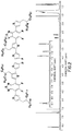
- FIG. 1 depicts a conventional device architecture and an inverted device architecture.
- FIG. 2 depicts 1 H of compound 2.
- FIG. 3 depicts 19 F NMR of compound 2.
- FIG. 4 depicts 1 H of compound 3.
- FIG. 5 depicts 19 F NMR of compound 3.
- FIG. 6 depicts Polymer F.
- FIG. 7 depicts the thin film UV-visible absorbance of Polymers A, B, C, D and E.
- FIG. 8 depicts the solution absorption measurements for Polymers A, B, C, and D.
- FIG. 9 depicts a comparison of the absorbance of films of Polymer A and Polymer F deposited from slot-die coating.
- Alkyl refers to an aliphatic hydrocarbon chains.
- the aliphatic hydrocarbon chains are of 1 to about 100 carbon atoms, preferably 1 to 30 carbon atoms, more preferably, 1 to 20 carbon atoms, and even more preferably, and includes straight and branched chains such as methyl, ethyl, n-propyl, isopropyl, n-butyl, isobutyl, sec-butyl, t-butyl, n-pentyl, isopentyl, neo-pentyl, n-hexyl, and isohexyl.
- alkyl groups can include the possibility of substituted and unsubstituted alkyl groups.
- Alkoxy refers to the group R—O— where R is an alkyl group of 1 to 100 carbon atoms.
- alkoxy groups can include the possibility of substituted and unsubstituted alkoxy groups.
- Aryl refers to an optionally substituted, mono-, di-, tri-, or other multicyclic aromatic ring system having from about 5 to about 50 carbon atoms (and all combinations and subcombinations of ranges and specific numbers of carbon atoms therein), with from about 6 to about 20 carbons being preferred.
- Non-limiting examples include, for example, phenyl, naphthyl, anthracenyl, and phenanthrenyl.
- Aryl groups can be optionally substituted with one or with one or more Rx.
- aryl groups can include the possibility of substituted aryl groups, bridged aryl groups and fused aryl groups.
- Ester represents a group of formula —COOR wherein R represents an “alkyl”, “aryl”, a “heterocycloalkyl” or “heteroaryl” moiety, or the same substituted as defined above
- Ketone represents an organic compound having a carbonyl group linked to a carbon atom such as —C(O)Rx wherein Rx can be alkyl, aryl, cycloalkyl, cycloalkenyl or heterocycle.
- “Amide” as used herein, represents a group of formula “—C(O)NR x R y ,” wherein R x and R y can be the same or independently H, alkyl, aryl, cycloalkyl, cycloalkenyl or heterocycle.
- the architecture When used as a photovoltaic device the architecture may be a conventional architecture device, while in others it may be an inverted architecture device.
- a conventional architecture device typically comprised of multilayered structure with a transparent anode as a substrate to collect positive charge (holes) and a cathode to collect negative charge (electrons), and a photo-active layer sandwiched in between two electrodes.
- An additional charge transport interlayer is inserted in between active layer and electrode for facile hole and electron transport.
- Each charge transport layer can be consisted of one or more layers.
- An inverted device has the same multilayered structure as the conventional architecture device whereas it uses a transparent cathode as a substrate to collect electrons and an anode to collect holes.
- the inverted device also has the photo-active layer and additional charge transport layers sandwiched in between two electrodes.
- FIG. 1 depicts a conventional device architecture and an inverted device architecture.
- the polymer can comprise:
- R 1 , R 4 , R 7 , and R 10 can be independently selected from H, or substituted, unsubstituted, straight-chain, branched, or cyclic alkyls ranging from about 1 to about 100 carbon atoms.
- R 1 , R 4 , R 7 , and R 10 can be identical to each other or in another variation R 1 , R 4 , R 7 , and R 10 can be different from each other.
- R 1 , R 4 , R 7 , and R 10 can be independently selected from unsubstituted branched alkyls ranging from about 1 to about 40 carbon atoms.
- R 2 , R 3 , R 5 , R 6 , R 8 and R 9 can be independently selected from F, Cl, S, H or CN or.
- R 2 , R 3 , R 5 , R 6 , R 8 and R 9 can be identical to each other or in another variation R 2 , R 3 , R 5 , R 6 , R 8 and R 9 can be different from each other.
- R 2 , R 3 , R 5 , R 6 , R 8 and R 9 can be F.
- R 11 and R 12 independently selected from H, substituted and unsubstituted aryls or, substituted, unsubstituted, straight-chain, branched, or cyclic alkyls ranging from about 1 to about 100 carbon atoms.
- R 11 and R 12 can be identical to each other or in another variation R 11 and R 12 can be different from each other.
- R 11 and R 12 can be selected from a branched thiophene with an unsubstituted branched alkyls ranging from about 1 to about 40 carbon atoms.
- the number of monomer units n in this polymer can range from about 1 to about 100,000 repeat units. In other features of this embodiment, the number of monomer units Z in this polymer can range from about 10 to about 75,000 repeat units, about 100 to about 50,000 repeat units or even from about 1,000 to about 20,000 repeat units.
- this polymer can be regio-regular or regio-random. It is also envisioned that the polymer can be used as a photovoltaic material or as an active layer in an electronic device.
- the polymer can comprise:
- n can range from about 1 to about 100,000 repeat units.
- the method of synthesizing the polymer begins by first generating the monomer.
- the method of synthesizing monomers can begin by coupling compound 1:
- the coupling can be any conventionally known coupling including Stille cross coupling, Suzuki cross coupling or direct arylation polymerization.
- X can be any known compound capable of coupling with the stannane. Non-limiting examples of X can be: Br, Cl, I, or even triflates.
- Y can be selected from the group consisting of Br, a stannyl groups (such as trimethyltin or tributyltin), a boronic ester (such as 4,4,5,5-tetramethyl-1,3,2-dioxaborolane, 1,3,2-dioxaborolane, or boronic acid) and a H.
- a stannyl groups such as trimethyltin or tributyltin
- a boronic ester such as 4,4,5,5-tetramethyl-1,3,2-dioxaborolane, 1,3,2-dioxaborolane, or boronic acid
- 5,5-Y-3,3′-difluoro-2,2′-bithiophene can be 3,3′-difluoro-[2,2′-bithiophene]-5,5′-diyl)bis(trimethylstannane).
- the coupling of compound 1 and 3,3′-difluoro-[2,2′-bithiophene]-5,5′-diyl)bis(trimethylstannane) occurs in the presence of a palladium catalyst.
- Non-limiting examples of the coupling procedure can involve taking compound 1 (0.65 g, 0.666 mmol), (3,3′-difluoro-[2,2′-bithiophene]-5,5′-diyl)bis(trimethylstannane) (0.16 g, 0.303 mmol), tri(o-toly)phosphine (0.015 g, 0.048 mmol), and tris(dibenzylideneacetone)dipalladium(0) (0.011 g, 0.012 mmol) and placing them in a dry Schlenk flask.
- the vessel can be evacuated and backfilled with argon three times.
- Anhydrous chlorobenzene 28 mL can be added and the mixture was heated to reflux.
- the resultant solution can be cooled to room temperature and the solvent can be evaporated under reduced pressure. The residue can then be eluted through a column.
- the compound 2
- the bromination can occur by taking compound 2 (0.47 g, 0.236 mmol) and dissolved it in anhydrous tetrahydrafuran (10 mL) in a dry Schlenk flask under argon. The solution was cooled to ⁇ 78° C. in a dry ice/2-propanol bath. N-Bromosuccinimide (0.167 g, 0.944 mmol) was dissolved in anhydrous tetrahydrafuran (5 mL) and added dropwise. The solution was wrapped in foil and stirred allowing the solution to be slowly warmed to room temperature. The solution was then precipitated with methanol and collected by filtration.
- the polymerization can be any conventionally known method of combining the monomers into a covalently bonded chain or network.
- compound 3 can be polymerized using Stille cross coupling, Suzuki cross coupling or direct arylation polymerization.
- the polymer When used in as an organic photovoltaic device the polymer can be used in conjunction with an anode.
- the anode for the organic photovoltaic device can be any conventionally known anode capable of operating as an organic photovoltaic device. Examples of anodes that can be used include: indium tin oxide, aluminum, silver, carbon, graphite, graphene, PEDOT:PSS, copper, metal nanowires, Zn 99 InO x , Zn 98 In 2 O x , Zn 97 In 3 O x , Zn 95 Mg 5 O x , Zn 90 Mg 10 O x , and Zn 85 Mg 15 O x .
- the polymer When used in as an organic photovoltaic device the polymer can be used in conjunction with a cathode.
- the cathode for the organic photovoltaic device can be any conventionally known cathode capable of operating as an organic photovoltaic device. Examples of cathodes that can be used include: indium tin oxide, carbon, graphite, graphene, PEDOT:PSS, copper, silver, aluminum, gold, metal nanowires.
- the copolymer When used in as an organic photovoltaic device the copolymer can be deposited onto an electron transport layer. Any commercially available electron transport layer can be used that is optimized for organic photovoltaic devices.
- the electron transport layer can comprise (AO x ) y BO (1-y) .
- (AO x ) y and BO (1-y) are metal oxides.
- a and B can be different metals selected to achieve ideal electron transport layers.
- A can be aluminum, indium, zinc, tin, copper, nickel, cobalt, iron, ruthenium, rhodium, osmium, tungsten, magnesium, indium, vanadium, titanium and molybdenum.
- B can be aluminum, indium, zinc, tin, copper, nickel, cobalt, iron, ruthenium, rhodium, osmium, tungsten, vanadium, titanium and molybdenum.
- Examples of (AO x ) y BO (1-y) include: (SnO x ) y ZnO (1-y) , (AlO x ) y ZnO (1-y) , (AlO x ) y InO z(1-y) , (AlO x ) y SnO z(1-y) , (AlO x ) y CuO z(1-y) , (AlO x ) y WO z(1-y) , (InO x ) y ZnO (1-y) , (InO x ) y SnO z(1-y) , (InO x ) y NiO z(1-y) , (ZnO x ) y CuO z(1-y) , (ZnO x ) y NiO z(1-y) , (ZnO x ) y FeO
- fullerene dopants can be combined with (AO x ) y BO (1-y) to make an electron transport layer for the organic photovoltaic device.
- fullerene dopants that can be combined include
- R′ can be selected from either N, O, S, C, or B.
- R′′ can be alkyl chains or substituted alkyl chains. Examples of substitutions for the substituted alkyl chains include halogens, N, Br, O, Si, or S. In one example R′′ can be selected from
- fullerene dopants that can be used include: [6,6]-phenyl-C 60 -butyric-N-(2-aminoethyl)acetamide, [6,6]-phenyl-C 60 -butyric-N-triethyleneglycol ester and [6,6]-phenyl-C 60 -butyric-N-2-dimethylaminoethyl ester.
- Zinc/tin oxide (ZTO):phenyl-C 60 -butyric-N-(2-hydroxyethyl)acetamide (PCBNOH) sol-gel solution was prepared by dissolving zinc acetate dihydrate or tin(II) acetate in 2-methoxyethanol and ethanolamine.
- the ZTO:PCBNOH sol-gel electron transport layer solution was prepared by mixing Zn(OAc) 2 (3.98 g), Sn(OAc) 2 (398 mg) and PCBNOH (20.0 mg) in 2-methoxyethanol (54 mL) with ethanolamine (996 ⁇ L). Solutions were then further diluted to 65 vol % by adding more 2-methoxyethanol and stirred for at least an hour before spin casting onto indium tin oxide substrate to form the electron transport layer.
- PCBNMI ZTO ([6,6]-phenyl-C 60 -butyric-N-2-trimethylammonium ethyl ester iodide
- One method of forming PCBNMI can be taking [6,6]-phenyl-C 60 -butyric-N-2-dimethylaminoethyl ester (0.05 g, 0.052 mmol) and dissolved it in dry THF (2 mL) under argon. Iodomethane (1.5 mL) was added in one portion and the vessel was sealed. The solution is then heated to 60° C. for 18 hours. The solution was cooled and opened to allow the liquids to evaporate.
- the polymer and the acceptor, PC 70 BM, in a ratio of 1:1.2 were dissolved in chlorobenzene at the concentration of 26 mg/mL to obtain the photoactive layer solution.
- the solution was stirred and heated at 80° C. overnight in a nitrogen filled glove box. The next day 3.0 vol % of 1,8-diiodooctane (DIO) was added before spin-coating of the photoactive layer.
- DIO 1,8-diiodooctane
- Indium tin oxide patterned glass substrates were cleaned by successive ultrasonications in acetone and isopropanol. Each 15-min step was repeated twice, and the freshly cleaned substrates were left to dry overnight at 60° C. Preceding fabrication, the substrates were further cleaned for 1.5 min in a UV-ozone chamber and the electron transport layer was immediately spin coated on top.
- Sol-gel electron transport layer solution was filtered directly onto the indium tin oxide with a 0.25 ⁇ m poly(vinylidene fluoride) filter and spin cast at 4000 rpm for 40 s. Films were then annealed at 170° C. for 15 min, and directly transferred into a nitrogen filled glove box.
- the photoactive layer was deposited on the electron transport layer via spin coating at 600 rpm for 40 s with the solution and the substrate being preheated at 110° C. and directly transferred into a glass petri dish for overnight solvent annealing.
- the substrates were loaded into the vacuum evaporator where MoO 3 (hole transport layer) and Ag (anode) were sequentially deposited by thermal evaporation. Deposition occurred at a pressure of ⁇ 4 ⁇ 10 ⁇ 6 torr. MoO 3 and Ag had thicknesses of 5.0 nm and 120 nm, respectively. Samples were then encapsulated with glass using an epoxy binder and treated with UV light for 3 min.
- the solution was heated to reflux then cooled and precipitated/suspended with acetone.
- the solid was filtered and subjected to Soxhlet extraction with acetone, followed by hexanes, followed by chloroform, and chlorobenzene.
- the chloroform and chlorobenzene extracts were concentrated by evaporating the solvent under reduced pressure and precipitating with acetone.
- the solid polymer A was collected by filtration and dried (88% yield).
- the solid was filtered into a paper thimble and subjected to Soxhlet extraction with acetone, followed by hexanes, followed by chloroform, and chlorobenzene.
- the chloroform and chlorobenzene extracts were concentrated by evaporating the solvent under reduced pressure and precipitating with acetone.
- the solid was collected by filtration and dried (75% yield).
- the vessel was evacuated and backfilled with argon. Anhydrous chlorobenzene was added, and the solution was freeze-pump-thawed. The solution was heated to reflux then cooled and precipitated/suspended with acetone. The solid was filtered into a paper thimble and subjected to Soxhlet extraction with acetone, followed by hexanes, followed by chloroform, and chlorobenzene. The chloroform and chlorobenzene extracts were concentrated by evaporating the solvent under reduced pressure and precipitating with acetone. The solid was collected by filtration and dried (80% yield).
- the vessel was evacuated and backfilled with argon. Anhydrous chlorobenzene was added, and the solution was freeze-pump-thawed. The solution was heated to reflux then cooled and precipitated/suspended with acetone. The solid was filtered into a paper thimble and subjected to Soxhlet extraction with acetone, followed by hexanes, followed by chloroform, and chlorobenzene. The chloroform and chlorobenzene extracts were concentrated by evaporating the solvent under reduced pressure and precipitating with acetone. The solid was collected by filtration and dried (85% yield).
- the mixture was placed under vacuum and backfilled with argon and 2.3 mL of anhydrous chlorobenzene was added.
- the solution was heated to 130° C. then cooled to room temperature.
- the product was precipitated by pouring the solution into methanol.
- the solid was purified by Soxhlet extraction, using acetone, hexane, dichloromethane and chloroform as the solvents. The portion obtained from chloroform was the main product (169 mg, yield 90.2%) after precipitation from methanol and then drying overnight.
- a 10 mg/mL solution of polymer was made by stirring the polymer in chlorobenzene at 80° C. for 18 hours. The solution was cooled to room temperature and deposited on glass by spin coating at 1200 rpm for 40 s. The film was dried under vacuum prior to absorption measurement. The thin film absorption spectra were acquired by using an Agilent Technologies 8453 spectrophotometer.
- FIG. 7 depicts the thin film UV-visible absorbance of Polymers A, B, C, D and E.
- FIG. 8 depicts the solution absorption of the polymers.
- Polymers A and F were tested in large area film deposition via slot-die coating. The following describes the fabrication process of films and large area photovoltaic cells.
- Zinc tin oxide (ZTO): phenyl-C 60 -butyric acid-2-N,N,N-trimethylammonium iodide ethyl ester (PCBNMI) sol-gel solutions were prepared by adding zinc acetate dihydrate (996 mg), tin (II) acetate (99.6 mg), and PCBNOH (5 mg) to 2-methoxyethanol (10 mL) and ethanolamine (249 ⁇ L). Solutions were stirred for a minimum of 8 hours before use.
- An Erichsen COATMASTER 510 was used to spread the electron transport layer on the large area ITO substrates.
- Approximately 300 ⁇ L of the zinc tin oxide:fullerene (ZTO:PCBNMI) sol-gel solution was drawn into a pipette and deposited without filtration, directly onto the ITO at room temperature.
- a blade, with a gap height set at 300 ⁇ m, was then drawn through the ZTO:PCBNMI solution and across the ITO at a printing speed of 20 mm/s to create a uniform film on the substrate.
- the films were air dried for 15 min before the substrates were removed from the chuck and annealed at 170° C. for 15 min.
- the deposited film dimension was 8 ⁇ 10 cm.
- the photoactive layer consisted of either donor polymer Example 1 or 6 and acceptor [6,6]-phenyl-C 70 -butyric acid methyl ester (PCBM). While the examples illustrate an acceptor of PCBM it has been shown that any type of fullerene or non-fullerene acceptor can be used.
- non-fullerene acceptors like 3,9-bis(2-methylene-(3-(1,1-dicyanomethylene)-indanone))-5,5,11,11-tetrakis(4-hexylphenyl)-dithieno[2,3-d:2′,3′-d′]-s-indaceno[1,2-b:5,6-b′]dithiophene (ITIC) and 3,9-bis(2-methylene-((3-(1,1-dicyanomethylene)-6,7-difluoro)-indanone))-5,5,11,11-tetrakis(4-hexylphenyl)-dithieno[2,3-d:2′,3′-d′ ]-s-indaceno[1,2-b:5,6-b′]dithiophene (ITIC-DF) can be used.
- Example 1 the ink concentration was 26 mg/mL in 1:1 chlorobenzene:dichlorobenzene with 3 vol % 1,2,4-trichlorobenzene.
- Example 6 the ink concentration was 24 mg/mL in 1:1 1,2-dichlorobenzene and 1,2,4-trichlorobenzene. Both solutions were stirred and heated to 110° C. for a minimum of 18 hours. Solutions were cooled to room temperature immediately before using. No filtration was performed.
- An FOM Technologies-Compact Sheet Coater was used to slot-die coat the photoactive layer onto the electron transport layer on ITO substrates.
- the photoactive layer solution was stirred and heated to 110° C. for a minimum of 30 min before drawing several mL through a 1/16′′ ID FEP tube and into a 5 mL luer lock syringe without filtration.
- the syringe was placed into the slot-die pump at a syringe diameter setting of 36 mm and the tube was connected to the blade feed.
- the 1.3 cm wide blade was positioned above the substrate.
- the coating was performed at 45° C.
- the coating was performed at 90° C. with a 250 ⁇ m gap height, 150 cm/min coating speed and 0.5 mL/min syringe pump speed.
- the photoactive layer films were allowed to anneal at the substrate deposition temperature until dry. All films were deposited and annealed in ambient air. The deposited film dimensions were 1.3 ⁇ 10 cm.
- FIG. 9 A comparison of the absorbance of films of Polymer A and Polymer F deposited from slot-die coating are shown on FIG. 9 .
- Films deposited with the Polymer F have crystallites in the film and areas where the film has dewetted. They areas are likely to lead to electrical shorting in devices and reduce photovoltaic performance. Polymer F appeared to have a greater extent of intermolecular ordering compared to Polymer A.
- the substrates were immediately loaded into a Kurt J. Lesker Nano 36 Thin Film Deposition System vacuum evaporator where a mask was fitted to produce three individual devices per substrate.
- a MoO x (hole transport layer) and Ag (anode) were sequentially deposited by thermal evaporation.
- the MoO x was evaporated from an Al 2 O 3 crucible supported by a W basket to a final thickness of 3.5 nm.
- the Ag was evaporated from a W boat to a final thickness of 120 nm. Deposition occurred at a pressure of 2 ⁇ 10-6 torr.
- the deposition rates, 0.5-0.8 ⁇ /s for the MoO 3 and 1.5-2.0 ⁇ /s for the Ag, and the final film thicknesses were determined by a Kurt J. Lesker FTM 2400 crystal monitor.
- Devices were tested under AM 1.5 G 100 mW/cm 2 conditions with a Newport Thermal Oriel 91192 1000 W solar simulator (4′′ ⁇ 4′′ illumination size).
- the active area of the devices was determined by measuring the dimensions of the ITO covered by electron transport layer, photoactive layer, hole transport layer and Ag. The device area is 0.1 cm 2 .
- the current density-voltage curves were measured using a Keithley 2400 source meter and voltage scans were taken from ⁇ 1 V to 2 V.
- the light intensity was calibrated with a crystalline silicon reference photovoltaic fitted with a KG-5 filter (calibrated by Newport to minimize spectral mismatch).
- Jsc Short-circuit current density
- V oc V
- Open-circuit voltage V oc
- Fill factor percentage FF % is the ratio of the maximum power point divided by the open circuit voltage and the short circuit current.
- PCE % The power conversion efficiency (PCE) of a photovoltaic cell is the percentage of the solar energy shining on a photovoltaic device that is converted into usable electricity.
- Photoactive layer films containing either Polymer A or Polymer F with PCBM or ITIC-DF were slot-die coated onto ZTO:PCBNMI ETL-coated ITO substrates that were heated to 45° C.
- Polymer:PCBM solutions were prepared at a ratio of 1:1.6 in a 1:1 mixture of chlorobenzene:dichlorobenzene with a 3 vol % 1,2,4-trichlorobenzene additive.
- the total concentration was 26 mg/ml.
- solutions containing Polymer F the total concentration was 24 mg/ml.
- Polymer:ITIC-DF solutions were prepared using a 1:1 ratio in chlorobenzene with a 3 vol % 1,2,4-trichlorobenzene additive.
- solutions containing Polymer A the total concentration was 24 mg/ml
- solutions containing Polymer F the total concentration was 20 mg/ml. All solutions were heated to 80° C. and stirred overnight to dissolve the polymer and acceptor. The solutions were cooled to room temperature before use.
- the Polymer A:PCBM solutions were slot-die coated using a gap height of 250 ⁇ m, a coating speed of 150 cm/min, and a pump speed of 0.5 ml/min.
- the Polymer F:PCBM solutions were slot-die coated using a gap height of 100 ⁇ m, a coating speed of 25 cm/min, and a pump speed of 0.02 ml/min.
- the Polymer A:ITIC-DF solutions were slot-die coated using a gap height of 100 ⁇ m, a coating speed of 8 cm/min, and a pump speed of 0.02 ml/min.
- the Polymer F:ITIC-DF solutions were slot-die coated using a gap height of 200 ⁇ m, a coating speed of 25 cm/min, and a pump speed of 0.02 ml/min.
- Jsc Short-circuit current density
- V oc V
- Open-circuit voltage V oc
- Fill factor percentage FF % is the ratio of the maximum power point divided by the open circuit voltage and the short circuit current.
- PCE % The power conversion efficiency (PCE) of a photovoltaic cell is the percentage of the solar energy shining on a photovoltaic device that is converted into usable electricity.
- ITO coated glass substrates (8-12 ⁇ ) were acquired from Thin Film Devices and cleaned with 15 min ultrasonications successively in acetone, and 2-propanol. The substrates were dried in an oven at 60° C. for at least 2 h. Immediately before use, substrates were further cleaned for 1.5 min with a UV-ozone cleaner.
- ITO indium tin oxide
- a ZTO:PCBNMI sol-gel solution was made by adding 1 g of zinc acetate dihydrate (Zn(OAc) 2 ), Sn(OAc) 2 (0.1 g), and 5 mg of PCBNMI to a vial. To the vial was added 249 ⁇ L of ethanolamine and 10 mL of anhydrous 2-methoxyethanol. The solution was stirred at room temperature for at least 24 hours. The solution was filtered with a 0.2 ⁇ m polytetrafluoroethylene (PTFE) syringe filter directly onto a freshly cleaned ITO substrate.
- ZTO:PCBNMI was spin-cast at 4000 rpm for 40 s and annealed at 170° C. for 15 min in air to form rigid electron transport layer. The substrates were then transferred into a nitrogen filled glovebox.
- the photoactive layer was spin-cast onto the ZTO:PCBNMI ETL coated ITO substrates at 400-1000 rpm for 40 s. The substrates were immediately removed from the spin-coating chuck and placed in a closed glass petri dish for 1 h. The film covering the ITO contact was scratched away, and the devices were loaded into the thermal evaporation chamber.
- Evaporation was performed at a pressure of ⁇ 4 ⁇ 10 ⁇ 6 mbar.
- 3.5 nm of MoO 3 was deposited at 0.4-0.6 ⁇ /s, and 120 nm of Ag was deposited at 1.5-2.0 ⁇ /s.
- the devices were encapsulated with UV-curable epoxy and sealed with a glass slide, and exposed to UV light for 3 min.
- Table 3 depicts the small area photovoltaic performance of Polymers A-F.
Abstract

and 5,5-Y-3,3′-difluoro-2,2′-bithiophene to produce

-
- wherein X can be any known compound capable of coupling with the Y-difluorothiophene and Y is selected from the group consisting of Br, a stannyl group, a boronic ester and a H.
Description

and 5,5-Y-3,3′-difluoro-2,2′-bithiophene to produce


and 3,3′-difluoro-[2,2′-bithiophene]-5,5′-diyl)bis(trimethylstannane) to produce

The method then brominates

to produce

This is followed by polymerizing

to produce

wherein n ranges from 1 to 100,000 repeat units.


and 5,5-Y-3,3′-difluoro-2,2′-bithiophene. The coupling can be any conventionally known coupling including Stille cross coupling, Suzuki cross coupling or direct arylation polymerization. In compound 1, X can be any known compound capable of coupling with the stannane. Non-limiting examples of X can be: Br, Cl, I, or even triflates. Y can be selected from the group consisting of Br, a stannyl groups (such as trimethyltin or tributyltin), a boronic ester (such as 4,4,5,5-tetramethyl-1,3,2-dioxaborolane, 1,3,2-dioxaborolane, or boronic acid) and a H. Other more non-limiting specific examples of 5,5-Y-3,3′-difluoro-2,2′-bithiophene can be 3,3′-difluoro-[2,2′-bithiophene]-5,5′-diyl)bis(trimethylstannane).

can then be further purified by recrystallization to yield the product as a red wax (0.28 g, 46% yield). The 1H and 19F NMRs are shown in


and [6,6]-phenyl-C60-butyric-N-2-trimethylammonium ethyl ester iodide.

R′ can be selected from either N, O, S, C, or B. In other embodiment R″ can be alkyl chains or substituted alkyl chains. Examples of substitutions for the substituted alkyl chains include halogens, N, Br, O, Si, or S. In one example R″ can be selected from

Other examples of fullerene dopants that can be used include: [6,6]-phenyl-C60-butyric-N-(2-aminoethyl)acetamide, [6,6]-phenyl-C60-butyric-N-triethyleneglycol ester and [6,6]-phenyl-C60-butyric-N-2-dimethylaminoethyl ester.


tri(o-toly)phosphine (1.8 mg, 6.0 μmol), and tris(dibenzylideneacetone)dipalladium(0) (1.4 mg, 2.0 μmol) were placed in a dry Schlenk flask. The vessel was evacuated and backfilled with argon. Anhydrous chlorobenzene was added, and the solution was freeze-pump-thawed. The solution was heated to reflux then cooled and precipitated/suspended with acetone. The solid was filtered into a paper thimble and subjected to Soxhlet extraction with acetone, followed by hexanes, followed by chloroform, and chlorobenzene. The chloroform and chlorobenzene extracts were concentrated by evaporating the solvent under reduced pressure and precipitating with acetone. The solid was collected by filtration and dried (41% yield).
| TABLE 1 | ||||
| Photoactive Layer | Voc (V) | Jsc (mA/cm2) | FF (%) | PCE (%) |
| Polymer F: PCBM | 0.70 | 19.3 | 53.4 | 7.3 |
| Polymer A: PCBM | 0.79 | 19.1 | 55.5 | 8.3 |
| TABLE 2 | ||||
| Efficiency | ||||
| Photoactive Layer | VOC (V) | JSC (mA/cm2) | FF (%) | (%) |
| Polymer A: PCBM | 0.830 | 9.7 | 63.0 | 4.6 |
| Polymer F: PCBM | — | — | — | — |
| Polymer A: ITIC-DF | 0.812 | 18.2 | 55.6 | 8.0 |
| Polymer F: ITIC-DF | 0.784 | 11.8 | 45.8 | 4.3 |
| TABLE 3 | ||||
| Jsc | Voc (V) | FF (%) | ||
| PCE (%) | (mA/cm2) | Aver- | Aver- |
| Device | Average | Max | Average | Max | age | Max | age | Max |
| Polymer A | 11.5 | 11.8 | 19.0 | 19.5 | 0.820 | 0.827 | 73.9 | 75.0 |
| Polymer B | 5.26 | 5.67 | 10.10 | 11.20 | 0.760 | 0.778 | 68.6 | 70.8 |
| Polymer C | 7.26 | 7.77 | 12.90 | 13.60 | 0.820 | 0.829 | 68.6 | 70.8 |
| Polymer D | 7.94 | 8.29 | 15.04 | 16.16 | 0.828 | 0.832 | 63.8 | 66.6 |
| Polymer E | 7.29 | 7.43 | 12.80 | 13.30 | 0.778 | 0.781 | 73.4 | 74.6 |
| Polymer F | 11.89 | 12.04 | 19.82 | 20.18 | 0.805 | 0.810 | 74.6 | 75.8 |
Claims (10)


Priority Applications (1)
| Application Number | Priority Date | Filing Date | Title |
|---|---|---|---|
| US16/253,992 US10787537B2 (en) | 2018-01-29 | 2019-01-22 | Synthesis of polymers for organic photovoltaics |
Applications Claiming Priority (2)
| Application Number | Priority Date | Filing Date | Title |
|---|---|---|---|
| US201862623274P | 2018-01-29 | 2018-01-29 | |
| US16/253,992 US10787537B2 (en) | 2018-01-29 | 2019-01-22 | Synthesis of polymers for organic photovoltaics |
Publications (2)
| Publication Number | Publication Date |
|---|---|
| US20190233577A1 US20190233577A1 (en) | 2019-08-01 |
| US10787537B2 true US10787537B2 (en) | 2020-09-29 |
Family
ID=67392747
Family Applications (1)
| Application Number | Title | Priority Date | Filing Date |
|---|---|---|---|
| US16/253,992 Active 2039-03-01 US10787537B2 (en) | 2018-01-29 | 2019-01-22 | Synthesis of polymers for organic photovoltaics |
Country Status (1)
| Country | Link |
|---|---|
| US (1) | US10787537B2 (en) |
Families Citing this family (1)
| Publication number | Priority date | Publication date | Assignee | Title |
|---|---|---|---|---|
| WO2020018257A1 (en) * | 2018-07-16 | 2020-01-23 | Phillips 66 Company | Polymers containing 3'-(alkoxy)-[2,2'-bithiophene]-3carbonitrile for high performance organic photovoltaics |
Citations (3)
| Publication number | Priority date | Publication date | Assignee | Title |
|---|---|---|---|---|
| US20110240973A1 (en) * | 2010-03-31 | 2011-10-06 | Basf Se | Annellated Dithiophene Copolymers |
| US20140312317A1 (en) * | 2013-04-19 | 2014-10-23 | Au Optronics Corporation | Organic semiconductor material and thin-film transistor |
| US20170301862A1 (en) * | 2014-10-22 | 2017-10-19 | The Hong Kong University Of Science And Technology | Difluorobithiophene-Based Donor-Acceptor Polymers for Electronic and Photonic Applications |
-
2019
- 2019-01-22 US US16/253,992 patent/US10787537B2/en active Active
Patent Citations (3)
| Publication number | Priority date | Publication date | Assignee | Title |
|---|---|---|---|---|
| US20110240973A1 (en) * | 2010-03-31 | 2011-10-06 | Basf Se | Annellated Dithiophene Copolymers |
| US20140312317A1 (en) * | 2013-04-19 | 2014-10-23 | Au Optronics Corporation | Organic semiconductor material and thin-film transistor |
| US20170301862A1 (en) * | 2014-10-22 | 2017-10-19 | The Hong Kong University Of Science And Technology | Difluorobithiophene-Based Donor-Acceptor Polymers for Electronic and Photonic Applications |
Non-Patent Citations (2)
| Title |
|---|
| El-Shehawy et al. "Alternating Copolymers Based on 2,1,3-Benzothiadiazole and Hexylthiophene: Positioning Effect of Hexyl Chains on the Photophysical and Electrochemical Properties", European Journal of Organic Chemistry. 2011, pp. 2841-4852; PDF available from Wiley Online Library. (Year: 2011). * |
| Lee et al. "Two-Dimensionally Extended π-Conjugation of Donor-Acceptor Copolymers via Oligothienyl Side Chains for Efficient Polymer Solar Cells", Macromolecules 2015, pp. 1723-1735; PDF available from ACS Publications. (Year: 2015). * |
Also Published As
| Publication number | Publication date |
|---|---|
| US20190233577A1 (en) | 2019-08-01 |
Similar Documents
| Publication | Publication Date | Title |
|---|---|---|
| EP3658600A1 (en) | High performance wide-bandgap polymers for organic photovoltaics | |
| US10714270B2 (en) | Photoelectric conversion device and method for manufacturing the same | |
| US10787538B2 (en) | Polymers for organic photovoltaics | |
| KR20120130706A (en) | Electron donating polymer and solar cell including the same | |
| US10361370B2 (en) | Unsymmetrical benzothiadiazole-based molecular complexes in organic photovoltaic devices | |
| US10787537B2 (en) | Synthesis of polymers for organic photovoltaics | |
| US11332579B1 (en) | Fused dithieno benzothiadiazole polymers for organic photovoltaics | |
| US11091585B2 (en) | Polymers containing 3′-(alkoxy)-[2,2′-bithiophene]-3-carbonitrile for high performance organic photovoltaics | |
| US20220363813A1 (en) | Repeat units for photovoltaic applications | |
| US20220372190A1 (en) | Monomers for photovoltaic applications | |
| US20220359827A1 (en) | Polymers for photovoltaic applications | |
| US11690283B2 (en) | Fused dithieno benzothiadiazole polymers for organic photovoltaics | |
| US20220380494A1 (en) | Polymers for photovoltaic applications | |
| US10804468B2 (en) | Unsymmetrical benzo[1,2-b:4,5-b′]dithiophene and benzothiadiazole-based molecular complexes | |
| US10647851B2 (en) | 1,2,5,6-Naphthalenediimide co-polymer | |
| US11326019B1 (en) | Fused dithieno benzothiadiazole polymers for organic photovoltaics | |
| US11849629B2 (en) | Fused dithieno benzothiadiazole polymers for organic photovolatics | |
| US20230086615A1 (en) | Forming ester-substituted polymers for organic photovoltaics | |
| US20230094872A1 (en) | Ester-substituted polymers for organic photovoltaics | |
| US11274178B2 (en) | High performance wide-bandgap polymers for organic photovoltaics | |
| US11639421B2 (en) | Unsymmetrical benzothtadiazole-based random copolymers | |
| US11228000B2 (en) | Organic semiconducting polymers | |
| US20210238344A1 (en) | Unsymmetrical benzothiadiazole-based random copolymers | |
| JP7182606B2 (en) | High Performance Wide Bandgap Polymers for Organic Photovoltaics | |
| US20210246261A1 (en) | Unsymmetrical benzothiadiazole-based random copolymers |
Legal Events
| Date | Code | Title | Description |
|---|---|---|---|
| FEPP | Fee payment procedure |
Free format text: ENTITY STATUS SET TO UNDISCOUNTED (ORIGINAL EVENT CODE: BIG.); ENTITY STATUS OF PATENT OWNER: LARGE ENTITY |
|
| AS | Assignment |
Owner name: PHILLIPS 66 COMPANY, TEXAS Free format text: ASSIGNMENT OF ASSIGNORS INTEREST;ASSIGNORS:BULLOCK, JOE;WORFOLK, BRIAN;EARMME, TAESHIK;AND OTHERS;SIGNING DATES FROM 20190128 TO 20190214;REEL/FRAME:048360/0259 |
|
| STPP | Information on status: patent application and granting procedure in general |
Free format text: NON FINAL ACTION MAILED |
|
| STPP | Information on status: patent application and granting procedure in general |
Free format text: PUBLICATIONS -- ISSUE FEE PAYMENT VERIFIED |
|
| STCF | Information on status: patent grant |
Free format text: PATENTED CASE |
|
| MAFP | Maintenance fee payment |
Free format text: PAYMENT OF MAINTENANCE FEE, 4TH YEAR, LARGE ENTITY (ORIGINAL EVENT CODE: M1551); ENTITY STATUS OF PATENT OWNER: LARGE ENTITY Year of fee payment: 4 |