US10784458B1 - Organic light-emitting diode with enhanced light-emitting efficiency and color purity - Google Patents
Organic light-emitting diode with enhanced light-emitting efficiency and color purity Download PDFInfo
- Publication number
- US10784458B1 US10784458B1 US16/354,826 US201916354826A US10784458B1 US 10784458 B1 US10784458 B1 US 10784458B1 US 201916354826 A US201916354826 A US 201916354826A US 10784458 B1 US10784458 B1 US 10784458B1
- Authority
- US
- United States
- Prior art keywords
- layer
- sensitizer
- luminescent
- emitting diode
- organic light
- Prior art date
- Legal status (The legal status is an assumption and is not a legal conclusion. Google has not performed a legal analysis and makes no representation as to the accuracy of the status listed.)
- Active
Links
- 239000000463 material Substances 0.000 claims abstract description 97
- 230000005283 ground state Effects 0.000 claims description 14
- 230000000903 blocking effect Effects 0.000 claims description 11
- 230000005525 hole transport Effects 0.000 claims description 9
- 239000002019 doping agent Substances 0.000 claims description 8
- TVIVIEFSHFOWTE-UHFFFAOYSA-K tri(quinolin-8-yloxy)alumane Chemical compound [Al+3].C1=CN=C2C([O-])=CC=CC2=C1.C1=CN=C2C([O-])=CC=CC2=C1.C1=CN=C2C([O-])=CC=CC2=C1 TVIVIEFSHFOWTE-UHFFFAOYSA-K 0.000 claims description 8
- 150000001454 anthracenes Chemical class 0.000 claims description 4
- 229910052741 iridium Inorganic materials 0.000 claims description 4
- GKOZUEZYRPOHIO-UHFFFAOYSA-N iridium atom Chemical compound [Ir] GKOZUEZYRPOHIO-UHFFFAOYSA-N 0.000 claims description 4
- HDMYKJVSQIHZLM-UHFFFAOYSA-N 1-[3,5-di(pyren-1-yl)phenyl]pyrene Chemical compound C1=CC(C=2C=C(C=C(C=2)C=2C3=CC=C4C=CC=C5C=CC(C3=C54)=CC=2)C=2C3=CC=C4C=CC=C5C=CC(C3=C54)=CC=2)=C2C=CC3=CC=CC4=CC=C1C2=C43 HDMYKJVSQIHZLM-UHFFFAOYSA-N 0.000 claims description 3
- 239000005725 8-Hydroxyquinoline Substances 0.000 claims description 3
- 150000004696 coordination complex Chemical class 0.000 claims description 3
- 229960003540 oxyquinoline Drugs 0.000 claims description 3
- MCJGNVYPOGVAJF-UHFFFAOYSA-N quinolin-8-ol Chemical compound C1=CN=C2C(O)=CC=CC2=C1 MCJGNVYPOGVAJF-UHFFFAOYSA-N 0.000 claims description 3
- OBAJPWYDYFEBTF-UHFFFAOYSA-N 2-tert-butyl-9,10-dinaphthalen-2-ylanthracene Chemical compound C1=CC=CC2=CC(C3=C4C=CC=CC4=C(C=4C=C5C=CC=CC5=CC=4)C4=CC=C(C=C43)C(C)(C)C)=CC=C21 OBAJPWYDYFEBTF-UHFFFAOYSA-N 0.000 claims description 2
- VIZUPBYFLORCRA-UHFFFAOYSA-N 9,10-dinaphthalen-2-ylanthracene Chemical compound C12=CC=CC=C2C(C2=CC3=CC=CC=C3C=C2)=C(C=CC=C2)C2=C1C1=CC=C(C=CC=C2)C2=C1 VIZUPBYFLORCRA-UHFFFAOYSA-N 0.000 claims description 2
- SXGIRTCIFPJUEQ-UHFFFAOYSA-N 9-anthracen-9-ylanthracene Chemical compound C1=CC=CC2=CC3=CC=CC=C3C(C=3C4=CC=CC=C4C=C4C=CC=CC4=3)=C21 SXGIRTCIFPJUEQ-UHFFFAOYSA-N 0.000 claims description 2
- MWPLVEDNUUSJAV-LSMJWXKXSA-N anthracene Chemical compound [13CH]1=[13CH][13CH]=[13CH][13C]2=CC3=CC=CC=C3C=[13C]21 MWPLVEDNUUSJAV-LSMJWXKXSA-N 0.000 claims description 2
- MWPLVEDNUUSJAV-UHFFFAOYSA-N anthracene Natural products C1=CC=CC2=CC3=CC=CC=C3C=C21 MWPLVEDNUUSJAV-UHFFFAOYSA-N 0.000 claims description 2
- GQVWHWAWLPCBHB-UHFFFAOYSA-L beryllium;benzo[h]quinolin-10-olate Chemical compound [Be+2].C1=CC=NC2=C3C([O-])=CC=CC3=CC=C21.C1=CC=NC2=C3C([O-])=CC=CC3=CC=C21 GQVWHWAWLPCBHB-UHFFFAOYSA-L 0.000 claims description 2
- 230000003111 delayed effect Effects 0.000 claims description 2
- 125000002080 perylenyl group Chemical group C1(=CC=C2C=CC=C3C4=CC=CC5=CC=CC(C1=C23)=C45)* 0.000 claims description 2
- 150000003220 pyrenes Chemical class 0.000 claims description 2
- LVTJYYZZSDQQPE-UHFFFAOYSA-N 1-(2,5-dimethyl-4-pyren-1-ylphenyl)pyrene Chemical compound C1=C2C(C=3C=C(C(=CC=3C)C=3C4=CC=C5C=CC=C6C=CC(C4=C65)=CC=3)C)=CC=C(C=C3)C2=C2C3=CC=CC2=C1 LVTJYYZZSDQQPE-UHFFFAOYSA-N 0.000 claims 2
- 230000000052 comparative effect Effects 0.000 description 17
- UEEXRMUCXBPYOV-UHFFFAOYSA-N iridium;2-phenylpyridine Chemical compound [Ir].C1=CC=CC=C1C1=CC=CC=N1.C1=CC=CC=C1C1=CC=CC=N1.C1=CC=CC=C1C1=CC=CC=N1 UEEXRMUCXBPYOV-UHFFFAOYSA-N 0.000 description 9
- 230000007246 mechanism Effects 0.000 description 9
- 238000010586 diagram Methods 0.000 description 5
- 239000000243 solution Substances 0.000 description 5
- 230000002708 enhancing effect Effects 0.000 description 4
- 238000005286 illumination Methods 0.000 description 4
- 230000001965 increasing effect Effects 0.000 description 4
- 230000006798 recombination Effects 0.000 description 4
- 238000005215 recombination Methods 0.000 description 4
- 238000005401 electroluminescence Methods 0.000 description 3
- 230000001052 transient effect Effects 0.000 description 3
- QBFQLEVWHCQDIR-UHFFFAOYSA-N 1-(2,4-dimethylphenyl)-2-pyrrolidin-1-ylpropan-1-one Chemical compound CC1=C(C=CC(=C1)C)C(C(C)N1CCCC1)=O QBFQLEVWHCQDIR-UHFFFAOYSA-N 0.000 description 2
- 230000000694 effects Effects 0.000 description 2
- 238000004770 highest occupied molecular orbital Methods 0.000 description 2
- 238000004768 lowest unoccupied molecular orbital Methods 0.000 description 2
- BBEAQIROQSPTKN-UHFFFAOYSA-N pyrene Chemical compound C1=CC=C2C=CC3=CC=CC4=CC=C1C2=C43 BBEAQIROQSPTKN-UHFFFAOYSA-N 0.000 description 2
- 230000004044 response Effects 0.000 description 2
- 230000001960 triggered effect Effects 0.000 description 2
- DHDHJYNTEFLIHY-UHFFFAOYSA-N 4,7-diphenyl-1,10-phenanthroline Chemical compound C1=CC=CC=C1C1=CC=NC2=C1C=CC1=C(C=3C=CC=CC=3)C=CN=C21 DHDHJYNTEFLIHY-UHFFFAOYSA-N 0.000 description 1
- UHBIKXOBLZWFKM-UHFFFAOYSA-N 8-hydroxy-2-quinolinecarboxylic acid Chemical compound C1=CC=C(O)C2=NC(C(=O)O)=CC=C21 UHBIKXOBLZWFKM-UHFFFAOYSA-N 0.000 description 1
- FJNCXZZQNBKEJT-UHFFFAOYSA-N 8beta-hydroxymarrubiin Natural products O1C(=O)C2(C)CCCC3(C)C2C1CC(C)(O)C3(O)CCC=1C=COC=1 FJNCXZZQNBKEJT-UHFFFAOYSA-N 0.000 description 1
- GYHNNYVSQQEPJS-UHFFFAOYSA-N Gallium Chemical compound [Ga] GYHNNYVSQQEPJS-UHFFFAOYSA-N 0.000 description 1
- 239000007983 Tris buffer Substances 0.000 description 1
- 229910052782 aluminium Inorganic materials 0.000 description 1
- 239000004411 aluminium Substances 0.000 description 1
- 230000015556 catabolic process Effects 0.000 description 1
- 238000006731 degradation reaction Methods 0.000 description 1
- GVEPBJHOBDJJJI-UHFFFAOYSA-N fluoranthrene Natural products C1=CC(C2=CC=CC=C22)=C3C2=CC=CC3=C1 GVEPBJHOBDJJJI-UHFFFAOYSA-N 0.000 description 1
- 229910052733 gallium Inorganic materials 0.000 description 1
- 230000014509 gene expression Effects 0.000 description 1
- 230000006872 improvement Effects 0.000 description 1
- AMGQUBHHOARCQH-UHFFFAOYSA-N indium;oxotin Chemical compound [In].[Sn]=O AMGQUBHHOARCQH-UHFFFAOYSA-N 0.000 description 1
- 230000004048 modification Effects 0.000 description 1
- 238000012986 modification Methods 0.000 description 1
- IBHBKWKFFTZAHE-UHFFFAOYSA-N n-[4-[4-(n-naphthalen-1-ylanilino)phenyl]phenyl]-n-phenylnaphthalen-1-amine Chemical compound C1=CC=CC=C1N(C=1C2=CC=CC=C2C=CC=1)C1=CC=C(C=2C=CC(=CC=2)N(C=2C=CC=CC=2)C=2C3=CC=CC=C3C=CC=2)C=C1 IBHBKWKFFTZAHE-UHFFFAOYSA-N 0.000 description 1
- 125000001997 phenyl group Chemical group [H]C1=C([H])C([H])=C(*)C([H])=C1[H] 0.000 description 1
- 230000000171 quenching effect Effects 0.000 description 1
Images


Classifications
-
- H01L51/504—
-
- H—ELECTRICITY
- H10—SEMICONDUCTOR DEVICES; ELECTRIC SOLID-STATE DEVICES NOT OTHERWISE PROVIDED FOR
- H10K—ORGANIC ELECTRIC SOLID-STATE DEVICES
- H10K50/00—Organic light-emitting devices
- H10K50/10—OLEDs or polymer light-emitting diodes [PLED]
- H10K50/11—OLEDs or polymer light-emitting diodes [PLED] characterised by the electroluminescent [EL] layers
-
- H01L51/0058—
-
- H01L51/0081—
-
- H01L51/5004—
-
- H01L51/5056—
-
- H01L51/5072—
-
- H01L51/5096—
-
- H—ELECTRICITY
- H10—SEMICONDUCTOR DEVICES; ELECTRIC SOLID-STATE DEVICES NOT OTHERWISE PROVIDED FOR
- H10K—ORGANIC ELECTRIC SOLID-STATE DEVICES
- H10K50/00—Organic light-emitting devices
- H10K50/10—OLEDs or polymer light-emitting diodes [PLED]
- H10K50/11—OLEDs or polymer light-emitting diodes [PLED] characterised by the electroluminescent [EL] layers
- H10K50/12—OLEDs or polymer light-emitting diodes [PLED] characterised by the electroluminescent [EL] layers comprising dopants
- H10K50/121—OLEDs or polymer light-emitting diodes [PLED] characterised by the electroluminescent [EL] layers comprising dopants for assisting energy transfer, e.g. sensitization
-
- H—ELECTRICITY
- H10—SEMICONDUCTOR DEVICES; ELECTRIC SOLID-STATE DEVICES NOT OTHERWISE PROVIDED FOR
- H10K—ORGANIC ELECTRIC SOLID-STATE DEVICES
- H10K50/00—Organic light-emitting devices
- H10K50/10—OLEDs or polymer light-emitting diodes [PLED]
- H10K50/11—OLEDs or polymer light-emitting diodes [PLED] characterised by the electroluminescent [EL] layers
- H10K50/125—OLEDs or polymer light-emitting diodes [PLED] characterised by the electroluminescent [EL] layers specially adapted for multicolour light emission, e.g. for emitting white light
- H10K50/13—OLEDs or polymer light-emitting diodes [PLED] characterised by the electroluminescent [EL] layers specially adapted for multicolour light emission, e.g. for emitting white light comprising stacked EL layers within one EL unit
-
- H—ELECTRICITY
- H10—SEMICONDUCTOR DEVICES; ELECTRIC SOLID-STATE DEVICES NOT OTHERWISE PROVIDED FOR
- H10K—ORGANIC ELECTRIC SOLID-STATE DEVICES
- H10K50/00—Organic light-emitting devices
- H10K50/10—OLEDs or polymer light-emitting diodes [PLED]
- H10K50/14—Carrier transporting layers
- H10K50/15—Hole transporting layers
-
- H—ELECTRICITY
- H10—SEMICONDUCTOR DEVICES; ELECTRIC SOLID-STATE DEVICES NOT OTHERWISE PROVIDED FOR
- H10K—ORGANIC ELECTRIC SOLID-STATE DEVICES
- H10K50/00—Organic light-emitting devices
- H10K50/10—OLEDs or polymer light-emitting diodes [PLED]
- H10K50/14—Carrier transporting layers
- H10K50/16—Electron transporting layers
-
- H—ELECTRICITY
- H10—SEMICONDUCTOR DEVICES; ELECTRIC SOLID-STATE DEVICES NOT OTHERWISE PROVIDED FOR
- H10K—ORGANIC ELECTRIC SOLID-STATE DEVICES
- H10K85/00—Organic materials used in the body or electrodes of devices covered by this subclass
- H10K85/60—Organic compounds having low molecular weight
- H10K85/615—Polycyclic condensed aromatic hydrocarbons, e.g. anthracene
- H10K85/626—Polycyclic condensed aromatic hydrocarbons, e.g. anthracene containing more than one polycyclic condensed aromatic rings, e.g. bis-anthracene
-
- H—ELECTRICITY
- H10—SEMICONDUCTOR DEVICES; ELECTRIC SOLID-STATE DEVICES NOT OTHERWISE PROVIDED FOR
- H10K—ORGANIC ELECTRIC SOLID-STATE DEVICES
- H10K2101/00—Properties of the organic materials covered by group H10K85/00
- H10K2101/10—Triplet emission
-
- H—ELECTRICITY
- H10—SEMICONDUCTOR DEVICES; ELECTRIC SOLID-STATE DEVICES NOT OTHERWISE PROVIDED FOR
- H10K—ORGANIC ELECTRIC SOLID-STATE DEVICES
- H10K2101/00—Properties of the organic materials covered by group H10K85/00
- H10K2101/40—Interrelation of parameters between multiple constituent active layers or sublayers, e.g. HOMO values in adjacent layers
-
- H—ELECTRICITY
- H10—SEMICONDUCTOR DEVICES; ELECTRIC SOLID-STATE DEVICES NOT OTHERWISE PROVIDED FOR
- H10K—ORGANIC ELECTRIC SOLID-STATE DEVICES
- H10K50/00—Organic light-emitting devices
- H10K50/10—OLEDs or polymer light-emitting diodes [PLED]
- H10K50/18—Carrier blocking layers
-
- H—ELECTRICITY
- H10—SEMICONDUCTOR DEVICES; ELECTRIC SOLID-STATE DEVICES NOT OTHERWISE PROVIDED FOR
- H10K—ORGANIC ELECTRIC SOLID-STATE DEVICES
- H10K85/00—Organic materials used in the body or electrodes of devices covered by this subclass
- H10K85/30—Coordination compounds
- H10K85/321—Metal complexes comprising a group IIIA element, e.g. Tris (8-hydroxyquinoline) gallium [Gaq3]
- H10K85/324—Metal complexes comprising a group IIIA element, e.g. Tris (8-hydroxyquinoline) gallium [Gaq3] comprising aluminium, e.g. Alq3
-
- H—ELECTRICITY
- H10—SEMICONDUCTOR DEVICES; ELECTRIC SOLID-STATE DEVICES NOT OTHERWISE PROVIDED FOR
- H10K—ORGANIC ELECTRIC SOLID-STATE DEVICES
- H10K85/00—Organic materials used in the body or electrodes of devices covered by this subclass
- H10K85/30—Coordination compounds
- H10K85/341—Transition metal complexes, e.g. Ru(II)polypyridine complexes
- H10K85/342—Transition metal complexes, e.g. Ru(II)polypyridine complexes comprising iridium
Definitions
- the present invention relates to a light-emitting diode, and specifically to an organic light-emitting diode.
- a typical organic light-emitting diode is formed of several stacked nano-size layers including an anode, a hole transport layer (HTL), a luminescent layer, an electron transport layer (ETL) and a cathode in spatial order.
- HTL hole transport layer
- ETL electron transport layer
- a current of holes flows from the anode to the highest occupied molecular orbitals (HOMO) of the HTL, thus generating positive polarons
- a current of electrons flow from the cathode to the lowest unoccupied molecular orbitals (LUMO) of the ETL, thus generating negative polarons.
- the positive polarons and the negative polarons recombine in the luminescent layer, thereby generating singlet excitons and triplet excitons. Thereafter, the singlet excitons return to the ground state, upon which light is emitted.
- the objective of the present invention is to provide an organic light-emitting diode which emits light utilizing the triplet energy thereof, thereby extending the lifetime of the organic light-emitting diode. Furthermore, the organic light-emitting diode transfers singlet state energy to triplet state energy, which contributes to the light emission as well, thereby further enhancing the light-emitting efficiency and color purity.
- One embodiment of the present embodiment provides an organic light emitting diode including an anode, a cathode and a luminescent layered structure.
- the luminescent layered structure is disposed between the anode and the cathode.
- the luminescent layered structure has a luminescent layer, a sensitizer layer, and a guiding material.
- the luminescent layer has a luminescent-layer ground state, a luminescent-layer singlet state and a luminescent-layer triplet state, in which the luminescent-layer singlet state is two times higher than the luminescent-layer triplet state.
- the sensitizer layer has a sensitizer-layer triplet state, which is between the luminescent-layer singlet state and the luminescent-layer triplet state.
- the guiding material has a guiding-material triplet state between the sensitizer-layer singlet state and the sensitizer-layer triplet state.
- the molecules of the sensitizer layer at the sensitizer-layer singlet state transfer energy to the molecules of the guiding material at the guiding-material triplet state, in which the transferred energy is further transferred to the molecules of the sensitizer layer at the sensitizer-layer triplet state.
- the molecules of the sensitizer layer at the sensitizer layer triplet layer transfers energy to the molecules of the luminescent layer at the luminescent-layer triplet state and triggers triplet-triplet annihilation upconversion in the luminescent layer such that the luminescent layer emits light of a first color.
- FIG. 1 is a schematic view illustrating an organic light-emitting diode according to a first embodiment of the present invention.
- FIG. 2 illustrates a variant embodiment of the organic light-emitting diode according to the first embodiment of the present invention.
- FIG. 3 illustrates a luminescent layered structure of a first experimental example according to the first embodiment of the present invention.
- FIG. 4 is a schematic view of an organic light-emitting diode according to a second embodiment of the present invention.
- FIG. 5 illustrates an energy level diagram of the luminescent layered structure according to the second embodiment of the present invention.
- FIG. 6 illustrates the transient electroluminescence of a first experimental example according to the second embodiment of the present invention.
- FIG. 7 illustrates the external quantum efficiency of the first experimental example, a second experimental example, a third experimental example, a first comparative example and a second comparative example across an operative range of current density according to the second embodiment of the present invention.
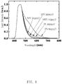
- FIG. 8 illustrates the light intensity of the first experimental example, the second experimental example, the third experimental, the first comparative example, and the second comparative example across the wavelength range from 350 nm to 800 nm according to the second embodiment of the present invention.
- the organic light-emitting diode Z according to the first embodiment of the present invention is described between with reference to FIG. 1 to FIG. 3 .
- the organic light-emitting diode Z provided by the first embodiment of the present invention includes an anode 1 , a cathode 2 , a luminescent layered structure 3 , a hole transport layer 4 and an electron transport layer 5 .
- the hole transport layer 4 is disposed between the anode 1 and the luminescent layered structure 3
- the electron transport layer 5 is disposed between the cathode 2 and the luminescent layered structure 3 .
- the luminescent layered structure 3 has a luminescent layer 31 , a sensitizer layer 32 , and a guiding material 33 .
- the luminescent layer 31 includes a luminescent-layer ground state, a luminescent-layer singlet state and a luminescent-layer triplet state.
- the luminescent layer 31 is a TTA material layer, that is to say, the luminescent-layer singlet state is two times higher than the luminescent-layer triplet state. More specifically, the luminescent layer 31 is preferably made of an anthracene derivative, a pyrene derivative or a perylene derivative; however, the present invention is not limited thereto.
- the anthracene derivative may be but not limited to 9,10-Di(2-naphthyl)anthracene (ADN), 2-methyl-9,10-D(2-naphthyl)anthracene, 2-tert-butyl-9,10-Di(2-naphthyl)anthracene, or 9,9′-dianthracene.
- ADN 9,10-Di(2-naphthyl)anthracene
- 2-methyl-9,10-D(2-naphthyl)anthracene 2-methyl-9,10-D(2-naphthyl)anthracene
- 2-tert-butyl-9,10-Di(2-naphthyl)anthracene 2-tert-butyl-9,10-Di(2-naphthyl)anthracene
- 9,9′-dianthracene 9,9′-dianthracene.
- the sensitizer layer 32 is disposed between the luminescent layer 31 and the hole transport layer 4 .
- the present invention is not limited thereto.
- the position of the luminescent layer 31 and that of the sensitizer layer 32 are exchangeable. That is to say, in other embodiments, the sensitizer layer 32 can be disposed between the luminescent layer 31 and the electron transport layer 5 .
- the sensitizer layer 32 has a sensitizer-layer triplet state, which is between the luminescent-layer singlet state and the luminescent-layer triplet state.
- the material of the sensitizer layer 32 is preferably (8-hydroxyquinoline) metal complex or 10-hydroxybenzo [h] quinoline-metal complex.
- examples of (8-hydroxyquinoline) metal complex may include but not limited to tris(8-hydroxy)-quinoline-aluminium (Alq 3 ) and gallium 8-hydroxyquinolinat (Gaq3)
- examples of 10-hydroxybenzo [h] quinoline-metal complex may include but not limited to bis(10-hydroxybenzo[h]quinolinato)beryllium.
- the sensitizer layer 32 can transport electron holes and acts as a hole transport layer disposed between the luminescent layer 31 and the anode 1 .
- the sensitizer layer 32 can transport electrons and serve as an electron transport layer disposed between the luminescent layer 31 and the cathode 2 .
- the organic light-emitting diode Z of the present invention further includes a guiding material 33 as a dopant of the sensitizer layer 32 .
- the guiding material 33 has a guiding-material triplet state between the sensitizer-layer singlet state and the sensitizer-layer triplet state.
- the guiding material 33 of the luminescent layered structure 3 can also be an independent material layer disposed adjacent to the sensitizer layer 32 , as shown in FIG. 2 .
- the guiding material 33 can a phosphorescent material or a thermal activated delayed fluorescence material.
- the guiding material 33 can be an iridium complex, e.g.
- the element iridium has the property of allowing energy to be transferred between the triplet state and the singlet state, the energy at the sensitizer-layer singlet state S 2 can be transferred to the guiding material triplet state T 3 , and be further transferred to the sensitizer-layer triplet state T 2 .
- the above-mentioned exemplified materials of the guiding material 33 are merely for exemplary purpose; the present invention is not limited thereto.
- FIG. 3 shows an energy level diagram of the luminescent layered structure 3 of the first experimental example.
- the luminescent-layer singlet state S 1 the luminescent-layer triplet state T 1 and the luminescent-layer ground state G 1 of luminescent layer 31
- the sensitizer-layer singlet state S 2 the sensitizer-layer triplet state T 2
- the sensitizer-layer ground state G 2 of the sensitizer layer 32 the guiding-material singlet state S 3 , the guiding-material triplet state T 3 and the guiding material 33 are shown.
- the triplet state T 2 of the sensitizer layer 32 is between the luminescent-layer singlet state S 1 and the luminescent-layer triplet state T 1
- the guiding-material triplet state T 3 is between the sensitizer-layer singlet state S 2 and the sensitizer-layer triplet state T 2 .
- the material of the luminescent layer 31 of the first experimental example is ADN
- that of the sensitizer layer 32 is Alq 3 , in which the energy level of the luminescent layered structure 3 is shown in Table 1 below.
- the sensitizer layer 32 doped with the guiding material 33 is disposed next to the luminescent layer 31 such that the molecules of the sensitizer layer 32 at the sensitizer-layer singlet state S 2 transfer energy to the molecules of the guiding material 33 at the guiding-material triplet state T 3 , in which the transferred energy is further transferred to the molecules of the sensitizer layer 32 at the sensitizer-layer triplet state T 2 .
- the triplet-triplet energy transfer mechanism (TTET) between the sensitizer layer 32 and the luminescent layer 31 occurs, i.e.
- TTAUC triplet-triplet annihilation upconversion mechanism
- the aforementioned TTAUC mechanism occurs among excited triplet state molecules, wherein one excited triplet state molecule transfer energy to another excited triplet state molecule and returns to the ground state, whereas the excited triplet state molecule that receives energy is raised to the singlet state. Thereafter, molecules of the luminescent layer 31 that are raised to the singlet state return to the luminescent-layer ground state G 1 , thereby emitting light of a first color L 1 .
- molecules of the sensitizer layer 32 at the sensitizer-layer singlet state S 2 emits light of a second color L 2 when returning to the sensitizer-layer ground state G 2 .
- white light can be generated by mixing the first color light L 1 , the second color light L 2 , light of a third color.
- ADN as the luminescent layer 31 and with an added light-emitting material that emits red light
- a white light can be obtained by mixing the blue light emitted by AND, the green light emitted by Alq 3 and the red light.
- the present invention is not limited thereto.
- the material of the luminescent layer 31 and that of the sensitizer layer 32 are selected based on a predetermined color of light emitted by the organic light-emitting diode Z, thereby generating light of the predetermined color by mixing the first color light L 1 and the second color light L 2 .
- the present invention enables the energy at the sensitizer-layer singlet state S 2 to participate in the light-emitting mechanism of the organic light-emitting diode Z with the guiding material 33 , thereby increasing the efficiency of the organic light-emitting diode Z.
- the material of the sensitizer layer 32 of the present experimental example is Alq 3 that emits green light, and that of the luminescent layer 31 is ADN, which emits blue light; therefore, in order to prevent the green second color light L 2 emitted when molecules at the sensitizer-layer singlet state S 2 return to ground state from affecting the blue first color light L 1 , the present embodiment enables at least part of the energy at the sensitizer-layer singlet state S 2 to be transferred to the sensitizer-layer triplet state T 2 through the luminescent layer 31 such that the color purity of the first color light L 1 is enhanced.
- the present invention is not limited to the above description.
- the predetermined emission color of the organic light-emitting diode Z is not the first color light L 1
- a person skilled in the art can select the material of the sensitizer layer and that of the luminescent layer according to actual needs.
- the material of the sensitizer layer 32 can be decided based on the predetermined light color of the organic light-emitting diode Z.
- the predetermined light color is white
- a material that has a singlet state lower than the luminescent-layer singlet state S 1 can be chosen as the material of the sensitizer layer 32 , as in the case of the first experimental example, so that the second color light L 2 is green.
- the organic light-emitting diode Z can emit white light.
- the predetermined light color of the organic light-emitting diode Z is blue
- a material that has a singlet state higher than the luminescent-layer singlet state S 1 can be chosen to be the material of the sensitizer layer 32 , as in the case of the second experimental example, so that the second color light L 2 and the first light color L 1 are both blue light.
- the first embodiment of the present invention uses mainly the triplet energy thereof to emit light through the technical solution of the sensitizer layer 32 doped with the guiding material 33 , which serves as the place the recombination between the positive polarons and the negative polarons takes place such that triplet-triplet annihilation upconversion mechanism can be triggered in the luminescent layer 31 by the triplet excitons in the sensitizer layer 32 that are generated from the recombination. Since the sensitizer layer 32 acts as the recombination zone in the present embodiment, high energy polarons in the luminescent layer 31 are prevented from reacting with the excitons.
- the triplet energy in the sensitizer layer 32 can be utilized by being transferred and converted to emit light, thereby enhancing the illumination efficiency of the organic light-emitting diode Z and extending the lifetime thereof.
- the guiding-material triplet state T 3 of the guiding material 33 is between the sensitizer-layer singlet state S 2 and the sensitizer-layer triplet state T 2 , thereby enabling the energy at the sensitizer-layer singlet state S 2 to be transferred to the guiding-material triplet state T 3 of the guiding material 33 , and then to the sensitizer-layer triplet state T 2 of the sensitizer layer 32 .
- the efficiency of the organic light-emitting diode Z can be enhanced.
- the color purity of the first color light L 1 can be increased.
- the main difference between the present embodiment and the first embodiment lies in that the organic light-emitting diode Z of the second embodiment further includes a blocking layer 34 between the luminescent layer 31 and the guiding-material-doped sensitizer layer 32 .
- the blocking layer 34 has a blocking-layer singlet state S 4 and a blocking-layer triplet state T 4 , in which the blocking-layer singlet state S 4 is higher than the luminescent-layer singlet state S 1 , and the blocking-layer triplet state T 4 is higher than the luminescent-layer triplet state T 1 .
- the triplet energy of the sensitizer layer 32 can be transferred to the triplet state of the luminescent layer 31 .
- the quenching effects between the sensitizer layer 32 and the luminescent layer 31 can be reduced. In this way, the illumination efficiency of the organic light-emitting diode Z can be further improved.
- the material of the guiding material 33 can be 1-(2′5-dimethyl-4-(1-pyrenyl)phenyl)pyrene (DMPPP) or 1,3,5-Tri(1-pyrenyl)benzene (TPB3).
- DMPPP 1-(2′5-dimethyl-4-(1-pyrenyl)phenyl)pyrene
- TPB3 1,3,5-Tri(1-pyrenyl)benzene
- the present invention is not limited thereto.
- the guiding material 33 of the present experimental example is DMPPP
- the materials of the luminescent layer 31 , the sensitizer layer 32 , and the guiding material 33 are ADN, Alq 3 , and Ir(ppy)3 respectively.
- the energy level of FIG. 5 is shown in Table 2 below.
- FIG. 6 shows the transient electroluminescence of the organic light-emitting diode Z of the first experimental example according to the present embodiment.
- ITO indium tin oxide
- LiF/Al is used as the cathode 2 .
- the thickness of the hole transport layer 4 is 50 nm, and the material thereof is N,N′-di(1-naphthyl)-N,N′-diphenyl benzidine (NPB).
- the thickness of the electron transport layer 5 is 65 nm, and the material thereof is 4,7-diphenyl-1,10-phenanthroline (Bphen).
- the thickness of the sensitizer layer 32 is 5 nm, and the material thereof is Alq 3 .
- the sensitizer layer 32 is doped with 3% of the guiding material 33 .
- the thickness of the luminescent layer 31 is 10 nm, and the material thereof is ADN. It should be noted that the above description regarding the materials used and the specifications thereof are the exemplary embodiment of the present invention; the present invention is not limited thereto.
- the transient electroluminescence of the organic light-emitting diode Z is measured by first applying an electro-pulse to the organic light-emitting diode Z, and the light emitted by the organic light-emitting diode Z in response to the electro-pulse is gauged and converted into electric output with a photomultiplier.
- the curves shown in FIG. 6 respectively represent the electric signals outputted by the organic light-emitting diode Z in response to an input voltage of 3.8 V, 4.2 V, 4.6 V, 5.0 V, 5.4 V, 5.8 V, and 6 V-6.2 V. As shown in FIG.
- the speed at which the organic light-emitting diode Z of the first experimental example emits light is of microsecond-scale.
- the speed at which singlet excitons emit light is of nanosecond-scale, and that of triplet excitons is of microsecond-scale since triplet excitons decay slower owing to the spin conservation. This is due to the delay rate of triplet excitons being slower. That is to say, FIG. 6 shows that in the first experimental example the triplet excitons contribute to nearly 100% of the total emission.
- FIG. 7 shows a diagram illustrating the external quantum efficiency of the first experimental example (the sensitizer layer 32 doped with 3% of the guiding material 33 , shown with the curve marked as 3% Ir(ppy)3), the second experimental example (the sensitizer layer 32 doped with 10% of the guiding material 33 , shown with the curve marked as 10% Ir(ppy)3), the third experimental example (the sensitizer layer 32 doped with 50% of the guiding material 33 , shown with the curve marked as 50% Ir(ppy)3), a first comparative example (the sensitizer layer 32 without dopant, shown with the curve marked as 0% Ir(ppy)3), and a second comparative example (the sensitizer layer 32 is replaced by the guiding material 33 , shown with the curve marked as 100% Ir(ppy)3) according to the second embodiment of the present invention.
- the result is due to the effect that the energy at the sensitizer-layer singlet state S 2 of the sensitizer layer 32 is transferred to the sensitizer-layer triplet state T 2 of the sensitizer layer 32 through the guiding material 33 , and then participates in the light-emitting mechanism through the triplet triplet energy transfer (TTET) and the triplet-triplet annihilation upconversion (TTAUC) together with the molecules of the sensitizer layer 32 at the sensitizer-layer triplet state T 2 in the first place.
- TTET triplet triplet energy transfer
- TTAUC triplet-triplet annihilation upconversion
- FIG. 8 shows a light intensity diagram of the first experimental example to the third experimental example, the first comparative example and the second comparative example across a range of wavelength.
- the first comparative example which contains no guiding material 33 as a dopant has higher light intensity at the wavelength range of 495 ⁇ 570 nm compared to the first experimental example, the second experimental example, the third experimental, and the second comparative example in which the sensitizer layer 32 is doped with the guiding material 33 .
- the guiding material 33 as a dopant guides the energy at the sensitizer-layer singlet state S 2 to the sensitizer-layer triplet state T 2 .
- the higher the dopant concentration of the guiding material 33 the higher the color purity of the first color light L 1 , which is blue light emitted by ADN.
- the guiding material 33 replaces the sensitizer layer 32 , which is the case of the second comparative example
- the color purity of the second comparative example is still higher than that of the first comparative example, which is mainly because the element iridium in Ir(ppy)3 allows energy to be transferred from the singlet state to the triplet state and vice versa.
- the energy of the guiding-material singlet state S 3 can be transferred to the guiding-material triplet state T 3 , and further participates in the light-emitting mechanism through taking part in the triplet-triplet energy transfer (TTET).
- TTET triplet-triplet energy transfer
- the embodiments of the present invention achieves “the molecules of the sensitizer layer at the sensitizer-layer singlet state transfer energy to the molecules of the guiding material at the guiding-material triplet state, in which the transferred energy is further transferred to the molecules of the sensitizer layer at the sensitizer-layer triplet state” through the technical solutions of “the luminescent layered structure includes the guiding material” and “the guiding-material triplet state is between the sensitizer-layer singlet state and the sensitizer-layer triplet state”.
- the organic light-emitting diode Z of the present embodiments utilizes the guiding-material triplet state T 3 of the guiding material 33 to transfer energy from the sensitizer-layer singlet state S 2 to the sensitizer-layer triplet state T 2 so that the energy at the sensitizer-layer singlet state S 2 can contribute to light emission, thereby enhancing the efficiency of the organic light-emitting diode Z and increasing the color purity of the first color light L 1 .
- the sensitizer layer 32 performs triplet-triplet energy transfer with the luminescent layer 31 , thereby triggering triplet-triplet annihilation upconversion mechanism in the luminescent layer 31 .
- triplet energy of the luminescent layer 31 and that of the sensitizer layer 32 can be converted into light emitted by the organic light-emitting diode Z, thereby effectively enhancing the illumination efficiency and lifespan of the organic light-emitting diode Z.
- a blocking layer 34 can be added in the organic light-emitting diode Z, in which the singlet state of the blocking layer 34 is higher than that of the luminescent layer 31 , and the triplet state of the blocking layer 34 is higher than that of the luminescent layer 31 . In this way, the illumination efficiency of the organic light-emitting diode Z can be further increased.
Landscapes
- Physics & Mathematics (AREA)
- Optics & Photonics (AREA)
- Chemical & Material Sciences (AREA)
- Engineering & Computer Science (AREA)
- Materials Engineering (AREA)
- Inorganic Chemistry (AREA)
- Spectroscopy & Molecular Physics (AREA)
- Electroluminescent Light Sources (AREA)
Abstract
Description
| TABLE 1 | |||||
| Sensitizer | | Luminescent | |||
| layer | |||||
| 32 | |
|
|||
| Singlet state (eV) | 2.8 | 2.9 | 2.83 | ||
| Triplet state (eV) | 2.0 | 2.4 | 1.67 | ||
| TABLE 2 | ||||
| Sensitizer | Guiding | Blocking | | |
| layer | ||||
| 32 | |
|
|
|
| Singlet state (eV) | 2.8 | 2.9 | 3.15 | 2.83 |
| Triplet state (eV) | 2.0 | 2.4 | 2.05 | 1.67 |
Claims (17)
Priority Applications (1)
| Application Number | Priority Date | Filing Date | Title |
|---|---|---|---|
| US16/354,826 US10784458B1 (en) | 2019-03-15 | 2019-03-15 | Organic light-emitting diode with enhanced light-emitting efficiency and color purity |
Applications Claiming Priority (1)
| Application Number | Priority Date | Filing Date | Title |
|---|---|---|---|
| US16/354,826 US10784458B1 (en) | 2019-03-15 | 2019-03-15 | Organic light-emitting diode with enhanced light-emitting efficiency and color purity |
Publications (2)
| Publication Number | Publication Date |
|---|---|
| US20200295289A1 US20200295289A1 (en) | 2020-09-17 |
| US10784458B1 true US10784458B1 (en) | 2020-09-22 |
Family
ID=72424162
Family Applications (1)
| Application Number | Title | Priority Date | Filing Date |
|---|---|---|---|
| US16/354,826 Active US10784458B1 (en) | 2019-03-15 | 2019-03-15 | Organic light-emitting diode with enhanced light-emitting efficiency and color purity |
Country Status (1)
| Country | Link |
|---|---|
| US (1) | US10784458B1 (en) |
Families Citing this family (2)
| Publication number | Priority date | Publication date | Assignee | Title |
|---|---|---|---|---|
| US20200373360A1 (en) * | 2019-05-23 | 2020-11-26 | Universal Display Corporation | Oled display panel with unpatterned emissive stack |
| CN113471376B (en) * | 2021-06-28 | 2024-03-19 | 广东聚华印刷显示技术有限公司 | Light emitting structure, organic light emitting diode and electronic device |
Citations (8)
| Publication number | Priority date | Publication date | Assignee | Title |
|---|---|---|---|---|
| US20020146589A1 (en) * | 2000-05-22 | 2002-10-10 | Kimio Akiyama | Organic electroluminescent device and light-emitting material |
| US20090200925A1 (en) * | 2006-06-13 | 2009-08-13 | Konica Minolta Holdings, Inc. | Organic electroluminescent element, lighting device and display device |
| US20110049367A1 (en) * | 2008-03-19 | 2011-03-03 | Stephen Forrest | Organic thin films for infrared detection |
| US20140077172A1 (en) * | 2012-09-07 | 2014-03-20 | Universal Display Corporation | Phosphorescence-sensitized delayed fluorescence light emitting system |
| US20150076360A1 (en) * | 2013-09-16 | 2015-03-19 | Saint-Gobain Ceramics & Plastics, Inc. | Scintillator and radiation detector including the scintillator |
| US20160197282A1 (en) * | 2013-08-16 | 2016-07-07 | Konica Minolta, Inc. | Organic electroluminescent element, light emitting device, lighting device, display device and electronic device |
| US20180051204A1 (en) * | 2015-02-06 | 2018-02-22 | Idemitsu Kosan Co., Ltd. | Organic electroluminescence element and electronic device |
| US20180212157A1 (en) * | 2014-07-31 | 2018-07-26 | Tomohiro Oshiyama | Organic electroluminescent device, thin luminous film, display apparatus, and lighting apparatus |
-
2019
- 2019-03-15 US US16/354,826 patent/US10784458B1/en active Active
Patent Citations (8)
| Publication number | Priority date | Publication date | Assignee | Title |
|---|---|---|---|---|
| US20020146589A1 (en) * | 2000-05-22 | 2002-10-10 | Kimio Akiyama | Organic electroluminescent device and light-emitting material |
| US20090200925A1 (en) * | 2006-06-13 | 2009-08-13 | Konica Minolta Holdings, Inc. | Organic electroluminescent element, lighting device and display device |
| US20110049367A1 (en) * | 2008-03-19 | 2011-03-03 | Stephen Forrest | Organic thin films for infrared detection |
| US20140077172A1 (en) * | 2012-09-07 | 2014-03-20 | Universal Display Corporation | Phosphorescence-sensitized delayed fluorescence light emitting system |
| US20160197282A1 (en) * | 2013-08-16 | 2016-07-07 | Konica Minolta, Inc. | Organic electroluminescent element, light emitting device, lighting device, display device and electronic device |
| US20150076360A1 (en) * | 2013-09-16 | 2015-03-19 | Saint-Gobain Ceramics & Plastics, Inc. | Scintillator and radiation detector including the scintillator |
| US20180212157A1 (en) * | 2014-07-31 | 2018-07-26 | Tomohiro Oshiyama | Organic electroluminescent device, thin luminous film, display apparatus, and lighting apparatus |
| US20180051204A1 (en) * | 2015-02-06 | 2018-02-22 | Idemitsu Kosan Co., Ltd. | Organic electroluminescence element and electronic device |
Also Published As
| Publication number | Publication date |
|---|---|
| US20200295289A1 (en) | 2020-09-17 |
Similar Documents
| Publication | Publication Date | Title |
|---|---|---|
| KR101614403B1 (en) | White oled with blue light-emitting layers | |
| JP4241612B2 (en) | Phosphorescent light emitting device having organic layer | |
| US8441004B2 (en) | Radiation emitting device and method for the production thereof | |
| US10319931B2 (en) | Light emitting device, method for manufacturing light emitting device, and display device | |
| US20060066231A1 (en) | Electroluminescence element | |
| US20090001875A1 (en) | Organic light-emitting device incorporating multifunctional osmium complexes | |
| CN104253146A (en) | Organic light emitting diode array substrate and display device | |
| CN104167428A (en) | Organic light emitting diode array substrate and display device | |
| KR101941084B1 (en) | Organic Light Emitting Diode Device | |
| KR20110082557A (en) | Radiation emitter | |
| KR102574241B1 (en) | Organic Light Emitting Device and Organic Light Emitting Display Device Using the Same | |
| JP5576122B2 (en) | Organic light-emitting diodes with a barrier layer made of ambipolar materials | |
| US10784458B1 (en) | Organic light-emitting diode with enhanced light-emitting efficiency and color purity | |
| US10700303B1 (en) | Organic light-emitting diode | |
| KR20160054820A (en) | Blue phosphorescent organic light emitting diode device having improved efficiency by suppressing triplet exciton quenching and acheiving charge balance | |
| KR101536568B1 (en) | Blue phosphorescent organic light emitting diode device having improved efficiency by suppressing triplet exciton quenching | |
| KR101536569B1 (en) | Blue phosphorescent organic light emitting diode device having improved efficiency by controlling recombination zone spatially | |
| TWI699919B (en) | Organic light-emitting diode | |
| JP2014182933A (en) | Organic el light-emitting apparatus | |
| KR102536929B1 (en) | Organic light emitting diode | |
| JP2006108190A (en) | Electroluminescence element | |
| US8735879B2 (en) | Organic light-emitting diode comprising at least two electroluminescent layers | |
| KR20070027796A (en) | Organic EL device having a plurality of light emitting layers | |
| CN117693211B (en) | Organic electroluminescent diode and manufacturing method thereof | |
| KR101857293B1 (en) | Organic light emitting diode |
Legal Events
| Date | Code | Title | Description |
|---|---|---|---|
| FEPP | Fee payment procedure |
Free format text: ENTITY STATUS SET TO UNDISCOUNTED (ORIGINAL EVENT CODE: BIG.); ENTITY STATUS OF PATENT OWNER: LARGE ENTITY |
|
| AS | Assignment |
Owner name: SHINE MATERIALS TECHNOLOGY CO., LTD., TAIWAN Free format text: ASSIGNMENT OF ASSIGNORS INTEREST;ASSIGNORS:LEE, JIUN-HAW;CHIU, TIEN-LUNG;CHEN, CHIA-HSUN;AND OTHERS;SIGNING DATES FROM 20190325 TO 20190327;REEL/FRAME:048773/0729 Owner name: TETRAHEDRON TECHNOLOGY CORPORATION, TAIWAN Free format text: ASSIGNMENT OF ASSIGNORS INTEREST;ASSIGNORS:LEE, JIUN-HAW;CHIU, TIEN-LUNG;CHEN, CHIA-HSUN;AND OTHERS;SIGNING DATES FROM 20190325 TO 20190327;REEL/FRAME:048773/0729 Owner name: YUAN ZE UNIVERSITY, TAIWAN Free format text: ASSIGNMENT OF ASSIGNORS INTEREST;ASSIGNORS:LEE, JIUN-HAW;CHIU, TIEN-LUNG;CHEN, CHIA-HSUN;AND OTHERS;SIGNING DATES FROM 20190325 TO 20190327;REEL/FRAME:048773/0729 Owner name: WISECHIP SEMICONDUCTOR INC., TAIWAN Free format text: ASSIGNMENT OF ASSIGNORS INTEREST;ASSIGNORS:LEE, JIUN-HAW;CHIU, TIEN-LUNG;CHEN, CHIA-HSUN;AND OTHERS;SIGNING DATES FROM 20190325 TO 20190327;REEL/FRAME:048773/0729 Owner name: NICHEM FINE TECHNOLOGY CO, LTD., TAIWAN Free format text: ASSIGNMENT OF ASSIGNORS INTEREST;ASSIGNORS:LEE, JIUN-HAW;CHIU, TIEN-LUNG;CHEN, CHIA-HSUN;AND OTHERS;SIGNING DATES FROM 20190325 TO 20190327;REEL/FRAME:048773/0729 |
|
| STCF | Information on status: patent grant |
Free format text: PATENTED CASE |
|
| MAFP | Maintenance fee payment |
Free format text: PAYMENT OF MAINTENANCE FEE, 4TH YEAR, LARGE ENTITY (ORIGINAL EVENT CODE: M1551); ENTITY STATUS OF PATENT OWNER: LARGE ENTITY Year of fee payment: 4 |