US10771230B2 - Estimating apparatus for bias drift of transmitting end modulator, compensating apparatus and receiver - Google Patents
Estimating apparatus for bias drift of transmitting end modulator, compensating apparatus and receiver Download PDFInfo
- Publication number
- US10771230B2 US10771230B2 US15/291,141 US201615291141A US10771230B2 US 10771230 B2 US10771230 B2 US 10771230B2 US 201615291141 A US201615291141 A US 201615291141A US 10771230 B2 US10771230 B2 US 10771230B2
- Authority
- US
- United States
- Prior art keywords
- transmitting end
- received signals
- bias drift
- modulator
- end modulator
- Prior art date
- Legal status (The legal status is an assumption and is not a legal conclusion. Google has not performed a legal analysis and makes no representation as to the accuracy of the status listed.)
- Expired - Fee Related, expires
Links
Images


Classifications
-
- H—ELECTRICITY
- H04—ELECTRIC COMMUNICATION TECHNIQUE
- H04L—TRANSMISSION OF DIGITAL INFORMATION, e.g. TELEGRAPHIC COMMUNICATION
- H04L7/00—Arrangements for synchronising receiver with transmitter
- H04L7/0075—Arrangements for synchronising receiver with transmitter with photonic or optical means
-
- H—ELECTRICITY
- H04—ELECTRIC COMMUNICATION TECHNIQUE
- H04L—TRANSMISSION OF DIGITAL INFORMATION, e.g. TELEGRAPHIC COMMUNICATION
- H04L27/00—Modulated-carrier systems
- H04L27/0014—Carrier regulation
-
- H—ELECTRICITY
- H04—ELECTRIC COMMUNICATION TECHNIQUE
- H04L—TRANSMISSION OF DIGITAL INFORMATION, e.g. TELEGRAPHIC COMMUNICATION
- H04L27/00—Modulated-carrier systems
- H04L27/26—Systems using multi-frequency codes
-
- H—ELECTRICITY
- H04—ELECTRIC COMMUNICATION TECHNIQUE
- H04L—TRANSMISSION OF DIGITAL INFORMATION, e.g. TELEGRAPHIC COMMUNICATION
- H04L27/00—Modulated-carrier systems
- H04L27/0014—Carrier regulation
- H04L2027/0024—Carrier regulation at the receiver end
-
- H—ELECTRICITY
- H04—ELECTRIC COMMUNICATION TECHNIQUE
- H04L—TRANSMISSION OF DIGITAL INFORMATION, e.g. TELEGRAPHIC COMMUNICATION
- H04L27/00—Modulated-carrier systems
- H04L27/0014—Carrier regulation
- H04L2027/0024—Carrier regulation at the receiver end
- H04L2027/0026—Correction of carrier offset
- H04L2027/0038—Correction of carrier offset using an equaliser
-
- H—ELECTRICITY
- H04—ELECTRIC COMMUNICATION TECHNIQUE
- H04L—TRANSMISSION OF DIGITAL INFORMATION, e.g. TELEGRAPHIC COMMUNICATION
- H04L27/00—Modulated-carrier systems
- H04L27/0014—Carrier regulation
- H04L2027/0083—Signalling arrangements
- H04L2027/0085—Signalling arrangements with no special signals for synchronisation
-
- H—ELECTRICITY
- H04—ELECTRIC COMMUNICATION TECHNIQUE
- H04L—TRANSMISSION OF DIGITAL INFORMATION, e.g. TELEGRAPHIC COMMUNICATION
- H04L27/00—Modulated-carrier systems
- H04L27/32—Carrier systems characterised by combinations of two or more of the types covered by groups H04L27/02, H04L27/10, H04L27/18 or H04L27/26
- H04L27/34—Amplitude- and phase-modulated carrier systems, e.g. quadrature-amplitude modulated carrier systems
- H04L27/38—Demodulator circuits; Receiver circuits
- H04L27/3818—Demodulator circuits; Receiver circuits using coherent demodulation, i.e. using one or more nominally phase synchronous carriers
- H04L27/3827—Demodulator circuits; Receiver circuits using coherent demodulation, i.e. using one or more nominally phase synchronous carriers in which the carrier is recovered using only the demodulated baseband signals
Definitions
- the present disclosure relates to the field of communications, and in particular to an estimating apparatus for bias drift of a transmitting end modulator, a compensating apparatus and a receiver, and a method.
- the vector modulator may move spectra of an electrical domain to near optical frequencies with almost no loss, to achieve a high spectral utilization in combination with a coherent monitor technology at a receiver end.
- a bias voltage of the modulator needs to be accurately set.
- bias drift occurs.
- modulation signals such as quadrature phase shift keying (QPSK) or quadrature amplitude modulation (QAM)
- QPSK quadrature phase shift keying
- QAM quadrature amplitude modulation
- Embodiments of the present disclosure provide an estimating apparatus for bias drift of a transmitting end modulator, a compensating apparatus and a receiver, and a method, in which estimation and compensation of the bias drift are performed directly at the receiving end according to phase recovered received signals, with no need of providing an extra bias control circuit at the transmitting end, which makes the system simple in structure, and is applicable to various modulation formats, with a wide range of applicability, and may meet demands of high-order modulation formats; and furthermore, it may be used simultaneously with a bias control circuit of an existing transmitter, thereby further improving precision of estimation and compensation of the bias drift.
- an estimating apparatus for bias drift of a transmitting end modulator including: a recovering unit configured to perform phase recovery on received signals, to remove a frequency difference and a phase difference between a transmitting end laser and a receiving end laser; and an estimating unit configured to estimate the bias drift of the transmitting end modulator according to phase recovered received signals.
- a compensating apparatus for bias drift of a transmitting end modulator including: the estimating apparatus as described in the first aspect of the present disclosure; and a third compensating unit configured to compensate for the bias drift of the transmitting end modulator according to estimated bias drift of the transmitting end modulator.
- a receiver including the estimating apparatus as described in the first aspect of the present disclosure or the compensating apparatus as described in the second aspect of the present disclosure.
- An advantage of the embodiments of the present disclosure exists in that estimation and compensation of the bias drift are performed directly at the receiving end according to phase recovered received signals, with no need of providing an extra bias control circuit at the transmitting end, which makes the system simple in structure, and is applicable to various modulation formats, with a wide range of applicability, and may meet demands of high-order modulation formats; and furthermore, it may be used simultaneously with a bias control circuit of an existing transmitter, thereby further improving precision of estimation and compensation of the bias drift.
- FIG. 1 is a schematic diagram of a structure of the estimating apparatus for bias drift of a transmitting end modulator of Embodiment 1 of the present disclosure
- FIG. 2 is a schematic diagram of a structure of the transmitting end modulator of Embodiment 1 of the present disclosure
- FIG. 3 is a schematic diagram of a structure of the recovering unit of Embodiment 1 of the present disclosure
- FIG. 4 is a schematic diagram of a structure of the compensating apparatus for bias drift of a transmitting end modulator of Embodiment 2 of the present disclosure
- FIG. 5 is a schematic diagram of a structure of the third compensating unit of Embodiment 2 of the present disclosure.
- FIG. 6 is a schematic diagram of the controlling of a controlling unit of Embodiment 2 of the present disclosure.
- FIG. 7 is another schematic diagram of the structure of the third compensating unit of Embodiment 2 of the present disclosure.
- FIG. 8 is a further schematic diagram of a structure of the third compensating unit of Embodiment 2 of the present disclosure.
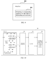
- FIG. 9 is a schematic diagram of a structure of the receiver of Embodiment 3 of the present disclosure.
- FIG. 10 is a block diagram of a systematic structure of the receiver of Embodiment 3 of the present disclosure.
- FIG. 11 is a flowchart of the estimating method for bias drift of a transmitting end modulator of Embodiment 4 of the present disclosure.
- FIG. 12 is a flowchart of the compensating method for bias drift of a transmitting end modulator of Embodiment 5 of the present disclosure.
- FIG. 1 is a schematic diagram of a structure of the estimating apparatus for bias drift of a transmitting end modulator of Embodiment 1 of the present disclosure.
- the apparatus 100 includes:
- estimation and compensation of the bias drift are performed directly at the receiving end according to phase recovered received signals, with no need of providing an extra bias control circuit at the transmitting end, which makes the system simple in structure, and is applicable to various modulation formats, with a wide range of applicability, and may meet demands of high-order modulation formats; and furthermore, it may be used simultaneously with a bias control circuit of an existing transmitter, thereby further improving precision of estimation and compensation of the bias drift.
- the received signals refer to signals in an optical communications system transmitted from a transmitting end and received in a receiving end after passing a transmission link.
- FIG. 2 is a schematic diagram of a structure of the transmitting end modulator of Embodiment 1 of the present disclosure.
- a transmission signal A(t) is formed from light emitted from a laser 201 and modulated by a vector modulator 202 , the vector modulator 202 being provided with three bias points, a real part bias point Bias I, an imaginary part bias point Bias Q, and a phase bias point Bias Phase; and furthermore, radio frequency input RF is further provided.
- a direct current signal is generated in a real part or an imaginary part of the transmission signal, which results in an imbalance of amplitudes of the real part signal and the imaginary part signal, and further result in an extra phase difference between the real part signal and the imaginary part signal.
- the transmission signal modulated by the vector modulator where bias drift occurs may be expressed by Formula (1) below:
- A(t) denotes a transmission signal
- t denotes a time
- k I and k Q respectively denote amplitudes of a real part signal and an imaginary part signal
- I(t) and Q(t) respectively denote the real part signal and the imaginary part signal
- I 0 and Q 0 respectively denote a direct current signal generated in the real part signal and the imaginary part signal
- e denotes a phase difference between the real part signal and the imaginary part signal.
- the bias drift of the vector modulator may include the imbalance k I /k Q of the amplitudes of the real part signal and the imaginary part signal, the direct current signal I 0 generated in the real part signal, the direct current signal Q 0 generated in the imaginary part signal, and the phase difference ⁇ between the real part signal and the imaginary part signal.
- the recovering unit 101 performs phase recovery on the received signals, to remove the frequency difference and the phase difference between the transmitting end laser and the receiving end laser.
- the above Formula (1) which expresses the transmission signal may be used to express the phase recovered received signals, that is, the received signals with the frequency difference and the phase difference between the transmitting end laser and the receiving end laser being removed.
- a structure of the recovering unit 101 and a method of phase recovery of this embodiment shall be illustrated below.
- FIG. 3 is a schematic diagram of the structure of the recovering unit 101 of Embodiment 1 of the present disclosure. As shown in FIG. 3 , the recovering unit 101 includes:
- phase recovery of this embodiment is illustrated above. However, this embodiment is not limited thereto, and all phase recovery methods are applicable to this embodiment when they are able to remove the frequency difference and the phase difference between the transmitting end laser and the receiving end laser.
- the estimating unit 102 estimates the bias drift of the transmitting end modulator according to the phase recovered received signals.
- the phase recovered received signals that may be expressed by above Formula (1)
- the following bias drift may be estimated by using an existing method: the imbalance kI/kQ of the amplitudes of the real part signal and the imaginary part signal, the direct current signal I 0 generated in the real part signal, the direct current signal Q 0 generated in the imaginary part signal, and the phase difference ⁇ between the real part signal and the imaginary part signal.
- kI/kQ, I 0 , Q 0 and ⁇ may be calculated according to the following existing method: a) respectively calculating average values of the real part and the imaginary part of the received signal, and taking them respectively as I 0 and Q 0 ; b) calculating a power ratio of the real part and the imaginary part, and obtaining kI/kQ by calculating a root of the power ratio; and c) calculating an average value of the real part multiplied by the imaginary part and an average value of squares of the imaginary part, and obtaining ⁇ tan( ⁇ ) by dividing the former by the latter, hence obtaining the phase difference ⁇ .
- the estimating apparatus 100 for bias drift of a transmitting end modulator may further include:
- the estimating apparatus 100 for bias drift of a transmitting end modulator may further include:
- the estimating apparatus 100 for bias drift of a transmitting end modulator may further include:
- the demultiplexing unit 105 may be used to demultiplex the received signals, to obtain the received signals in the two polarization states.
- the pilot signals interpolated into the transmission signals may be used to perform the demultiplexing
- a training sequence at the transmitting end may be used to perform the demultiplexing
- a decision-based adaptive method may be used to perform the demultiplexing.
- the first compensating unit 103 , the second compensating unit 104 and the demultiplexing unit 105 are optional, and are shown by dashed boxes in FIG. 1 .
- estimation and compensation of the bias drift are performed directly at the receiving end according to phase recovered received signals, with no need of providing an extra bias control circuit at the transmitting end, which makes the system simple in structure, and is applicable to various modulation formats, with a wide range of applicability, and may meet demands of high-order modulation formats; and furthermore, it may be used simultaneously with a bias control circuit of an existing transmitter, thereby further improving precision of estimation and compensation of the bias drift.
- FIG. 4 is a schematic diagram of a structure of the compensating apparatus for bias drift of a transmitting end modulator of Embodiment 2 of the present disclosure.
- the apparatus 400 includes:
- a structure and functions of the estimating apparatus 401 for bias drift of a transmitting end modulator are identical to those described in Embodiment 1, and shall not be described herein any further.
- a structure of the third compensating unit 402 and a method for compensating for the bias drift of the transmitting end modulator of this embodiment shall be illustrated below.
- FIG. 5 is a schematic diagram of a structure of the third compensating unit of Embodiment 2 of the present disclosure.
- the third compensating unit 402 includes:
- the third compensating unit 402 when the third compensating unit 402 includes the controlling unit 501 , the third compensating unit 402 may be arranged at the transmitting end.
- the controlling unit 501 controls the bias points of the transmitting end modulator according to the estimated bias drift.
- FIG. 6 is a schematic diagram of the controlling of a controlling unit of Embodiment 2 of the present disclosure, as shown in FIG. 6 , the controlling unit 501 is arranged in the transmitting end, the estimated bias drift estimated in the receiving end is feedback to the controlling unit 501 to be taken as a reference value for controlling the bias points, and the bias points are adjusted, so that the re-estimated bias drift gradually becomes small starting from the reference value.
- FIG. 7 is another schematic diagram of the structure of the third compensating unit 402 of Embodiment 2 of the present disclosure. As shown in FIG. 7 , the third compensating unit 402 includes:
- the fourth compensating unit 601 compensates for the received signals according to the estimated bias drift, such as subtracting an amount of the estimated bias drift from the received signals.
- the first equalizing unit 602 may perform equalization processing on the compensated received signals by using an existing method.
- an existing method For example, a blind equalization algorithm, a decision-based adaptive method and a training sequence-based equalization method, etc., may be used.
- FIG. 8 is a further schematic diagram of the structure of the third compensating unit 402 of Embodiment 2 of the present disclosure. As shown in FIG. 8 , the third compensating unit 402 includes:
- the equalization processing needs to be performed according to a reference signal, and the modifying unit 701 is configured to modify the reference signal according to the estimated bias drift.
- the reference signal may be modified according to above Formula (1).
- the second equalizing unit 702 performs equalization processing on the received signals according to the modified reference signal.
- estimation and compensation of the bias drift are performed directly at the receiving end according to phase recovered received signals, with no need of providing an extra bias control circuit at the transmitting end, which makes the system simple in structure, and is applicable to various modulation formats, with a wide range of applicability, and may meet demands of high-order modulation formats; and furthermore, it may be used simultaneously with a bias control circuit of an existing transmitter, thereby further improving precision of estimation and compensation of the bias drift.
- FIG. 9 is a schematic diagram of a structure of the receiver of Embodiment 3 of the present disclosure.
- the receiver 800 includes an estimating or compensating apparatus 801 for bias drift of a transmitting end modulator, a structure and functions of the estimating or compensating apparatus 801 being identical to those contained in Embodiment 1 or 2, and being not going to be described herein any further.
- FIG. 10 is a block diagram of a systematic structure of the receiver of Embodiment 3 of the present disclosure.
- the receiver 900 includes: a front end configured to convert inputted optical signals into baseband signals in two polarization states.
- the two polarization states may include an H polarization state and a V polarization state.
- the front end includes: a local oscillator laser 910 , an optical 90 deg hybrid 901 , optoelectronic (O/E) detectors 902 , 904 , 906 and 908 , analog-to-digital converters (ADCs) 903 , 905 , 907 and 909 , a dispersion compensator 911 , an equalizer 912 and an estimating or compensating apparatus 913 for bias drift of a transmitting end modulator.
- O/E optoelectronic
- ADCs analog-to-digital converters
- a structure and functions of the estimating or compensating apparatus 913 are identical to those described in Embodiment 1 or 2, and shall not be described herein any further;
- the local oscillator laser 910 is configured to provide a local light source, and optical signals are converted into baseband signals in one polarization state after passing through the optical 90 deg hybrid 901 , the optoelectronic (O/E) detectors 902 and 904 and the analog-to-digital converters (ADCs) 903 and 905 , and are converted into baseband signals in the other polarization state after passing through the optical 90 deg hybrid 901 , the optoelectronic (O/E) detectors 906 and 908 and the analog-to-digital converters (ADCs) 907 and 909 ; and a particular process of implementation is similar to that in the related art, and shall not be described herein any further.
- estimation and compensation of the bias drift are performed directly at the receiving end according to phase recovered received signals, with no need of providing an extra bias control circuit at the transmitting end, which makes the system simple in structure, and is applicable to various modulation formats, with a wide range of applicability, and may meet demands of high-order modulation formats; and furthermore, it may be used simultaneously with a bias control circuit of an existing transmitter, thereby further improving precision of estimation and compensation of the bias drift.
- An embodiment of the present disclosure further provides an estimating method for bias drift of a transmitting end modulator, corresponding to the estimating apparatus for bias drift of a transmitting end modulator of Embodiment 1.
- FIG. 11 is a flowchart of the estimating method for bias drift of a transmitting end modulator of Embodiment 4 of the present disclosure. As shown in FIG. 11 , the method includes:
- Steps 1001 , 1003 and 1004 are optional. And when Steps 1001 , 1003 and 1004 are not included, phase recovery is performed directly on the received signals in Step 1002 , and the bias drift of the transmitting end modulator are directly estimated according to phase recovered received signals in Step 1005 .
- a method for compensating for an imbalance between a real part and an imaginary part generated by received signals at a receiving end a method for phase recovery, a method for performing dispersion compensation, a method for performing signal demultiplexing and a method for estimating bias drift are identical to those described in Embodiment 1, and shall not be described herein any further.
- estimation and compensation of the bias drift are performed directly at the receiving end according to phase recovered received signals, with no need of providing an extra bias control circuit at the transmitting end, which makes the system simple in structure, and is applicable to various modulation formats, with a wide range of applicability, and may meet demands of high-order modulation formats; and furthermore, it may be used simultaneously with a bias control circuit of an existing transmitter, thereby further improving precision of estimation and compensation of the bias drift.
- An embodiment of the present disclosure further provides a compensating method for bias drift of a transmitting end modulator, corresponding to the compensating apparatus for bias drift of a transmitting end modulator of Embodiment 2.
- FIG. 12 is a flowchart of the compensating method for bias drift of a transmitting end modulator of Embodiment 5 of the present disclosure. As shown in FIG. 12 , the method includes:
- a method for estimating the bias drift of the transmitting end modulator is identical to that described in Embodiment 1 and Embodiment 4, and shall not be described herein any further.
- estimation and compensation of the bias drift are performed directly at the receiving end according to phase recovered received signals, with no need of providing an extra bias control circuit at the transmitting end, which makes the system simple in structure, and is applicable to various modulation formats, with a wide range of applicability, and may meet demands of high-order modulation formats; and furthermore, it may be used simultaneously with a bias control circuit of an existing transmitter, thereby further improving precision of estimation and compensation of the bias drift.
- An embodiment of the present disclosure further provides a computer-readable program, when the program is executed in an estimating or compensating apparatus for bias drift of a transmitting end modulator or a receiver, the program enables a computer to carry out the estimating method for bias drift of a transmitting end modulator as described in Embodiment 4 or the compensating method for bias drift of a transmitting end modulator as described in Embodiment 5 in the estimating or compensating apparatus for bias drift of a transmitting end modulator or the receiver.
- An embodiment of the present disclosure further provides a storage medium in which a computer readable program is stored, the computer readable program enables a computer to carry out the estimating method for bias drift of a transmitting end modulator as described in Embodiment 4 or the compensating method for bias drift of a transmitting end modulator as described in Embodiment 5 in an estimating or compensating apparatus for bias drift of a transmitting end modulator or a receiver.
- the above apparatuses and methods of the present disclosure may be implemented by hardware, or by hardware in combination with software.
- the present disclosure relates to such a computer-readable program that when the program is executed by a logic device, the logic device is enabled to carry out the apparatus or components as described above, or to carry out the methods or steps as described above.
- the present disclosure also relates to a storage medium for storing the above program, such as a hard disk, a floppy disk, a CD, a DVD, and a flash memory, etc.
- An estimating apparatus for bias drift of a transmitting end modulator including:
- a recovering unit configured to perform phase recovery on received signals, to remove a frequency difference and a phase difference between a transmitting end laser and a receiving end laser
- an estimating unit configured to estimate the bias drift of the transmitting end modulator according to phase recovered received signals.
- a first compensating unit configured to, before performing the phase recovery on the received signals, compensate for an imbalance between a real part and an imaginary part generated by the received signals at the receiving end.
- a second compensating unit configured to, before estimating the bias drift of the transmitting end modulator, compensate for dispersion generated by the received signals in a transmission link.
- a demultiplexing unit configured to demultiplex the received signals, to obtain received signals in two polarization states
- the estimating unit estimates respectively the bias drift of the transmitting end modulator according to the received signals in the two polarization states.
- a compensating apparatus for bias drift of a transmitting end modulator including:
- a third compensating unit configured to compensate for the bias drift of the transmitting end modulator according to estimated bias drift of the transmitting end modulator.
- a controlling unit configured to control bias points of the transmitting end modulator according to the estimated bias drift of the transmitting end modulator.
- a fourth compensating unit configured to compensate for received signals according to the estimated bias drift of the transmitting end modulator
- a first equalizing unit configured to perform equalization processing on compensated received signals.
- a modifying unit configured to modify a reference signal used for performing equalization processing according to the estimated bias drift of the transmitting end modulator
- a second equalizing unit configured to perform equalization processing on the received signals according to a modified reference signal.
- Supplement 9 A receiver, including the apparatus as described in any one of supplements 1-8.
- An estimating method for bias drift of a transmitting end modulator including:
- Supplement 11 The method according to supplement 10, wherein the method further includes:
- Supplement 13 The method according to supplement 10, wherein the method further includes:
- the estimating the bias drift of the transmitting end modulator according to phase recovered received signals includes: estimating respectively the bias drift of the transmitting end modulator according to the received signals in the two polarization states.
- a compensating method for bias drift of a transmitting end modulator including:
Landscapes
- Engineering & Computer Science (AREA)
- Computer Networks & Wireless Communication (AREA)
- Signal Processing (AREA)
- Physics & Mathematics (AREA)
- Optics & Photonics (AREA)
- Optical Communication System (AREA)
- Digital Transmission Methods That Use Modulated Carrier Waves (AREA)
- Optical Modulation, Optical Deflection, Nonlinear Optics, Optical Demodulation, Optical Logic Elements (AREA)
Abstract
Description
-
- a recovering
unit 101 configured to perform phase recovery on received signals, to remove a frequency difference and a phase difference between a transmitting end laser and a receiving end laser; and - an estimating
unit 102 configured to estimate the bias drift of the transmitting end modulator according to phase recovered received signals.
- a recovering
A(t)=k l l(t)+j*k Q e jθ Q(t)+l 0 +jQ 0 (1);
where, A(t) denotes a transmission signal, t denotes a time, kI and kQ respectively denote amplitudes of a real part signal and an imaginary part signal, I(t) and Q(t) respectively denote the real part signal and the imaginary part signal, I0 and Q0 respectively denote a direct current signal generated in the real part signal and the imaginary part signal, ande denotes a phase difference between the real part signal and the imaginary part signal.
-
- an extracting
unit 301 configured to extract pilot signals in the received signals; where the pilot signals are interpolated between neighboring subcarriers at the transmitting end; - a calculating
unit 302 configured to calculate laser phase noises in the communications system according to phases of the pilot signals; - a first recovering
unit 303 configured to perform carrier phase recovery on the received signals according to the received signals and the laser phase noises; and - a
processing unit 304 configured to perform down sampling and equalization on the received signals after the first recoveringunit 303 performs the carrier phase recovery on the received signals.
- an extracting
-
- a first compensating
unit 103 configured to, before performing the phase recovery on the received signals, compensate for an imbalance between a real part and an imaginary part generated by the received signals at the receiving end. In this embodiment, an existing method may be used for estimation of the imbalance between the real part and the imaginary part generated by the received signals at the receiving end. For example, the imbalance between the real part and the imaginary part may be estimated according to the above existing method, and the received signals may be compensated for according to an estimation result.
- a first compensating
-
- a second compensating
unit 104 configured to, before estimating the bias drift of the transmitting end modulator, compensate for dispersion generated by the received signals in a transmission link. In this embodiment, an existing dispersion compensation method may be used.
- a second compensating
-
- a
demultiplexing unit 105 configured to demultiplex the received signals, to obtain received signals in two polarization states; - and the
estimating unit 101 estimates respectively the bias drift of the transmitting end modulator according to the received signals in the two polarization states.
- a
-
- an
estimating apparatus 401 for bias drift of a transmitting end modulator; and - a third compensating
unit 402 configured to compensate for the bias drift of the transmitting end modulator according to estimated bias drift of the transmitting end modulator.
- an
-
- a controlling
unit 501 configured to control bias points of the transmitting end modulator according to the estimated bias drift of the transmitting end modulator.
- a controlling
-
- a fourth compensating
unit 601 configured to compensate for received signals according to the estimated bias drift of the transmitting end modulator; and - a first equalizing
unit 602 configured to perform equalization processing on the compensated received signals.
- a fourth compensating
-
- a modifying
unit 701 configured to modify a reference signal used for performing equalization processing according to the estimated bias drift of the transmitting end modulator; and - a
second equalizing unit 702 configured to perform equalization processing on the received signals according to a modified reference signal.
- a modifying
-
- Step 1001: an imbalance between a real part and an imaginary part generated by received signals at a receiving end is compensated;
- Step 1002: phase recovery is performed on the phase recovered received signals, to remove a frequency difference and a phase difference between a transmitting end laser and a receiving end laser;
- Step 1003: dispersion generated by the received signals in a transmission link is compensated;
- Step 1004: the dispersion compensated received signals are demultiplexed, to obtain received signals in two polarization states; and
- Step 1005: the bias drift of the transmitting end modulator is estimated respectively according to the received signals in the two polarization states.
-
- Step 1101: the bias drift of the transmitting end modulator is estimated; and
- Step 1102: the bias drift of the transmitting end modulator is compensated in the receiver according to estimated bias drift of the transmitting end modulator.
Claims (8)
Applications Claiming Priority (3)
| Application Number | Priority Date | Filing Date | Title |
|---|---|---|---|
| CN201510659083.XA CN106572040B (en) | 2015-10-12 | 2015-10-12 | Offset drift estimation device, compensation device and receiver of transmitter-side modulator |
| CN201510659083 | 2015-10-12 | ||
| CN201510659083.X | 2015-10-12 |
Publications (2)
| Publication Number | Publication Date |
|---|---|
| US20170104577A1 US20170104577A1 (en) | 2017-04-13 |
| US10771230B2 true US10771230B2 (en) | 2020-09-08 |
Family
ID=58500168
Family Applications (1)
| Application Number | Title | Priority Date | Filing Date |
|---|---|---|---|
| US15/291,141 Expired - Fee Related US10771230B2 (en) | 2015-10-12 | 2016-10-12 | Estimating apparatus for bias drift of transmitting end modulator, compensating apparatus and receiver |
Country Status (3)
| Country | Link |
|---|---|
| US (1) | US10771230B2 (en) |
| JP (1) | JP6834328B2 (en) |
| CN (1) | CN106572040B (en) |
Families Citing this family (3)
| Publication number | Priority date | Publication date | Assignee | Title |
|---|---|---|---|---|
| JP6725069B2 (en) * | 2016-10-20 | 2020-07-15 | 富士通株式会社 | Optical modulator DC bias estimation method, device and receiver |
| CN110476393B (en) * | 2017-06-19 | 2021-05-14 | 华为技术有限公司 | Uplink optical signal modulation method, optical communication node and system |
| CN116346215A (en) * | 2021-03-31 | 2023-06-27 | 北京百度网讯科技有限公司 | Signal processing method and signal processing system |
Citations (38)
| Publication number | Priority date | Publication date | Assignee | Title |
|---|---|---|---|---|
| US5717510A (en) * | 1994-08-02 | 1998-02-10 | Fujitsu Limited | Optimized optical transmission system for high capacity transmission |
| US5953139A (en) * | 1996-03-06 | 1999-09-14 | Cfx Communications Systems, Llc | Wavelength division multiplexing system |
| US20010021051A1 (en) * | 1999-12-29 | 2001-09-13 | Samsung Electronics Co.,Ltd. | Optical transmission system for compensating for transmission loss |
| US20020063934A1 (en) * | 2000-11-28 | 2002-05-30 | Masahiro Sakauchi | Optical transmission system and optical transmission method |
| US20040131365A1 (en) * | 2003-01-04 | 2004-07-08 | Chang-Hyun Lee | Optical transmission system for optimizing bias of laser diode for SCM analog optical signal |
| US6889347B1 (en) * | 2001-06-15 | 2005-05-03 | Big Bear Networks, Inc. | Automatic configuration and optimization of optical transmission using raw error rate monitoring |
| CN1655640A (en) | 2004-02-11 | 2005-08-17 | 三星电子株式会社 | Apparatus and method for estimating initial frequency offset in an asynchronous mobile communication system |
| US20050281324A1 (en) * | 2004-06-16 | 2005-12-22 | Telefonaktiebolaget L M Ericsson (Publ) | Method and apparatus to compensate for receiver frequency error in noise estimation processing |
| US20060228121A1 (en) * | 2005-03-29 | 2006-10-12 | General Electric Company | Remote monitoring system and method |
| US20070177882A1 (en) * | 2006-01-31 | 2007-08-02 | Fujitsu Limited | Optical transmitter apparatus |
| US20080145066A1 (en) * | 2006-12-15 | 2008-06-19 | Fujitsu Limited | Coherent optical receiver |
| US20080298810A1 (en) * | 2002-11-27 | 2008-12-04 | Null Networks Llc | Method and apparatus for controlling an optical transponder |
| US20090060508A1 (en) * | 2007-08-31 | 2009-03-05 | Fujitsu Limited | Polarization multiplexing and transmitting apparatus |
| CN101453435A (en) | 2007-12-04 | 2009-06-10 | 中兴通讯股份有限公司 | Method and apparatus for DC offset correction in zero intermediate frequency receiver |
| US20090226186A1 (en) * | 2008-03-05 | 2009-09-10 | Roman Jose E | Optical phase-shift-keying demodulator bias control method |
| US20100014874A1 (en) * | 2005-09-20 | 2010-01-21 | National Institute Of Information And Communications Technology | Phase control optical fsk modulator |
| US20100239267A1 (en) * | 2007-11-09 | 2010-09-23 | Nobuhiko Kikuchi | Photofield transmitter and photofield transmission system |
| US20100303474A1 (en) * | 2009-05-29 | 2010-12-02 | Fujitsu Limited | Digital coherent optical receiver |
| US7899340B1 (en) * | 2005-10-21 | 2011-03-01 | Ciena Corporation | Laser control in a coherent optical receiver |
| US20110293287A1 (en) * | 2009-02-04 | 2011-12-01 | Nec Corporation | Optical communication system and optical communication method |
| US20120014699A1 (en) * | 2010-07-08 | 2012-01-19 | Em Photonics, Inc. | Synchronizing phases of multiple opitcal channels |
| US20120039618A1 (en) | 2010-05-20 | 2012-02-16 | Mintera Corporation | Self-adaptive receivers not requiring fec feedback |
| US20130045008A1 (en) * | 2010-02-23 | 2013-02-21 | Sumitomo Osaka Cement Co.,Ltd. | Electric Field Measuring Apparatus |
| US20140023368A1 (en) * | 2012-07-20 | 2014-01-23 | Finisar Corporation | Method And Apparatus for Stabilization of Optical Transmitter |
| US8731413B1 (en) * | 2012-01-23 | 2014-05-20 | Viasat, Inc. | DAC-based optical modulator and demodulator |
| US20140199068A1 (en) * | 2013-01-17 | 2014-07-17 | Alcatel-Lucent Usa Inc. | Optical polarization demultiplexing for a coherent-detection scheme |
| CN104144018A (en) | 2013-05-10 | 2014-11-12 | 中兴通讯股份有限公司 | Optical receiving device and method and optical receiving and emitting integrated module |
| CN104202731A (en) | 2014-08-28 | 2014-12-10 | 协同通信技术有限公司 | Demodulation method for digital cluster GMSK signal |
| JP2015005803A (en) | 2013-06-19 | 2015-01-08 | 日本電信電話株式会社 | Digital signal processor |
| WO2015015533A1 (en) | 2013-07-31 | 2015-02-05 | Nec Corporation | Dc bias control for an optical modulator |
| US20150050030A1 (en) * | 2012-03-22 | 2015-02-19 | Nec Corporation | Optical transmitter and method for controlling the same |
| US20150086216A1 (en) * | 2013-09-20 | 2015-03-26 | Alcatel-Lucent Usa Inc. | Level Spacing For M-PAM Optical Systems With Coherent Detection |
| WO2015154962A1 (en) * | 2014-04-07 | 2015-10-15 | Alcatel Lucent | Transmitter quadrature imbalance compensation at a coherent optical receiver |
| US20150318921A1 (en) * | 2014-04-30 | 2015-11-05 | Fujitsu Limited | Bias monitoring method and apparatus and transmitter |
| US20160036533A1 (en) * | 2014-07-31 | 2016-02-04 | Fujitsu Limited | Optical transmitter and method for controlling bias of optical modulator |
| US20160248609A1 (en) * | 2015-02-24 | 2016-08-25 | Lockheed Martin Corporation | Electro-absorption modulator adaptive equalizer systems and methods |
| JP2016208257A (en) | 2015-04-22 | 2016-12-08 | 日本電気株式会社 | Digital optical receiver and optical communication system employing the same |
| US20170054511A1 (en) * | 2014-03-19 | 2017-02-23 | Xieon Networks S.A.R.L. | Dual parallel mach-zehnder-modulator device with pre-distorted driving voltages |
-
2015
- 2015-10-12 CN CN201510659083.XA patent/CN106572040B/en not_active Expired - Fee Related
-
2016
- 2016-10-07 JP JP2016199048A patent/JP6834328B2/en not_active Expired - Fee Related
- 2016-10-12 US US15/291,141 patent/US10771230B2/en not_active Expired - Fee Related
Patent Citations (42)
| Publication number | Priority date | Publication date | Assignee | Title |
|---|---|---|---|---|
| US5717510A (en) * | 1994-08-02 | 1998-02-10 | Fujitsu Limited | Optimized optical transmission system for high capacity transmission |
| US5953139A (en) * | 1996-03-06 | 1999-09-14 | Cfx Communications Systems, Llc | Wavelength division multiplexing system |
| US20010021051A1 (en) * | 1999-12-29 | 2001-09-13 | Samsung Electronics Co.,Ltd. | Optical transmission system for compensating for transmission loss |
| US20020063934A1 (en) * | 2000-11-28 | 2002-05-30 | Masahiro Sakauchi | Optical transmission system and optical transmission method |
| US6889347B1 (en) * | 2001-06-15 | 2005-05-03 | Big Bear Networks, Inc. | Automatic configuration and optimization of optical transmission using raw error rate monitoring |
| US20080298810A1 (en) * | 2002-11-27 | 2008-12-04 | Null Networks Llc | Method and apparatus for controlling an optical transponder |
| US20040131365A1 (en) * | 2003-01-04 | 2004-07-08 | Chang-Hyun Lee | Optical transmission system for optimizing bias of laser diode for SCM analog optical signal |
| US20050186924A1 (en) | 2004-02-11 | 2005-08-25 | Samsung Electronics Co., Ltd. | Apparatus and method for estimating initial frequency offset in an asynchronous mobile communication system |
| CN1655640A (en) | 2004-02-11 | 2005-08-17 | 三星电子株式会社 | Apparatus and method for estimating initial frequency offset in an asynchronous mobile communication system |
| US20050281324A1 (en) * | 2004-06-16 | 2005-12-22 | Telefonaktiebolaget L M Ericsson (Publ) | Method and apparatus to compensate for receiver frequency error in noise estimation processing |
| US20060228121A1 (en) * | 2005-03-29 | 2006-10-12 | General Electric Company | Remote monitoring system and method |
| US20100014874A1 (en) * | 2005-09-20 | 2010-01-21 | National Institute Of Information And Communications Technology | Phase control optical fsk modulator |
| US7899340B1 (en) * | 2005-10-21 | 2011-03-01 | Ciena Corporation | Laser control in a coherent optical receiver |
| US20070177882A1 (en) * | 2006-01-31 | 2007-08-02 | Fujitsu Limited | Optical transmitter apparatus |
| US20080145066A1 (en) * | 2006-12-15 | 2008-06-19 | Fujitsu Limited | Coherent optical receiver |
| US20090060508A1 (en) * | 2007-08-31 | 2009-03-05 | Fujitsu Limited | Polarization multiplexing and transmitting apparatus |
| US20100239267A1 (en) * | 2007-11-09 | 2010-09-23 | Nobuhiko Kikuchi | Photofield transmitter and photofield transmission system |
| CN101453435A (en) | 2007-12-04 | 2009-06-10 | 中兴通讯股份有限公司 | Method and apparatus for DC offset correction in zero intermediate frequency receiver |
| US20090226186A1 (en) * | 2008-03-05 | 2009-09-10 | Roman Jose E | Optical phase-shift-keying demodulator bias control method |
| US20110293287A1 (en) * | 2009-02-04 | 2011-12-01 | Nec Corporation | Optical communication system and optical communication method |
| US20100303474A1 (en) * | 2009-05-29 | 2010-12-02 | Fujitsu Limited | Digital coherent optical receiver |
| US20130045008A1 (en) * | 2010-02-23 | 2013-02-21 | Sumitomo Osaka Cement Co.,Ltd. | Electric Field Measuring Apparatus |
| US20120039618A1 (en) | 2010-05-20 | 2012-02-16 | Mintera Corporation | Self-adaptive receivers not requiring fec feedback |
| CN103168437A (en) | 2010-05-20 | 2013-06-19 | 明特拉公司 | Self-adaptive receivers not requiring fec feedback |
| US20120014699A1 (en) * | 2010-07-08 | 2012-01-19 | Em Photonics, Inc. | Synchronizing phases of multiple opitcal channels |
| US8731413B1 (en) * | 2012-01-23 | 2014-05-20 | Viasat, Inc. | DAC-based optical modulator and demodulator |
| US20150050030A1 (en) * | 2012-03-22 | 2015-02-19 | Nec Corporation | Optical transmitter and method for controlling the same |
| US20140023368A1 (en) * | 2012-07-20 | 2014-01-23 | Finisar Corporation | Method And Apparatus for Stabilization of Optical Transmitter |
| US20140199068A1 (en) * | 2013-01-17 | 2014-07-17 | Alcatel-Lucent Usa Inc. | Optical polarization demultiplexing for a coherent-detection scheme |
| CN104144018A (en) | 2013-05-10 | 2014-11-12 | 中兴通讯股份有限公司 | Optical receiving device and method and optical receiving and emitting integrated module |
| US20160099782A1 (en) * | 2013-05-10 | 2016-04-07 | Zte Corporation | Light receiving device and method, and optical transceiving integrated module |
| JP2015005803A (en) | 2013-06-19 | 2015-01-08 | 日本電信電話株式会社 | Digital signal processor |
| WO2015015533A1 (en) | 2013-07-31 | 2015-02-05 | Nec Corporation | Dc bias control for an optical modulator |
| US20160173304A1 (en) * | 2013-07-31 | 2016-06-16 | Nec Corporation | Signal generating apparatus and signal generating method |
| US20150086216A1 (en) * | 2013-09-20 | 2015-03-26 | Alcatel-Lucent Usa Inc. | Level Spacing For M-PAM Optical Systems With Coherent Detection |
| US20170054511A1 (en) * | 2014-03-19 | 2017-02-23 | Xieon Networks S.A.R.L. | Dual parallel mach-zehnder-modulator device with pre-distorted driving voltages |
| WO2015154962A1 (en) * | 2014-04-07 | 2015-10-15 | Alcatel Lucent | Transmitter quadrature imbalance compensation at a coherent optical receiver |
| US20150318921A1 (en) * | 2014-04-30 | 2015-11-05 | Fujitsu Limited | Bias monitoring method and apparatus and transmitter |
| US20160036533A1 (en) * | 2014-07-31 | 2016-02-04 | Fujitsu Limited | Optical transmitter and method for controlling bias of optical modulator |
| CN104202731A (en) | 2014-08-28 | 2014-12-10 | 协同通信技术有限公司 | Demodulation method for digital cluster GMSK signal |
| US20160248609A1 (en) * | 2015-02-24 | 2016-08-25 | Lockheed Martin Corporation | Electro-absorption modulator adaptive equalizer systems and methods |
| JP2016208257A (en) | 2015-04-22 | 2016-12-08 | 日本電気株式会社 | Digital optical receiver and optical communication system employing the same |
Non-Patent Citations (4)
| Title |
|---|
| Chinese Office Action dated Aug. 21, 2019 in Chinese Patent Application No. 201510659083.X. |
| Chinese Office Action dated Jan. 21, 2019 in Chinese Patent Application No. 201510659083.X. |
| Japanese Office Action dated Jun. 30, 2020 in Japanese Patent Application No. 2016-199048 X. |
| Liang Dou, "Electronic Pre-Distortion Operating at 1 Sample/symbol with Accurate Bias Control for CD Compensation ", Mar. 25, 2010, OSA, All pages. * |
Also Published As
| Publication number | Publication date |
|---|---|
| CN106572040B (en) | 2020-04-21 |
| US20170104577A1 (en) | 2017-04-13 |
| CN106572040A (en) | 2017-04-19 |
| JP2017076965A (en) | 2017-04-20 |
| JP6834328B2 (en) | 2021-02-24 |
Similar Documents
| Publication | Publication Date | Title |
|---|---|---|
| US20230361882A1 (en) | Frequency deviation compensation scheme and frequency deviation compensation method | |
| US9692548B2 (en) | Techniques for blind equalization of high-order quadrature amplitude modulation signals | |
| US10439732B2 (en) | Receiving device and phase-error compensation method | |
| US10171177B2 (en) | Digital signal processor, digital optical receiver using the same, and digital signal processing method | |
| US9401765B2 (en) | Frequency offset estimation circuit and frequency offset estimation method | |
| US20180069626A1 (en) | Detection apparatus and method for noise intensity and coherent optical receiver | |
| US9985801B2 (en) | Apparatus and method for estimating a frequency offset, apparatus and method for estimating a channel spacing and system | |
| US20140286650A1 (en) | Optical receiver and frequency offset correction method | |
| US10938500B2 (en) | Methods and apparatus for dual polarisation optical communication | |
| US10439852B2 (en) | Signal processing apparatus, signal transmitting apparatus and receiver | |
| US10404380B2 (en) | Compensation apparatus for offset drift, received signal recovery apparatus and receiver | |
| US20170019203A1 (en) | Optical receiver and method for updating tap coefficient of digital filter | |
| US10771230B2 (en) | Estimating apparatus for bias drift of transmitting end modulator, compensating apparatus and receiver | |
| US10530489B2 (en) | Optical signal reception apparatus, optical communication system, and method of generating compensation signal of optical signal reception apparatus | |
| Zhang et al. | Comparison of digital interpolation and phase compensation in asynchronous optical DMT transmission systems | |
| US11303381B2 (en) | Processing parameter and resource sharing architecture for superchannel based transmission systems | |
| US10243725B2 (en) | Apparatus and method for generating transmitting sequence, training sequence synchronization apparatus and method, apparatus and method for estimating channel spacing and system | |
| Wen et al. | A simple blind sampling frequency offset estimation scheme for short-reach dd-ofdm systems | |
| JP6025918B1 (en) | Optical receiver and coherent optical communication system | |
| Navarro et al. | High phase noise tolerant circular-64QAM with efficient phase recovery for coherent optical systems | |
| Zhu et al. | Training-aided PDM 64-QAM transmission with enhanced fiber nonlinearity tolerance | |
| Nordin et al. | Coherent Optical Communication Systems in Digital Signal Processing | |
| Hussin et al. | Improvement of RF-pilot phase noise compensation for CO-OFDM transmission systems via common phase error equalizer | |
| Liu | Cognitive Transceivers and Systems for Next Generation Photonic Networks | |
| Li et al. | Experimental demonstration of independent component analysis based channel equalization in multiband coherent optical PDM-OFDM |
Legal Events
| Date | Code | Title | Description |
|---|---|---|---|
| AS | Assignment |
Owner name: FUJITSU LIMITED, JAPAN Free format text: ASSIGNMENT OF ASSIGNORS INTEREST;ASSIGNORS:DOU, LIANG;TAO, ZHENNING;REEL/FRAME:040098/0446 Effective date: 20161008 |
|
| STPP | Information on status: patent application and granting procedure in general |
Free format text: DOCKETED NEW CASE - READY FOR EXAMINATION |
|
| STPP | Information on status: patent application and granting procedure in general |
Free format text: NON FINAL ACTION MAILED |
|
| STPP | Information on status: patent application and granting procedure in general |
Free format text: RESPONSE TO NON-FINAL OFFICE ACTION ENTERED AND FORWARDED TO EXAMINER |
|
| STPP | Information on status: patent application and granting procedure in general |
Free format text: NON FINAL ACTION MAILED |
|
| STPP | Information on status: patent application and granting procedure in general |
Free format text: RESPONSE TO NON-FINAL OFFICE ACTION ENTERED AND FORWARDED TO EXAMINER |
|
| ZAAA | Notice of allowance and fees due |
Free format text: ORIGINAL CODE: NOA |
|
| ZAAB | Notice of allowance mailed |
Free format text: ORIGINAL CODE: MN/=. |
|
| STPP | Information on status: patent application and granting procedure in general |
Free format text: PUBLICATIONS -- ISSUE FEE PAYMENT RECEIVED |
|
| STPP | Information on status: patent application and granting procedure in general |
Free format text: NOTICE OF ALLOWANCE MAILED -- APPLICATION RECEIVED IN OFFICE OF PUBLICATIONS |
|
| ZAAA | Notice of allowance and fees due |
Free format text: ORIGINAL CODE: NOA |
|
| STCF | Information on status: patent grant |
Free format text: PATENTED CASE |
|
| FEPP | Fee payment procedure |
Free format text: MAINTENANCE FEE REMINDER MAILED (ORIGINAL EVENT CODE: REM.); ENTITY STATUS OF PATENT OWNER: LARGE ENTITY |
|
| LAPS | Lapse for failure to pay maintenance fees |
Free format text: PATENT EXPIRED FOR FAILURE TO PAY MAINTENANCE FEES (ORIGINAL EVENT CODE: EXP.); ENTITY STATUS OF PATENT OWNER: LARGE ENTITY |
|
| STCH | Information on status: patent discontinuation |
Free format text: PATENT EXPIRED DUE TO NONPAYMENT OF MAINTENANCE FEES UNDER 37 CFR 1.362 |
|
| FP | Lapsed due to failure to pay maintenance fee |
Effective date: 20240908 |