US10770476B1 - Semiconductor structure for three-dimensional memory device and manufacturing method thereof - Google Patents
Semiconductor structure for three-dimensional memory device and manufacturing method thereof Download PDFInfo
- Publication number
- US10770476B1 US10770476B1 US16/371,579 US201916371579A US10770476B1 US 10770476 B1 US10770476 B1 US 10770476B1 US 201916371579 A US201916371579 A US 201916371579A US 10770476 B1 US10770476 B1 US 10770476B1
- Authority
- US
- United States
- Prior art keywords
- substrate
- layer
- forming
- stacked structure
- layers
- Prior art date
- Legal status (The legal status is an assumption and is not a legal conclusion. Google has not performed a legal analysis and makes no representation as to the accuracy of the status listed.)
- Active
Links
- 239000004065 semiconductor Substances 0.000 title claims abstract description 19
- 238000004519 manufacturing process Methods 0.000 title claims abstract description 12
- 239000000758 substrate Substances 0.000 claims abstract description 70
- 239000012535 impurity Substances 0.000 claims abstract description 30
- 238000005530 etching Methods 0.000 claims abstract description 18
- 239000002344 surface layer Substances 0.000 claims abstract description 11
- 239000010410 layer Substances 0.000 claims description 121
- 238000009413 insulation Methods 0.000 claims description 49
- 229910052751 metal Inorganic materials 0.000 claims description 26
- 239000002184 metal Substances 0.000 claims description 26
- 239000007789 gas Substances 0.000 claims description 20
- 238000000034 method Methods 0.000 claims description 18
- 230000004888 barrier function Effects 0.000 claims description 11
- 239000012792 core layer Substances 0.000 claims description 7
- OKTJSMMVPCPJKN-UHFFFAOYSA-N Carbon Chemical compound [C] OKTJSMMVPCPJKN-UHFFFAOYSA-N 0.000 claims description 6
- 230000000903 blocking effect Effects 0.000 claims description 6
- 229910052799 carbon Inorganic materials 0.000 claims description 6
- 229910021332 silicide Inorganic materials 0.000 claims description 6
- FVBUAEGBCNSCDD-UHFFFAOYSA-N silicide(4-) Chemical compound [Si-4] FVBUAEGBCNSCDD-UHFFFAOYSA-N 0.000 claims description 6
- 230000005641 tunneling Effects 0.000 claims description 6
- 239000011261 inert gas Substances 0.000 claims description 5
- 230000000149 penetrating effect Effects 0.000 claims description 5
- PXGOKWXKJXAPGV-UHFFFAOYSA-N Fluorine Chemical compound FF PXGOKWXKJXAPGV-UHFFFAOYSA-N 0.000 claims description 4
- UFHFLCQGNIYNRP-UHFFFAOYSA-N Hydrogen Chemical compound [H][H] UFHFLCQGNIYNRP-UHFFFAOYSA-N 0.000 claims description 4
- 238000001312 dry etching Methods 0.000 claims description 4
- 230000005684 electric field Effects 0.000 claims description 4
- 229910052731 fluorine Inorganic materials 0.000 claims description 4
- 239000011737 fluorine Substances 0.000 claims description 4
- 229910052736 halogen Inorganic materials 0.000 claims description 4
- 150000002367 halogens Chemical class 0.000 claims description 4
- 229910052739 hydrogen Inorganic materials 0.000 claims description 4
- 239000001257 hydrogen Substances 0.000 claims description 4
- 238000004140 cleaning Methods 0.000 claims description 3
- VYPSYNLAJGMNEJ-UHFFFAOYSA-N Silicium dioxide Chemical compound O=[Si]=O VYPSYNLAJGMNEJ-UHFFFAOYSA-N 0.000 description 6
- 239000000463 material Substances 0.000 description 6
- 229910052814 silicon oxide Inorganic materials 0.000 description 6
- 238000005229 chemical vapour deposition Methods 0.000 description 5
- 230000015572 biosynthetic process Effects 0.000 description 4
- 230000008569 process Effects 0.000 description 4
- 229910052581 Si3N4 Inorganic materials 0.000 description 3
- XUIMIQQOPSSXEZ-UHFFFAOYSA-N Silicon Chemical compound [Si] XUIMIQQOPSSXEZ-UHFFFAOYSA-N 0.000 description 3
- 229910052710 silicon Inorganic materials 0.000 description 3
- 239000010703 silicon Substances 0.000 description 3
- HQVNEWCFYHHQES-UHFFFAOYSA-N silicon nitride Chemical compound N12[Si]34N5[Si]62N3[Si]51N64 HQVNEWCFYHHQES-UHFFFAOYSA-N 0.000 description 3
- 229910052721 tungsten Inorganic materials 0.000 description 3
- 239000010937 tungsten Substances 0.000 description 3
- QVGXLLKOCUKJST-UHFFFAOYSA-N atomic oxygen Chemical compound [O] QVGXLLKOCUKJST-UHFFFAOYSA-N 0.000 description 2
- 230000008901 benefit Effects 0.000 description 2
- 229910017052 cobalt Inorganic materials 0.000 description 2
- 239000010941 cobalt Substances 0.000 description 2
- GUTLYIVDDKVIGB-UHFFFAOYSA-N cobalt atom Chemical compound [Co] GUTLYIVDDKVIGB-UHFFFAOYSA-N 0.000 description 2
- 238000009826 distribution Methods 0.000 description 2
- 229910021421 monocrystalline silicon Inorganic materials 0.000 description 2
- 229910052760 oxygen Inorganic materials 0.000 description 2
- 239000001301 oxygen Substances 0.000 description 2
- 229910021420 polycrystalline silicon Inorganic materials 0.000 description 2
- 229920005591 polysilicon Polymers 0.000 description 2
- 239000000126 substance Substances 0.000 description 2
- VZGDMQKNWNREIO-UHFFFAOYSA-N tetrachloromethane Chemical compound ClC(Cl)(Cl)Cl VZGDMQKNWNREIO-UHFFFAOYSA-N 0.000 description 2
- WFKWXMTUELFFGS-UHFFFAOYSA-N tungsten Chemical compound [W] WFKWXMTUELFFGS-UHFFFAOYSA-N 0.000 description 2
- ZOKXTWBITQBERF-UHFFFAOYSA-N Molybdenum Chemical compound [Mo] ZOKXTWBITQBERF-UHFFFAOYSA-N 0.000 description 1
- NBIIXXVUZAFLBC-UHFFFAOYSA-N Phosphoric acid Chemical compound OP(O)(O)=O NBIIXXVUZAFLBC-UHFFFAOYSA-N 0.000 description 1
- KJTLSVCANCCWHF-UHFFFAOYSA-N Ruthenium Chemical compound [Ru] KJTLSVCANCCWHF-UHFFFAOYSA-N 0.000 description 1
- 229910003676 SiBr4 Inorganic materials 0.000 description 1
- 229910003910 SiCl4 Inorganic materials 0.000 description 1
- BLRPTPMANUNPDV-UHFFFAOYSA-N Silane Chemical compound [SiH4] BLRPTPMANUNPDV-UHFFFAOYSA-N 0.000 description 1
- ATJFFYVFTNAWJD-UHFFFAOYSA-N Tin Chemical compound [Sn] ATJFFYVFTNAWJD-UHFFFAOYSA-N 0.000 description 1
- NRTOMJZYCJJWKI-UHFFFAOYSA-N Titanium nitride Chemical compound [Ti]#N NRTOMJZYCJJWKI-UHFFFAOYSA-N 0.000 description 1
- 230000001133 acceleration Effects 0.000 description 1
- 229910052782 aluminium Inorganic materials 0.000 description 1
- XAGFODPZIPBFFR-UHFFFAOYSA-N aluminium Chemical compound [Al] XAGFODPZIPBFFR-UHFFFAOYSA-N 0.000 description 1
- 238000000231 atomic layer deposition Methods 0.000 description 1
- 239000012159 carrier gas Substances 0.000 description 1
- 238000005520 cutting process Methods 0.000 description 1
- 238000010586 diagram Methods 0.000 description 1
- 230000006870 function Effects 0.000 description 1
- 229910000449 hafnium oxide Inorganic materials 0.000 description 1
- WIHZLLGSGQNAGK-UHFFFAOYSA-N hafnium(4+);oxygen(2-) Chemical compound [O-2].[O-2].[Hf+4] WIHZLLGSGQNAGK-UHFFFAOYSA-N 0.000 description 1
- 229910003437 indium oxide Inorganic materials 0.000 description 1
- PJXISJQVUVHSOJ-UHFFFAOYSA-N indium(iii) oxide Chemical compound [O-2].[O-2].[O-2].[In+3].[In+3] PJXISJQVUVHSOJ-UHFFFAOYSA-N 0.000 description 1
- 230000010354 integration Effects 0.000 description 1
- 229910044991 metal oxide Inorganic materials 0.000 description 1
- 150000004706 metal oxides Chemical class 0.000 description 1
- QLOAVXSYZAJECW-UHFFFAOYSA-N methane;molecular fluorine Chemical compound C.FF QLOAVXSYZAJECW-UHFFFAOYSA-N 0.000 description 1
- 238000012986 modification Methods 0.000 description 1
- 230000004048 modification Effects 0.000 description 1
- 229910052750 molybdenum Inorganic materials 0.000 description 1
- 239000011733 molybdenum Substances 0.000 description 1
- 229910052758 niobium Inorganic materials 0.000 description 1
- 239000010955 niobium Substances 0.000 description 1
- GUCVJGMIXFAOAE-UHFFFAOYSA-N niobium atom Chemical compound [Nb] GUCVJGMIXFAOAE-UHFFFAOYSA-N 0.000 description 1
- TWNQGVIAIRXVLR-UHFFFAOYSA-N oxo(oxoalumanyloxy)alumane Chemical compound O=[Al]O[Al]=O TWNQGVIAIRXVLR-UHFFFAOYSA-N 0.000 description 1
- BPUBBGLMJRNUCC-UHFFFAOYSA-N oxygen(2-);tantalum(5+) Chemical compound [O-2].[O-2].[O-2].[O-2].[O-2].[Ta+5].[Ta+5] BPUBBGLMJRNUCC-UHFFFAOYSA-N 0.000 description 1
- RVTZCBVAJQQJTK-UHFFFAOYSA-N oxygen(2-);zirconium(4+) Chemical compound [O-2].[O-2].[Zr+4] RVTZCBVAJQQJTK-UHFFFAOYSA-N 0.000 description 1
- 238000005498 polishing Methods 0.000 description 1
- 229910052707 ruthenium Inorganic materials 0.000 description 1
- AIFMYMZGQVTROK-UHFFFAOYSA-N silicon tetrabromide Chemical compound Br[Si](Br)(Br)Br AIFMYMZGQVTROK-UHFFFAOYSA-N 0.000 description 1
- FDNAPBUWERUEDA-UHFFFAOYSA-N silicon tetrachloride Chemical compound Cl[Si](Cl)(Cl)Cl FDNAPBUWERUEDA-UHFFFAOYSA-N 0.000 description 1
- 229910052715 tantalum Inorganic materials 0.000 description 1
- GUVRBAGPIYLISA-UHFFFAOYSA-N tantalum atom Chemical compound [Ta] GUVRBAGPIYLISA-UHFFFAOYSA-N 0.000 description 1
- MZLGASXMSKOWSE-UHFFFAOYSA-N tantalum nitride Chemical compound [Ta]#N MZLGASXMSKOWSE-UHFFFAOYSA-N 0.000 description 1
- PBCFLUZVCVVTBY-UHFFFAOYSA-N tantalum pentoxide Inorganic materials O=[Ta](=O)O[Ta](=O)=O PBCFLUZVCVVTBY-UHFFFAOYSA-N 0.000 description 1
- HJUGFYREWKUQJT-UHFFFAOYSA-N tetrabromomethane Chemical compound BrC(Br)(Br)Br HJUGFYREWKUQJT-UHFFFAOYSA-N 0.000 description 1
- 239000010936 titanium Substances 0.000 description 1
- -1 tungsten nitride Chemical class 0.000 description 1
- 238000001039 wet etching Methods 0.000 description 1
- 229910001928 zirconium oxide Inorganic materials 0.000 description 1
Images


Classifications
-
- H01L27/11582—
-
- H—ELECTRICITY
- H10—SEMICONDUCTOR DEVICES; ELECTRIC SOLID-STATE DEVICES NOT OTHERWISE PROVIDED FOR
- H10B—ELECTRONIC MEMORY DEVICES
- H10B43/00—EEPROM devices comprising charge-trapping gate insulators
- H10B43/10—EEPROM devices comprising charge-trapping gate insulators characterised by the top-view layout
-
- H—ELECTRICITY
- H10—SEMICONDUCTOR DEVICES; ELECTRIC SOLID-STATE DEVICES NOT OTHERWISE PROVIDED FOR
- H10B—ELECTRONIC MEMORY DEVICES
- H10B43/00—EEPROM devices comprising charge-trapping gate insulators
- H10B43/20—EEPROM devices comprising charge-trapping gate insulators characterised by three-dimensional arrangements, e.g. with cells on different height levels
- H10B43/23—EEPROM devices comprising charge-trapping gate insulators characterised by three-dimensional arrangements, e.g. with cells on different height levels with source and drain on different levels, e.g. with sloping channels
- H10B43/27—EEPROM devices comprising charge-trapping gate insulators characterised by three-dimensional arrangements, e.g. with cells on different height levels with source and drain on different levels, e.g. with sloping channels the channels comprising vertical portions, e.g. U-shaped channels
-
- H01L27/11568—
-
- H01L29/40117—
-
- H01L29/7926—
-
- H—ELECTRICITY
- H10—SEMICONDUCTOR DEVICES; ELECTRIC SOLID-STATE DEVICES NOT OTHERWISE PROVIDED FOR
- H10B—ELECTRONIC MEMORY DEVICES
- H10B41/00—Electrically erasable-and-programmable ROM [EEPROM] devices comprising floating gates
- H10B41/20—Electrically erasable-and-programmable ROM [EEPROM] devices comprising floating gates characterised by three-dimensional arrangements, e.g. with cells on different height levels
- H10B41/23—Electrically erasable-and-programmable ROM [EEPROM] devices comprising floating gates characterised by three-dimensional arrangements, e.g. with cells on different height levels with source and drain on different levels, e.g. with sloping channels
- H10B41/27—Electrically erasable-and-programmable ROM [EEPROM] devices comprising floating gates characterised by three-dimensional arrangements, e.g. with cells on different height levels with source and drain on different levels, e.g. with sloping channels the channels comprising vertical portions, e.g. U-shaped channels
-
- H—ELECTRICITY
- H10—SEMICONDUCTOR DEVICES; ELECTRIC SOLID-STATE DEVICES NOT OTHERWISE PROVIDED FOR
- H10B—ELECTRONIC MEMORY DEVICES
- H10B41/00—Electrically erasable-and-programmable ROM [EEPROM] devices comprising floating gates
- H10B41/30—Electrically erasable-and-programmable ROM [EEPROM] devices comprising floating gates characterised by the memory core region
- H10B41/35—Electrically erasable-and-programmable ROM [EEPROM] devices comprising floating gates characterised by the memory core region with a cell select transistor, e.g. NAND
-
- H—ELECTRICITY
- H10—SEMICONDUCTOR DEVICES; ELECTRIC SOLID-STATE DEVICES NOT OTHERWISE PROVIDED FOR
- H10B—ELECTRONIC MEMORY DEVICES
- H10B43/00—EEPROM devices comprising charge-trapping gate insulators
- H10B43/30—EEPROM devices comprising charge-trapping gate insulators characterised by the memory core region
- H10B43/35—EEPROM devices comprising charge-trapping gate insulators characterised by the memory core region with cell select transistors, e.g. NAND
-
- H—ELECTRICITY
- H10—SEMICONDUCTOR DEVICES; ELECTRIC SOLID-STATE DEVICES NOT OTHERWISE PROVIDED FOR
- H10D—INORGANIC ELECTRIC SEMICONDUCTOR DEVICES
- H10D30/00—Field-effect transistors [FET]
- H10D30/60—Insulated-gate field-effect transistors [IGFET]
- H10D30/67—Thin-film transistors [TFT]
- H10D30/6729—Thin-film transistors [TFT] characterised by the electrodes
- H10D30/6737—Thin-film transistors [TFT] characterised by the electrodes characterised by the electrode materials
-
- H—ELECTRICITY
- H10—SEMICONDUCTOR DEVICES; ELECTRIC SOLID-STATE DEVICES NOT OTHERWISE PROVIDED FOR
- H10D—INORGANIC ELECTRIC SEMICONDUCTOR DEVICES
- H10D30/00—Field-effect transistors [FET]
- H10D30/60—Insulated-gate field-effect transistors [IGFET]
- H10D30/67—Thin-film transistors [TFT]
- H10D30/674—Thin-film transistors [TFT] characterised by the active materials
- H10D30/6741—Group IV materials, e.g. germanium or silicon carbide
- H10D30/6743—Silicon
-
- H—ELECTRICITY
- H10—SEMICONDUCTOR DEVICES; ELECTRIC SOLID-STATE DEVICES NOT OTHERWISE PROVIDED FOR
- H10D—INORGANIC ELECTRIC SEMICONDUCTOR DEVICES
- H10D30/00—Field-effect transistors [FET]
- H10D30/60—Insulated-gate field-effect transistors [IGFET]
- H10D30/69—IGFETs having charge trapping gate insulators, e.g. MNOS transistors
- H10D30/693—Vertical IGFETs having charge trapping gate insulators
-
- H—ELECTRICITY
- H10—SEMICONDUCTOR DEVICES; ELECTRIC SOLID-STATE DEVICES NOT OTHERWISE PROVIDED FOR
- H10D—INORGANIC ELECTRIC SEMICONDUCTOR DEVICES
- H10D64/00—Electrodes of devices having potential barriers
- H10D64/01—Manufacture or treatment
- H10D64/031—Manufacture or treatment of data-storage electrodes
- H10D64/037—Manufacture or treatment of data-storage electrodes comprising charge-trapping insulators
Definitions
- This disclosure is related to a semiconductor structure and a method of manufacturing the same, especially related to a semiconductor structure for a three-dimensional memory device and a method of manufacturing the same.
- a non-volatile memory device Since a non-volatile memory device has the advantage that stored data does not disappear at power-off, it becomes a widely used memory device for a personal computer or other electronic equipment. Besides, to further enhance the degree of integration of a memory device, a three-dimensional non-volatile memory is developed. However, there are still some challenges associated with three-dimensional non-volatile memory.
- the present disclosure provides a semiconductor structure for a three-dimensional memory device and a method of manufacturing the same, which solves the problem that the contact resistance is increased due to impurities left in the surface layer of the substrate by slit etching.
- the above semiconductor structure for a three-dimensional memory device comprises a substrate, a stacked structure, a plurality of channel pillars, a plurality of isolating insulation layers, and a plurality of conductive plugs.
- the stacked structure is disposed on the substrate.
- the stacked structure comprises a plurality of insulation layers and a plurality of control gate layers which are alternatively stacked, and the stacked structure has a plurality of channel openings vertically penetrating the stacked structure, and a plurality of slits between the adjacent two rows of channel openings and vertically extending through the stacked structure.
- a plurality of channel pillars are respectively located in the plurality of channel openings and contact the substrate, wherein the plurality of channel pillars each sequentially comprises a blocking insulation layer, a charge trapping layer, a tunneling insulation layer, a channel layer, and a core layer, from outside to inside.
- a plurality of isolating insulation layers are respectively disposed on the inner walls of the plurality of slits.
- a plurality of conductive plugs are respectively located between the plurality of isolating insulation layers, and a bottom part of each of the conductive plugs has a reduced neck structure and a bottom structure that is further enlarged and extends into the substrate.
- the slit has an aspect ratio of 30-60.
- the slit has a depth of 3 to 12 ⁇ m.
- the bottom structure of the conductive plug extends into the substrate to a depth of 30-800 ⁇ .
- the above method of manufacturing a semiconductor structure for a three-dimensional memory device comprises the following steps.
- a stacked structure is formed on a substrate.
- the stacked structure comprises a plurality of insulation layers and a plurality of sacrificial layers which are alternatively stacked.
- a plurality of channel openings vertically penetrating the stacked structure are formed and the substrate is exposed.
- a blocking insulation layer, a charge trapping layer, a tunneling insulation layer, a channel layer, and a core layer, from outside to inside, are formed in each of the plurality of the channel openings.
- a plurality of slits vertically extending through the stacked structure are formed to expose the substrate.
- the plurality of slits are located between adjacent two columns of the channel openings, and each of the exposed substrate has an impurity doped region in the surface layer of the exposed substrate.
- the plurality of sacrificial layers in the stacked structure are removed.
- a plurality of control gate layers between adjacent two of the insulation layers are formed.
- a plurality of isolating insulation layers are formed on the inner surface of the plurality of slits.
- Each of the isolating insulation layers on the surface of the substrate is then etched to form a slit opening to expose the substrate.
- the impurity doped region in the surface layer of the substrate is removed to form a bottom opening.
- a plurality of conductive plugs are formed between the isolating insulation layers in each of the slits, and the conductive plugs each has a reduced neck structure located in the slit opening and an enlarged bottom structure located in the bottom opening.
- the removal of the impurity doped region comprises dry etching using a clean plasma.
- a biasing power of the accelerated electric field for the clean plasma is 30-100 W, and the plasma generator frequency is 0.1-60 MHz.
- the gas source of the clean plasma comprises a halogen-containing gas and a hydrogen-containing gas.
- the gas source for cleaning the plasma further comprises an inert gas.
- the forming the plurality of conductive plugs further comprises forming a metal silicide on the surface of the substrate.
- a clean plasma is used to remove the impurity doped region generated in the slit etching step to reduce the contact resistance between the conductive plugs and the substrate.
- FIGS. 1A-1F are schematic cross-sectional views showing a manufacturing process of a semiconductor structure according to an embodiment of the invention.
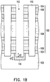
- FIG. 2 is a plan view of FIG. 1B .
- FIG. 3 is a plot of the impurity content in the substrate at the bottom of the slit as a function of the substrate depth after the slit etch is performed.
- slit etch In the process of forming a three-dimensional NAND memory with a vertical channel, slit etch, or called as deep trench etch, is used to create slits in a stacked structure, having silicon oxide layers and silicon nitride layers stacked alternately on a substrate, to divide channel pillars into groups.
- the aspect ratio of the slits is often higher than 30 and is defined to be a ratio of the total depth over the bottom critical dimension (BCD) of the slits.
- FIGS. 1A-1F are schematic cross-sectional views showing a manufacturing process of a semiconductor structure according to an embodiment of the invention.
- the semiconductor structure of the present invention can be used for a three-dimensional memory device, and therefore will be described below by accompanying with a manufacturing process of the three-dimensional memory device.
- a stacked structure 102 is first formed on a substrate 100 .
- the substrate 100 may be, for example, a single crystal silicon substrate. Doped regions (not shown in the figure) may be formed first in the substrate 100 , depending on design requirements.
- the stacked structure 102 includes a plurality of insulation layers 104 and a plurality of sacrificial layers 106 that are alternately stacked.
- the insulation layer 104 may be, for example, a silicon oxide layer
- the sacrificial layer 106 may be, for example, a silicon nitride layer.
- the sacrificial layers 106 will become formation regions of control gates in the process of forming the three-dimensional memory device, and the insulation layers 104 are used to isolate the control gates.
- the formation method of the insulation layers 104 and the sacrificial layers 106 may be, for example, chemical vapor deposition (CVD).
- the respective thicknesses of the insulation layers 104 and the sacrificial layers 106 may be adjusted according to actual needs.
- a plurality of channel holes 108 are formed to vertically penetrate the stacked structure 102 and extend into the substrate 100 having a first depth d 1 to expose the substrate 100 .
- the first depth d 1 is about 300-1500 ⁇ .
- the channel holes 108 are formed by, for example, forming a patterned hard mask layer (not shown in the figure) on the stacked structure 102 , and then performing an anisotropic etching process by using the hard mask layer as an etching mask. After the channel holes 108 are formed, the patterned hard mask layer is removed. Then, in each of the channel holes 108 , a bottom layer 100 f , such as a single crystal silicon layer, may be formed on the bottom of the channel holes 108 .
- a blocking insulation layer 110 a , a charge trapping layer 110 b , a tunneling insulation layer 110 c , a channel layer 110 d , and a core layer 110 e are sequentially formed along the sidewall, from the outside to the inside of the channel hole 108 , and a conductive plug 110 g is formed on the core layer 110 e to obtain the structure of the channel pillars 110 .
- the channel pillars 110 are also referred to as vertical channels (VCs).
- VCs vertical channels
- the blocking insulation layer 110 a , the charge trapping layer 110 b , the tunneling insulation layer 110 c , the channel layer 110 d , the core layer 110 e and the conductive plug 110 g above may be, for example, a silicon oxide layer, a silicon nitride layer, a silicon oxide layer, a polysilicon layer, a silicon oxide layer, and a doped polysilicon layer, respectively.
- FIG. 2 is the plan view of FIG. 1B
- FIG. 1B is the cross-sectional diagram of the cutting line I-I′.
- slit etch is performed to form a slit 112 extending through the stacked structure 102 and into the substrate 100 having a second depth d 2 to expose the substrate 100 , and the slits 112 separate adjacent two groups of the channel pillars 110 in FIG. 2 .
- the slits 112 typically has a height of at least 3 ⁇ m above the interface between the substrate 100 and the insulation layer 104 , and the second depth d 2 is about 100-500 ⁇ .
- the height of the slits 112 may be, for example, 3-12 ⁇ m, 3-10 ⁇ m, 3-8 ⁇ m, or 3-6 ⁇ m.
- the slits 112 have an aspect ratio of at least 30 and may be, for example, 30-60, 30-55, 30-50, 30-45 or 30-40.
- the slit etching is usually performed by dry etching using a plasma, and the gas source for generating the plasma may be, for example, a combination of various fluorinated carbon gases (e.g., CxFy), an oxygen-containing gas (e.g., O 2 or CO) and an inert gas (e.g., N 2 , He, Ar, or Kr).
- the applied electric field for accelerating the etching plasma needs to have a bias acceleration power of at least 9000 W (for example, 9000-15000 W, such as 9000, 10000, 11000, 12000, 13000, 14000, or 15000 W), and the plasma generator frequency is usually smaller than 60 MHz (for example, 0.4-60 MHz, such as 0.4, 0.8, 1, 5, 10, 15, 20, 25, 30, 35, 40, 45, 50, 55, or 60 MHz).
- the stacked structure 102 can be etched through to expose the surface of the substrate 100 .
- the third depth d 3 is usually less than 500 ⁇ , such as about 200 ⁇ , and the distribution profiles of the impurities concentrations in the substrate 100 are shown in FIG. 3 .
- FIG. 3 Please refer to FIG. 3 . It can be seen from FIG. 3 that there are mainly three kinds of impurities, i.e. oxygen, carbon and fluorine, and the distribution depth of these impurities can be more than 200 ⁇ .
- the sacrificial layers 106 between the insulation layers 104 are removed to form gaps 116 between adjacent insulation layers 104 .
- the method of removing the sacrificial layers 106 may be an isotropic etching, such as wet etching using H 3 PO 4 -based solution.
- a dielectric layer (not shown in figure) having a high dielectric constant and a metal barrier layer (not shown in figure) are sequentially formed on the exposed surfaces of the insulation layer 104 and the channel pillar 110 to surround the insulation layer 104 and the channel pillars 110 .
- a metal layer is formed to fill the gap 116 .
- the metal layer and the metal barrier layer are etched back to withdraw the metal layer and the metal barrier layer between the insulation layers 104 inward to form control gate layers 118 separated by the adjacent insulation layers 104 .
- the dielectric layer having a high dielectric constant above comprises a metal oxide, such as aluminum oxide, hafnium oxide, zirconium oxide, tantalum pentoxide, and any combinations thereof.
- the material of the metal barrier layer above may be, for example, cobalt, tantalum, niobium, tantalum nitride, indium oxide, tungsten nitride, titanium nitride or any combinations thereof.
- the material of the metal layer above is, for example, tungsten, molybdenum, ruthenium, cobalt, or aluminum, and the method of forming the metal layer may be, for example, chemical vapor deposition, or atomic layer deposition.
- isolating insulation layers 120 are formed on the inner surface of each of the slits 112 .
- the isolating insulation layers 120 cover the sidewalls of the insulation layers 104 and the control gate layers 118 , and also cover the surface of the substrate 100 exposed by the slits 112 .
- anisotropic etching is performed to etch the isolating insulation layers 120 covering the substrate 100 to form slit opening 122 having a width narrower than the width of the slit 112 and exposing the substrate 100 , and the slit opening 122 extends into the substrate 100 to a fourth depth d 4 of about 100-250 ⁇ .
- the material of the above-mentioned isolating insulation layer 120 may be, for example, silicon oxide.
- the method for forming the isolating insulation layer 120 may be, for example, chemical vapor deposition, and the anisotropic etching above may be, for example, dry etching.
- cleaning the impurity doped regions 114 is performed, and the clean plasma is used to remove the exposed impurity doped regions 114 located under the exposed surface of the substrate 100 to form a bottom opening 124 extending into the substrate 100 to a fifth depth d 5 .
- the fifth depth d 5 of the bottom opening 124 extending into the substrate 100 i.e. the height of the bottom opening 124 , is about 30-800 ⁇ , such as 30-700 ⁇ , 30-600 ⁇ , or 30-500 ⁇ , to adequately remove the impurity doped regions 114 under the exposed surface of the substrate 100 , so that the impurity concentration in the exposed surface layer of the substrate 100 may be significantly reduced to facilitate the later formation of metal silicide.
- the applied bias electric field used to accelerate the clean plasma should not be too large, and may be 30-100 W such as 90, 80, 70, 60, 50, 40, or 30 W, and the plasma generator frequency is 0.1-60 MHz, such as 0.1, 0.3, 0.5, 0.7, 0.9, 1.2, 1.5, 2, 5, 10, 15, 20, 25, 30, 40, 50, or 60 MHz. Therefore, the exposed surface layer of the substrate 100 may be prevented from being damaged again after the removal of the impurity doped regions 114 .
- the gas source of the clean plasma includes a halogen-containing gas, such as Cl 2 , Br 2 , or HBr, to react with carbon and silicon to form volatile gas products, such as CCl 4 , CBr 4 , SiCl 4 , and SiBr 4 , to be carried away.
- the clean plasma gas source may also include a hydrogen-containing gas, such as H 2 , to react with carbon, silicon, and fluorine to form volatile gas products, such as CH 4 , SiH 4 , and HF, to be carried away.
- the gas source of the clean plasma may also include an inert gas, such as N 2 , He or Ar, to be used as a carrier gas.
- a conductive plug 126 containing a metal barrier layer and a metal layer, is formed in the slit 112 , the slit opening 122 , and the bottom opening 124 to be used as a source line. It can be seen that the bottom end of the conductive plug 126 has a reduced neck structure 128 disposed in the slit opening 122 , and an enlarged bottom structure 130 disposed in the bottom opening 124 .
- the enlarged bottom structure 130 can increase the contact area of the conductive plug 126 and the substrate 100 to effectively reduce the contact resistance.
- the material of the metal barrier layer may include Ti, TiN, or a combination thereof, and the material of the metal layer may include tungsten.
- the conductive plugs 126 may be formed by first forming a metal barrier layer and a metal layer by chemical vapor deposition, and then removing the excess metal barrier layer and the excess metal layer by chemical mechanical polishing (CMP) to form the conductive plugs 126 .
- CMP chemical mechanical polishing
- a portion of the metal barrier layer contacting the substrate 100 may react with the substrate 100 to form metal silicide to further reduce the contact resistance between the conductive plugs 126 and the substrate 100 .
- the above embodiment of the present disclosure adds a step of using clean plasma to clean the impurity doped regions formed in the slit etching step to reduce the contact resistance between the conductive plugs and the substrate.
- a clean plasma can also be used to remove the impurities entering the substrate to solve the resistance increase problem.
Landscapes
- Semiconductor Memories (AREA)
- Non-Volatile Memory (AREA)
Abstract
Description
Claims (17)
Priority Applications (2)
| Application Number | Priority Date | Filing Date | Title |
|---|---|---|---|
| US16/371,579 US10770476B1 (en) | 2019-04-01 | 2019-04-01 | Semiconductor structure for three-dimensional memory device and manufacturing method thereof |
| CN201910336748.1A CN111769112B (en) | 2019-04-01 | 2019-04-25 | Semiconductor structure for three-dimensional memory element and manufacturing method thereof |
Applications Claiming Priority (1)
| Application Number | Priority Date | Filing Date | Title |
|---|---|---|---|
| US16/371,579 US10770476B1 (en) | 2019-04-01 | 2019-04-01 | Semiconductor structure for three-dimensional memory device and manufacturing method thereof |
Publications (2)
| Publication Number | Publication Date |
|---|---|
| US10770476B1 true US10770476B1 (en) | 2020-09-08 |
| US20200312866A1 US20200312866A1 (en) | 2020-10-01 |
Family
ID=72289938
Family Applications (1)
| Application Number | Title | Priority Date | Filing Date |
|---|---|---|---|
| US16/371,579 Active US10770476B1 (en) | 2019-04-01 | 2019-04-01 | Semiconductor structure for three-dimensional memory device and manufacturing method thereof |
Country Status (2)
| Country | Link |
|---|---|
| US (1) | US10770476B1 (en) |
| CN (1) | CN111769112B (en) |
Cited By (3)
| Publication number | Priority date | Publication date | Assignee | Title |
|---|---|---|---|---|
| US20210175249A1 (en) * | 2019-12-10 | 2021-06-10 | Micron Technology, Inc. | Integrated Assemblies Having One or More Modifying Substances Distributed Within Semiconductor Material, and Methods of Forming Integrated Assemblies |
| US11621273B2 (en) * | 2020-05-13 | 2023-04-04 | Micron Technology, Inc. | Integrated assemblies and methods of forming integrated assemblies |
| US12424282B2 (en) | 2022-05-24 | 2025-09-23 | Micron Technology, Inc. | Memory arrays comprising strings of memory cells and methods used in forming a memory array comprising strings of memory cells |
Citations (8)
| Publication number | Priority date | Publication date | Assignee | Title |
|---|---|---|---|---|
| US20110065270A1 (en) * | 2009-09-15 | 2011-03-17 | Sunil Shim | Three-dimensional semiconductor memory device and a method of fabricating the same |
| US20110086490A1 (en) | 2009-10-14 | 2011-04-14 | Inotera Memories, Inc. | Single-side implanting process for capacitors of stack dram |
| US9530789B2 (en) | 2014-05-02 | 2016-12-27 | Samsung Electronics Co., Ltd. | Semiconductor memory device and method of fabricating the same |
| US20170170190A1 (en) | 2015-12-15 | 2017-06-15 | Intel Corporation | Memory devices and systems having reduced bit line to drain select gate shorting and associated methods |
| US20170309638A1 (en) | 2016-04-25 | 2017-10-26 | Kabushiki Kaisha Toshiba | Semiconductor memory device and method for manufacturing same |
| US20180175050A1 (en) * | 2016-12-19 | 2018-06-21 | Young-Hwan Son | Vertical non-volatile memory device and method of manufacturing the same |
| US20190148401A1 (en) * | 2017-11-16 | 2019-05-16 | Yangtze Memory Technologies Co., Ltd. | Three-dimensional memory devices and fabricating methods thereof |
| US20190279996A1 (en) * | 2018-03-09 | 2019-09-12 | Toshiba Memory Corporation | Semiconductor device and method for manufacturing semiconductor device |
Family Cites Families (4)
| Publication number | Priority date | Publication date | Assignee | Title |
|---|---|---|---|---|
| KR20160080365A (en) * | 2014-12-29 | 2016-07-08 | 에스케이하이닉스 주식회사 | Electronic device and manufacturing method thereof |
| KR101944229B1 (en) * | 2015-11-20 | 2019-01-30 | 샌디스크 테크놀로지스 엘엘씨 | Three-dimensional NAND device including support pedestal structures for buried source lines and method of manufacturing the same |
| KR102607825B1 (en) * | 2016-01-18 | 2023-11-30 | 에스케이하이닉스 주식회사 | Semiconductor device and manufacturing method thereof |
| US9805805B1 (en) * | 2016-08-23 | 2017-10-31 | Sandisk Technologies Llc | Three-dimensional memory device with charge carrier injection wells for vertical channels and method of making and using thereof |
-
2019
- 2019-04-01 US US16/371,579 patent/US10770476B1/en active Active
- 2019-04-25 CN CN201910336748.1A patent/CN111769112B/en active Active
Patent Citations (15)
| Publication number | Priority date | Publication date | Assignee | Title |
|---|---|---|---|---|
| US20110065270A1 (en) * | 2009-09-15 | 2011-03-17 | Sunil Shim | Three-dimensional semiconductor memory device and a method of fabricating the same |
| US20110086490A1 (en) | 2009-10-14 | 2011-04-14 | Inotera Memories, Inc. | Single-side implanting process for capacitors of stack dram |
| TWI433274B (en) | 2009-10-14 | 2014-04-01 | 華亞科技股份有限公司 | Single-sided ion implantation process for stacked dynamic random access memory capacitors |
| US9530789B2 (en) | 2014-05-02 | 2016-12-27 | Samsung Electronics Co., Ltd. | Semiconductor memory device and method of fabricating the same |
| US9741734B2 (en) | 2015-12-15 | 2017-08-22 | Intel Corporation | Memory devices and systems having reduced bit line to drain select gate shorting and associated methods |
| WO2017105737A1 (en) | 2015-12-15 | 2017-06-22 | Intel Corporation | Memory devices and systems having reduced bit line to drain select gate shorting and associated methods |
| US20170170190A1 (en) | 2015-12-15 | 2017-06-15 | Intel Corporation | Memory devices and systems having reduced bit line to drain select gate shorting and associated methods |
| US20180130819A1 (en) | 2015-12-15 | 2018-05-10 | Intel Corporation | Memory devices and systems having reduced bit line to drain select gate shorting and associated methods |
| US10134758B2 (en) | 2015-12-15 | 2018-11-20 | Intel Corporation | Memory devices and systems having reduced bit line to drain select gate shorting and associated methods |
| US20170309638A1 (en) | 2016-04-25 | 2017-10-26 | Kabushiki Kaisha Toshiba | Semiconductor memory device and method for manufacturing same |
| US9929177B2 (en) | 2016-04-25 | 2018-03-27 | Toshiba Memory Corporation | Semiconductor memory device and method for manufacturing same |
| TWI624007B (en) | 2016-04-25 | 2018-05-11 | 東芝記憶體股份有限公司 | Semiconductor memory device and method of manufacturing same |
| US20180175050A1 (en) * | 2016-12-19 | 2018-06-21 | Young-Hwan Son | Vertical non-volatile memory device and method of manufacturing the same |
| US20190148401A1 (en) * | 2017-11-16 | 2019-05-16 | Yangtze Memory Technologies Co., Ltd. | Three-dimensional memory devices and fabricating methods thereof |
| US20190279996A1 (en) * | 2018-03-09 | 2019-09-12 | Toshiba Memory Corporation | Semiconductor device and method for manufacturing semiconductor device |
Cited By (7)
| Publication number | Priority date | Publication date | Assignee | Title |
|---|---|---|---|---|
| US20210175249A1 (en) * | 2019-12-10 | 2021-06-10 | Micron Technology, Inc. | Integrated Assemblies Having One or More Modifying Substances Distributed Within Semiconductor Material, and Methods of Forming Integrated Assemblies |
| US11056505B2 (en) * | 2019-12-10 | 2021-07-06 | Micron Technology, Inc. | Integrated assemblies having one or more modifying substances distributed within semiconductor material, and methods of forming integrated assemblies |
| US12144176B2 (en) | 2019-12-10 | 2024-11-12 | Lodestar Licensing Group Llc | Integrated assemblies having one or more modifying substances distributed within semiconductor material, and methods of forming integrated assemblies |
| US11621273B2 (en) * | 2020-05-13 | 2023-04-04 | Micron Technology, Inc. | Integrated assemblies and methods of forming integrated assemblies |
| US11844220B2 (en) | 2020-05-13 | 2023-12-12 | Micron Technology, Inc. | Integrated assemblies and methods of forming integrated assemblies |
| US12256546B2 (en) | 2020-05-13 | 2025-03-18 | Micron Technology, Inc. | Integrated assemblies and methods of forming integrated assemblies |
| US12424282B2 (en) | 2022-05-24 | 2025-09-23 | Micron Technology, Inc. | Memory arrays comprising strings of memory cells and methods used in forming a memory array comprising strings of memory cells |
Also Published As
| Publication number | Publication date |
|---|---|
| CN111769112B (en) | 2023-04-18 |
| CN111769112A (en) | 2020-10-13 |
| US20200312866A1 (en) | 2020-10-01 |
Similar Documents
| Publication | Publication Date | Title |
|---|---|---|
| TWI509746B (en) | Mosaic conductor for three-dimensional devices | |
| US12193213B2 (en) | Semiconductor structure and method of manufacturing same | |
| KR102824282B1 (en) | Methods of cutting a fine pattern, methods of forming active patterns using the same, and methods of manufacturing a semiconductor device using the same | |
| US10770476B1 (en) | Semiconductor structure for three-dimensional memory device and manufacturing method thereof | |
| CN110085551B (en) | Process for fabricating bit line of memory device, memory device and method of fabricating the same | |
| US7687341B2 (en) | Method for fabricating semiconductor device | |
| KR20210033388A (en) | Residue removal in metal gate cutting process | |
| KR100669103B1 (en) | Manufacturing Method of Flash Memory Device | |
| TWI701816B (en) | Semiconductor structure for three-dimensional memory device and manufacturing method thereof | |
| US20080160698A1 (en) | Method for fabricating a semiconductor device | |
| US12471345B2 (en) | Semiconductor device and method for manufacturing the same | |
| TWI855592B (en) | Semiconductor structures having deep trench capacitor and method for manufacturing the same | |
| CN112002673A (en) | Manufacturing method of isolation structure, DAC device and manufacturing method thereof | |
| US6969673B2 (en) | Semiconductor device with gate space of positive slope and fabrication method thereof | |
| US7435677B2 (en) | Method for fabricating semiconductor device | |
| KR102816863B1 (en) | Methods of manufacturing a vertical memory device | |
| KR100900237B1 (en) | Semiconductor device and manufacturing method thereof | |
| KR100667653B1 (en) | Semiconductor device and manufacturing method thereof | |
| CN120129228B (en) | Semiconductor structure and forming method thereof | |
| CN119136546B (en) | Methods for forming semiconductor structures | |
| CN113437015B (en) | Method for manufacturing semiconductor device | |
| CN119108270A (en) | Semiconductor structure and method for manufacturing the same | |
| KR100920043B1 (en) | Recess gate of semiconductor device and forming method thereof | |
| CN121487325A (en) | Dummy gate forming method and semiconductor device forming method | |
| TW202549520A (en) | Semiconductor device structure and method of forming the same |
Legal Events
| Date | Code | Title | Description |
|---|---|---|---|
| AS | Assignment |
Owner name: MACRONIX INTERNATIONAL CO., LTD., TAIWAN Free format text: ASSIGNMENT OF ASSIGNORS INTEREST;ASSIGNORS:CHUNG, YAO-AN;CHIU, YUAN-CHIEH;REEL/FRAME:048755/0480 Effective date: 20190329 |
|
| FEPP | Fee payment procedure |
Free format text: ENTITY STATUS SET TO UNDISCOUNTED (ORIGINAL EVENT CODE: BIG.); ENTITY STATUS OF PATENT OWNER: LARGE ENTITY |
|
| STCF | Information on status: patent grant |
Free format text: PATENTED CASE |
|
| MAFP | Maintenance fee payment |
Free format text: PAYMENT OF MAINTENANCE FEE, 4TH YEAR, LARGE ENTITY (ORIGINAL EVENT CODE: M1551); ENTITY STATUS OF PATENT OWNER: LARGE ENTITY Year of fee payment: 4 |