US10761619B2 - Touch-sensing system, display device, active pen, and pen recognition method - Google Patents
Touch-sensing system, display device, active pen, and pen recognition method Download PDFInfo
- Publication number
- US10761619B2 US10761619B2 US15/856,394 US201715856394A US10761619B2 US 10761619 B2 US10761619 B2 US 10761619B2 US 201715856394 A US201715856394 A US 201715856394A US 10761619 B2 US10761619 B2 US 10761619B2
- Authority
- US
- United States
- Prior art keywords
- pen
- panel
- pulse signal
- touch
- display device
- Prior art date
- Legal status (The legal status is an assumption and is not a legal conclusion. Google has not performed a legal analysis and makes no representation as to the accuracy of the status listed.)
- Active
Links
- 238000000034 method Methods 0.000 title claims abstract description 50
- 238000004891 communication Methods 0.000 claims description 101
- 230000005540 biological transmission Effects 0.000 claims description 57
- 238000012545 processing Methods 0.000 claims description 34
- 238000001514 detection method Methods 0.000 claims description 6
- 230000008054 signal transmission Effects 0.000 claims description 5
- 230000000630 rising effect Effects 0.000 claims description 3
- 230000000737 periodic effect Effects 0.000 claims description 2
- 230000008569 process Effects 0.000 abstract description 21
- 239000003990 capacitor Substances 0.000 description 9
- 238000001228 spectrum Methods 0.000 description 8
- 230000003071 parasitic effect Effects 0.000 description 7
- 230000008859 change Effects 0.000 description 5
- 238000010586 diagram Methods 0.000 description 4
- 238000002546 full scan Methods 0.000 description 4
- 230000007774 longterm Effects 0.000 description 4
- 238000005259 measurement Methods 0.000 description 4
- 238000010295 mobile communication Methods 0.000 description 2
- 238000011161 development Methods 0.000 description 1
- 230000000694 effects Effects 0.000 description 1
- 238000005516 engineering process Methods 0.000 description 1
- 239000004973 liquid crystal related substance Substances 0.000 description 1
- 238000012986 modification Methods 0.000 description 1
- 230000004048 modification Effects 0.000 description 1
- 230000002093 peripheral effect Effects 0.000 description 1
- 230000010363 phase shift Effects 0.000 description 1
- 238000000926 separation method Methods 0.000 description 1
- 238000006467 substitution reaction Methods 0.000 description 1
- 230000001360 synchronised effect Effects 0.000 description 1
- 230000002123 temporal effect Effects 0.000 description 1
Images


Classifications
-
- G—PHYSICS
- G06—COMPUTING; CALCULATING OR COUNTING
- G06F—ELECTRIC DIGITAL DATA PROCESSING
- G06F3/00—Input arrangements for transferring data to be processed into a form capable of being handled by the computer; Output arrangements for transferring data from processing unit to output unit, e.g. interface arrangements
- G06F3/01—Input arrangements or combined input and output arrangements for interaction between user and computer
- G06F3/03—Arrangements for converting the position or the displacement of a member into a coded form
- G06F3/033—Pointing devices displaced or positioned by the user, e.g. mice, trackballs, pens or joysticks; Accessories therefor
- G06F3/0354—Pointing devices displaced or positioned by the user, e.g. mice, trackballs, pens or joysticks; Accessories therefor with detection of 2D relative movements between the device, or an operating part thereof, and a plane or surface, e.g. 2D mice, trackballs, pens or pucks
- G06F3/03545—Pens or stylus
-
- G—PHYSICS
- G06—COMPUTING; CALCULATING OR COUNTING
- G06F—ELECTRIC DIGITAL DATA PROCESSING
- G06F3/00—Input arrangements for transferring data to be processed into a form capable of being handled by the computer; Output arrangements for transferring data from processing unit to output unit, e.g. interface arrangements
- G06F3/01—Input arrangements or combined input and output arrangements for interaction between user and computer
- G06F3/03—Arrangements for converting the position or the displacement of a member into a coded form
- G06F3/041—Digitisers, e.g. for touch screens or touch pads, characterised by the transducing means
- G06F3/0416—Control or interface arrangements specially adapted for digitisers
- G06F3/04162—Control or interface arrangements specially adapted for digitisers for exchanging data with external devices, e.g. smart pens, via the digitiser sensing hardware
-
- G—PHYSICS
- G06—COMPUTING; CALCULATING OR COUNTING
- G06F—ELECTRIC DIGITAL DATA PROCESSING
- G06F3/00—Input arrangements for transferring data to be processed into a form capable of being handled by the computer; Output arrangements for transferring data from processing unit to output unit, e.g. interface arrangements
- G06F3/01—Input arrangements or combined input and output arrangements for interaction between user and computer
- G06F3/03—Arrangements for converting the position or the displacement of a member into a coded form
- G06F3/041—Digitisers, e.g. for touch screens or touch pads, characterised by the transducing means
- G06F3/044—Digitisers, e.g. for touch screens or touch pads, characterised by the transducing means by capacitive means
- G06F3/0441—Digitisers, e.g. for touch screens or touch pads, characterised by the transducing means by capacitive means using active external devices, e.g. active pens, for receiving changes in electrical potential transmitted by the digitiser, e.g. tablet driving signals
-
- G—PHYSICS
- G06—COMPUTING; CALCULATING OR COUNTING
- G06F—ELECTRIC DIGITAL DATA PROCESSING
- G06F3/00—Input arrangements for transferring data to be processed into a form capable of being handled by the computer; Output arrangements for transferring data from processing unit to output unit, e.g. interface arrangements
- G06F3/01—Input arrangements or combined input and output arrangements for interaction between user and computer
- G06F3/03—Arrangements for converting the position or the displacement of a member into a coded form
- G06F3/041—Digitisers, e.g. for touch screens or touch pads, characterised by the transducing means
- G06F3/044—Digitisers, e.g. for touch screens or touch pads, characterised by the transducing means by capacitive means
- G06F3/0442—Digitisers, e.g. for touch screens or touch pads, characterised by the transducing means by capacitive means using active external devices, e.g. active pens, for transmitting changes in electrical potential to be received by the digitiser
-
- G—PHYSICS
- G08—SIGNALLING
- G08C—TRANSMISSION SYSTEMS FOR MEASURED VALUES, CONTROL OR SIMILAR SIGNALS
- G08C17/00—Arrangements for transmitting signals characterised by the use of a wireless electrical link
- G08C17/02—Arrangements for transmitting signals characterised by the use of a wireless electrical link using a radio link
-
- G—PHYSICS
- G06—COMPUTING; CALCULATING OR COUNTING
- G06F—ELECTRIC DIGITAL DATA PROCESSING
- G06F2203/00—Indexing scheme relating to G06F3/00 - G06F3/048
- G06F2203/038—Indexing scheme relating to G06F3/038
- G06F2203/0384—Wireless input, i.e. hardware and software details of wireless interface arrangements for pointing devices
-
- H—ELECTRICITY
- H04—ELECTRIC COMMUNICATION TECHNIQUE
- H04Q—SELECTING
- H04Q2213/00—Indexing scheme relating to selecting arrangements in general and for multiplex systems
- H04Q2213/13175—Graphical user interface [GUI], WWW interface, visual indication
Definitions
- the present disclosure relates to a display device, and more particularly, to a touch-sensing system, a display device, an active pen, and a pen recognition method.
- a display device that may provide a touch-based input scheme to allow a user to easily, intuitively, and conveniently input information or instructions, departing from the conventional input scheme using a button, a keyboard, or a mouse.
- the display device should be able to not only accurately sense a simple touch by a finger or a pen, but also perform accurate pen recognition for accurate location designation, movement trace input, and writing input.
- the present aspects may provide a touch-sensing system, a display device, an active pen, and a pen recognition method capable of performing rapid and accurate pen recognition.
- the present aspects may provide a touch-sensing system, a display device, an active pen, and a pen recognition method capable of simultaneously processing pen inputs through many active pens by distinguishably recognizing many active pens and distinguishably processing pen data of the many active pens.
- the present aspects may provide a touch-sensing system, a display device, an active pen, and a pen recognition method capable of transmitting and receiving reliable information required for pen recognition when a signal is transmitted and received between the active pen and the display device for pen recognition.
- the present aspects may provide a touch-sensing system, a display device, an active pen, and a pen recognition method capable of accurately and rapidly sensing a touch made with a finger and a touch with an active pen at the same time.
- the present aspects may provide a touch-sensing system including an active pen and a display device that includes a panel, on which a plurality of touch electrodes are arranged, and which performs pen recognition processing based on a link with the active pen.
- the active pen may radiate a pen pulse signal indicating pen identification information to the panel through a pen tip and wirelessly transmit pen data through an embedded pen wireless communication unit.
- the display device may include a touch-sensing circuit configured to supply a first panel-driving pulse signal to the panel and output raw data read from the panel, to which the pen pulse signal is radiated, a wireless communication module configured to receive and output the pen data wirelessly transmitted from the active pen, and a touch controller configured to acquire pen identification information from the raw data output from the touch-sensing circuit and perform pen recognition processing based on the acquired pen identification information and the pen data output from the wireless communication module.
- a touch-sensing circuit configured to supply a first panel-driving pulse signal to the panel and output raw data read from the panel, to which the pen pulse signal is radiated
- a wireless communication module configured to receive and output the pen data wirelessly transmitted from the active pen
- a touch controller configured to acquire pen identification information from the raw data output from the touch-sensing circuit and perform pen recognition processing based on the acquired pen identification information and the pen data output from the wireless communication module.
- the active pen may wirelessly transmit the pen identification information in addition to the pen data including one or more of a writing pressure, a pen inclination, and control information through the pen wireless communication unit.
- the wireless communication module of the display device may receive pen identification information and pen data and output the received pen identification information and pen data to the touch controller.
- the touch controller may perform pen recognition processing based on the raw data output from the touch-sensing circuit and the pen data and the pen identification information output from the wireless communication module.
- the present aspects may provide a display device configured to perform pen recognition processing based on a link with an active pen.
- the display may include a panel on which a plurality of touch electrodes are arranged, a touch-sensing circuit configured to, as a first panel-driving pulse signal is supplied to the panel, output raw data generated by reading a pen pulse signal, radiated from the active pen to the panel and indicating pen identification information, through the panel, a wireless communication module configured to receive and output pen data wirelessly transmitted from the active pen, and a touch controller configured to acquire pen identification information from the raw data output from the touch-sensing circuit and perform pen recognition processing based on the acquired pen identification information and the pen data output from the wireless communication module.
- the present aspects may provide a panel that includes a plurality of data lines arranged in a first direction, a plurality of gate lines arranged in a second direction, and a plurality of touch electrodes for touch sensing, and that links with an active pen.
- an image data signal may be applied to the plurality of data lines and a gate signal may be applied to the plurality of gate lines.
- a touch-driving section corresponding to a blank section between two display-driving sections, may include an uplink transmission section and a downlink transmission section.
- a first panel-driving pulse signal may be applied to all or some of the plurality of touch electrodes.
- a second panel-driving pulse signal or a third panel-driving pulse signal, distinguished from the first panel-driving pulse signal, may be applied to all or some of the plurality of touch electrodes.
- a signal corresponding to the first panel-driving pulse signal may be applied to all or some of the plurality of data lines.
- a signal corresponding to the first panel-driving pulse signal may be applied to all or some of the plurality of gate lines.
- the present aspects may provide an active pen that includes a pen tip in contact with or in proximity to a panel of the display device, an analog front-end receiver configured to receive a first panel-driving pulse signal supplied to the panel through the pen tip, an analog front-end transmitter configured to radiate a pen pulse signal indicating pen identification information through the pen tip based on the first panel-driving pulse signal, and a pen wireless communication unit configured to wirelessly transmit pen data.
- the pen wireless communication unit may wirelessly transmit the pen identification information in addition to the pen data.
- the present aspects may provide a pen recognition method including a step of supplying a first panel-driving pulse signal to a panel by the display device, a step of radiating a pen pulse signal indicating pen identification information to the panel through a pen tip based on the first panel-driving pulse signal and wirelessly transmitting pen data by the active pen, and a step of performing pen recognition processing based on raw data generated by being read from the panel, to which the pen pulse signal is radiated, and the pen data wirelessly transmitted from the active pen by the display device.
- the active pen may wirelessly transmit the pen identification information in addition to the pen data.
- the present aspects may provide a touch-sensing system including an active pen and a display device that includes a panel, on which a plurality of touch electrodes are arranged, and that performs pen recognition processing based on a link with the active pen.
- the active pen may radiate a pen pulse signal generated based on a first panel-driving pulse signal supplied to the panel and wirelessly transmit pen identification information through an embedded pen wireless communication unit.
- the display may include a touch-sensing circuit configured to supply a first panel-driving pulse signal to the panel and output raw data read from the panel, to which the pen pulse signal is radiated, a wireless communication module configured to receive and output the pen identification information wirelessly transmitted from the active pen, and a touch controller configured to perform pen recognition processing based on the raw data output from the touch-sensing circuit and the pen identification information output from the wireless communication module.
- a touch-sensing circuit configured to supply a first panel-driving pulse signal to the panel and output raw data read from the panel, to which the pen pulse signal is radiated
- a wireless communication module configured to receive and output the pen identification information wirelessly transmitted from the active pen
- a touch controller configured to perform pen recognition processing based on the raw data output from the touch-sensing circuit and the pen identification information output from the wireless communication module.
- the pen pulse signal radiated from the active pen may not include the pen identification information.
- the pen pulse signal radiated from the active pen may include the pen identification information.
- the active pen may wirelessly transmit pen data in addition to the pen identification information through the embedded pen wireless communication unit.
- FIG. 1 illustrates a touch-sensing system according to the present disclosure
- FIG. 2 illustrates an operation mode of a display device according to the present disclosure
- FIG. 3 is a block diagram illustrating a display device according to the present disclosure
- FIG. 4 is a block diagram illustrating an active pen according to the present disclosure
- FIG. 5 illustrates a pen recognition process according to the present disclosure
- FIG. 6 illustrates a first panel-driving pulse signal supplied to a panel, a pen pulse signal radiated from an active pen, a read value generated by reading the pen pulse signal from a touch-sensing circuit, and pen identification information according to a sign of the read value according to the present disclosure
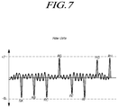
- FIG. 7 illustrates raw data acquired through reading a panel by a touch-sensing circuit of a display device according to the present disclosure
- FIG. 8 illustrates display-driving elements in the case in which a panel of a display device is a display panel including a touch screen panel therein according to the present disclosure
- FIG. 9 illustrates an uplink and a downlink between a display device and an active pen according to the present disclosure
- FIG. 10 illustrates operation sections of a display device according to the present disclosure
- FIG. 11 illustrates three panel-driving pulse signals supplied to panel of a display device according to the present disclosure
- FIGS. 12A and 12B illustrate examples of a touch process of a display device according to the present disclosure
- FIGS. 13 to 15 illustrate a wireless communication method between an active pen and a display device according to the present disclosure
- FIG. 16 is a flowchart illustrating a pen recognition method according to the present disclosure.
- FIG. 17 illustrates another pen recognition process according to the present disclosure.
- FIG. 18 illustrates multi-pen recognition according to the present disclosure.
- first, second, A, B, (a), (b) or the like may be used herein when describing components of the present disclosure.
- Each of these terminologies is not used to define an essence, order or sequence of a corresponding component but used merely to distinguish the corresponding component from other component(s).
- another structural element may “be connected to”, “be coupled to”, or “be in contact with” the structural elements as well as that the certain structural element is directly connected to or is in direct contact with another structural element.
- FIG. 1 illustrates a touch-sensing system according to the present disclosure
- FIG. 2 illustrates an operation mode of a display device 10 according to the present disclosure.
- the touch-sensing system includes an active pen 20 and the display device 10 for processing pen recognition through a link with the active pen 20 .
- the display device 10 may have a display mode for displaying an image and a touch-sensing mode for sensing a touch.
- the display device 10 may sense not only a touch by a finger but also a touch by the active pen 20 in the touch-sensing mode.
- the display device 10 may link with the active pen 20 and sense the touch by the active pen 20 .
- the active pen 20 is a pen that includes an electrical component and performs an active operation of linking with the display device 10 in connection with the touch sensing.
- the display device 10 may sense a touch by a passive pen that merely acts as a capacitor, like a finger, without an operation of actively linking with the display device 10 .
- the touch by the passive pen is processed in the same manner as the touch by the finger. Accordingly, in this application, the touch by the finger includes the touch by the passive pen.
- the present disclosure provides a pen recognition method by which the display device 10 may efficiently recognize the active pen 20 and simultaneously recognize many active pens 20 .
- the active pen 20 may provide pen identification information to the display device 10 through a predetermined path (at least one of a wireless communication path and a path through a panel), so that it is possible to perform rapid and accurate pen recognition and also distinguishably recognize multiple active pens 20 so as to simultaneously process pen inputs made through the multiple active pens 20 .
- a predetermined path at least one of a wireless communication path and a path through a panel
- the active pen 20 provides pen identification information to the display device 10 through a panel in the form of a radiated signal will be described.
- the display device 10 supplies a first panel-driving pulse signal to a panel 310 (shown in FIG. 3 ). Accordingly, the active pen 20 radiates a pen pulse signal (PENS) indicating pen identification information to the panel of the display device 10 through a pen tip 410 (shown in FIG. 4 ) based on the first panel-driving pulse signal supplied to the panel 310 .
- PNS pen pulse signal
- the active pen 20 wirelessly transmits pen data to the display device 10 .
- the active pen 20 wirelessly and additionally transmits pen identification information to the display device 10 .
- the display device 10 generates raw data read from the panel, to which the pen pulse signal has been radiated.
- the display device 10 receives the pen data wirelessly transmitted from the active pen 20 .
- the display device 10 may acquire the pen identification information from the generated raw data and perform pen recognition processing based on the acquired pen identification information and the wirelessly received pen data.
- the pen recognition may mean that the display device 10 recognizes the presence of the active pen 20 (that is, the generation of a touch by the active pen 20 ) and may further mean that the display device 10 recognizes pen identification information of the active pen 20 .
- the recognition of the active pen 20 by the display device 10 may further mean that the display device 10 detects a location (pen location) of the touch made by the active pen 20 .
- the recognition of the active pen 20 by the display device 10 may further mean that the display device 10 recognizes additional pen information such as writing pressure or the inclination of the active pen 20 .
- the display device 10 may sense the same as a touch. Further, in the case in which the finger or the active pen 20 is in proximity to the panel within a predetermined range or closer without contacting the panel, the display device 10 may sense the same as a touch. That is, the display device 10 according to the present aspects may provide both contact-type touch sensing and non-contact-type touch sensing (touch sensing through hovering).
- FIG. 3 is a diagram illustrating the display device 10 according to the present aspects.
- the display device 10 is a device for linking with the active pen 20 and performing pen recognition processing, and may include a panel 310 , a touch-sensing circuit 320 , a touch controller 330 , and a wireless communication module 300 .
- a plurality of touch electrodes may be arranged and a plurality of touch lines (TLs) for electrically connecting the plurality of touch electrodes (TEs) and the touch-sensing circuit 320 may be arranged.
- the touch-sensing circuit 320 supplies a first panel-driving pulse signal (LFD) to all or some of the plurality of touch electrodes (TEs) arranged on the panel 310 and generates raw data (also referred to as sensing data) containing a read value that is read through each touch electrode (TE).
- LFD first panel-driving pulse signal
- the touch-sensing circuit 320 may include, for example, a preamplifier for receiving the first panel-driving pulse signal (LFD) to supply the received first panel-driving pulse signal (LFD) to the panel 310 and receiving a signal from the panel 310 to output the received signal, at least one sensing unit including an integrator for integrating and outputting the signal output from the preamplifier, and an analog-to-digital converter for converting the signal output from the integrator within at least one sensing unit into a digital value and outputting a read value corresponding to the digital value.
- a preamplifier for receiving the first panel-driving pulse signal (LFD) to supply the received first panel-driving pulse signal (LFD) to the panel 310 and receiving a signal from the panel 310 to output the received signal
- at least one sensing unit including an integrator for integrating and outputting the signal output from the preamplifier, and an analog-to-digital converter for converting the signal output from the integrator within at least
- the touch-sensing circuit 320 may further include a multiplexer circuit for making a selective electrical connection between at least one sensing unit and the plurality of touch lines (TLs) arranged on the panel 310 .
- the touch-sensing circuit 320 may further include a multiplexer circuit for making a selective electrical connection between at least one sensing unit and the analog-to-digital converter.
- the read value that is read through each touch electrode (TE) may include information corresponding to capacitance formed between each touch electrode (TE) and the active pen 20 or a change in the capacitance, or information corresponding to capacitance formed between each touch electrode (TE) and the finger or a change in the capacitance.
- the read value may vary depending on each touch electrode (TE). That is, the size of the read value may vary depending on how close the finger or the active pen 20 is to the corresponding touch electrode (TE).
- the raw data (containing read values) generated by the touch-sensing circuit 320 may be transmitted to the touch controller 330 through an interface between the touch-sensing circuit 320 and the touch controller 330 .
- the interface between the touch-sensing circuit 320 and the touch controller 330 may be, for example, a Serial Peripheral Interface (SPI).
- SPI Serial Peripheral Interface
- the touch controller 330 may sense the presence or absence of the touch by the finger or the active pen 20 based on the raw data generated by the touch-sensing circuit 320 , or may sense a touch location.
- the wireless communication module 300 is an element for performing wireless communication with the active pen 20 , and may be a short-range wireless communication module using Bluetooth, Near-Field Communication (NFC), Radio-Frequency Identification (RFID), or direct Wi-Fi, or a wireless communication module, such as one using Wi-Fi, or may further include a mobile communication module, such as one using Long Term Evolution (LTE).
- the wireless communication module 300 may be a small and low-power communication module.
- FIG. 4 is a block diagram illustrating the active pen 20 according to the present aspects.
- the active pen 20 may include a pen tip 410 that is in contact with or in proximity to the panel 310 of the display device 10 , an analog front-end receiver (AFE RX) 420 for receiving a signal through the pen tip 410 , an analog front-end transmitter (AFE TX) 430 for radiating a signal through the pen tip 410 , a pen wireless communication unit 400 , a battery 450 , and a pen controller 440 for generating a signal, controlling signal transmission/reception, and controlling the overall function.
- AFE RX analog front-end receiver
- AFE TX analog front-end transmitter
- the pen wireless communication unit 400 is an element for performing wireless communication with the wireless communication module 300 of the display device 10 , and may be a short-range wireless communication module using Bluetooth, Near-Field Communication (NFC), Radio-Frequency Identification (RFID), or direct Wi-Fi, or a wireless communication module, such as one using Wi-Fi, or may further include a mobile communication module, such as one using Long Term Evolution (LTE).
- NFC Near-Field Communication
- RFID Radio-Frequency Identification
- LTE Long Term Evolution
- FIG. 5 illustrates a pen recognition process according to the present aspects.
- FIG. 6 illustrates a first panel-driving pulse signal (LFD) supplied to the panel 310 , a pen pulse signal (PENS) radiated from the active pen 20 , a read value generated by reading the pen pulse signal (PENS) from the touch-sensing circuit 320 , and pen identification information according to a sign of the read value in the touch-sensing system according to the present aspects.
- LFD panel-driving pulse signal
- PNS pen pulse signal
- FIG. 7 illustrates raw data acquired by reading the panel 310 by the touch-sensing circuit 320 of the display device 10 according to the present aspects.
- the touch-sensing circuit 320 supplies the first panel-driving pulse signal (LFD) to the panel 310 . Accordingly, the analog front-end receiver 420 of the active pen 20 receives the first panel-driving pulse signal (LFD) supplied to the panel 310 through the pen tip 410 in S 10 .
- the analog front-end transmitter 430 of the active pen 20 radiates the pen pulse signal (PENS) indicating pen identification information (pen ID) to the panel 310 through the pen tip 410 based on the first panel-driving pulse signal (LFD) in S 20 - 1 .
- PNS pen pulse signal
- pen ID pen identification information
- LFD first panel-driving pulse signal
- the pen wireless communication unit 400 of the active pen 20 may wirelessly transmit pen data containing one or more pieces of pen-related additional information in S 20 - 2 .
- the touch-sensing circuit 320 may generate raw data containing the read values generated by reading, through the panel 310 , the pen pulse signal (PENS) indicating the pen identification information and output the generated raw data to the touch controller 330 in S 30 - 1 .
- the pen pulse signal (PENS) indicating the pen identification information
- the wireless communication module 300 may receive the pen data wirelessly transmitted from the active pen 20 and output the pen data to the touch controller 330 in S 30 - 2 .
- the touch controller 330 may acquire pen identification information (pen ID) from the raw data output from the touch-sensing circuit 320 and perform pen recognition processing based on the acquired pen identification information and the pen data output from the wireless communication module 300 in S 40 .
- pen ID pen identification information
- the touch controller 330 may acquire pen identification information (pen ID) from the raw data output from the touch-sensing circuit 320 and sense a touch location (pen location) of the active pen 20 corresponding to the acquired pen identification information.
- the touch controller 330 may further recognize additional pen information of the active pen 20 based on the pen data output from the wireless communication module 300 .
- the pen data may contain one or more pieces of additional pen information, such as a writing pressure, a pen inclination, control information, and button input information.
- additional pen information such as a writing pressure, a pen inclination, control information, and button input information.
- the touch controller 330 may sense a touch location of the finger (finger location) based on the raw data output from the touch-sensing circuit 320 .
- the display device 10 acquires the pen identification information of the active pen 20 through the panel 310 and acquires the pen data of the active pen 20 through a wireless communication path. That is, the display device 10 may acquire information required for pen recognition (pen identification information and pen data) through two paths.
- the active pen 20 may transmit the pen data and the pen identification information, which is a large amount of data, to the display device 10 through two different respective paths. Therefore, the display device 10 may rapidly and accurately acquire information required for pen recognition processing (additional pen information within pen data, and pen identification information), thereby rapidly and accurately performing pen recognition processing.
- the display device 10 may distinguish between a plurality of active pens 20 and may thus provide multi-pen recognition.
- the active pen 20 may further wirelessly transmit pen identification information (pen ID) as well as pen data containing one or more of a writing pressure, a pen inclination, and control information through the pen wireless communication unit 400 .
- pen ID pen identification information
- pen data containing one or more of a writing pressure, a pen inclination, and control information
- the wireless communication module 300 of the display device 10 receives the pen identification information and the pen data and outputs the received pen identification information and pen data to the touch controller 330 in S 30 - 2 .
- the touch controller 330 may perform pen recognition processing based on the raw data output from the touch-sensing circuit 320 , the pen data, and the pen identification information output from the wireless communication module 300 in S 40 .
- the pen identification information may be transmitted to the touch controller 330 through the panel 310 , or may be transmitted to the touch controller 330 through a wireless transmission scheme. That is, the touch controller 330 may acquire the pen identification information (pen ID) through two paths.
- the touch controller 330 may reliably acquire the pen identification information, which is important information that makes multi-pen recognition possible. Accordingly, the display device 10 may more accurately recognize the active pen 20 , and may accurately distinguish between two or more active pens 20 and simultaneously provide pen recognition processing thereof. Accordingly, the user may perform touch, writing, or input by simultaneously using two or more active pens 20 .
- a first panel-driving pulse signal is a signal for driving the panel 310 to sense the touch by the finger or the active pen 20 , that is, the signal that the touch-sensing circuit 320 supplies to the panel 310 .
- the first panel-driving pulse signal may include a plurality of panel-driving pulses A, B, C, D, E, F, G, and H.
- the active pen 20 receives the first panel-driving pulse signal (LFD) supplied to the panel 310 through the pen tip 410 and generates a pen pulse signal (PENS) based on the received first panel-driving pulse signal (LFD).
- LFD first panel-driving pulse signal
- PNS pen pulse signal
- the pen pulse signal is a signal that allows the display device 10 to recognize the active pen 20 , that is, a signal that the active pen 20 radiates to the panel 310 of the display device 10 .
- the active pen 20 generates the pen pulse signal (PENS) based on the first panel-driving pulse signal (LFD).
- the pen pulse signal may include a plurality of pen pulses PA, PB, PC, PD, PE, PF, PG, and PH indicating a plurality of digital codes (for example, 0, 0, 0, 1, 0, 0, 1, 1) corresponding to pen identification information based on the first panel-driving pulse signal (LFD).
- the plurality of pen pulses PA, PB, PC, PD, PE, PF, PG, and PH included in the pen pulse signal may include first pen pulses (for example, PA, PB, PC, PE, and PF) indicating a first digital code (for example, 0 or 1) and second pen pulses (for example, PD, PG, and PH) indicating a second digital code (for example, 1 or 0).
- first pen pulses for example, PA, PB, PC, PE, and PF
- second pen pulses for example, PD, PG, and PH
- the first pen pulses (for example, PA, PB, PC, PE, and PF) are pulsed at rising time of corresponding panel-driving pulses (for example, A, B, C, E, and F) among the plurality of panel-driving pulses A, B, C, D, E, F, G, and H included in the first panel-driving pulse signals (LFD).
- panel-driving pulses for example, A, B, C, E, and F
- the second pen pulses (for example, PD, PG, and PH) are pulsed at falling time of corresponding panel-driving pulses (for example, D, G, and F) among the plurality of panel-driving pulses A, B, C, D, E, F, G, and H included in the first panel-driving pulse signals (LFD).
- corresponding panel-driving pulses for example, D, G, and F
- the display device 10 may accurately read the pen pulse signal (PENS) and accurately recognize the pen identification information (PID) indicated by the pen pulse signal (PENS).
- the raw data read from the panel 310 by the touch-sensing circuit 320 may include a plurality of read values (for example, RA, RB, RC, RD, RE, RF, RG, and RH) having a real number within a range greater than or equal to ⁇ N (N is a preset positive real number) and less than or equal to +P (P is a preset positive real number).
- the plurality of read values may include first read values (for example, RA, RB, RC, RE, and RF) for the first pen pulses (for example, PA, PB, PC, PE, and PF) and second read values (for example, RD, RG, and RH) for the second pen pulses (for example, PD, PG, and PH), and the signs of the first read values (RA, RB, RC, RE, and RF) may be different from the signs of the second read values (for example, RD, RG, and RH).
- first read values for example, RA, RB, RC, RE, and RF
- first pen pulses for example, PA, PB, PC, PE, and PF
- second read values for example, RD, RG, and RH
- the signs of the first read values RA, RB, RC, RE, and RF
- the corresponding first read values for example, RA, RB, RC, RE, and RF
- ⁇ real negative
- the touch controller 330 may determine that the corresponding first read values (for example, RA, RB, RC, RE, and RF) having the real negative ( ⁇ ) value correspond to the first digital code (for example, 0).
- the corresponding first read values for example, RA, RB, RC, RE, and RF
- the real negative ( ⁇ ) value correspond to the first digital code (for example, 0).
- the corresponding second read values (for example, RD, RG, and RH) have a positive (+) real number.
- the touch controller 330 may determine that the corresponding second read values (for example, RD, RG, and RH) having the positive (+) real number correspond to the second digital code (for example, 1).
- the touch controller 330 may determine a plurality of digital codes (for example, 00010011) based on the sign of each of the plurality of read values (for example, RA, RB, RC, RD, RE, RF, RG, and RH) included in the raw data read from the panel 310 by the touch-sensing circuit 320 and acquire the pen identification information (PID) including the plurality of determined digital codes (for example, 00010011).
- PID pen identification information
- PID pen identification information
- the raw data read from the panel 310 by the touch-sensing circuit 320 may include a plurality of read values (for example, RA, RB, RC, RD, RE, RF, RG, and RH) having real numbers within a range greater than or equal to ⁇ N (where N is a preset positive real number) and less than or equal to +P (where P is a preset positive real number).
- the raw data may include a plurality of read values (for example, RA, RB, RC, RD, RE, RF, RG, and RH) having a real number within a range greater than or equal to ⁇ 1 and less than or equal to +1.
- a plurality of read values for example, RA, RB, RC, RD, RE, RF, RG, and RH
- the touch controller 330 may detect a location of the active pen 20 or the finger or the presence or absence of the touch based on the distribution of all or some of the plurality of read values (for example, RA, RB, RC, RD, RE, RF, RG, and RH) on the panel 310 .
- the plurality of read values for example, RA, RB, RC, RD, RE, RF, RG, and RH
- the touch controller 330 may calculate the distribution of the read values (i.e. the distribution of the sizes of the read values at each panel location) having the real number based on the received and collected raw data, and when a distribution appears such that read values are significantly different at a particular location based on the calculated distribution, the particular location may be detected to indicate the presence or absence of the touch by the finger or the active pen 20 and/or the touch location.
- the distribution of the read values i.e. the distribution of the sizes of the read values at each panel location
- the touch controller 330 may acquire the pen identification information (PID) of the active pen 20 based on the raw data read from the panel 310 by the touch-sensing circuit 320 and may also detect the touch location of the active pen 20 . In some cases, the touch controller 330 may detect the presence or absence of the touch by the finger and/or the touch location.
- PID pen identification information
- the panel 310 of the display device 10 may be a touch screen panel dedicated for touch sensing or, in some cases, may be a display panel serving as the touch screen panel.
- FIG. 8 illustrates display-driving elements in the case in which the panel 310 of the display device 10 according to the present aspects is a display panel including a touch screen panel therein.
- the panel 310 of the display device 10 when the panel 310 of the display device 10 according to the present aspects is a display panel including a touch screen panel therein, a plurality of data lines (DLs) in a first direction (for example, a column direction), a plurality of gate lines (GLs) in a second direction (for example, a row direction), and a plurality of touch electrodes (TEs) for touch sensing may be arranged on the panel 310 .
- the panel 310 including the touch screen panel therein means that a plurality of touch electrodes (TEs) is embedded into and arranged on the panel 310 .
- the display device 10 may include a data-driving circuit 810 for driving a plurality of data lines (DLs) and a gate-driving circuit 820 for driving a plurality of gate lines (GLs).
- DLs data lines
- GLs gate lines
- the display device 10 may further include a control element, such as a timing controller for controlling the data-driving circuit 810 and the gate-driving circuit 820 .
- a control element such as a timing controller for controlling the data-driving circuit 810 and the gate-driving circuit 820 .
- the data-driving circuit 810 and the touch-sensing circuit 320 may be combined into and implemented as a single integrated circuit.
- two or more of the data-driving circuit 810 , the gate-driving circuit 820 , the timing controller, the touch-sensing circuit 320 , and the touch controller 330 may be combined into and implemented as a single integrated circuit.
- FIG. 9 illustrates an uplink and a downlink between the display device 10 and the active pen 20 according to the present aspects.
- the display device 10 and the active pen 20 transmit and receive a signal for pen recognition.
- the display device 10 transmits a signal (including all types of data and information) to the active pen 20 , an uplink exists between the display device 10 and the active pen 20 .
- a downlink exists between the display device 10 and the active pen 20 .
- FIG. 10 illustrates operation sections of the display device 10 according to the present aspects
- FIG. 11 illustrates three panel-driving pulse signals supplied to the panel 310 of the display device 10 according to the present aspects.
- the operation sections of the display device 10 may include a display-driving section and a touch-driving section.
- the display device 10 may alternately perform display driving and touch driving.
- the touch-driving section may correspond to a blank time between two display-driving sections.
- an image data signal is applied to a plurality of data lines (DLs) and a gate signal is applied to a plurality of gate lines (GLs) on the panel 310 .
- the touch-driving section may include an uplink transmission section (ULNK) for transmitting a signal from the display device 10 to the active pen 20 and a downlink transmission section (DLNK) for transmitting a signal from the active pen 20 to the display device 10 .
- ULNK uplink transmission section
- DLNK downlink transmission section
- a first panel-driving pulse signal may be applied to all or some of a plurality of touch electrodes (TEs) on the panel 310 .
- a second panel-driving pulse signal (BCON) or a third panel-driving pulse signal (PNG) may be applied to all or some of a plurality of touch electrodes (TEs) on the panel 310 .
- the second panel-driving pulse signal (BCON) or the third panel-driving pulse signal (PNG) is a signal distinguished from the first panel-driving pulse signal (LFD).
- the panel status is a status in which the first panel-driving pulse signal (LFD) is supplied to the panel 310 . Accordingly, the first panel-driving pulse signal (LFD) supplied to the panel 310 is input into the active pen 20 .
- the pen pulse signal (PENS), indicating pen identification information, is radiated to the panel 310 from the active pen 20 .
- pen identification information and pen data are wirelessly transmitted to the wireless communication module 300 from the active pen 20 .
- a finger location (FLOC) at which the touch by the finger is performed may be detected
- a pen location (PLOC) at which the touch by the active pen 20 is performed may be detected
- pen identification information (PID) of the active pen 20 may be detected.
- the panel status is a status in which the second panel-driving pulse signal (BCON) or the third panel-driving pulse is supplied to the panel 310 .
- the second panel-driving pulse signal (BCON) or the third panel-driving pulse supplied to the panel 310 may be input into the active pen 20 from the panel 310 .
- the second panel-driving pulse signal (BCON) or the third panel-driving pulse signal supplied to the panel 310 and transmitted to the active pen 20 in the uplink transmission section (ULNK) may be distinguished from the first panel-driving pulse signal (LFD) supplied to the panel 310 and transmitted to the active pen 20 in the downlink transmission section (DLNK).
- the touch-driving section As described above, by dividing the touch-driving section into the uplink transmission section (ULNK) and the downlink transmission section (DLNK), it is possible to realize a proper panel-driving state required for pen recognition with respect to each of the uplink transmission section (ULNK) and the downlink transmission section (DLNK). Accordingly, efficient and accurate signal transmission/reception for pen recognition is possible, and as a result, accurate and efficient pen recognition is possible.
- the three panel-driving pulse signals (LFD, BCON, and PNG) may be supplied to the panel 310 .
- the first panel-driving pulse signal (LFD) is a signal supplied to the panel 310 and transmitted to the active pen 20 in the downlink transmission section (DLNK), that is, a signal having a periodic pattern in which a high-level section (HL) and a low-level section (LL) alternate.
- DLNK downlink transmission section
- the active pen 20 may generate a pen pulse signal (PENS) indicating pen identification information at pulse timing of the first panel-driving pulse signal (LFD) and radiate the generated pen pulse signal (PENS) to the panel 310 .
- PNS pen pulse signal
- the first panel-driving pulse signal (LFD) merely swings alternately in the high-level section (HL) and the low-level section (LL), but no meaningful information is carried thereon.
- the second panel-driving pulse signal (BCON) and the third panel-driving pulse signal (PNG) are signals that carry meaningful information.
- the second panel-driving pulse signal (BCON) is a signal supplied to the panel 310 and transmitted to the active pen 20 in the uplink transmission section (ULNK), that is, a beacon signal carrying panel information.
- the active pen 20 may recognize that the panel 310 is in proximity to the active pen 20 and be made aware of panel information of the recognized panel 310 .
- BCON the second panel-driving pulse signal
- the panel information may include panel identification information, a panel resolution, and a panel manufacturer.
- the third panel-driving pulse signal is a signal supplied to the panel 310 and transmitted to the active pen 20 in the uplink transmission section (ULNK), that is, a ping signal carrying touch-driving section information.
- the active pen 20 may operate based on synchronization with the driving operation of the display device 10 or the panel 310 .
- PNG panel-driving pulse signal
- the active pen 20 may recognize the frame that the display device 10 is driving through the third panel-driving pulse signal (PNG), corresponding to the ping signal, and recognize a touch-driving section within the frame.
- PNG panel-driving pulse signal
- the third panel-driving pulse signal may temporally synchronize the operation between the display device 10 and the active pen 20 .
- first panel-driving pulse signal LFD
- second panel-driving pulse signal BCON
- third panel-driving pulse signal PNG
- the touch sensing may be accurately performed.
- the three panel-driving pulse signals may be basically supplied to all or some of the plurality of touch electrodes (TEs) arranged on the panel 310 .
- an unnecessary parasitic capacitor may be formed between the touch electrodes (TEs) and other electrodes within the panel 310 .
- the parasitic capacitor may be a factor that causes a Resistor-Capacitor (RC) delay for the touch electrodes (TEs) and deteriorates sensing accuracy in capacitance-based touch sensing.
- RC Resistor-Capacitor
- a signal corresponding to the first panel-driving pulse signal (LFD) may be applied to all or some of the plurality of data lines (DLs).
- a signal corresponding to the first panel-driving pulse signal (LFD) may be applied to all or some of the plurality of gate lines (GLs).
- the signal corresponding to the first panel-driving pulse signal (LFD) may be a signal that is completely the same as or is substantially the same as the first panel-driving pulse signal (LFD) based on frequency, amplitude, phase, and other signal characteristics.
- the signal corresponding to the first panel-driving pulse signal (LFD) may be a signal that is completely the same as or substantially the same as the first panel-driving pulse signal (LFD) based on at least one of the frequency, amplitude, phase, and other signal characteristics.
- the term “substantially the same” means that two values are not exactly the same as each other, but they are considered to be the same when the difference therebetween is within a predetermined tolerance margin or a measurement error range.
- the tolerance margin or the measurement error range may be ⁇ 20%, ⁇ 10%, ⁇ 5%, or ⁇ 1%.
- a finger location (FLOC), at which the touch by the finger is performed, may be accurately detected
- a pen location (PLOC), at which the touch by the active pen 20 is performed may be accurately detected
- pen identification information (PID) of the active pen 20 may be accurately detected in the state in which the effect of the parasitic capacitor is removed or substantially removed.
- the term “substantial removal of the parasitic capacitor” may mean that the parasitic capacitor is considered to be removed when a change in touch-sensing accuracy attributable to the parasitic capacitor is within a predetermined tolerance margin (for example, ⁇ 20%, ⁇ 10%, ⁇ 5%, or ⁇ 1%) even if the parasitic capacitor is not completely removed.
- a predetermined tolerance margin for example, ⁇ 20%, ⁇ 10%, ⁇ 5%, or ⁇ 1%
- a signal corresponding to the second panel-driving pulse signal (BCON) may be applied to all or some of the plurality of data lines (DLs) while the second panel-driving pulse signal (BCON) is supplied to the panel 310 .
- a signal corresponding to the second panel-driving pulse signal (BCON) may be applied to all or some of the plurality of gate lines (GLs) while the second panel-driving pulse signal (BCON) is supplied to the panel 310 .
- a signal corresponding to the third panel-driving pulse signal (PNG) may be applied to all or some of the plurality of data lines (DLs) while the third panel-driving pulse signal (PNG) is supplied to the panel 310 .
- a signal corresponding to the third panel-driving pulse signal (PNG) may be applied to all or some of the plurality of gate lines (GLs) while the third panel-driving pulse signal (PNG) is supplied to the panel 310 .
- the signal corresponding to the second panel-driving pulse signal (BCON) or the third panel-driving pulse signal (PNG) may be a signal that is completely the same as or substantially the same as the second panel-driving pulse signal (BCON) or the third panel-driving pulse signal (PNG) based on frequency, amplitude, phase, or other signal characteristics.
- the signal corresponding to the second panel-driving pulse signal (BCON) or the third panel-driving pulse signal (PNG) may be a signal that is completely the same as or substantially the same as the second panel-driving pulse signal (BCON) or the third panel-driving pulse signal (PNG) based on at least one of the frequency, amplitude, phase, or other signal characteristics.
- the term “substantially the same” means that two values are not exactly the same as each other, but they are considered to be the same when the difference therebetween is within a predetermined tolerance margin or measurement error range.
- the tolerance margin or the measurement error range may be ⁇ 20%, ⁇ 10%, ⁇ 5%, or ⁇ 1%.
- the display device 10 may proceed through one display-driving section during one frame section (display frame).
- one frame section may include one display-driving section and one touch-driving section.
- the display device 10 may proceed through two or more display-driving sections during one frame section.
- one frame section may include two or more display-driving sections and one or more touch-driving sections.
- FIGS. 12A and 12B illustrate examples of a touch process of the display device 10 according to the present aspects.
- the display device 10 operates 16 display-driving sections D 1 , D 2 , . . . , D 16 , into which one frame section is divided, and operates touch-driving sections at every blank section 1 to 16 , which are sections between two display-driving sections.
- one frame section may be temporally divided into 16 display-driving sections D 1 , D 2 , . . . , D 16 and 16 touch-driving sections T 1 , T 2 , . . . , T 16 , so that display driving and touch driving may alternate.
- FIG. 12B illustrates a touch-sensing process for each of the 16 touch-driving sections T 1 , T 2 , . . . , T 16 of FIG. 12A .
- each of the 16 touch-driving sections T 1 , T 2 , . . . , T 16 corresponding to the 16 blank sections 1 , 2 , . . . , 16 is divided into an uplink transmission section (ULNK) and a downlink transmission section (DLNK).
- ULNK uplink transmission section
- DLNK downlink transmission section
- the first panel-driving pulse signal (LFD) is supplied, the finger location (FLOC) is detected, the pen location (PLOC) is detected, and the pen identification information (PID) is recognized in the downlink transmission section (DLNK).
- the second panel-driving pulse signal (BCON) may be supplied to the panel 310 .
- the second panel-driving pulse signal (BCON) may be supplied to the panel 310 .
- the third panel-driving pulse signal may be supplied to the panel 310 .
- the third panel-driving pulse signal may be supplied to the panel 310 .
- the active pen 20 includes the pen wireless communication unit 400 for wirelessly transmitting pen data and pen identification information
- the display device 10 includes the wireless communication module 300 for receiving the pen data and the pen identification information.
- the pen wireless communication unit 400 of the active pen 20 and the wireless communication module 300 of the display device 10 may be, for example, a short-range wireless communication module using Bluetooth, Near-Field Communication (NFC), Radio-Frequency Identification (RFID), or direct Wi-Fi, or may communicate through a wireless communication scheme, such as Wi-Fi or Long-Term Evolution (LTE).
- NFC Near-Field Communication
- RFID Radio-Frequency Identification
- LTE Long-Term Evolution
- the pen wireless communication unit 400 of the active pen 20 and the wireless communication module 300 of the display device 10 communicate through the short-range wireless communication scheme, such as Bluetooth, NFC, RFID, or direct Wi-Fi, they may detect each other and establish a connection therebetween through a pairing operation without any access point.
- the short-range wireless communication scheme such as Bluetooth, NFC, RFID, or direct Wi-Fi
- the pen wireless communication unit 400 of the active pen 20 and the wireless communication module 300 of the display device 10 communicate through the wireless communication scheme, such as Wi-Fi or Long Term Evolution (LTE), they may detect each other and establish a connection therebetween through an access point, such as a router or a base station.
- the wireless communication scheme such as Wi-Fi or Long Term Evolution (LTE)
- the active pen 20 and the display device 10 may provide a user interface for establishing the connection therebetween.
- FIGS. 13 to 15 illustrate a wireless communication method between the active pen 20 and the display device 10 according to the present aspects.
- the pen wireless communication unit 400 of the active pen 20 and the wireless communication module 300 of the display device 10 may transmit and receive a signal through a spread-spectrum scheme in order to remove signal interference attributable to noise and improve security.
- the wireless communication unit 400 of the active pen 20 may spectrum-spread a signal (X) including pen data and pen identification information to be transmitted through a Pseudo Noise (PN) code (Y) and wirelessly transmit a spectrum-spread signal (Z) to the wireless communication module 300 of the display device 10 .
- X spectrum-spread a signal
- PN Pseudo Noise
- Z spectrum-spread signal
- the pen wireless communication unit 400 of the active pen 20 primarily modulates, for example, the pen data and the pen identification information to be transmitted through a Phase-Shift Keying (PSK) scheme and secondarily modulates the primarily modulated signal (X) through the PN code (Y) generated by a PN code generator so as to convert the secondarily modulated signal (Z) to an analog signal through a Digital-to-Analog Converter (DAC) and wirelessly transmit the analog signal through an antenna.
- PSK Phase-Shift Keying
- the secondarily modulated signal (Z) may be made by performing an Exclusive-Or operation between the primarily modulated signal (X) and the PN code (Y).
- the PN code generator generates the PN code (Y) consisting of a plurality of bit sequences through a chip clock having a chip clock period (Tc).
- the PN code (Y) used by the pen wireless communication unit 400 of the active pen 20 is equally used when demodulated by the wireless communication module 300 of the display device 10 .
- the wireless communication module 300 of the display device 10 may perform demodulation by inversely performing the scheme through which the pen wireless communication unit 400 of the active pen 20 performs modulation.
- the wireless communication module 300 of the display device 10 converts the signal wirelessly received from the pen wireless communication unit 400 of the active pen 20 into a digital signal through the analog-to-digital converter, primarily modulates the converted digital signal (Z) based on the PN code (Y) generated by the PN code generator, and acquire pen data and pen identification information that the active pen 20 desires to transmit through a PSK demodulation process of the primarily demodulated signal (X).
- the primarily modulated signal (X) may be made by performing an Exclusive-Or operation between the digital signal (Z) converted from the received signal and the PN code (Y).
- the PN code generator within the wireless communication module 300 of the display device 10 generates a PN code (Y) that is the same as the PN code (Y) used by the pen wireless communication unit 400 of the active pen 20 .
- the spread-spectrum scheme used in wireless communication between the pen wireless communication unit 400 of the active pen 20 and the wireless communication module 300 of the display device 10 may be, for example, a Direct-Sequence Spread-Spectrum (DSSS) scheme, a Frequency-Hopping Spread-Spectrum (FHSS) scheme, or a Time-Hopping Spread-Spectrum (THSS) scheme.
- DSSS Direct-Sequence Spread-Spectrum
- FHSS Frequency-Hopping Spread-Spectrum
- THSS Time-Hopping Spread-Spectrum
- the spread-spectrum scheme used in wireless communication between the pen wireless communication unit 400 of the active pen 20 and the wireless communication module 300 of the display device 10 may be a chirp modulation scheme, which is a spectrum spread for changing a carrier frequency based on a linear frequency characteristic in a temporal change section of an information signal, without relying on the PN code for spectrum spread.
- the pen wireless communication unit 400 of the active pen 20 and the wireless communication module 300 of the display device 10 may accurately transmit and receive a signal carrying information to be transmitted without being influenced by noise, and may increase the security of information. Accordingly, it is possible to perform more accurate pen recognition.
- FIG. 16 is a flowchart illustrating a pen recognition method according to the present aspects.
- a pen recognition method for a link between the display device 10 and the active pen 20 may include a step S 1610 , in which the display device 10 supplies a first panel-driving pulse signal (LFD) to the panel 310 , a second step S 1620 , in which the active pen 20 radiates a pen pulse signal (PENS) indicating pen identification information to the panel 310 through the pen tip 410 based on the first panel-driving pulse signal (LFD) and wirelessly transmitting pen data, and a third step S 1630 , in which the display device 10 performs pen recognition processing based on raw data generated by being read from the panel 310 to which the pen pulse signal (PENS) is radiated and on the pen data wirelessly transmitted from the active pen 20 .
- a step S 1610 in which the display device 10 supplies a first panel-driving pulse signal (LFD) to the panel 310
- a second step S 1620 in which the active pen 20 radiates a pen pulse signal (PENS) indicating pen identification information
- the display device 10 acquires pen identification information of the active pen 10 through the panel 310 and acquires pen data of the active pen 10 through a wireless communication path. That is, the display device 10 may acquire pieces of information (the pen identification information and the pen data) required for pen recognition through two paths (the panel and the wireless communication path).
- the active pen 20 may transmit the pen data, which is a large amount of data, and the pen identification information to the display device 10 through two different paths. Therefore, the display device 10 may rapidly and accurately acquire information required for pen recognition processing (additional pen information with pen data, and pen identification information), thereby rapidly and accurately performing pen recognition processing.
- the display device 10 may distinguish between a plurality of active pens 20 and thus provide multi-pen recognition.
- step S 1620 the active pen 20 may wirelessly transmit pen identification information in addition to pen data.
- the active pen 20 may transmit the pen identification information, which is important for pen recognition (particularly, multi-pen recognition) to the display device 10 through two different paths. Therefore, the display device 10 may more accurately recognize the active pen 20 and may accurately distinguish between two or more active pens 20 and simultaneously provide pen recognition processing thereof. As a result, the user may perform touch, writing, or input by simultaneously using two or more active pens 20 .
- FIG. 17 illustrates another pen recognition process according to the present aspects.
- the pen recognition process illustrated in FIG. 17 is almost the same as the pen recognition process of FIG. 5 .
- the active pen 20 basically provides the pen identification information (pen ID) to the touch controller 330 of the display device 10 through a wireless transmission scheme, and selectively provides the pen identification information (pen ID) to the touch controller 330 of the display device 10 through the panel 310 .
- step S 10 the touch-sensing circuit 320 of the display device 10 supplies the first panel-driving pulse signal (LFD) to the panel 310 .
- LFD panel-driving pulse signal
- the active pen 20 radiates the pen pulse signal (PENS) to the panel 310 based on the first panel-driving pulse signal (LFD) supplied to the panel 310 in S 20 - 1 , and wirelessly transmits the pen identification information (pen ID) through the embedded pen wireless communication unit 400 in S 20 - 2 .
- PNS pen pulse signal
- LFD first panel-driving pulse signal
- the pen pulse signal (PENS) radiated from the active pen 20 may be synchronized and pulsed according to pulsing of the first panel-driving pulse signal (LFD), and may not include the pen identification information (pen ID).
- the pen identification information may be duplicated through two paths and thus may not be provided to the display device 10 .
- the active pen 20 may easily generate the pen pulse signal (PENS) based on the first panel-driving pulse signal (LFD) supplied to the panel 310 .
- PPS pen pulse signal
- LFD first panel-driving pulse signal
- the pen pulse signal (PENS) radiated from the active pen 20 may selectively include the pen identification information (pen ID), as illustrated in FIG. 6 .
- the touch-sensing circuit 320 of the display device 10 outputs, to the touch controller 330 , the raw data read from the panel 310 to which the pen pulse signal (PENS) is radiated by supplying the first panel-driving pulse signal (LFD) to the panel 310 , in S 30 - 1 .
- PPS pen pulse signal
- LFD first panel-driving pulse signal
- the wireless communication module 300 of the display device 10 receives pen identification information wirelessly transmitted from the active pen 20 and outputs the pen identification information to the touch controller 330 in S 30 - 2 .
- the touch controller 330 of the display device 10 may perform pen recognition processing based on the raw data output from the touch-sensing circuit 320 and the pen identification information output from the wireless communication module 300 .
- the active pen 20 may additionally and wirelessly transmit pen data selectively together with the pen identification information through the embedded pen wireless communication unit 400 .
- the display device 10 may be made aware of one or more pieces of additional pen information selected from among a writing pressure, an inclination, control information, and button input information of the active pen 20 from the pen data, so that more precise pen recognition can be processed.
- FIG. 18 illustrates multi-pen recognition according to the present aspects.
- the display device 10 may manage pen identification information (for example, 00010011 and 10000001) of the two or more active pens 20 in the form of a list.
- the display device 10 performs pen recognition processing based on the link between the raw data and the pen data (writing pressure, inclination, control information, and button input information) of each active pen 20 and the corresponding pen identification information, thereby accurately and distinguishably detecting the presence or absence of the touch of each of the two or more active pens 20 and the touch locations thereof.
- the conventional pen recognition technology may perform pen recognition through a full-scan process of sensing an entire area of the panel 310 and a local sensing process of acquiring pen data by repeatedly sensing only some areas of the panel 310 in which the presence of an active pen 20 has been detected.
- the pen recognition method may detect the active pen 20 and simultaneously detect the presence or absence of the touch of the active pen 20 and/or the touch location thereof and the presence or absence of the touch of a finger and/or the touch location thereof merely through the full-scan process, without separately performing the full-scan process of detecting the active pen 20 and the local sensing process of acquiring pen data.
- the pen recognition method detects the active pen 20 and simultaneously detects the presence or absence of the touch of the active pen 20 and/or the touch location thereof and the presence or absence of the touch of the finger and/or the touch location thereof through the full-scan process without the local sensing process, thereby accurately detecting the touch location of the finger or the active pen 20 and more accurately tracking the movement of the finger or the active pen 20 .
- the conventional pen recognition method cannot provide pen recognition processing (including location detection) for two or more active pens 20 , but the pen recognition method according to the present aspects can simultaneously provide pen recognition process (including location detection) for two or more active pens 20 .
- the touch-sensing system the display device 10 , the active pen 20 , and the pen recognition method capable of performing rapid and accurate pen recognition.
- the touch-sensing system capable of simultaneously processing the pen input through many active pens 20 by distinguishably recognizing the many active pens 20 and distinguishably processing pen data of the many active pens 20 .
- the touch-sensing system, the display device 10 , and the active pen 20 and the pen recognition method capable of transmitting and receiving reliable information required for pen recognition when a signal is transmitted and received between the active pen 20 and the display device 10 for pen recognition.
- the touch-sensing system is possible to provide the touch-sensing system, the display device 10 , the active pen 20 , and the pen recognition method capable of accurately and rapidly sensing the touch of a finger and the touch of the active pen 20 at the same time.
Abstract
Description
Claims (19)
Applications Claiming Priority (2)
| Application Number | Priority Date | Filing Date | Title |
|---|---|---|---|
| KR1020160184105A KR102460472B1 (en) | 2016-12-30 | 2016-12-30 | Touch sensing system, display device, active pen, and pen recognizing method |
| KR10-2016-0184105 | 2016-12-30 |
Publications (2)
| Publication Number | Publication Date |
|---|---|
| US20180188836A1 US20180188836A1 (en) | 2018-07-05 |
| US10761619B2 true US10761619B2 (en) | 2020-09-01 |
Family
ID=62708443
Family Applications (1)
| Application Number | Title | Priority Date | Filing Date |
|---|---|---|---|
| US15/856,394 Active US10761619B2 (en) | 2016-12-30 | 2017-12-28 | Touch-sensing system, display device, active pen, and pen recognition method |
Country Status (3)
| Country | Link |
|---|---|
| US (1) | US10761619B2 (en) |
| KR (1) | KR102460472B1 (en) |
| CN (1) | CN108268153B (en) |
Cited By (9)
| Publication number | Priority date | Publication date | Assignee | Title |
|---|---|---|---|---|
| US10861323B2 (en) * | 2017-02-22 | 2020-12-08 | Wacom Co., Ltd. | Method carried out in system including active stylus and sensor controller, sensor controller, and active stylus |
| US10866662B2 (en) * | 2017-01-12 | 2020-12-15 | Himax Technologies Limited | Touch display apparatus and method for touch display panel |
| US11144276B2 (en) * | 2015-06-23 | 2021-10-12 | Ricoh Company, Ltd. | Communication terminal, management system, communication system, and display method |
| US20210365168A1 (en) * | 2020-05-25 | 2021-11-25 | Samsung Display Co., Ltd. | Electronic device |
| US11397482B2 (en) * | 2020-07-08 | 2022-07-26 | Wacom Co., Ltd. | Method to be performed by stylus and sensor controller, stylus, and sensor controller |
| US20220300135A1 (en) * | 2021-03-19 | 2022-09-22 | Wacom Co., Ltd. | Active pen, sensor controller, and position detection device |
| US20220357807A1 (en) * | 2018-07-18 | 2022-11-10 | Wacom Co., Ltd. | Sensor controller, active pen, and communication method |
| US11656715B2 (en) | 2021-01-05 | 2023-05-23 | Samsung Electronics Co., Ltd. | Touch controller, touch sensing device including the touch controller, operating method of touch controller |
| US11797129B2 (en) | 2020-12-28 | 2023-10-24 | Samsung Display Co., Ltd. | Display device and driving method thereof |
Families Citing this family (22)
| Publication number | Priority date | Publication date | Assignee | Title |
|---|---|---|---|---|
| KR102460472B1 (en) * | 2016-12-30 | 2022-11-01 | 엘지디스플레이 주식회사 | Touch sensing system, display device, active pen, and pen recognizing method |
| US10877575B2 (en) * | 2017-03-06 | 2020-12-29 | Microsoft Technology Licensing, Llc | Change of active user of a stylus pen with a multi user-interactive display |
| KR102552745B1 (en) | 2018-07-19 | 2023-07-06 | 주식회사 엘엑스세미콘 | Touch driving device and display device |
| US20220171515A1 (en) * | 2018-08-01 | 2022-06-02 | Novatek Microelectronics Corp. | Touch display device and controller used in the same |
| US20200042134A1 (en) * | 2018-08-01 | 2020-02-06 | Novatek Microelectronics Corp. | Touch display device and controller used in the same |
| KR102610819B1 (en) | 2018-08-10 | 2023-12-07 | 주식회사 엘엑스세미콘 | Touch driving device and display device |
| KR102496108B1 (en) * | 2018-08-31 | 2023-02-06 | 주식회사 엘엑스세미콘 | Touch driving device, display system and active pen |
| JP7107787B2 (en) * | 2018-08-31 | 2022-07-27 | 株式会社ワコム | Data communication method |
| CN109343733A (en) * | 2018-09-14 | 2019-02-15 | 北京科加触控技术有限公司 | A kind of extension Writing method, apparatus and system |
| CN109375799A (en) * | 2018-09-14 | 2019-02-22 | 北京科加触控技术有限公司 | A kind of extension Writing method, apparatus and system |
| CN111090351B (en) | 2018-10-24 | 2023-08-18 | 义隆电子股份有限公司 | Touch system, input device thereof and signal transmission method thereof |
| TWI709887B (en) * | 2018-10-24 | 2020-11-11 | 義隆電子股份有限公司 | Touch system, its input device and its signal transmission method |
| CN111090352B (en) * | 2018-10-24 | 2023-08-15 | 义隆电子股份有限公司 | Touch system, touch device and input device thereof and signal transmission method thereof |
| KR102644692B1 (en) * | 2018-12-20 | 2024-03-07 | 주식회사 엘엑스세미콘 | Touch Sensing Device for Implementing High Resolution and Display Device Including That Touch Sensing Device |
| CN110058723B (en) * | 2019-01-28 | 2022-10-28 | 北京科加触控技术有限公司 | Writing method, device and system |
| CN112099660A (en) * | 2019-06-18 | 2020-12-18 | 奇景光电股份有限公司 | Touch display device and sensing system |
| JP7433005B2 (en) | 2019-09-10 | 2024-02-19 | 株式会社ワコム | Touch controller and pen input system |
| KR102619961B1 (en) * | 2019-10-28 | 2024-01-02 | 엘지디스플레이 주식회사 | Touch circuit, touch display device, and touch driving method thereof |
| KR102623176B1 (en) * | 2019-10-28 | 2024-01-09 | 엘지디스플레이 주식회사 | Touch display device and touch circuit |
| CN113646768B (en) * | 2020-03-10 | 2022-12-06 | 深圳市汇顶科技股份有限公司 | Wireless communication method, active pen, touch screen, electronic device and communication system |
| CN114063822A (en) * | 2021-11-23 | 2022-02-18 | 深圳市汇顶科技股份有限公司 | Synchronization method, wireless communication chip, synchronization device, electronic equipment and active pen |
| KR20230083641A (en) * | 2021-12-03 | 2023-06-12 | 주식회사 엘엑스세미콘 | Touch sensing apparatus, and touch sensing method |
Citations (35)
| Publication number | Priority date | Publication date | Assignee | Title |
|---|---|---|---|---|
| US20020050983A1 (en) * | 2000-09-26 | 2002-05-02 | Qianjun Liu | Method and apparatus for a touch sensitive system employing spread spectrum technology for the operation of one or more input devices |
| US6441810B1 (en) * | 1995-10-31 | 2002-08-27 | Lsi Logic Corporation | Telemetry encoding technique for smart stylus |
| US20110169756A1 (en) * | 2010-01-12 | 2011-07-14 | Panasonic Corporation | Electronic pen system |
| US20110193776A1 (en) * | 2010-02-05 | 2011-08-11 | Wacom Co., Ltd. | Pointer, position detection apparatus and position detection method |
| US20120013555A1 (en) * | 2010-07-15 | 2012-01-19 | Panasonic Corporation | Touch screen system |
| US20120105361A1 (en) * | 2010-10-28 | 2012-05-03 | Cypress Semiconductor Corporation | Capacitive stylus with palm rejection |
| US20150002415A1 (en) * | 2013-06-28 | 2015-01-01 | Samsung Electro-Mechanics Co., Ltd. | Touch panel including active stylus pen and controlling method thereof |
| US20150062094A1 (en) * | 2011-08-19 | 2015-03-05 | Cypress Semiconductor Corporation | Active Stylus to Host Data Transmitting Method |
| US20150212597A1 (en) * | 2014-01-08 | 2015-07-30 | Microsoft Technology Licensing, Llc | Display system with electrostatic and radio links |
| US20150277658A1 (en) * | 2008-10-02 | 2015-10-01 | Wacom Co., Ltd. | Combination touch and transducer input system and method |
| US20150355762A1 (en) * | 2014-06-04 | 2015-12-10 | Apple Inc. | Mid-frame blanking |
| US20160014598A1 (en) * | 2014-07-14 | 2016-01-14 | Microsoft Corporation | Cryptographic key exchange over an electrostatic channel |
| US20160091919A1 (en) * | 2013-05-17 | 2016-03-31 | Sharp Kabushiki Kaisha | Touch panel system and electronic device |
| US20160098124A1 (en) * | 2013-06-07 | 2016-04-07 | Sharp Kabushiki Kaisha | Touch panel system and electronic device |
| US20160117019A1 (en) * | 2013-05-21 | 2016-04-28 | Sharp Kabushiki Kaisha | Touch panel system and electronic device |
| US20160195977A1 (en) * | 2015-01-05 | 2016-07-07 | Synaptics Incorporated | Point to point interface communication and reference |
| US20160246390A1 (en) * | 2015-02-25 | 2016-08-25 | Synaptics Incorporated | Active pen with bidirectional communication |
| US20160306447A1 (en) * | 2015-04-20 | 2016-10-20 | Wacom Co., Ltd. | System and method for bidirectional communication between stylus and stylus sensor controller |
| US20160320918A1 (en) * | 2014-01-22 | 2016-11-03 | Wacom Co., Ltd. | Position indicator, position detecting device, position detecting circuit, and position detecting method |
| US20160378257A1 (en) * | 2014-01-20 | 2016-12-29 | Promethean Limited | Touch device detection |
| US20170102826A1 (en) * | 2014-06-30 | 2017-04-13 | Sharp Kabushiki Kaisha | Touch panel system and electronic equipment |
| US20170192534A1 (en) * | 2015-12-31 | 2017-07-06 | Lg Display Co., Ltd. | Active stylus pen, touch sensing system and driving method thereof |
| US20170192549A1 (en) * | 2014-06-30 | 2017-07-06 | Sharp Kabushiki Kaisha | Touch panel controller, stylus pen, touch panel system, and electronic device |
| US20170220138A1 (en) * | 2015-01-29 | 2017-08-03 | Wacom Co., Ltd. | Electrostatic pen |
| US20170228049A1 (en) * | 2014-11-17 | 2017-08-10 | Wacom Co., Ltd. | Position indicator |
| US20170285772A1 (en) * | 2015-01-19 | 2017-10-05 | Wacom Co., Ltd. | Position indicator |
| US20180018031A1 (en) * | 2015-04-20 | 2018-01-18 | Wacom Co., Ltd. | Method using active stylus and sensor controller, sensor controller, active stylus, and system |
| US20180024658A1 (en) * | 2015-04-20 | 2018-01-25 | Wacom Co., Ltd. | Method using active stylus and sensor controller, sensor controller, and active stylus |
| US20180024654A1 (en) * | 2015-04-09 | 2018-01-25 | Wacom Co., Ltd. | Method in which active stylus and sensor controller are used, system, sensor controller, and active stylus |
| US20180046272A1 (en) * | 2015-05-21 | 2018-02-15 | Wacom Co., Ltd. | Active stylus |
| US20180113559A1 (en) * | 2016-10-25 | 2018-04-26 | Lg Display Co., Ltd. | Touch Display Device, Active Pen, Touch System, Touch Circuit, and Pen Recognition Method |
| US20180113519A1 (en) * | 2016-09-01 | 2018-04-26 | Wacom Co., Ltd. | Stylus, sensor controller, and electronic ruler |
| US20180120962A1 (en) * | 2016-10-06 | 2018-05-03 | Wacom Co., Ltd. | Stylus and controller |
| US20180157341A1 (en) * | 2015-08-19 | 2018-06-07 | Wacom Co., Ltd. | Sensor controller, position indicator, and position detecting system |
| US20180188836A1 (en) * | 2016-12-30 | 2018-07-05 | Lg Display Co., Ltd. | Touch-sensing system, display device, active pen, and pen recognition method |
Family Cites Families (3)
| Publication number | Priority date | Publication date | Assignee | Title |
|---|---|---|---|---|
| KR20130006165A (en) * | 2011-07-08 | 2013-01-16 | 삼성전자주식회사 | Method for recognizing touch and display apparatus thereof |
| US9904417B2 (en) * | 2014-04-16 | 2018-02-27 | Microchip Technology Incorporated | Projected capacitive touch detection with touch force detection using self-capacitance and mutual capacitance detection |
| KR102257980B1 (en) * | 2014-12-31 | 2021-05-28 | 엘지디스플레이 주식회사 | Touch screen device |
-
2016
- 2016-12-30 KR KR1020160184105A patent/KR102460472B1/en active IP Right Grant
-
2017
- 2017-12-25 CN CN201711422666.6A patent/CN108268153B/en active Active
- 2017-12-28 US US15/856,394 patent/US10761619B2/en active Active
Patent Citations (62)
| Publication number | Priority date | Publication date | Assignee | Title |
|---|---|---|---|---|
| US6441810B1 (en) * | 1995-10-31 | 2002-08-27 | Lsi Logic Corporation | Telemetry encoding technique for smart stylus |
| US20020050983A1 (en) * | 2000-09-26 | 2002-05-02 | Qianjun Liu | Method and apparatus for a touch sensitive system employing spread spectrum technology for the operation of one or more input devices |
| US10042477B2 (en) * | 2008-10-02 | 2018-08-07 | Wacom Co., Ltd. | Combination touch and transducer input system and method |
| US20170364208A1 (en) * | 2008-10-02 | 2017-12-21 | Wacom Co., Ltd. | Combination touch and transducer input system and method |
| US20150277658A1 (en) * | 2008-10-02 | 2015-10-01 | Wacom Co., Ltd. | Combination touch and transducer input system and method |
| US20110169756A1 (en) * | 2010-01-12 | 2011-07-14 | Panasonic Corporation | Electronic pen system |
| US20110193776A1 (en) * | 2010-02-05 | 2011-08-11 | Wacom Co., Ltd. | Pointer, position detection apparatus and position detection method |
| US8963889B2 (en) * | 2010-02-05 | 2015-02-24 | Wacom Co., Ltd. | Pointer, position detection apparatus and position detection method |
| US20120013555A1 (en) * | 2010-07-15 | 2012-01-19 | Panasonic Corporation | Touch screen system |
| US20120105361A1 (en) * | 2010-10-28 | 2012-05-03 | Cypress Semiconductor Corporation | Capacitive stylus with palm rejection |
| US9658720B2 (en) * | 2010-10-28 | 2017-05-23 | Parade Technologies, Ltd. | Capacitive sense array for detecting passive touch objects and an active stylus |
| US9619051B2 (en) * | 2011-08-19 | 2017-04-11 | Parade Technologies, Ltd. | Active stylus to host data transmitting method |
| US20150062094A1 (en) * | 2011-08-19 | 2015-03-05 | Cypress Semiconductor Corporation | Active Stylus to Host Data Transmitting Method |
| US20160091919A1 (en) * | 2013-05-17 | 2016-03-31 | Sharp Kabushiki Kaisha | Touch panel system and electronic device |
| US9501091B2 (en) * | 2013-05-17 | 2016-11-22 | Sharp Kabushiki Kaisha | Touch panel system and electronic device |
| US20160117019A1 (en) * | 2013-05-21 | 2016-04-28 | Sharp Kabushiki Kaisha | Touch panel system and electronic device |
| US9495056B2 (en) * | 2013-05-21 | 2016-11-15 | Sharp Kabushiki Kaisha | Touch panel system and electronic device |
| US20160098124A1 (en) * | 2013-06-07 | 2016-04-07 | Sharp Kabushiki Kaisha | Touch panel system and electronic device |
| US20150002415A1 (en) * | 2013-06-28 | 2015-01-01 | Samsung Electro-Mechanics Co., Ltd. | Touch panel including active stylus pen and controlling method thereof |
| US9606646B2 (en) * | 2014-01-08 | 2017-03-28 | Microsoft Technology Licensing, Llc | Display system with electrostatic and radio links |
| US9916022B2 (en) * | 2014-01-08 | 2018-03-13 | Microsoft Technology Licensing, Llc | Display system with electrostatic and radio links |
| US20170192535A1 (en) * | 2014-01-08 | 2017-07-06 | Microsoft Technology Licensing, Llc | Display system with electrostatic and radio links |
| US20150212597A1 (en) * | 2014-01-08 | 2015-07-30 | Microsoft Technology Licensing, Llc | Display system with electrostatic and radio links |
| US10168831B2 (en) * | 2014-01-20 | 2019-01-01 | Promethean Limited | Touch device detection |
| US20160378257A1 (en) * | 2014-01-20 | 2016-12-29 | Promethean Limited | Touch device detection |
| US20160320918A1 (en) * | 2014-01-22 | 2016-11-03 | Wacom Co., Ltd. | Position indicator, position detecting device, position detecting circuit, and position detecting method |
| US10209829B2 (en) * | 2014-01-22 | 2019-02-19 | Wacom Co., Ltd. | Position indicator, position detecting device, position detecting circuit, and position detecting method |
| US20150355762A1 (en) * | 2014-06-04 | 2015-12-10 | Apple Inc. | Mid-frame blanking |
| US20170102826A1 (en) * | 2014-06-30 | 2017-04-13 | Sharp Kabushiki Kaisha | Touch panel system and electronic equipment |
| US20170192549A1 (en) * | 2014-06-30 | 2017-07-06 | Sharp Kabushiki Kaisha | Touch panel controller, stylus pen, touch panel system, and electronic device |
| US10028137B2 (en) * | 2014-07-14 | 2018-07-17 | Microsoft Technology Licensing, Llc | Cryptographic key exchange over an electrostatic channel |
| US20160014598A1 (en) * | 2014-07-14 | 2016-01-14 | Microsoft Corporation | Cryptographic key exchange over an electrostatic channel |
| US9763087B2 (en) * | 2014-07-14 | 2017-09-12 | Microsoft Technology Licensing, Llc | Cryptographic key exchange over an electrostatic channel |
| US20180014186A1 (en) * | 2014-07-14 | 2018-01-11 | Microsoft Technology Licensing, Llc | Cryptographic key exchange over an electrostatic channel |
| US20170228049A1 (en) * | 2014-11-17 | 2017-08-10 | Wacom Co., Ltd. | Position indicator |
| US20160195977A1 (en) * | 2015-01-05 | 2016-07-07 | Synaptics Incorporated | Point to point interface communication and reference |
| US20170285772A1 (en) * | 2015-01-19 | 2017-10-05 | Wacom Co., Ltd. | Position indicator |
| US20180052532A9 (en) * | 2015-01-29 | 2018-02-22 | Wacom Co., Ltd. | Electrostatic pen |
| US20170220138A1 (en) * | 2015-01-29 | 2017-08-03 | Wacom Co., Ltd. | Electrostatic pen |
| US10289221B2 (en) * | 2015-01-29 | 2019-05-14 | Wacom., Ltd. | Electrostatic pen |
| US20160246390A1 (en) * | 2015-02-25 | 2016-08-25 | Synaptics Incorporated | Active pen with bidirectional communication |
| US9977519B2 (en) * | 2015-02-25 | 2018-05-22 | Synaptics Incorporated | Active pen with bidirectional communication |
| US20180356908A1 (en) * | 2015-04-09 | 2018-12-13 | Wacom Co., Ltd. | Downlink signal transmission timing control method in which active stylus and sensor controller are used, system, sensor controller, and active stylus |
| US20180024654A1 (en) * | 2015-04-09 | 2018-01-25 | Wacom Co., Ltd. | Method in which active stylus and sensor controller are used, system, sensor controller, and active stylus |
| US10055036B2 (en) * | 2015-04-09 | 2018-08-21 | Wacom Co., Ltd. | Downlink signal transmission timing control method in which active stylus and sensor controller are used, system, sensor controller, and active stylus |
| US9785262B2 (en) * | 2015-04-20 | 2017-10-10 | Wacom Co., Ltd. | System and method for bidirectional communication between stylus and stylus sensor controller |
| US20180024658A1 (en) * | 2015-04-20 | 2018-01-25 | Wacom Co., Ltd. | Method using active stylus and sensor controller, sensor controller, and active stylus |
| US20180018031A1 (en) * | 2015-04-20 | 2018-01-18 | Wacom Co., Ltd. | Method using active stylus and sensor controller, sensor controller, active stylus, and system |
| US20160306447A1 (en) * | 2015-04-20 | 2016-10-20 | Wacom Co., Ltd. | System and method for bidirectional communication between stylus and stylus sensor controller |
| US10401985B2 (en) * | 2015-05-21 | 2019-09-03 | Wacom Co., Ltd. | Active stylus |
| US20180046272A1 (en) * | 2015-05-21 | 2018-02-15 | Wacom Co., Ltd. | Active stylus |
| US20180157341A1 (en) * | 2015-08-19 | 2018-06-07 | Wacom Co., Ltd. | Sensor controller, position indicator, and position detecting system |
| US10452168B2 (en) * | 2015-08-19 | 2019-10-22 | Wacom Co., Ltd. | Sensor controller, position indicator, and position detecting system |
| US20170192534A1 (en) * | 2015-12-31 | 2017-07-06 | Lg Display Co., Ltd. | Active stylus pen, touch sensing system and driving method thereof |
| US10324547B2 (en) * | 2015-12-31 | 2019-06-18 | Lg Display Co., Ltd. | Active stylus pen, touch sensing system and driving method thereof |
| US20180113519A1 (en) * | 2016-09-01 | 2018-04-26 | Wacom Co., Ltd. | Stylus, sensor controller, and electronic ruler |
| US10061407B2 (en) * | 2016-10-06 | 2018-08-28 | Wacom Co., Ltd. | Stylus and controller |
| US20180329528A1 (en) * | 2016-10-06 | 2018-11-15 | Wacom Co., Ltd. | Stylus and controller |
| US20180120962A1 (en) * | 2016-10-06 | 2018-05-03 | Wacom Co., Ltd. | Stylus and controller |
| US20180113559A1 (en) * | 2016-10-25 | 2018-04-26 | Lg Display Co., Ltd. | Touch Display Device, Active Pen, Touch System, Touch Circuit, and Pen Recognition Method |
| US10474286B2 (en) * | 2016-10-25 | 2019-11-12 | Lg Display Co., Ltd. | Touch display device, active pen, touch system, touch circuit, and pen recognition method |
| US20180188836A1 (en) * | 2016-12-30 | 2018-07-05 | Lg Display Co., Ltd. | Touch-sensing system, display device, active pen, and pen recognition method |
Cited By (17)
| Publication number | Priority date | Publication date | Assignee | Title |
|---|---|---|---|---|
| US11144276B2 (en) * | 2015-06-23 | 2021-10-12 | Ricoh Company, Ltd. | Communication terminal, management system, communication system, and display method |
| US10866662B2 (en) * | 2017-01-12 | 2020-12-15 | Himax Technologies Limited | Touch display apparatus and method for touch display panel |
| US10861323B2 (en) * | 2017-02-22 | 2020-12-08 | Wacom Co., Ltd. | Method carried out in system including active stylus and sensor controller, sensor controller, and active stylus |
| US11004330B2 (en) * | 2017-02-22 | 2021-05-11 | Wacom Co., Ltd. | Method carried out in system including active stylus and sensor controller, sensor controller, and active stylus |
| US11132895B2 (en) * | 2017-02-22 | 2021-09-28 | Wacom Co., Ltd. | Method carried out in system including active stylus and sensor controller, sensor controller, and active stylus |
| US11600169B2 (en) | 2017-02-22 | 2023-03-07 | Wacom Co., Ltd. | Method carried out in system including active stylus and sensor controller, sensor controller, and active stylus |
| US20220357807A1 (en) * | 2018-07-18 | 2022-11-10 | Wacom Co., Ltd. | Sensor controller, active pen, and communication method |
| US11513628B2 (en) * | 2020-05-25 | 2022-11-29 | Samsung Display Co., Ltd. | Electronic device |
| US20210365168A1 (en) * | 2020-05-25 | 2021-11-25 | Samsung Display Co., Ltd. | Electronic device |
| US11397482B2 (en) * | 2020-07-08 | 2022-07-26 | Wacom Co., Ltd. | Method to be performed by stylus and sensor controller, stylus, and sensor controller |
| US20220365610A1 (en) * | 2020-07-08 | 2022-11-17 | Wacom Co., Ltd. | Method to be performed by stylus and sensor controller, stylus, and sensor controller |
| US11714500B2 (en) * | 2020-07-08 | 2023-08-01 | Wacom Co., Ltd. | Method to be performed by stylus and sensor controller, stylus, and sensor controller |
| US20230325012A1 (en) * | 2020-07-08 | 2023-10-12 | Wacom Co., Ltd. | Method to be performed by stylus and sensor controller, stylus, and sensor controller |
| US11797129B2 (en) | 2020-12-28 | 2023-10-24 | Samsung Display Co., Ltd. | Display device and driving method thereof |
| US11656715B2 (en) | 2021-01-05 | 2023-05-23 | Samsung Electronics Co., Ltd. | Touch controller, touch sensing device including the touch controller, operating method of touch controller |
| US20220300135A1 (en) * | 2021-03-19 | 2022-09-22 | Wacom Co., Ltd. | Active pen, sensor controller, and position detection device |
| US11740730B2 (en) * | 2021-03-19 | 2023-08-29 | Wacom Co., Ltd. | Active pen, sensor controller, and position detection device configured for bidirection communication using time slots |
Also Published As
| Publication number | Publication date |
|---|---|
| CN108268153B (en) | 2021-10-12 |
| CN108268153A (en) | 2018-07-10 |
| KR102460472B1 (en) | 2022-11-01 |
| KR20180079586A (en) | 2018-07-11 |
| US20180188836A1 (en) | 2018-07-05 |
Similar Documents
| Publication | Publication Date | Title |
|---|---|---|
| US10761619B2 (en) | Touch-sensing system, display device, active pen, and pen recognition method | |
| CN109582170B (en) | Touch display device, touch circuit, pen, touch system and multi-pen sensing method | |
| KR101878103B1 (en) | Pointer and method for providing angle information of the pointer | |
| KR102380214B1 (en) | Touch display device, active pen, touch system, touch circuit, and pen recognition method | |
| US20230011324A1 (en) | Stylus and sensor controller | |
| KR102314497B1 (en) | Touch display device, active pen, touch system, touch circuit, and pen recognition method | |
| US8493359B2 (en) | Capacitive stylus for a touch screen | |
| CN102640097A (en) | Capacitive stylus with palm rejection | |
| US20200153481A1 (en) | Bluetooth pairing method | |
| US10503318B2 (en) | Touch sensitive processing apparatus and system for despreading and method thereof | |
| CN111373357A (en) | Communication method performed between active pen and sensor controller and active pen |
Legal Events
| Date | Code | Title | Description |
|---|---|---|---|
| FEPP | Fee payment procedure |
Free format text: ENTITY STATUS SET TO UNDISCOUNTED (ORIGINAL EVENT CODE: BIG.); ENTITY STATUS OF PATENT OWNER: LARGE ENTITY |
|
| AS | Assignment |
Owner name: LG DISPLAY CO., LTD., KOREA, REPUBLIC OF Free format text: ASSIGNMENT OF ASSIGNORS INTEREST;ASSIGNOR:PARK, HYUNKYU;REEL/FRAME:044834/0727 Effective date: 20171201 |
|
| STPP | Information on status: patent application and granting procedure in general |
Free format text: RESPONSE TO NON-FINAL OFFICE ACTION ENTERED AND FORWARDED TO EXAMINER |
|
| STPP | Information on status: patent application and granting procedure in general |
Free format text: FINAL REJECTION MAILED |
|
| STPP | Information on status: patent application and granting procedure in general |
Free format text: RESPONSE AFTER FINAL ACTION FORWARDED TO EXAMINER |
|
| STPP | Information on status: patent application and granting procedure in general |
Free format text: NON FINAL ACTION MAILED |
|
| STPP | Information on status: patent application and granting procedure in general |
Free format text: RESPONSE TO NON-FINAL OFFICE ACTION ENTERED AND FORWARDED TO EXAMINER |
|
| STPP | Information on status: patent application and granting procedure in general |
Free format text: FINAL REJECTION MAILED |
|
| STPP | Information on status: patent application and granting procedure in general |
Free format text: NOTICE OF ALLOWANCE MAILED -- APPLICATION RECEIVED IN OFFICE OF PUBLICATIONS |
|
| STPP | Information on status: patent application and granting procedure in general |
Free format text: PUBLICATIONS -- ISSUE FEE PAYMENT RECEIVED |
|
| STCF | Information on status: patent grant |
Free format text: PATENTED CASE |
|
| MAFP | Maintenance fee payment |
Free format text: PAYMENT OF MAINTENANCE FEE, 4TH YEAR, LARGE ENTITY (ORIGINAL EVENT CODE: M1551); ENTITY STATUS OF PATENT OWNER: LARGE ENTITY Year of fee payment: 4 |