US10749013B2 - Semiconductor device and method for fabricating the same - Google Patents
Semiconductor device and method for fabricating the same Download PDFInfo
- Publication number
- US10749013B2 US10749013B2 US16/160,900 US201816160900A US10749013B2 US 10749013 B2 US10749013 B2 US 10749013B2 US 201816160900 A US201816160900 A US 201816160900A US 10749013 B2 US10749013 B2 US 10749013B2
- Authority
- US
- United States
- Prior art keywords
- semiconductor device
- capping layer
- epitaxy structure
- contact
- semiconductor
- Prior art date
- Legal status (The legal status is an assumption and is not a legal conclusion. Google has not performed a legal analysis and makes no representation as to the accuracy of the status listed.)
- Active
Links
- 239000004065 semiconductor Substances 0.000 title claims abstract description 113
- 238000000034 method Methods 0.000 title description 43
- 238000000407 epitaxy Methods 0.000 claims abstract description 55
- 238000002955 isolation Methods 0.000 claims description 37
- 239000000463 material Substances 0.000 claims description 17
- 229910052732 germanium Inorganic materials 0.000 claims description 10
- GNPVGFCGXDBREM-UHFFFAOYSA-N germanium atom Chemical compound [Ge] GNPVGFCGXDBREM-UHFFFAOYSA-N 0.000 claims description 10
- ZOXJGFHDIHLPTG-UHFFFAOYSA-N Boron Chemical compound [B] ZOXJGFHDIHLPTG-UHFFFAOYSA-N 0.000 claims 6
- 229910052796 boron Inorganic materials 0.000 claims 6
- 239000002019 doping agent Substances 0.000 claims 2
- 239000000758 substrate Substances 0.000 description 25
- 125000006850 spacer group Chemical group 0.000 description 20
- 238000005229 chemical vapour deposition Methods 0.000 description 13
- 229910052751 metal Inorganic materials 0.000 description 13
- 239000002184 metal Substances 0.000 description 13
- 239000013256 coordination polymer Substances 0.000 description 10
- 102100040104 DNA-directed RNA polymerase III subunit RPC9 Human genes 0.000 description 8
- 101001104144 Homo sapiens DNA-directed RNA polymerase III subunit RPC9 Proteins 0.000 description 8
- 238000010586 diagram Methods 0.000 description 8
- 229910000577 Silicon-germanium Inorganic materials 0.000 description 7
- LEVVHYCKPQWKOP-UHFFFAOYSA-N [Si].[Ge] Chemical compound [Si].[Ge] LEVVHYCKPQWKOP-UHFFFAOYSA-N 0.000 description 7
- XUIMIQQOPSSXEZ-UHFFFAOYSA-N Silicon Chemical compound [Si] XUIMIQQOPSSXEZ-UHFFFAOYSA-N 0.000 description 6
- 239000003989 dielectric material Substances 0.000 description 6
- 229910052710 silicon Inorganic materials 0.000 description 6
- 239000010703 silicon Substances 0.000 description 6
- 230000015572 biosynthetic process Effects 0.000 description 5
- 230000003247 decreasing effect Effects 0.000 description 5
- 238000005530 etching Methods 0.000 description 5
- 238000004519 manufacturing process Methods 0.000 description 5
- 230000000873 masking effect Effects 0.000 description 5
- VYPSYNLAJGMNEJ-UHFFFAOYSA-N silicon dioxide Inorganic materials O=[Si]=O VYPSYNLAJGMNEJ-UHFFFAOYSA-N 0.000 description 5
- 150000002500 ions Chemical class 0.000 description 4
- 238000000623 plasma-assisted chemical vapour deposition Methods 0.000 description 4
- 229910021332 silicide Inorganic materials 0.000 description 4
- 229910052581 Si3N4 Inorganic materials 0.000 description 3
- 230000004888 barrier function Effects 0.000 description 3
- 239000013078 crystal Substances 0.000 description 3
- 238000000151 deposition Methods 0.000 description 3
- FVBUAEGBCNSCDD-UHFFFAOYSA-N silicide(4-) Chemical compound [Si-4] FVBUAEGBCNSCDD-UHFFFAOYSA-N 0.000 description 3
- HBMJWWWQQXIZIP-UHFFFAOYSA-N silicon carbide Chemical compound [Si+]#[C-] HBMJWWWQQXIZIP-UHFFFAOYSA-N 0.000 description 3
- 229910010271 silicon carbide Inorganic materials 0.000 description 3
- HQVNEWCFYHHQES-UHFFFAOYSA-N silicon nitride Chemical compound N12[Si]34N5[Si]62N3[Si]51N64 HQVNEWCFYHHQES-UHFFFAOYSA-N 0.000 description 3
- 229910052814 silicon oxide Inorganic materials 0.000 description 3
- IJGRMHOSHXDMSA-UHFFFAOYSA-N Atomic nitrogen Chemical compound N#N IJGRMHOSHXDMSA-UHFFFAOYSA-N 0.000 description 2
- PXHVJJICTQNCMI-UHFFFAOYSA-N Nickel Chemical compound [Ni] PXHVJJICTQNCMI-UHFFFAOYSA-N 0.000 description 2
- BOTDANWDWHJENH-UHFFFAOYSA-N Tetraethyl orthosilicate Chemical compound CCO[Si](OCC)(OCC)OCC BOTDANWDWHJENH-UHFFFAOYSA-N 0.000 description 2
- QVGXLLKOCUKJST-UHFFFAOYSA-N atomic oxygen Chemical compound [O] QVGXLLKOCUKJST-UHFFFAOYSA-N 0.000 description 2
- 239000004020 conductor Substances 0.000 description 2
- 230000007547 defect Effects 0.000 description 2
- 238000011161 development Methods 0.000 description 2
- 230000018109 developmental process Effects 0.000 description 2
- 230000005669 field effect Effects 0.000 description 2
- 239000012212 insulator Substances 0.000 description 2
- MRELNEQAGSRDBK-UHFFFAOYSA-N lanthanum(3+);oxygen(2-) Chemical compound [O-2].[O-2].[O-2].[La+3].[La+3] MRELNEQAGSRDBK-UHFFFAOYSA-N 0.000 description 2
- 238000004518 low pressure chemical vapour deposition Methods 0.000 description 2
- 229910044991 metal oxide Inorganic materials 0.000 description 2
- 150000004767 nitrides Chemical class 0.000 description 2
- 229910052760 oxygen Inorganic materials 0.000 description 2
- 239000001301 oxygen Substances 0.000 description 2
- 238000000206 photolithography Methods 0.000 description 2
- BASFCYQUMIYNBI-UHFFFAOYSA-N platinum Chemical compound [Pt] BASFCYQUMIYNBI-UHFFFAOYSA-N 0.000 description 2
- 229910021420 polycrystalline silicon Inorganic materials 0.000 description 2
- 235000012239 silicon dioxide Nutrition 0.000 description 2
- 238000004544 sputter deposition Methods 0.000 description 2
- 229910052721 tungsten Inorganic materials 0.000 description 2
- 239000010937 tungsten Substances 0.000 description 2
- ZXEYZECDXFPJRJ-UHFFFAOYSA-N $l^{3}-silane;platinum Chemical compound [SiH3].[Pt] ZXEYZECDXFPJRJ-UHFFFAOYSA-N 0.000 description 1
- OKTJSMMVPCPJKN-UHFFFAOYSA-N Carbon Chemical compound [C] OKTJSMMVPCPJKN-UHFFFAOYSA-N 0.000 description 1
- RYGMFSIKBFXOCR-UHFFFAOYSA-N Copper Chemical compound [Cu] RYGMFSIKBFXOCR-UHFFFAOYSA-N 0.000 description 1
- 229910052691 Erbium Inorganic materials 0.000 description 1
- ZOKXTWBITQBERF-UHFFFAOYSA-N Molybdenum Chemical compound [Mo] ZOKXTWBITQBERF-UHFFFAOYSA-N 0.000 description 1
- RTAQQCXQSZGOHL-UHFFFAOYSA-N Titanium Chemical compound [Ti] RTAQQCXQSZGOHL-UHFFFAOYSA-N 0.000 description 1
- NRTOMJZYCJJWKI-UHFFFAOYSA-N Titanium nitride Chemical compound [Ti]#N NRTOMJZYCJJWKI-UHFFFAOYSA-N 0.000 description 1
- 230000004075 alteration Effects 0.000 description 1
- 229910052782 aluminium Inorganic materials 0.000 description 1
- XAGFODPZIPBFFR-UHFFFAOYSA-N aluminium Chemical compound [Al] XAGFODPZIPBFFR-UHFFFAOYSA-N 0.000 description 1
- GPBUGPUPKAGMDK-UHFFFAOYSA-N azanylidynemolybdenum Chemical compound [Mo]#N GPBUGPUPKAGMDK-UHFFFAOYSA-N 0.000 description 1
- 229910052799 carbon Inorganic materials 0.000 description 1
- 238000004140 cleaning Methods 0.000 description 1
- 239000010941 cobalt Substances 0.000 description 1
- 229910017052 cobalt Inorganic materials 0.000 description 1
- GUTLYIVDDKVIGB-UHFFFAOYSA-N cobalt atom Chemical compound [Co] GUTLYIVDDKVIGB-UHFFFAOYSA-N 0.000 description 1
- 238000010276 construction Methods 0.000 description 1
- 229910052802 copper Inorganic materials 0.000 description 1
- 239000010949 copper Substances 0.000 description 1
- 230000008021 deposition Effects 0.000 description 1
- 238000001312 dry etching Methods 0.000 description 1
- 230000000694 effects Effects 0.000 description 1
- 238000005516 engineering process Methods 0.000 description 1
- UYAHIZSMUZPPFV-UHFFFAOYSA-N erbium Chemical compound [Er] UYAHIZSMUZPPFV-UHFFFAOYSA-N 0.000 description 1
- 239000011521 glass Substances 0.000 description 1
- 229910052735 hafnium Inorganic materials 0.000 description 1
- VBJZVLUMGGDVMO-UHFFFAOYSA-N hafnium atom Chemical compound [Hf] VBJZVLUMGGDVMO-UHFFFAOYSA-N 0.000 description 1
- 229910000449 hafnium oxide Inorganic materials 0.000 description 1
- WIHZLLGSGQNAGK-UHFFFAOYSA-N hafnium(4+);oxygen(2-) Chemical compound [O-2].[O-2].[Hf+4] WIHZLLGSGQNAGK-UHFFFAOYSA-N 0.000 description 1
- AMGQUBHHOARCQH-UHFFFAOYSA-N indium;oxotin Chemical compound [In].[Sn]=O AMGQUBHHOARCQH-UHFFFAOYSA-N 0.000 description 1
- 238000005468 ion implantation Methods 0.000 description 1
- 150000002739 metals Chemical class 0.000 description 1
- 229910003465 moissanite Inorganic materials 0.000 description 1
- 229910052750 molybdenum Inorganic materials 0.000 description 1
- 239000011733 molybdenum Substances 0.000 description 1
- 229910052759 nickel Inorganic materials 0.000 description 1
- RUFLMLWJRZAWLJ-UHFFFAOYSA-N nickel silicide Chemical compound [Ni]=[Si]=[Ni] RUFLMLWJRZAWLJ-UHFFFAOYSA-N 0.000 description 1
- 229910021334 nickel silicide Inorganic materials 0.000 description 1
- 229910052757 nitrogen Inorganic materials 0.000 description 1
- 230000003647 oxidation Effects 0.000 description 1
- 238000007254 oxidation reaction Methods 0.000 description 1
- TWNQGVIAIRXVLR-UHFFFAOYSA-N oxo(oxoalumanyloxy)alumane Chemical compound O=[Al]O[Al]=O TWNQGVIAIRXVLR-UHFFFAOYSA-N 0.000 description 1
- RVTZCBVAJQQJTK-UHFFFAOYSA-N oxygen(2-);zirconium(4+) Chemical compound [O-2].[O-2].[Zr+4] RVTZCBVAJQQJTK-UHFFFAOYSA-N 0.000 description 1
- 238000000059 patterning Methods 0.000 description 1
- 229920002120 photoresistant polymer Polymers 0.000 description 1
- 238000005268 plasma chemical vapour deposition Methods 0.000 description 1
- 229910052697 platinum Inorganic materials 0.000 description 1
- 229910021339 platinum silicide Inorganic materials 0.000 description 1
- 239000002243 precursor Substances 0.000 description 1
- 239000010453 quartz Substances 0.000 description 1
- 229910001925 ruthenium oxide Inorganic materials 0.000 description 1
- WOCIAKWEIIZHES-UHFFFAOYSA-N ruthenium(iv) oxide Chemical compound O=[Ru]=O WOCIAKWEIIZHES-UHFFFAOYSA-N 0.000 description 1
- 229910052594 sapphire Inorganic materials 0.000 description 1
- 239000010980 sapphire Substances 0.000 description 1
- 239000000377 silicon dioxide Substances 0.000 description 1
- 238000006467 substitution reaction Methods 0.000 description 1
- MZLGASXMSKOWSE-UHFFFAOYSA-N tantalum nitride Chemical compound [Ta]#N MZLGASXMSKOWSE-UHFFFAOYSA-N 0.000 description 1
- 229910052719 titanium Inorganic materials 0.000 description 1
- 239000010936 titanium Substances 0.000 description 1
- 229910021341 titanium silicide Inorganic materials 0.000 description 1
- WFKWXMTUELFFGS-UHFFFAOYSA-N tungsten Chemical compound [W] WFKWXMTUELFFGS-UHFFFAOYSA-N 0.000 description 1
- WQJQOUPTWCFRMM-UHFFFAOYSA-N tungsten disilicide Chemical compound [Si]#[W]#[Si] WQJQOUPTWCFRMM-UHFFFAOYSA-N 0.000 description 1
- -1 tungsten nitride Chemical class 0.000 description 1
- 229910021342 tungsten silicide Inorganic materials 0.000 description 1
- 229910001928 zirconium oxide Inorganic materials 0.000 description 1
Images


Classifications
-
- H—ELECTRICITY
- H01—ELECTRIC ELEMENTS
- H01L—SEMICONDUCTOR DEVICES NOT COVERED BY CLASS H10
- H01L29/00—Semiconductor devices adapted for rectifying, amplifying, oscillating or switching, or capacitors or resistors with at least one potential-jump barrier or surface barrier, e.g. PN junction depletion layer or carrier concentration layer; Details of semiconductor bodies or of electrodes thereof ; Multistep manufacturing processes therefor
- H01L29/66—Types of semiconductor device ; Multistep manufacturing processes therefor
- H01L29/68—Types of semiconductor device ; Multistep manufacturing processes therefor controllable by only the electric current supplied, or only the electric potential applied, to an electrode which does not carry the current to be rectified, amplified or switched
- H01L29/76—Unipolar devices, e.g. field effect transistors
- H01L29/772—Field effect transistors
- H01L29/78—Field effect transistors with field effect produced by an insulated gate
- H01L29/785—Field effect transistors with field effect produced by an insulated gate having a channel with a horizontal current flow in a vertical sidewall of a semiconductor body, e.g. FinFET, MuGFET
-
- H—ELECTRICITY
- H01—ELECTRIC ELEMENTS
- H01L—SEMICONDUCTOR DEVICES NOT COVERED BY CLASS H10
- H01L29/00—Semiconductor devices adapted for rectifying, amplifying, oscillating or switching, or capacitors or resistors with at least one potential-jump barrier or surface barrier, e.g. PN junction depletion layer or carrier concentration layer; Details of semiconductor bodies or of electrodes thereof ; Multistep manufacturing processes therefor
- H01L29/40—Electrodes ; Multistep manufacturing processes therefor
- H01L29/41—Electrodes ; Multistep manufacturing processes therefor characterised by their shape, relative sizes or dispositions
- H01L29/417—Electrodes ; Multistep manufacturing processes therefor characterised by their shape, relative sizes or dispositions carrying the current to be rectified, amplified or switched
- H01L29/41725—Source or drain electrodes for field effect devices
- H01L29/41791—Source or drain electrodes for field effect devices for transistors with a horizontal current flow in a vertical sidewall, e.g. FinFET, MuGFET
-
- H—ELECTRICITY
- H01—ELECTRIC ELEMENTS
- H01L—SEMICONDUCTOR DEVICES NOT COVERED BY CLASS H10
- H01L29/00—Semiconductor devices adapted for rectifying, amplifying, oscillating or switching, or capacitors or resistors with at least one potential-jump barrier or surface barrier, e.g. PN junction depletion layer or carrier concentration layer; Details of semiconductor bodies or of electrodes thereof ; Multistep manufacturing processes therefor
- H01L29/40—Electrodes ; Multistep manufacturing processes therefor
- H01L29/41—Electrodes ; Multistep manufacturing processes therefor characterised by their shape, relative sizes or dispositions
- H01L29/423—Electrodes ; Multistep manufacturing processes therefor characterised by their shape, relative sizes or dispositions not carrying the current to be rectified, amplified or switched
- H01L29/42312—Gate electrodes for field effect devices
- H01L29/42316—Gate electrodes for field effect devices for field-effect transistors
- H01L29/4232—Gate electrodes for field effect devices for field-effect transistors with insulated gate
-
- H—ELECTRICITY
- H01—ELECTRIC ELEMENTS
- H01L—SEMICONDUCTOR DEVICES NOT COVERED BY CLASS H10
- H01L29/00—Semiconductor devices adapted for rectifying, amplifying, oscillating or switching, or capacitors or resistors with at least one potential-jump barrier or surface barrier, e.g. PN junction depletion layer or carrier concentration layer; Details of semiconductor bodies or of electrodes thereof ; Multistep manufacturing processes therefor
- H01L29/66—Types of semiconductor device ; Multistep manufacturing processes therefor
- H01L29/66007—Multistep manufacturing processes
- H01L29/66075—Multistep manufacturing processes of devices having semiconductor bodies comprising group 14 or group 13/15 materials
- H01L29/66227—Multistep manufacturing processes of devices having semiconductor bodies comprising group 14 or group 13/15 materials the devices being controllable only by the electric current supplied or the electric potential applied, to an electrode which does not carry the current to be rectified, amplified or switched, e.g. three-terminal devices
- H01L29/66409—Unipolar field-effect transistors
- H01L29/66477—Unipolar field-effect transistors with an insulated gate, i.e. MISFET
- H01L29/66787—Unipolar field-effect transistors with an insulated gate, i.e. MISFET with a gate at the side of the channel
- H01L29/66795—Unipolar field-effect transistors with an insulated gate, i.e. MISFET with a gate at the side of the channel with a horizontal current flow in a vertical sidewall of a semiconductor body, e.g. FinFET, MuGFET
-
- H—ELECTRICITY
- H01—ELECTRIC ELEMENTS
- H01L—SEMICONDUCTOR DEVICES NOT COVERED BY CLASS H10
- H01L21/00—Processes or apparatus adapted for the manufacture or treatment of semiconductor or solid state devices or of parts thereof
- H01L21/70—Manufacture or treatment of devices consisting of a plurality of solid state components formed in or on a common substrate or of parts thereof; Manufacture of integrated circuit devices or of parts thereof
- H01L21/77—Manufacture or treatment of devices consisting of a plurality of solid state components or integrated circuits formed in, or on, a common substrate
- H01L21/78—Manufacture or treatment of devices consisting of a plurality of solid state components or integrated circuits formed in, or on, a common substrate with subsequent division of the substrate into plural individual devices
- H01L21/82—Manufacture or treatment of devices consisting of a plurality of solid state components or integrated circuits formed in, or on, a common substrate with subsequent division of the substrate into plural individual devices to produce devices, e.g. integrated circuits, each consisting of a plurality of components
- H01L21/822—Manufacture or treatment of devices consisting of a plurality of solid state components or integrated circuits formed in, or on, a common substrate with subsequent division of the substrate into plural individual devices to produce devices, e.g. integrated circuits, each consisting of a plurality of components the substrate being a semiconductor, using silicon technology
- H01L21/8232—Field-effect technology
- H01L21/8234—MIS technology, i.e. integration processes of field effect transistors of the conductor-insulator-semiconductor type
- H01L21/823418—MIS technology, i.e. integration processes of field effect transistors of the conductor-insulator-semiconductor type with a particular manufacturing method of the source or drain structures, e.g. specific source or drain implants or silicided source or drain structures or raised source or drain structures
- H01L21/823425—MIS technology, i.e. integration processes of field effect transistors of the conductor-insulator-semiconductor type with a particular manufacturing method of the source or drain structures, e.g. specific source or drain implants or silicided source or drain structures or raised source or drain structures manufacturing common source or drain regions between a plurality of conductor-insulator-semiconductor structures
-
- H—ELECTRICITY
- H01—ELECTRIC ELEMENTS
- H01L—SEMICONDUCTOR DEVICES NOT COVERED BY CLASS H10
- H01L21/00—Processes or apparatus adapted for the manufacture or treatment of semiconductor or solid state devices or of parts thereof
- H01L21/70—Manufacture or treatment of devices consisting of a plurality of solid state components formed in or on a common substrate or of parts thereof; Manufacture of integrated circuit devices or of parts thereof
- H01L21/77—Manufacture or treatment of devices consisting of a plurality of solid state components or integrated circuits formed in, or on, a common substrate
- H01L21/78—Manufacture or treatment of devices consisting of a plurality of solid state components or integrated circuits formed in, or on, a common substrate with subsequent division of the substrate into plural individual devices
- H01L21/82—Manufacture or treatment of devices consisting of a plurality of solid state components or integrated circuits formed in, or on, a common substrate with subsequent division of the substrate into plural individual devices to produce devices, e.g. integrated circuits, each consisting of a plurality of components
- H01L21/822—Manufacture or treatment of devices consisting of a plurality of solid state components or integrated circuits formed in, or on, a common substrate with subsequent division of the substrate into plural individual devices to produce devices, e.g. integrated circuits, each consisting of a plurality of components the substrate being a semiconductor, using silicon technology
- H01L21/8232—Field-effect technology
- H01L21/8234—MIS technology, i.e. integration processes of field effect transistors of the conductor-insulator-semiconductor type
- H01L21/823431—MIS technology, i.e. integration processes of field effect transistors of the conductor-insulator-semiconductor type with a particular manufacturing method of transistors with a horizontal current flow in a vertical sidewall of a semiconductor body, e.g. FinFET, MuGFET
-
- H—ELECTRICITY
- H01—ELECTRIC ELEMENTS
- H01L—SEMICONDUCTOR DEVICES NOT COVERED BY CLASS H10
- H01L21/00—Processes or apparatus adapted for the manufacture or treatment of semiconductor or solid state devices or of parts thereof
- H01L21/70—Manufacture or treatment of devices consisting of a plurality of solid state components formed in or on a common substrate or of parts thereof; Manufacture of integrated circuit devices or of parts thereof
- H01L21/77—Manufacture or treatment of devices consisting of a plurality of solid state components or integrated circuits formed in, or on, a common substrate
- H01L21/78—Manufacture or treatment of devices consisting of a plurality of solid state components or integrated circuits formed in, or on, a common substrate with subsequent division of the substrate into plural individual devices
- H01L21/82—Manufacture or treatment of devices consisting of a plurality of solid state components or integrated circuits formed in, or on, a common substrate with subsequent division of the substrate into plural individual devices to produce devices, e.g. integrated circuits, each consisting of a plurality of components
- H01L21/822—Manufacture or treatment of devices consisting of a plurality of solid state components or integrated circuits formed in, or on, a common substrate with subsequent division of the substrate into plural individual devices to produce devices, e.g. integrated circuits, each consisting of a plurality of components the substrate being a semiconductor, using silicon technology
- H01L21/8232—Field-effect technology
- H01L21/8234—MIS technology, i.e. integration processes of field effect transistors of the conductor-insulator-semiconductor type
- H01L21/823475—MIS technology, i.e. integration processes of field effect transistors of the conductor-insulator-semiconductor type interconnection or wiring or contact manufacturing related aspects
-
- H—ELECTRICITY
- H01—ELECTRIC ELEMENTS
- H01L—SEMICONDUCTOR DEVICES NOT COVERED BY CLASS H10
- H01L27/00—Devices consisting of a plurality of semiconductor or other solid-state components formed in or on a common substrate
- H01L27/02—Devices consisting of a plurality of semiconductor or other solid-state components formed in or on a common substrate including semiconductor components specially adapted for rectifying, oscillating, amplifying or switching and having at least one potential-jump barrier or surface barrier; including integrated passive circuit elements with at least one potential-jump barrier or surface barrier
- H01L27/04—Devices consisting of a plurality of semiconductor or other solid-state components formed in or on a common substrate including semiconductor components specially adapted for rectifying, oscillating, amplifying or switching and having at least one potential-jump barrier or surface barrier; including integrated passive circuit elements with at least one potential-jump barrier or surface barrier the substrate being a semiconductor body
- H01L27/08—Devices consisting of a plurality of semiconductor or other solid-state components formed in or on a common substrate including semiconductor components specially adapted for rectifying, oscillating, amplifying or switching and having at least one potential-jump barrier or surface barrier; including integrated passive circuit elements with at least one potential-jump barrier or surface barrier the substrate being a semiconductor body including only semiconductor components of a single kind
- H01L27/085—Devices consisting of a plurality of semiconductor or other solid-state components formed in or on a common substrate including semiconductor components specially adapted for rectifying, oscillating, amplifying or switching and having at least one potential-jump barrier or surface barrier; including integrated passive circuit elements with at least one potential-jump barrier or surface barrier the substrate being a semiconductor body including only semiconductor components of a single kind including field-effect components only
- H01L27/088—Devices consisting of a plurality of semiconductor or other solid-state components formed in or on a common substrate including semiconductor components specially adapted for rectifying, oscillating, amplifying or switching and having at least one potential-jump barrier or surface barrier; including integrated passive circuit elements with at least one potential-jump barrier or surface barrier the substrate being a semiconductor body including only semiconductor components of a single kind including field-effect components only the components being field-effect transistors with insulated gate
- H01L27/0886—Devices consisting of a plurality of semiconductor or other solid-state components formed in or on a common substrate including semiconductor components specially adapted for rectifying, oscillating, amplifying or switching and having at least one potential-jump barrier or surface barrier; including integrated passive circuit elements with at least one potential-jump barrier or surface barrier the substrate being a semiconductor body including only semiconductor components of a single kind including field-effect components only the components being field-effect transistors with insulated gate including transistors with a horizontal current flow in a vertical sidewall of a semiconductor body, e.g. FinFET, MuGFET
Definitions
- IC semiconductor integrated circuit
- functional density defined as the number of interconnected devices per chip area
- geometry size i.e., the smallest component (or line) that can be created using a fabrication process
- a scaling down process generally provides benefits by increasing production efficiency and lowering associated costs. But, such scaling down has increased the complexity of processing and manufacturing ICs. For these advances to be realized, similar developments in IC manufacturing are needed.
- FinFETs fin-like field effect transistors
- FIG. 1A is a schematic three-dimensional diagram showing a semiconductor device in accordance with some embodiments of the present disclosure.
- FIG. 1B is a cross-sectional view of the semiconductor device viewed along line CL 1 -CL 1 ′ in FIG. 1A .
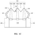
- FIG. 1C is a schematic cross-sectional view of the semiconductor device viewed along line CL 2 -CL 2 ′ in FIG. 1A .
- FIG. 2 is a flow chart showing a method for fabricating a semiconductor device in accordance with some embodiments of the present disclosure.
- FIG. 3A to FIG. 3K are schematic three-dimensional diagrams and cross-sectional views of intermediate stages showing a method for fabricating a semiconductor device in accordance with some embodiments of the present disclosure.
- FIG. 3L is a schematic cross-sectional view of a semiconductor device connected with a metal landing in accordance with some embodiments of the present disclosure.
- FIG. 4A is a schematic three-dimensional diagram showing a semiconductor device in accordance with some embodiments of the present disclosure.
- FIG. 4B is a schematic cross-sectional views of the semiconductor device viewed along line CL 4 -CL 4 ′ in FIG. 4A .
- FIG. 5 is a flow chart showing a method for fabricating a semiconductor device in accordance with some embodiments of the present disclosure.
- FIG. 6A to FIG. 6C are schematic cross-sectional views of intermediate stages showing a method for fabricating a semiconductor device in accordance with some embodiments of the present disclosure.
- FIG. 6D is a schematic cross-sectional view of a semiconductor device connected with a metal landing in accordance with some embodiments of the present disclosure.
- FIG. 7A is a schematic three-dimensional diagram showing a semiconductor device in accordance with some embodiments of the present disclosure.
- FIG. 7B is a schematic cross-sectional view of the semiconductor device viewed along line CL 7 -CL 7 ′ in FIG. 7A .
- FIG. 8 is a flow chart showing a method for fabricating a semiconductor device in accordance with some embodiments of the present disclosure.
- FIG. 9A to FIG. 9C are schematic cross-sectional views of intermediate stages showing a method for fabricating a semiconductor device in accordance with some embodiments of the present disclosure.
- FIG. 9D is a schematic cross-sectional view of a semiconductor device connected with a metal landing in accordance with some embodiments of the present disclosure.
- first and second features are formed in direct contact
- additional features may be formed between the first and second features, such that the first and second features may not be in direct contact
- the term “one” or “the” of the single form may also represent the plural form.
- the terms such as “first” and “second” are used for describing various devices, areas and layers, etc., though such terms are only used for distinguishing one device, one area or one layer from another device, another area or another layer. Therefore, the first area can also be referred to as the second area without departing from the spirit of the claimed subject matter, and the others are deduced by analogy.
- the present disclosure may repeat reference numerals and/or letters in the various examples. This repetition is for the purpose of simplicity and clarity and does not in itself dictate a relationship between the various embodiments and/or configurations discussed.
- the term “and/or” includes any and all combinations of one or more of the associated listed items.
- Embodiments of the present disclosure are directed to a fin-like field-effect transistor (FinFET) device.
- the FinFET device includes a semiconductor substrate, plural semiconductor fins on the semiconductor substrate, a source/drain structure which is located on the semiconductor substrate and connected to the semiconductor fins.
- the semiconductor fins are spaced apart from each other, and the source/drain structure has a top portion with a W-shape cross section for forming a contact landing region. With the W-shaped cross section, a contact area between the source/drain structure and a metal landing can be increased, and a contact area between a spacer of a gate structure and the source/drain structure can be decreased.
- the FinFET device includes capping layers located in recessed portions of the top portion, thereby reducing Schottky barrier height (SBH) and resistance between the source/drain structures and the metal landing.
- SBH Schottky barrier height
- FIG. 1A is a schematic three-dimensional diagram showing a semiconductor device 100 in accordance with some embodiments of the present disclosure
- FIG. 1B is a cross-sectional view of the semiconductor device 100 viewed along line CL 1 -CL 1 ′ in FIG. 1A
- FIG. 1C is a schematic cross-sectional view of the semiconductor device 100 viewed along line CL 2 -CL 2 ′ in FIG. 1A
- the semiconductor device 100 includes a semiconductor substrate 110 , plural fins 120 (shown in FIG. 1B ), source/drain structures 130 , capping layers CP, gate structures 140 , isolation structures 150 and isolation structures 160 (as shown in FIG. 1B ).
- the substrate 110 may be a semiconductor material and may include structures including a graded layer or a buried oxide, for example.
- the substrate 110 includes bulk silicon that may be undoped or doped (e.g., p-type, n-type, or a combination thereof). Other materials that are suitable for semiconductor device formation may be used. Other materials, such as germanium, quartz, sapphire, and glass could alternatively be used for the substrate 110 .
- the silicon substrate 110 may be an active layer of a semiconductor-on-insulator (SOI) substrate or a multi-layered structure such as a silicon-germanium layer formed on a bulk silicon layer.
- SOI semiconductor-on-insulator
- the isolation structures 150 are formed in the semiconductor substrate 110 .
- the isolation structures 150 act as a shallow trench isolation (STI) and may be formed by chemical vapor deposition (CVD) techniques using tetra-ethyl-ortho-silicate (TEOS) and oxygen as a precursor.
- TEOS tetra-ethyl-ortho-silicate
- the isolation structures 150 may be formed by implanting ions, such as oxygen, nitrogen, carbon, or the like, into the semiconductor substrate 110 .
- the isolation structures 150 are insulator layers of a SOI wafer.
- the fins 120 , the source/drain structures 130 and the gate structures 140 are formed on the semiconductor substrate 110 .
- the fins 120 connect the source/drain structures 130 , and are enclosed by the source/drain structures 130 and the gate structures 140 .
- Each of the gate structures 140 includes a gate electrode stack 142 and two spacers 144 , and the spacers 144 are located on sidewalls of the gate electrode stack 142 .
- the gate electrode stack 142 includes a gate electrode layer 142 a and a gate dielectric layer 142 b , but embodiments of the present disclosure are not limited thereto.
- the fins 120 protrude from the semiconductor substrate 110 .
- the gate electrode layer 142 a and the gate dielectric layer 142 b of the gate electrode stack 142 are formed on the top surfaces and sidewalls of the fins 120 .
- the isolation structures 160 (also referred to as intra-device isolation structures 160 ), such as STI structures, are formed between the fins 120 , while the intra-device isolation structures 160 are formed to space one FinFET apart from each other.
- the fins 120 are formed from the semiconductor substrate 110 .
- the fins 120 are formed from silicon germanium.
- the embodiments of the present disclosure are not limited thereto.
- the capping layers CP are formed on sidewalls of each of the source/drain structures 130 , in which structures enclosed by dotted lines represent the fins 120 .
- a thickness of each of the capping layers CP is in a range substantially from 2 nm to 10 nm, but the embodiments of the present disclosure are not limited thereto.
- the capping layers CP include a low concentration III-V semiconductor, and are lightly impurity-doped, and the source/drain structures 130 include a high concentration III-V semiconductor and are heavily impurity-doped.
- the capping layers CP include silicon germanium with a low germanium concentration, and are lightly boron-doped, and the source/drain structures 130 include silicon germanium with a high germanium concentration, and are heavily boron-doped.
- the embodiments of the present disclosure are not limited thereto.
- Each of the source/drain structures 130 has a top portion 132 with a wavy cross section, such as a W-shape cross section.
- the top portion 132 has protrusive portions 132 a and recessed portions 132 b located between every two protrusive portions 132 a .
- the protrusive portions 132 a are corresponding to the fins 120 in a one-to-one manner.
- heights of the protrusive portions 132 a are greater than or equal to heights of the fins 120 for connecting the protrusive portions 132 a with the fins 120 .
- a sidewall IS is inclined at an angle ⁇ relative to horizontal, the angle ⁇ is in a range from about 30 degrees to about 65 degrees.
- embodiments of the present disclosure are not limited thereto.
- FIG. 2 is a flow chart showing a method 200 for fabricating the semiconductor device 100 in accordance with some embodiments of the present disclosure
- FIG. 3A to FIG. 3K are schematic three-dimensional diagrams and cross-sectional views of intermediate stages showing the method 200 for fabricating the semiconductor device in accordance with some embodiments of the present disclosure.
- operation 210 is performed to provide the semiconductor substrate 110 with trenches 112 formed therein, as shown in FIG. 3A .
- the trenches 112 may be formed by using a masking layer (not shown) along with a suitable etching process.
- the masking layer may be a hardmask including silicon nitride formed through a process such as chemical vapor deposition (CVD), although other materials, such as oxides, oxynitrides, silicon carbide, combinations of these, or the like, and other processes, such as plasma enhanced chemical vapor deposition (PECVD), low pressure chemical vapor deposition (LPCVD), or even silicon oxide formation followed by nitridation, may alternatively be utilized.
- CVD chemical vapor deposition
- PECVD plasma enhanced chemical vapor deposition
- LPCVD low pressure chemical vapor deposition
- silicon oxide formation followed by nitridation may alternatively be utilized.
- the masking layer may be patterned through a suitable photolithographic process to expose those portions of the substrate 110 that will be removed to form the trenches 112 .
- operation 220 is performed to form the fins 120 along with trenches 122 , as shown in FIG. 3B .
- the second trenches 122 are located between the trenches 112 , and are intended to be intra-Fin isolation regions, such as isolation regions between separate fins 120 that share either a similar gate or similar sources or drains.
- the trenches 122 may be formed by using a similar process as the trenches 112 , such as a suitable masking or photolithography process followed by an etching process. Additionally, the formation of the trenches 122 may also be used to deepen the trenches 112 , such that the trenches 112 extend into the substrate 110 a further distance than the trenches 122 .
- operation 230 is performed to fill the trenches 112 and trenches 122 with a dielectric material to form the isolation structures 150 and the intra-device isolation structures 160 , as shown in FIG. 3C .
- the isolation structures 150 are located in the trenches 112
- the isolation structures 160 are located in the trenches 122 .
- the dielectric material used to form the isolation structures 150 and 160 may be an oxide material, a high-density plasma (HDP) oxide, or the like.
- the isolation structures 150 and 160 may be formed, after an optional cleaning and lining of the trenches 112 and 122 , using either a chemical vapor deposition (CVD) method (e.g., the HARP process), a high density plasma CVD method, or other suitable method of formation as is known in the art.
- CVD chemical vapor deposition
- HARP high density plasma CVD
- operation 240 is performed to form the gate structures 140 including the gate electrode stack 142 and the spacer 144 on the fins 120 , as shown in FIG. 3D .
- the gate dielectric layer 142 b of the gate electrode stack 142 (as shown in FIG. 1B ) may be formed by thermal oxidation, chemical vapor deposition, sputtering, or any other methods known and used in the art for forming a gate dielectric.
- the gate dielectric layer 142 b of the gate electrode stack 142 may be formed from a high permittivity (high-k) material (e.g., with a relative permittivity greater than about 5) such as lanthanum oxide, aluminum oxide, hafnium oxide, hafnium oxynitride, or zirconium oxide, or combinations thereof. Additionally, any combination of silicon dioxide, silicon oxynitride, and/or high-k materials may also be used for the gate dielectric layer 142 b.
- high-k high permittivity
- the gate electrode layer 142 a of the gate electrode stack 142 may be formed from a conductive material and may be selected from a group comprising of polycrystalline-silicon (poly-Si), poly-crystalline silicon-germanium (poly-SiGe), metallic nitrides, metallic silicides, metallic oxides, metals, combinations of these, and the like.
- metallic nitrides include tungsten nitride, molybdenum nitride, titanium nitride, and tantalum nitride, or their combinations.
- Examples of metallic silicide include tungsten silicide, titanium silicide, cobalt silicide, nickel silicide, platinum silicide, erbium silicide, or their combinations.
- Examples of metallic oxides include ruthenium oxide, indium tin oxide, or their combinations.
- Examples of metal include tungsten, titanium, aluminum, copper, molybdenum, nickel, platinum, etc.
- the gate electrode layer 142 a may be deposited by chemical vapor deposition (CVD), sputter deposition, or other techniques known and used in the art for depositing conductive materials.
- the spacers 144 may be formed from a dielectric material, such as silicon nitride, silicon carbide, silicon oxynitride, other suitable materials, and/or combinations, but embodiments of the present disclosure are not limited thereto.
- the spacers 144 may be formed by methods utilized to form such a layer, such as chemical vapor deposition (CVD), plasma enhanced CVD, sputter, and other methods known in the art.
- the top surface of the gate electrode layer 142 a may have a non-planar top surface, and may be planarized prior to patterning of the gate electrode layer 142 a . Ions may or may not be introduced into the gate electrode layer 142 a at this point. Ions may be introduced, for example, by ion implantation techniques.
- the gate electrode layer 142 a and the gate dielectric layer 142 b may be patterned to form a series of gate electrode stacks 142 over the fins 120 .
- the gate electrode stacks 142 define multiple channel regions located in the fins 120 underneath the gate dielectric layer 142 b .
- the gate electrode stack 142 may be formed by using, for example, deposition and photolithography techniques known in the art.
- a gate mask may incorporate commonly used masking materials, such as photoresist material, silicon oxide, silicon oxynitride, and/or silicon nitride, but the embodiments of the present disclosure are not limited thereto.
- the gate electrode layer 142 a and the gate dielectric layer 142 b may be etched using a dry etching process to form the patterned gate electrode stack 142 .
- the spacers 144 are formed.
- the spacers 144 may be formed on opposing sides of the gate electrode stacks 142 .
- the spacers 144 are typically formed by blanket depositing a spacer layer (not shown) on the previously formed structure.
- the spacer layer may include SiN, oxynitride, SiC, SiON, oxide, and the like and may be formed by methods utilized to form such a layer, such as chemical vapor deposition (CVD), plasma enhanced CVD, sputter, and other methods known in the art.
- the spacer layer may include a different material with different etch characteristics than the dielectric material forming the isolation structures 150 and 160 so that the spacers 144 may be used as masks for forming the isolation structures 150 and 160 (described below with references to FIG. 3E ).
- the spacers 144 may then be patterned, such as by one or more etchings operations to remove the spacer layer from the horizontal surfaces of the structure.
- operation 250 is performed to remove portions of the fins 120 from those areas not covered by the gate structures 140 , as shown in FIG. 3E .
- portions of the isolation structures 150 are removed to deduce the height of the isolation structures 150
- portions of the isolation structures 160 are removed from those areas not protected by the gate structures 140 , thereby forming exposed substrate areas for source/drain structures.
- operation 250 may be performed by a reactive ion etch (RIE) by using the gate structures 140 as hardmasks, or by any other suitable removal process.
- RIE reactive ion etch
- operation 260 is performed to form the source/drain structures 130 on the exposed substrate areas and enable the source/drain structures 130 to be connected to the fins 120 , such as shown in FIG. 3F and FIG. 3G , in which FIG. 3G is a schematic cross-sectional view of the semiconductor device viewed along line CL 3 F-CL 3 F′ in FIG. 3F .
- each one of the source/drain structures 130 is epitaxially grown from a surface of semiconductor substrate 110 in accordance with a crystal direction ⁇ 111> or ⁇ 311> to form the top portion 132 with a W-shape cross section.
- the embodiments of the present disclosure are not limited thereto.
- operation 270 is performed to form capping layers OCP to cover the entire source/drain structures 130 , as shown in FIG. 3H and FIG. 3I , in which FIG. 3I is a schematic cross-sectional view of the semiconductor device viewed along line CL 3 H-CL 3 H′ in FIG. 3H .
- the capping layers OCP are used to protect the source/drain structures 130 in subsequent operations.
- operation 280 is performed to etch portions of the capping layers OCP to expose the top portion 132 of each of the source/drain structures 130 , and portions of the capping layers CP on the sidewalls of each of the source/drain structures 130 are formed accordingly, as shown in FIG. 3J and FIG. 3K , in which FIG. 3K is a schematic cross-sectional view of the semiconductor device viewed along line CL 3 J-CL 3 J′ in FIG. 3J .
- the exposed top portion 132 is used to provide a contact landing structure. Since the top portion 132 has a W-shape cross section, a contact area between a metal landing MD and the source/drain structure 130 is increased as shown in FIG. 3L , and resistance between the metal landing MD and the source/drain structure 130 is decreased accordingly. Further, since the source/drain structure 130 has the recessed portions 132 b , a contact area between the spacer 144 of the gate structure 140 and the source/drain structure 130 is decreased, thereby improving a dislocation defect induced by the spacer 144 .
- FIG. 4A is a schematic three-dimensional diagram showing a semiconductor device 400 in accordance with some embodiments of the present disclosure
- FIG. 4B is a schematic cross-sectional views of the semiconductor device 400 viewed along line CL 4 -CL 4 ′ in FIG. 4A
- the semiconductor device 400 is similar to the semiconductor device 100 , but the difference is in that the semiconductor device 400 further includes capping layers FRCP located on the surfaces of the source/drain structures 130 .
- the capping layers FRCP are located in the recessed portions 132 b of the top portion 132 of each of the source/drain structures 130 for forming a contact landing structure as shown in FIG. 4B .
- Material of the capping layers FRCP is similar to that of the capping layers CP.
- the capping layers FRCP include silicon germanium with a low germanium concentration, and are lightly boron-doped.
- FIG. 5 is a flow chart showing a method 500 for fabricating the semiconductor device 400 in accordance with some embodiments of the present disclosure
- FIG. 6A to FIG. 6C are schematic cross-sectional views of intermediate stages showing a method for fabricating the semiconductor device in accordance with some embodiments of the present disclosure.
- operation 210 is performed to provide the semiconductor substrate 110 with trenches 112 formed therein, as shown in FIG. 3A .
- operation 220 is performed to form the fins 120 along with trenches 122 , as shown in FIG. 3B .
- operation 230 is performed to fill the trenches 112 and trenches 122 with a dielectric material to form the isolation structures 150 and the intra-device isolation structures 160 , as shown in FIG. 3C .
- operation 240 is performed to form the gate structures 140 including the gate electrode stack 142 and the spacer 144 on the fins 120 , as shown in FIG. 3D .
- operation 250 is performed to remove portions of the fins 120 from those areas not covered by the gate structures 140 , as shown in FIG. 3E . Details of the operations 210 - 250 are described above, and thus are not described again herein.
- operation 560 is performed to form the source/drain structures 130 and enable the source/drain structures 130 to be connected to the fins 120 , such as shown in FIG. 6A .
- the source/drain structures 130 are epitaxially grown from a surface of semiconductor substrate 110 in accordance with a crystal direction ⁇ 111> to form the top portion 132 with a W-shape cross section.
- operation 570 is performed to form flat capping layers FOCP on the source/drain structures 130 to cover the source/drain structures 130 , as shown in FIG. 6B .
- the flat capping layers FOCP cover the source/drain structures 130 and form flat top surfaces on the top portions 132 of the source/drain structures 130 to protect the source/drain structures 130 in subsequent operations.
- operation 580 is performed to etch the capping layers FOCP to expose the top portions 132 of the source/drain structures 130 .
- portions of the capping layers FOCP on the protrusive portions 132 a are removed, but portions of the capping layers FOCP in the recessed portions 132 b are slightly etched and remain, as shown in FIG. 6C . Therefore, the capping layers CP on the sidewalls of the source/drain structures 130 and the capping layers FRCP remaining in the recessed portions 132 b of the source/drain structures 130 are formed accordingly.
- the exposed top portion 132 is used to provide a contact landing structure, such as shown in FIG. 6D .
- the semiconductor device 400 not only includes the source/drain structure 130 having the W-shape top portion 132 , but also includes the capping layers FRCP in the recessed portions 132 b of the source/drain structure 130 .
- the capping layers FRCP in the recessed portions 132 b can reduce Schottky barrier height (SBH) and resistance between the source/drain structures 130 and the metal landing MD.
- FIG. 7A is a schematic three-dimensional diagram showing a semiconductor device 700 in accordance with some embodiments of the present disclosure
- FIG. 7B is a schematic a cross-sectional views of the semiconductor device 700 along a cut line CL 7 -CL 7 ′ in FIG. 7A
- the semiconductor device 700 is similar to the semiconductor device 100 , but the difference is in that the semiconductor device 700 further includes capping layers CRCP located on the surface of the source/drain structures 130 .
- the capping layers CRCP are located in the recessed portions 132 b of the top portion 132 of the source/drain structures 130 for forming a contact landing region as shown in FIG. 7B .
- Material of the capping layers CRCP is similar to that of the capping layers CP.
- the capping layers CRCP include silicon germanium with a low germanium concentration, and are lightly boron-doped.
- FIG. 8 is a flow chart showing a method 800 for fabricating the semiconductor device 700 in accordance with some embodiments of the present disclosure
- FIG. 9A to FIG. 9C are schematic cross-sectional views of intermediate stages showing a method for fabricating the semiconductor device in accordance with some embodiments of the present disclosure.
- operation 210 is performed to provide the semiconductor substrate 110 with trenches 112 formed therein, as shown in FIG. 3A .
- operation 220 is performed to form the fins 120 along with trenches 122 , as shown in FIG. 3B .
- operation 230 is performed to fill the trenches 112 and trenches 122 with a dielectric material to form the isolation structures 150 and the intra-device isolation structures 160 , as shown in FIG. 3C .
- operation 240 is performed to form the gate structures 140 including the gate electrode stack 142 and the spacer 144 on the fins 120 , as shown in FIG. 3D .
- operation 250 is performed to remove portions of the fins 120 from those areas not covered by the gate structures 140 , as shown in FIG. 3E . Details of the operations 210 - 250 are described above, and thus are not described again herein.
- operation 860 is performed to form the source/drain structures 130 and enable the source/drain structures 130 to be connected to the fins 120 , as shown in FIG. 9A .
- the source/drain structures 130 are epitaxially grown from a surface of semiconductor substrate 110 in accordance with a crystal direction ⁇ 111> or ⁇ 311> to form the top portion 132 with a W-shape cross section.
- operation 870 is performed to form capping layers COCP on the source/drain structures 130 to cover the source/drain structures 130 , as shown in FIG. 9B .
- the capping layers COCP are conformal to the source/drain structures 130 and cover the source/drain structures 130 to protect the source/drain structures 130 in subsequent operations. Then, operation 880 is performed to etch the capping layers COCP to expose the top portions 132 of the source/drain structures 130 . In operation 880 , portions of the capping layers COCP on the protrusive portions 132 a are removed, but portions of the capping layers COCP in the recessed portions 132 b are slightly etched and remain, as shown in FIG. 9C . Therefore, the capping layers CP on the sidewalls of the source/drain structures 130 and the capping layers CRCP remaining in the recessed portions 132 b of the source/drain structures 130 are formed accordingly.
- the exposed top portion 132 is used to provide a contact landing region, such as shown in FIG. 9D .
- the semiconductor device 700 includes the capping layers CRCP with V-shapes.
- the capping layers CRCP with V-shapes can increase a contact area between the capping layers CRCP and the metal landing MD, thereby reducing Schottky barrier height (SBH) and resistance between the source/drain structures 130 and the metal landing MD in advance.
- SBH Schottky barrier height
- a semiconductor device includes a plurality of semiconductor fins, an epitaxy structure, a capping layer, and a contact.
- the epitaxy structure adjoins the semiconductor fins.
- the epitaxy structure has a plurality of protrusive portions.
- the capping layer is over a sidewall of the epitaxy structure.
- the contact is in contact with the epitaxy structure and the capping layer.
- the contact has a portion between the protrusive portions. The portion of the contact between the protrusive portions has a bottom in contact with the epitaxy structure.
- a semiconductor device includes a plurality of semiconductor fins, an epitaxy structure, a capping layer, and a contact.
- the epitaxy structure adjoins the semiconductor fins.
- the epitaxy structure has a W-shape cross section.
- the capping layer is conformal to a sidewall of the epitaxy structure.
- the capping layer is made of a semiconductor material. The contact is in contact with the epitaxy structure and the capping layer.
- a method includes etching a semiconductor substrate to form a plurality of semiconductor fins.
- the semiconductor fins are etched to form a recess.
- the epitaxy structure is grown in the recess.
- the epitaxy structure has a W-shape cross section.
- the capping layer is formed over the epitaxy structure.
- the capping layer is at least conformal to a sidewall of the epitaxy structure.
- the capping layer is etched to expose a top surface of the epitaxy structure. A first portion of the capping layer remains over the sidewall of the epitaxy structure after etching the capping layer.
- a contact is formed and is in contact with the exposed top surface of the epitaxy structure and the first portion of the capping layer.
Abstract
Description
Claims (20)
Priority Applications (3)
| Application Number | Priority Date | Filing Date | Title |
|---|---|---|---|
| US16/160,900 US10749013B2 (en) | 2015-09-10 | 2018-10-15 | Semiconductor device and method for fabricating the same |
| US16/994,531 US11430878B2 (en) | 2015-09-10 | 2020-08-14 | Method for fabricating semiconductor device |
| US17/873,982 US11948999B2 (en) | 2015-09-10 | 2022-07-26 | Semiconductor device |
Applications Claiming Priority (2)
| Application Number | Priority Date | Filing Date | Title |
|---|---|---|---|
| US14/850,726 US10103249B2 (en) | 2015-09-10 | 2015-09-10 | FinFET device and method for fabricating the same |
| US16/160,900 US10749013B2 (en) | 2015-09-10 | 2018-10-15 | Semiconductor device and method for fabricating the same |
Related Parent Applications (1)
| Application Number | Title | Priority Date | Filing Date |
|---|---|---|---|
| US14/850,726 Continuation US10103249B2 (en) | 2015-09-10 | 2015-09-10 | FinFET device and method for fabricating the same |
Related Child Applications (1)
| Application Number | Title | Priority Date | Filing Date |
|---|---|---|---|
| US16/994,531 Division US11430878B2 (en) | 2015-09-10 | 2020-08-14 | Method for fabricating semiconductor device |
Publications (2)
| Publication Number | Publication Date |
|---|---|
| US20190051737A1 US20190051737A1 (en) | 2019-02-14 |
| US10749013B2 true US10749013B2 (en) | 2020-08-18 |
Family
ID=58257580
Family Applications (4)
| Application Number | Title | Priority Date | Filing Date |
|---|---|---|---|
| US14/850,726 Active US10103249B2 (en) | 2015-09-10 | 2015-09-10 | FinFET device and method for fabricating the same |
| US16/160,900 Active US10749013B2 (en) | 2015-09-10 | 2018-10-15 | Semiconductor device and method for fabricating the same |
| US16/994,531 Active 2036-03-23 US11430878B2 (en) | 2015-09-10 | 2020-08-14 | Method for fabricating semiconductor device |
| US17/873,982 Active US11948999B2 (en) | 2015-09-10 | 2022-07-26 | Semiconductor device |
Family Applications Before (1)
| Application Number | Title | Priority Date | Filing Date |
|---|---|---|---|
| US14/850,726 Active US10103249B2 (en) | 2015-09-10 | 2015-09-10 | FinFET device and method for fabricating the same |
Family Applications After (2)
| Application Number | Title | Priority Date | Filing Date |
|---|---|---|---|
| US16/994,531 Active 2036-03-23 US11430878B2 (en) | 2015-09-10 | 2020-08-14 | Method for fabricating semiconductor device |
| US17/873,982 Active US11948999B2 (en) | 2015-09-10 | 2022-07-26 | Semiconductor device |
Country Status (3)
| Country | Link |
|---|---|
| US (4) | US10103249B2 (en) |
| CN (2) | CN106531804A (en) |
| TW (1) | TWI685111B (en) |
Families Citing this family (10)
| Publication number | Priority date | Publication date | Assignee | Title |
|---|---|---|---|---|
| US9391201B2 (en) * | 2014-11-25 | 2016-07-12 | Taiwan Semiconductor Manufacturing Company, Ltd. | Source/drain structure and manufacturing the same |
| TWI683395B (en) * | 2015-11-12 | 2020-01-21 | 聯華電子股份有限公司 | Finfet and method of fabricating the same |
| CN109196652A (en) * | 2016-07-02 | 2019-01-11 | 英特尔公司 | Iii-v FINFET transistor with the V-shaped groove S/D profile for improved access resistance |
| US9953875B1 (en) * | 2016-11-30 | 2018-04-24 | Taiwan Semiconductor Manufacturing Company | Contact resistance control in epitaxial structures of finFET |
| US10510875B2 (en) * | 2017-07-31 | 2019-12-17 | Taiwan Semiconductor Manufacturing Co., Ltd. | Source and drain structure with reduced contact resistance and enhanced mobility |
| KR102432467B1 (en) * | 2017-08-30 | 2022-08-12 | 삼성전자주식회사 | Semiconductor device and method for fabricating the same |
| US10522680B2 (en) | 2017-08-31 | 2019-12-31 | Taiwan Semiconductor Manufacturing Co., Ltd. | Finfet semiconductor device structure with capped source drain structures |
| US11075123B2 (en) * | 2019-09-16 | 2021-07-27 | Taiwan Semiconductor Manufacturing Co., Ltd. | Method for forming isolation structure having improved gap-fill capability |
| US11728415B2 (en) * | 2020-03-27 | 2023-08-15 | Nexgen Power Systems, Inc. | Method for regrown source contacts for vertical gallium nitride based FETS |
| US11862508B2 (en) * | 2020-08-12 | 2024-01-02 | Taiwan Semiconductor Manufacturing Co., Ltd. | FinFET device and method of forming same |
Citations (18)
| Publication number | Priority date | Publication date | Assignee | Title |
|---|---|---|---|---|
| US20120049294A1 (en) | 2010-07-26 | 2012-03-01 | Taiwan Semiconductor Manufacturing Company, Ltd. | Forming Crown Active Regions for FinFETs |
| US20130277752A1 (en) | 2011-12-20 | 2013-10-24 | Glenn A. Glass | Self-aligned contact metallization for reduced contact resistance |
| US20140203370A1 (en) * | 2013-01-24 | 2014-07-24 | Shigenobu Maeda | Semiconductor Device and Fabricating Method Thereof |
| US20140217517A1 (en) | 2013-02-05 | 2014-08-07 | International Business Machines Corporation | Integrated circuits including finfet devices with lower contact resistance and reduced parasitic capacitance and methods for fabricating the same |
| US20150035023A1 (en) * | 2013-08-01 | 2015-02-05 | Seok-Hoon Kim | Semiconductor device and method for fabricating the same |
| US20150137181A1 (en) | 2013-11-19 | 2015-05-21 | International Business Machines Corporation | Stress inducing contact metal in finfet cmos |
| US20150200291A1 (en) | 2014-01-14 | 2015-07-16 | International Business Machines Corporation | Fin end spacer for preventing merger of raised active regions |
| US20150214051A1 (en) * | 2014-01-28 | 2015-07-30 | Samsung Electronics Co., Ltd. | Semiconductor devices and methods of manufacturing the same |
| US20150255567A1 (en) | 2014-03-05 | 2015-09-10 | International Business Machines Corporation | Fabrication process for mitigating external resistance of a multigate device |
| US20150333061A1 (en) * | 2014-05-13 | 2015-11-19 | Seok-Hoon Kim | Semiconductor devices having bridge layer and methods of manufacturing the same |
| US20160027918A1 (en) * | 2014-07-22 | 2016-01-28 | Nam Kyu Kim | Semiconductor device |
| US20160086950A1 (en) * | 2014-09-23 | 2016-03-24 | Dail EOM | Semiconductor device having contact plug and method of forming the same |
| US20160172357A1 (en) * | 2014-12-15 | 2016-06-16 | Hyun-Seung Song | Semiconductor device and method of fabricating the same |
| US9397099B1 (en) * | 2015-01-29 | 2016-07-19 | Taiwan Semiconductor Manufacturing Co., Ltd. | Semiconductor device having a plurality of fins and method for fabricating the same |
| US20160260669A1 (en) | 2015-03-02 | 2016-09-08 | Sun Hom PAAK | Finfets having step sided contact plugs and methods of manufacturing the same |
| US20170054003A1 (en) * | 2014-03-27 | 2017-02-23 | Intel Corporation | Confined Epitaxial Regions for Semiconductor Devices and Methods of Fabricating Semiconductor Devices Having Confined Epitaxial Regions |
| US9627481B2 (en) * | 2015-06-01 | 2017-04-18 | Samsung Electronics Co., Ltd. | Semiconductor device having an inactive-fin |
| US20190326419A1 (en) * | 2015-05-15 | 2019-10-24 | Taiwan Semiconductor Manufacturing Co., Ltd. | Semiconductor device and manufacturing method thereof |
Family Cites Families (11)
| Publication number | Priority date | Publication date | Assignee | Title |
|---|---|---|---|---|
| US7998881B1 (en) * | 2008-06-06 | 2011-08-16 | Novellus Systems, Inc. | Method for making high stress boron-doped carbon films |
| US8362568B2 (en) * | 2009-08-28 | 2013-01-29 | International Business Machines Corporation | Recessed contact for multi-gate FET optimizing series resistance |
| US8362574B2 (en) * | 2010-06-04 | 2013-01-29 | Kabushiki Kaisha Toshiba | Faceted EPI shape and half-wrap around silicide in S/D merged FinFET |
| US8901537B2 (en) * | 2010-12-21 | 2014-12-02 | Intel Corporation | Transistors with high concentration of boron doped germanium |
| US9397098B2 (en) * | 2012-03-08 | 2016-07-19 | Taiwan Semiconductor Manufacturing Company, Ltd. | FinFET-based ESD devices and methods for forming the same |
| CN104124174B (en) * | 2013-04-28 | 2017-02-22 | 中芯国际集成电路制造(上海)有限公司 | Semiconductor structure and forming method thereof |
| US9257537B2 (en) * | 2013-12-27 | 2016-02-09 | International Business Machines Corporation | Finfet including improved epitaxial topology |
| US9793356B2 (en) * | 2014-09-12 | 2017-10-17 | Samsung Electronics Co., Ltd. | Semiconductor device and method for fabricating the same |
| CN105826257B (en) * | 2015-01-06 | 2019-03-12 | 中芯国际集成电路制造(上海)有限公司 | Fin formula field effect transistor and forming method thereof |
| KR20160125208A (en) * | 2015-04-21 | 2016-10-31 | 삼성전자주식회사 | Semiconductor device having fin active regions and method of fabricating the same |
| US9397197B1 (en) * | 2015-09-23 | 2016-07-19 | International Business Machines Corporation | Forming wrap-around silicide contact on finFET |
-
2015
- 2015-09-10 US US14/850,726 patent/US10103249B2/en active Active
-
2016
- 2016-08-15 CN CN201610669330.9A patent/CN106531804A/en active Pending
- 2016-08-15 CN CN202310607132.XA patent/CN116682856A/en active Pending
- 2016-09-06 TW TW105128817A patent/TWI685111B/en active
-
2018
- 2018-10-15 US US16/160,900 patent/US10749013B2/en active Active
-
2020
- 2020-08-14 US US16/994,531 patent/US11430878B2/en active Active
-
2022
- 2022-07-26 US US17/873,982 patent/US11948999B2/en active Active
Patent Citations (19)
| Publication number | Priority date | Publication date | Assignee | Title |
|---|---|---|---|---|
| US20120049294A1 (en) | 2010-07-26 | 2012-03-01 | Taiwan Semiconductor Manufacturing Company, Ltd. | Forming Crown Active Regions for FinFETs |
| US20130277752A1 (en) | 2011-12-20 | 2013-10-24 | Glenn A. Glass | Self-aligned contact metallization for reduced contact resistance |
| US20140203370A1 (en) * | 2013-01-24 | 2014-07-24 | Shigenobu Maeda | Semiconductor Device and Fabricating Method Thereof |
| US20140217517A1 (en) | 2013-02-05 | 2014-08-07 | International Business Machines Corporation | Integrated circuits including finfet devices with lower contact resistance and reduced parasitic capacitance and methods for fabricating the same |
| US10388791B2 (en) * | 2013-08-01 | 2019-08-20 | Samsung Electronics Co., Ltd. | Semiconductor device with adjacent source/drain regions connected by a semiconductor bridge, and method for fabricating the same |
| US20150035023A1 (en) * | 2013-08-01 | 2015-02-05 | Seok-Hoon Kim | Semiconductor device and method for fabricating the same |
| US20150137181A1 (en) | 2013-11-19 | 2015-05-21 | International Business Machines Corporation | Stress inducing contact metal in finfet cmos |
| US20150200291A1 (en) | 2014-01-14 | 2015-07-16 | International Business Machines Corporation | Fin end spacer for preventing merger of raised active regions |
| US20150214051A1 (en) * | 2014-01-28 | 2015-07-30 | Samsung Electronics Co., Ltd. | Semiconductor devices and methods of manufacturing the same |
| US20150255567A1 (en) | 2014-03-05 | 2015-09-10 | International Business Machines Corporation | Fabrication process for mitigating external resistance of a multigate device |
| US20170054003A1 (en) * | 2014-03-27 | 2017-02-23 | Intel Corporation | Confined Epitaxial Regions for Semiconductor Devices and Methods of Fabricating Semiconductor Devices Having Confined Epitaxial Regions |
| US20150333061A1 (en) * | 2014-05-13 | 2015-11-19 | Seok-Hoon Kim | Semiconductor devices having bridge layer and methods of manufacturing the same |
| US20160027918A1 (en) * | 2014-07-22 | 2016-01-28 | Nam Kyu Kim | Semiconductor device |
| US20160086950A1 (en) * | 2014-09-23 | 2016-03-24 | Dail EOM | Semiconductor device having contact plug and method of forming the same |
| US20160172357A1 (en) * | 2014-12-15 | 2016-06-16 | Hyun-Seung Song | Semiconductor device and method of fabricating the same |
| US9397099B1 (en) * | 2015-01-29 | 2016-07-19 | Taiwan Semiconductor Manufacturing Co., Ltd. | Semiconductor device having a plurality of fins and method for fabricating the same |
| US20160260669A1 (en) | 2015-03-02 | 2016-09-08 | Sun Hom PAAK | Finfets having step sided contact plugs and methods of manufacturing the same |
| US20190326419A1 (en) * | 2015-05-15 | 2019-10-24 | Taiwan Semiconductor Manufacturing Co., Ltd. | Semiconductor device and manufacturing method thereof |
| US9627481B2 (en) * | 2015-06-01 | 2017-04-18 | Samsung Electronics Co., Ltd. | Semiconductor device having an inactive-fin |
Also Published As
| Publication number | Publication date |
|---|---|
| US11430878B2 (en) | 2022-08-30 |
| US20200381539A1 (en) | 2020-12-03 |
| US11948999B2 (en) | 2024-04-02 |
| CN106531804A (en) | 2017-03-22 |
| US20220359733A1 (en) | 2022-11-10 |
| US10103249B2 (en) | 2018-10-16 |
| US20170077228A1 (en) | 2017-03-16 |
| TWI685111B (en) | 2020-02-11 |
| US20190051737A1 (en) | 2019-02-14 |
| CN116682856A (en) | 2023-09-01 |
| TW201724517A (en) | 2017-07-01 |
Similar Documents
| Publication | Publication Date | Title |
|---|---|---|
| US11430878B2 (en) | Method for fabricating semiconductor device | |
| US10991795B2 (en) | Semiconductor device and manufacturing method thereof | |
| US10854602B2 (en) | FinFET device and method for fabricating the same | |
| US9905646B2 (en) | V-shaped epitaxially formed semiconductor layer | |
| US10490552B2 (en) | FinFET device having flat-top epitaxial features and method of making the same | |
| US9659964B2 (en) | Method and structure for preventing epi merging in embedded dynamic random access memory | |
| US20140175374A1 (en) | Hybrid cmos nanowire mesh device and finfet device | |
| US20140175375A1 (en) | Hybrid cmos nanowire mesh device and pdsoi device | |
| US20190157155A1 (en) | Structure and formation method of semiconductor device with fin structures | |
| KR20180069674A (en) | Semiconductor device having merged epitaxial features with arc-like bottom surface and method of making the same | |
| US20210313181A1 (en) | Cut metal gate refill with void | |
| US10164097B2 (en) | Semiconductor device and manufacturing method thereof | |
| US20230378181A1 (en) | Finfet device having flat-top epitaxial features and method of making the same | |
| US10755943B2 (en) | Method for manufacturing semiconductor device | |
| US20230395693A1 (en) | Semiconductor device and manufacturing method thereof | |
| US20230317791A1 (en) | Semiconductor device and manufacturing method thereof |
Legal Events
| Date | Code | Title | Description |
|---|---|---|---|
| FEPP | Fee payment procedure |
Free format text: ENTITY STATUS SET TO UNDISCOUNTED (ORIGINAL EVENT CODE: BIG.); ENTITY STATUS OF PATENT OWNER: LARGE ENTITY |
|
| AS | Assignment |
Owner name: TAIWAN SEMICONDUCTOR MANUFACTURING CO., LTD., TAIW Free format text: ASSIGNMENT OF ASSIGNORS INTEREST;ASSIGNORS:LEE, YEN-RU;LI, CHII-HORNG;KUO, CHIEN-I;AND OTHERS;SIGNING DATES FROM 20150916 TO 20150917;REEL/FRAME:047239/0506 Owner name: TAIWAN SEMICONDUCTOR MANUFACTURING CO., LTD., TAIWAN Free format text: ASSIGNMENT OF ASSIGNORS INTEREST;ASSIGNORS:LEE, YEN-RU;LI, CHII-HORNG;KUO, CHIEN-I;AND OTHERS;SIGNING DATES FROM 20150916 TO 20150917;REEL/FRAME:047239/0506 |
|
| STPP | Information on status: patent application and granting procedure in general |
Free format text: APPLICATION DISPATCHED FROM PREEXAM, NOT YET DOCKETED |
|
| STPP | Information on status: patent application and granting procedure in general |
Free format text: DOCKETED NEW CASE - READY FOR EXAMINATION |
|
| STPP | Information on status: patent application and granting procedure in general |
Free format text: NON FINAL ACTION MAILED |
|
| STPP | Information on status: patent application and granting procedure in general |
Free format text: RESPONSE TO NON-FINAL OFFICE ACTION ENTERED AND FORWARDED TO EXAMINER |
|
| STPP | Information on status: patent application and granting procedure in general |
Free format text: NON FINAL ACTION MAILED |
|
| STPP | Information on status: patent application and granting procedure in general |
Free format text: NOTICE OF ALLOWANCE MAILED -- APPLICATION RECEIVED IN OFFICE OF PUBLICATIONS |
|
| STPP | Information on status: patent application and granting procedure in general |
Free format text: PUBLICATIONS -- ISSUE FEE PAYMENT VERIFIED |
|
| STCF | Information on status: patent grant |
Free format text: PATENTED CASE |
|
| MAFP | Maintenance fee payment |
Free format text: PAYMENT OF MAINTENANCE FEE, 4TH YEAR, LARGE ENTITY (ORIGINAL EVENT CODE: M1551); ENTITY STATUS OF PATENT OWNER: LARGE ENTITY Year of fee payment: 4 |