US10741265B2 - Flash memory cell and associated decoders - Google Patents
Flash memory cell and associated decoders Download PDFInfo
- Publication number
- US10741265B2 US10741265B2 US15/924,100 US201815924100A US10741265B2 US 10741265 B2 US10741265 B2 US 10741265B2 US 201815924100 A US201815924100 A US 201815924100A US 10741265 B2 US10741265 B2 US 10741265B2
- Authority
- US
- United States
- Prior art keywords
- source line
- decoder
- flash memory
- erase gate
- voltage
- Prior art date
- Legal status (The legal status is an assumption and is not a legal conclusion. Google has not performed a legal analysis and makes no representation as to the accuracy of the status listed.)
- Active
Links
- 230000004044 response Effects 0.000 claims description 16
- 238000007667 floating Methods 0.000 description 15
- 230000008878 coupling Effects 0.000 description 13
- 238000010168 coupling process Methods 0.000 description 13
- 238000005859 coupling reaction Methods 0.000 description 13
- 238000003491 array Methods 0.000 description 9
- 238000013461 design Methods 0.000 description 9
- 230000000295 complement effect Effects 0.000 description 4
- 238000010586 diagram Methods 0.000 description 4
- 230000006870 function Effects 0.000 description 4
- 239000000758 substrate Substances 0.000 description 4
- 238000012544 monitoring process Methods 0.000 description 3
- 230000007246 mechanism Effects 0.000 description 2
- 230000005689 Fowler Nordheim tunneling Effects 0.000 description 1
- 230000003044 adaptive effect Effects 0.000 description 1
- 230000008859 change Effects 0.000 description 1
- 238000004891 communication Methods 0.000 description 1
- 238000010276 construction Methods 0.000 description 1
- 239000002784 hot electron Substances 0.000 description 1
- 238000000034 method Methods 0.000 description 1
- 239000004065 semiconductor Substances 0.000 description 1
- 238000012360 testing method Methods 0.000 description 1
Images


Classifications
-
- G—PHYSICS
- G11—INFORMATION STORAGE
- G11C—STATIC STORES
- G11C16/00—Erasable programmable read-only memories
- G11C16/02—Erasable programmable read-only memories electrically programmable
- G11C16/06—Auxiliary circuits, e.g. for writing into memory
- G11C16/34—Determination of programming status, e.g. threshold voltage, overprogramming or underprogramming, retention
- G11C16/3418—Disturbance prevention or evaluation; Refreshing of disturbed memory data
- G11C16/3431—Circuits or methods to detect disturbed nonvolatile memory cells, e.g. which still read as programmed but with threshold less than the program verify threshold or read as erased but with threshold greater than the erase verify threshold, and to reverse the disturbance via a refreshing programming or erasing step
-
- G—PHYSICS
- G11—INFORMATION STORAGE
- G11C—STATIC STORES
- G11C16/00—Erasable programmable read-only memories
- G11C16/02—Erasable programmable read-only memories electrically programmable
- G11C16/06—Auxiliary circuits, e.g. for writing into memory
- G11C16/08—Address circuits; Decoders; Word-line control circuits
-
- G—PHYSICS
- G11—INFORMATION STORAGE
- G11C—STATIC STORES
- G11C16/00—Erasable programmable read-only memories
- G11C16/02—Erasable programmable read-only memories electrically programmable
- G11C16/04—Erasable programmable read-only memories electrically programmable using variable threshold transistors, e.g. FAMOS
- G11C16/0408—Erasable programmable read-only memories electrically programmable using variable threshold transistors, e.g. FAMOS comprising cells containing floating gate transistors
- G11C16/0425—Erasable programmable read-only memories electrically programmable using variable threshold transistors, e.g. FAMOS comprising cells containing floating gate transistors comprising cells containing a merged floating gate and select transistor
-
- G—PHYSICS
- G11—INFORMATION STORAGE
- G11C—STATIC STORES
- G11C16/00—Erasable programmable read-only memories
- G11C16/02—Erasable programmable read-only memories electrically programmable
- G11C16/06—Auxiliary circuits, e.g. for writing into memory
- G11C16/10—Programming or data input circuits
- G11C16/14—Circuits for erasing electrically, e.g. erase voltage switching circuits
- G11C16/16—Circuits for erasing electrically, e.g. erase voltage switching circuits for erasing blocks, e.g. arrays, words, groups
-
- G—PHYSICS
- G11—INFORMATION STORAGE
- G11C—STATIC STORES
- G11C16/00—Erasable programmable read-only memories
- G11C16/02—Erasable programmable read-only memories electrically programmable
- G11C16/06—Auxiliary circuits, e.g. for writing into memory
- G11C16/26—Sensing or reading circuits; Data output circuits
- G11C16/28—Sensing or reading circuits; Data output circuits using differential sensing or reference cells, e.g. dummy cells
-
- G—PHYSICS
- G11—INFORMATION STORAGE
- G11C—STATIC STORES
- G11C16/00—Erasable programmable read-only memories
- G11C16/02—Erasable programmable read-only memories electrically programmable
- G11C16/06—Auxiliary circuits, e.g. for writing into memory
- G11C16/30—Power supply circuits
-
- G—PHYSICS
- G11—INFORMATION STORAGE
- G11C—STATIC STORES
- G11C16/00—Erasable programmable read-only memories
- G11C16/02—Erasable programmable read-only memories electrically programmable
- G11C16/06—Auxiliary circuits, e.g. for writing into memory
- G11C16/34—Determination of programming status, e.g. threshold voltage, overprogramming or underprogramming, retention
- G11C16/3418—Disturbance prevention or evaluation; Refreshing of disturbed memory data
-
- G—PHYSICS
- G11—INFORMATION STORAGE
- G11C—STATIC STORES
- G11C7/00—Arrangements for writing information into, or reading information out from, a digital store
- G11C7/14—Dummy cell management; Sense reference voltage generators
-
- G—PHYSICS
- G11—INFORMATION STORAGE
- G11C—STATIC STORES
- G11C8/00—Arrangements for selecting an address in a digital store
- G11C8/08—Word line control circuits, e.g. drivers, boosters, pull-up circuits, pull-down circuits, precharging circuits, for word lines
-
- H—ELECTRICITY
- H01—ELECTRIC ELEMENTS
- H01L—SEMICONDUCTOR DEVICES NOT COVERED BY CLASS H10
- H01L29/00—Semiconductor devices adapted for rectifying, amplifying, oscillating or switching, or capacitors or resistors with at least one potential-jump barrier or surface barrier, e.g. PN junction depletion layer or carrier concentration layer; Details of semiconductor bodies or of electrodes thereof ; Multistep manufacturing processes therefor
- H01L29/40—Electrodes ; Multistep manufacturing processes therefor
- H01L29/41—Electrodes ; Multistep manufacturing processes therefor characterised by their shape, relative sizes or dispositions
- H01L29/423—Electrodes ; Multistep manufacturing processes therefor characterised by their shape, relative sizes or dispositions not carrying the current to be rectified, amplified or switched
- H01L29/42312—Gate electrodes for field effect devices
- H01L29/42316—Gate electrodes for field effect devices for field-effect transistors
- H01L29/4232—Gate electrodes for field effect devices for field-effect transistors with insulated gate
- H01L29/42324—Gate electrodes for transistors with a floating gate
- H01L29/42328—Gate electrodes for transistors with a floating gate with at least one additional gate other than the floating gate and the control gate, e.g. program gate, erase gate or select gate
Definitions
- the present invention relates to a flash memory cell with only four terminals and decoder circuitry for operating an array of such flash memory cells.
- the invention allows for fewer terminals for each flash memory cell compared to the prior art, which results in a simplification of the decoder circuitry and overall die space required per flash memory cells.
- the invention also provides for the use of high voltages on one or more of the four terminals to allow for read, erase, and programming operations despite the lower number of terminals compared to prior art flash memory cells.
- Non-volatile memory cells are well known in the art.
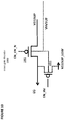
- Memory cell 10 comprises semiconductor substrate 12 of a first conductivity type, such as P type.
- Substrate 12 has a surface on which there is formed a first region 14 (also known as the source line SL) of a second conductivity type, such as N type.
- a second region 16 also of N type is formed on the surface of substrate 12 .
- Bit line BL 20 is connected to the second region 16 .
- Word line WL 22 is positioned above a first portion of the channel region 18 and is insulated therefrom.
- Word line 22 has little or no overlap with the second region 16 .
- Floating gate FG 24 is over another portion of channel region 18 .
- Floating gate 24 is insulated therefrom, and is adjacent to word line 22 .
- Floating gate 24 is also adjacent to the first region 14 .
- Floating gate 24 may overlap the first region 14 to provide coupling from the first region 14 into floating gate 24 .
- Coupling gate CG (also known as control gate) 26 is over floating gate 24 and is insulated therefrom.
- Erase gate EG 28 is over the first region 14 and is adjacent to floating gate 24 and coupling gate 26 and is insulated therefrom.
- the top corner of floating gate 24 may point toward the inside corner of the T-shaped erase gate 28 to enhance erase efficiency.
- Erase gate 28 is also insulated from the first region 14 .
- Memory cell 10 is more particularly described in U.S. Pat. No. 7,868,375, whose disclosure is incorporated herein by reference in its entirety.
- One exemplary operation for erase and program of prior art non-volatile memory cell 10 is as follows. Memory cell 10 is erased, through a Fowler-Nordheim tunneling mechanism, by applying a high voltage on erase gate 28 with other terminals equal to zero volt. Electrons tunnel from floating gate 24 into erase gate 28 causing floating gate 24 to be positively charged, turning on the cell 10 in a read condition. The resulting cell erased state is known as ‘1’ state.
- Memory cell 10 is programmed, through a source side hot electron programming mechanism, by applying a high voltage on coupling gate 26 , a high voltage on source line 14 , a medium voltage on erase gate 28 , and a programming current on bit line 20 .
- a portion of electrons flowing across the gap between word line 22 and floating gate 24 acquire enough energy to inject into floating gate 24 causing the floating gate 24 to be negatively charged, turning off the cell 10 in a read condition.
- the resulting cell programmed state is known as ‘0’ state.
- Memory cell 10 is read in a Current Sensing Mode as following: A bias voltage is applied on bit line 20 , a bias voltage is applied on word line 22 , a bias voltage is applied on coupling gate 26 , a bias or zero voltage is applied on erase gate 28 , and a ground is applied on source line 14 . There exists a cell current flowing from bit line 20 to source line 14 for an erased state and there is insignificant or zero cell current flow from the bit line 20 to the source line 14 for a programmed state.
- memory cell 10 can be read in a Reverse Current Sensing Mode, in which bit line 20 is grounded and a bias voltage is applied on source line 24 . In this mode the current reverses the direction from source line 14 to bitline 20 .
- Memory cell 10 alternatively can be read in a Voltage Sensing Mode as following: A bias current (to ground) is applied on bit line 20 , a bias voltage is applied on word line 22 , a bias voltage is applied on coupling gate 26 , a bias voltage is applied on erase gate 28 , and a bias voltage is applied on source line 14 . There exists a cell output voltage (significantly >0V) on bit line 20 for an erased state and there is insignificant or close to zero output voltage on bit line 20 for a programmed state.
- memory cell 10 can be read in a Reverse Voltage Sensing Mode, in which bit line 20 is biased at a bias voltage and a bias current (to ground) is applied on source line 14 . In this mode, memory cell 10 output voltage is on the source line 14 instead of on the bit line 20 .
- the logic circuit 270 In response to the read, erase or program command, the logic circuit 270 (in FIG. 2 ) causes the various voltages to be supplied in a timely and least disturb manner to the various portions of both the selected memory cell 10 and the unselected memory cells 10 .
- the voltage and current applied are as follows. As used hereinafter, the following abbreviations are used: source line or first region 14 (SL), bit line 20 (BL), word line 22 (WL), and coupling gate 26 (CG).
- negative voltages can be applied to word line 22 when memory cell 10 is unselected during read, erase, and program operations, and negative voltages can be applied to coupling gate 26 during an erase operation, such that the following voltages are applied:
- the CGINH signal listed above is an inhibit signal that is applied to the coupling gate 26 of an unselected cell that shares an erase gate 28 with a selected cell.
- FIG. 2 depicts an embodiment recently developed by applicant of an architecture for a flash memory system comprising die 200 .
- Die 200 comprises: memory array 215 and memory array 220 for storing data, memory arrays 215 and 220 comprising rows and columns of memory cells of the type described previously as memory cell 10 in FIG.
- pad 240 and pad 280 for enabling electrical communication between the other components of die 200 and, typically, wire bonds (not shown) that in turn connect to pins (not shown) or package bumps that are used to access the integrated circuit from outside of the packaged chip or macro interface pins (not shown) for interconnecting to other macros on a SOC (system on chip); high voltage circuit 275 used to provide positive and negative voltage supplies for the system; control logic 270 for providing various control functions, such as redundancy and built-in self-testing; analog circuit 265 ; sensing circuits 260 and 261 used to read data from memory array 215 and memory array 220 , respectively; row decoder circuit 245 and row decoder circuit 246 used to access the row in memory array 215 and memory array 220 , respectively, to be read from or written to; column decoder circuit 255 and column decoder circuit 256 used to access bytes in memory array 215 and memory array 220 , respectively, to be read from or written to; charge pump circuit 250 and charge pump circuit 25
- flash memory cell design that utilizes fewer terminals than in the prior art and simplified circuitry for operating flash memory cells that follow that design.
- the present invention relates to a flash memory cell with only four terminals and decoder circuitry for operating an array of such flash memory cells.
- the invention allows for fewer terminals for each flash memory cell compared to the prior art, which results in a simplification of the decoder circuitry and overall die space required per flash memory cells.
- the invention also provides for the use of high voltages on one or more of the four terminals to allow for read, erase, and programming operations despite the lower number of terminals compared to prior art flash memory cells.
- FIG. 1 is a cross-sectional view of a non-volatile memory cell of the prior art to which the method of the present invention can be applied.
- FIG. 2 is a block diagram of a non-volatile memory device using the non-volatile memory cell of the prior art shown in FIG. 1 .
- FIG. 3 is a block diagram of an embodiment of a non-volatile memory cell.
- FIG. 4 is a schematic representation of the non-volatile memory cell of FIG. 3 .
- FIG. 5 is a block diagram of a non-volatile memory device using the non-volatile memory cell of FIG. 3 .
- FIG. 6 depicts an embodiment of a row decoder for use with the memory device of claim 5 .
- FIG. 7 is a block diagram of decoder circuitry for use with the memory device of claim 5 .
- FIG. 8 depicts an embodiment of an erase gate decoder for use with the memory device of claim 5 .
- FIG. 9 depicts an embodiment of an erase gate decoder for use with the memory device of claim 5 .
- FIG. 10 depicts an embodiment of an erase gate decoder for use with the memory device of claim 5 .
- FIG. 11 depicts an embodiment of a source line decoder for use with the memory device of claim 5 .
- FIG. 12 depicts an embodiment of a source line decoder for use with the memory device of claim 5 .
- FIG. 13 depicts an embodiment of a source line decoder for use with the memory device of claim 5 .
- FIG. 14 depicts an embodiment of a source line decoder for use with the memory device of claim 5 .
- FIG. 15 depicts an embodiment of a source line decoder with a dummy flash memory cell for selectively pulling down to a low voltage or ground a source line.
- FIG. 16 depicts an embodiment of a dummy flash memory cell for selectively pulling down to a low voltage or ground a source line coupled to a selected flash memory cell.
- FIG. 17 depicts an embodiment of a control gate decoder for use with a memory device using the memory cell of claim 1 .
- FIG. 18 depicts an embodiment of a control gate decoder for use with a memory device using the memory cell of claim 1 .
- FIG. 19 depicts an embodiment of a gate decoder for use with a memory device using the memory cell of claim 1 .
- FIG. 20 depicts an embodiment of a latch voltage level shifter for use with the memory device of claim 5 .
- FIG. 21 depicts an embodiment of a latch voltage level shifter for use with the memory device of claim 5 .
- FIG. 22 depicts an embodiment of a high voltage current limiter for use with the memory device of claim 5 .
- FIG. 23 depicts an embodiment of a latch voltage level shifter for use with the memory device of claim 5 .
- FIG. 24 depicts an embodiment of an array of flash memory cells with a column of dummy memory cells for selectively pulling down to a low voltage or ground a selected source line.
- FIG. 3 depicts an embodiment of an improved flash memory cell 300 .
- flash memory cell 300 comprises substrate 12 , first region (source line) 14 , second region 16 , channel region 18 , bit line 20 , word line 22 , floating gate 24 , and erase gate 28 .
- flash memory cell 300 does not contain a coupling gate or control gate and only contains four terminals—bit line 20 , word line 22 , erase gate 28 , and source line 14 . This significantly reduces the complexity of the circuitry, such as decoder circuitry, required to operate an array of flash memory cells.
- the erase operation (erasing through erase gate) and read operation are similar to that of the FIG. 1 except there is no control gate bias.
- the programming operation also is done without the control gate bias, hence the program voltage on the source line is higher to compensate for lack of control gate bias.
- Table No. 4 depicts typical voltage ranges that can be applied to the four terminals for performing read, erase, and program operations:
- FIG. 4 depicts a symbolic representation 400 of flash memory cell 300 .
- Symbolic representation 400 comprises symbols for the four terminals of flash memory cell 300 , namely, bit line 20 , word line 22 , erase gate 28 , and source line 14 .
- FIG. 5 depicts an embodiment of an architecture for a flash memory system comprising die 500 .
- Die 500 comprises memory arrays 501 , 511 , 521 , and 531 , for storing data, each of memory arrays 501 , 511 , 521 , and 531 comprising rows and columns of memory cells of the type described previously as flash memory cell 300 in FIG. 3 .
- Die 500 further comprises sensing circuit 543 used to read data from memory arrays 501 , 511 , 521 , and 531 ; row decoder circuit 541 used to access the selected row in memory arrays 501 and 511 and row decoder circuit 542 used to access the selected row in memory arrays 521 and to be read from or written to; column decoder circuits 503 , 513 , 523 , and 533 used to access bytes in memory arrays 501 , 511 , 521 , and 531 , respectively, to be read from or written to; high voltage row decoder WSHDR 502 , 512 , 522 , and 532 used to provide high voltage to one or more terminals of the selected memory cell within memory arrays 501 , 511 , 521 , and 531 , respectively, depending on the operation being performed.
- sensing circuit 543 used to read data from memory arrays 501 , 511 , 521 , and 531 ;
- row decoder circuit 541 used
- Die 500 further comprises the following functional structures and sub-systems: macro interface pins ITFC pin 548 for interconnecting to other macros on a SOC (system on chip); low voltage generation (including a low voltage charge pump circuit) circuits 547 and high voltage generation (including a high voltage charge pump circuit) circuit 546 used to provide increased voltages for program and erase operations for memory arrays 501 , 511 , 521 , and 531 ; analog circuit 544 used by analog circuitry on die 500 ; digital logic circuit 545 used by digital circuitry on die 500 .
- macro interface pins ITFC pin 548 for interconnecting to other macros on a SOC (system on chip)
- analog circuit 544 used by analog circuitry on die 500
- digital logic circuit 545 used by digital
- FIG. 6 depicts row decoder 600 for 8 word lines in a sector within a memory array (such as memory array 501 , 511 , 521 , and 531 ).
- Row decoder 600 can be part of row decoder circuits 541 and 542 in die 500 .
- Row decoder 600 comprises NAND gate 601 , which receives pre-decoded address signals, here shown as lines XPA, XPB, XPC, and XPD, which select a sector within a memory array. When XPA, XPB XPC, and XPD are all “high,” then the output of NAND gate 601 will be “low” and this particular sector will be selected.
- Row decoder 600 further comprises inverter 602 , decoder circuit 610 to generate word line WL 0 , decoder circuit 620 to generate WL 7 , as well as additional decoder circuits (not shown) to generate word lines WL 1 , WL 2 , WL 3 , WL 4 , WL 5 , and WL 6 .
- Decoder circuit 610 comprises PMOS transistors 611 , 612 , and 614 and NMOS transistors 613 and 615 , configured as shown. Decoder circuit 610 receives the output of NAND gate 601 , the output of inverter 602 , and pre-decoded address signal XPZB0. When this particular sector is selected and XPZB0 is “low,” then WL 0 will be asserted. When XPZB0 is “high,” then WL 0 will not be asserted.
- decoder circuit 620 comprises PMOS transistors 621 , 622 , and 624 and NMOS transistors 623 and 625 , configured as shown. Decoder circuit 620 receives the output of NAND gate 601 , the output of inverter 602 , and pre-decoded address signal XPZ70. When this particular sector is selected and XPZB7 is “low,” then WL 7 will be asserted. When XPZB7 is “high,” then WL 7 will not be asserted.
- decoder circuits (now shown) for WL 1 , WL 2 , and WL 3 , WL 4 , WL 5 , and WL 6 will follow the same design as decoder circuits 610 and 620 except that they will receive the inputs XPZB1, XPZB2, XPZB3, XPZB4, XPZB5, and XPZB6, respectively, instead of XPZB0 or XPZB7.
- XPZB7 is “high,” signifying that WL 7 is to be not asserted, which will pull the node between PMOS transistor 622 and NMOS transistor 623 to the value of XPZB7 (which is “high”), which will turn on NMOS transistor 624 and cause WL to be “low,” which indicates a non-asserted state.
- one of the word lines WL 0 . . . WL 7 can be selected when this sector is selected.
- FIG. 7 depicts high voltage row decoder 700 . It will be recalled that in the embodiments of this invention, high voltage signals (e.g., 7-9V for the source line during a programming operation) are required to compensate for the lack of a coupling gate in the flash memory cells.
- High voltage decoder 700 comprises high voltage level shift enable circuit 710 , erase gate decoder 720 , and source line decoder 730 .
- High voltage level shift enable circuit 710 comprises high voltage level shift circuit 711 and low voltage latch 712 .
- Low voltage latch 712 receives word line (WL), enable (EN), and reset (RST) as input signals and outputs sector enable signal (SECEN) and sector enable signal bar (SECEN_N).
- Sector enable signal (SECEN) is provided as an input to high voltage level shift circuit 711 , which outputs sector enable signal high voltage (SECEN_HV 0 . . . SECEN_HVN for N sectors) and sector enable signal high voltage bar (SECEN_HV 0 _N . . . SECEN_HVN_N for N sectors).
- Erase gate decoder 720 comprises erase gate decoder 721 for row 0 in the sector, and similar erase gate decoders (not shown) for rows 1, . . . , N in the sector.
- erase gate decoder 721 receives the sector enable signal high voltage (SECEN_HV 0 ) from high voltage level shift circuit 711 , its complement (SECEN_HV 0 _N), a voltage erase gate supply (VEGSUP), a low voltage erase gate supply (VEGSUP_LOW), sector enable signal (SECEN), and its complement (SECEN_N).
- the output EG 0 of erase gate decoder 721 can be at one of three different voltage levels: SECEN_HV 0 (high voltage), VEGSUP (normal voltage), or VEGSUP_LOW (low voltage).
- source line decoder 730 comprises source line decoder 721 for row 0 in the sector, and similar source line decoders (not shown) for rows 1, . . . , N in the sector.
- source line decoder 731 receives sector enable signal high voltage (SECEN_HV 0 ) from high voltage level shift circuit 711 , its complement (SECEN_HV 0 _N), a voltage source line supply (VSLSUP), a low voltage source line supply (VSLSUP_LOW), sector enable signal (SECEN), and its complement (SECEN_N).
- SECEN_HV 0 high voltage
- VSLSUP voltage source line supply
- VSLSUP_LOW low voltage source line supply
- SECEN sector enable signal
- the output SL 0 of source line decoder 730 can be at one of three different voltage levels: SECEN_HV 0 (high voltage), VSLSUP (normal voltage), or VSLSUP_LOW (low voltage).
- FIG. 8 shows erase gate decoder 800 , which is an embodiment of erase gate decoder 720 .
- Erase gate decoder 800 comprises NMOS transistor 801 and PMOS transistors 802 and 803 , configured as shown.
- PMOS transistor 803 is a current limiter with EGHV_BIAS as a current mirror bias level.
- FIG. 9 shows erase gate decoder 900 , which another embodiment of erase gate decoder 720 .
- Erase gate decoder 900 comprises NMOS transistor 901 and PMOS transistor 902 .
- Erase gate decoder 900 in this example does not contain a current limiter.
- EN_HV_N When this erase gate signal (EG) is to be asserted, EN_HV_N will be low (e.g., 0V or 1.2V), which will turn on PMOS transistor 902 and turn off NMOS transistor 901 , which will cause erase gate (EG) to be high.
- EN_HV_N When this erase gate signal (EG) is to be not asserted, EN_HV_N will be high, which will turn off PMOS transistor 902 and turn on NMOS transistor 901 , which will cause erase gate (EG) to be low (e.g., 0V or 1.2V or 2.5V).
- FIG. 10 shows erase gate decoder 1000 , which is another embodiment of erase gate decoder 720 that uses only PMOS transistors.
- Erase gate decoder 1000 comprises PMOS transistors 1001 and 1002 , which share a common well. Erase gate decoder 1000 in this example does not contain a current limiter. When this erase gate signal (EG) is to be asserted, EN_HV_N will be low and EN_HV will be high, which will turn on PMOS transistor 1002 and turn off PMOS transistor 1001 , which will cause erase gate (EG) to be high.
- EG erase gate signal
- EN_HV_N When this erase gate signal (EG) is to be not asserted, EN_HV_N will be low and EN_HV will be high, which will turn off PMOS transistor 1002 and turn on PMOS transistor 1001 , which will cause erase gate (EG) to be low (e.g., 0V or 1.2V or 2.5V).
- FIG. 11 shows source line decoder 1100 , which is an embodiment of source line decoder 730 .
- Source line decoder 1100 comprises NMOS transistors 1101 , 1102 , 1103 , and 1104 , configured as shown.
- NMOS transistor 1101 pulls the source line (SL) low during a read operation in response to the SLRD_EN signal.
- NMOS transistor 1102 pulls the source line (SL) low during a programming operation in response to the SLP_EN signal.
- NMOS transistor 1103 performs a monitoring function, through output VSLMON.
- NMOS transistor 1104 provides a voltage to source line (SL) in response to the EN_HV signal.
- FIG. 12 shows source line decoder 1200 , which is another embodiment of source line decoder 730 .
- Source line decoder 1200 comprises NMOS transistors 1201 , 1202 , and 1203 , configured as shown.
- NMOS transistor 1201 pulls the source line (SL) low during a programming operation in response to the SLP_EN signal.
- NMOS transistor 1202 performs a monitoring function, through output VSLMON.
- NMOS transistor 1203 provides a voltage to source line (SL) in response to the EN_HV signal.
- FIG. 13 shows source line decoder 1300 , which is another embodiment of source line decoder 730 .
- Source line decoder 730 comprises NMOS transistors 1301 and 1302 , configured as shown.
- NMOS transistor 1301 pulls the source line (SL) low during a programming operation in response to the SLP_EN signal.
- NMOS transistor 1302 provides a voltage to source line (SL) in response to the EN_HV signal.
- FIG. 14 shows source line decoder 1400 , which is another embodiment of source line decoder 730 that uses only PMOS transistors.
- Source line decoder 1400 comprises PMOS transistors 1401 , 1402 , and 1403 , configured as shown.
- PMOS transistor 1401 pulls the source line (SL) low during a programming operation in response to the EN_HV signal.
- PMOS transistor 1402 performs a monitoring function, through output VSLMON.
- PMOS transistor 1403 provides a voltage to source line (SL) in response to the EN_HV_N signal.
- FIG. 15 depicts source line decoder 1500 , which is another embodiment of source line decoder 730 that is a variation of source line decoder 1400 in FIG. 14 .
- Source line decoder comprises source line decoder 1400 .
- the source line (SL) of source line decoder 1400 is connected to the source line 1620 of selected memory cell 1620 and source line 1520 of a dummy memory cell 1510 during read operations.
- Dummy memory cell 1510 follows the same construction as selected memory cell 1610 , which can be based on the design of memory cell 300 , except that dummy memory cell 1510 is not used to store data.
- FIG. 16 shows additional detail regarding selected memory cell 1620 and dummy memory cell 1520 .
- source line 1620 and source line 1520 are coupled to ground through dummy memory cell 1510 and dummy bitline 1526 which is coupled to ground.
- Dummy memory cell 1510 is required to be erased before read operation. This will pull source line 1520 and source line 1620 to ground.
- bitline 1526 When selected memory cell 1610 is in program mode, bitline 1526 is coupled to an inhibit voltage such as VDD. This will place dummy memory cell 1510 in a program inhibit mode which will maintain dummy memory cell 1520 in am erased state.
- a plurality of the dummy cells, such as dummy memory cell 1510 can be connected to memory cell 1610 through their source lines to strengthen the pull down of the source line 1620 to ground.
- FIG. 17 depicts control gate decoder 1700 , which is a control gate decoder that can be used with the prior art design of FIGS. 1-2 , and which is not needed in the embodiments of FIGS. 3-16 .
- Control gate decoder 1700 comprises NMOS transistor 1701 and PMOS transistor 1702 .
- NMOS transistor 1701 will pull down the control gate signal (CG) in response to the signal EN_HV_N.
- PMOS transistor 1702 will pull up the control gate signal (CG) in response to the signal EN_HV_N.
- FIG. 18 depicts control gate decoder 1800 that uses only PMOS transistors, which is another embodiment of a control gate decoder that can be used with the prior art design of FIGS. 1-2 , and which is not needed in the embodiments of FIGS. 3-16 .
- Control gate decoder 1800 comprises PMOS transistors 1801 and 1802 .
- PMOS transistor 1801 will pull down the control gate signal (CG) in response to the signal EN_HV.
- PMOS transistor 1802 will pull up the control gate signal (CG) in response to the signal EN_HV_N.
- FIG. 19 depicts EG/CG/SL gate decoder 1900 , that can be used with the prior art design of FIGS. 1-2 , and in the embodiments of FIGS. 3-16 , thus showing the amount of space saved through the present invention.
- Gate decoder 1900 comprises PMOS transistors 1901 .
- PMOS transistor 1901 will pull low the gate signal (EG/CG/SL) high in response to the signal EN_HV_N. If EN_HV_N is not asserted, then the value of EG/CG/SL will float.
- the EG/CG/SL gate is pre-charged to a low bias level first before being enabled to a high voltage level.
- FIG. 20 depicts latch voltage level shifter 2000 with adaptive high voltage VH and low VL supplies.
- Latch voltage level shifter comprises a latch comprising inverters 2001 and 2002 and NMOS transistors 2003 , 2004 , 2005 , 2006 , and 2007 , in the configuration shown.
- Latch voltage level shifter receives input 2012 to reset (input RST_SECDEC) and input 2010 to set, meaning enabling, (inputs WL 0 and SET_SECDEC) and produces output 2020 and 2022 .
- Latch voltage level shifter will adaptively change the magnitudes of a “high” voltage or a “low” voltage to minimize the voltage stress.
- the latch inverters 2001 and 2002 received power supply high VH and power supply low VL.
- VH is Vdd, e.g. 1.2V
- VL is gnd.
- VH starts to ramp up to an intermediate VH level, e.g. 5V.
- VL then ramps to an intermediate VL level, e.g., 2.5V.
- VH then ramps to final high voltage supply VHVSUP level, e.g., 11.5V.
- VHVSUP level e.g. 11.5V.
- FIG. 21 depicts latch voltage shifter 2100 .
- Latch voltage shifter 2100 comprises low voltage latch inverter 2109 , NMOS transistors 2103 , 2104 , 2107 , and 2108 , and PMOS transistors 2101 , 2102 , 2105 , and 2106 , in the configuration shown.
- Latch voltage shifter 2100 receives EN_SEC as an input and outputs EN_HV and EN_HV_N, which have a larger voltage swing than EN_SEC and ground.
- FIG. 22 depicts high voltage current limiter 2200 , which comprises a PMOS transistor that receives VEGSUP_LOC and outputs VEGSUP with a limited current (acting as a current bias)
- This circuit can be used with the circuits that do not have local current limiter such as in FIGS. 9,10,17,18,19 to limit current.
- FIG. 23 depicts latch voltage shifter 2300 with a current limiter for read operations.
- Latch voltage shifter 2300 comprises latch voltage shifter 2100 from FIG. 21 . It also comprises current limiter 2310 comprising PMOS transistor 2301 and current source 2302 . Current limiter 2310 is connected to current limiter 2310 through switch 2303 . Latch voltage shifter 2100 also is connected to the signal HVSUP_GLB through switch 2304 . During a read operation, latch voltage level shifter 2100 will be connected to current limiter 2310 through switch 2303 . The outputs (e.g., approximately one Vt threshold voltage below Vdd 2.5V) of the latch voltage level shifter 2100 control the gate of the EG and CG decoders as in FIGS. 8,9,10,17,18,19 . When not in a read operation, latch voltage level shifter 2100 will be connected to HVSUP_GLB through switch 2304 .
- the outputs e.g., approximately one Vt threshold voltage below Vdd 2.5V
- FIG. 24 depicts an array with source line pulldown 2400 , which utilizes the designs of FIGS. 15 and 16 .
- Array with source line pulldown 2400 comprises a plurality of memory cells organized into rows (indicated by word lines WL 0 , . . . WL 7 ) and columns (indicated by bit lines BL 0 , . . . , BL 31 ).
- An exemplary memory cell pair is memory cell pair 2401 , which comprises one cell coupled to word line 2402 (WL 0 ) and another cell coupled to word line 2404 (WL 1 ).
- the two cells share erase gate 2403 (EG 0 ) and source line 2406 (SL 0 ).
- a column of dummy memory cells also is present, here shown attached to bit line BL_PWDN 1 .
- An exemplary dummy memory cell pair is dummy memory cell pair 2407 , which comprises one cell coupled to word line 2402 (WL 0 ) and another cell coupled to word line 2404 (WL 1 ).
- the two cells share erase gate 2403 (EG 0 ) and source line 2406 (SL 0 ).
- the selected memory cells and dummy memory cells can be configured during read operations as discussed previously for FIGS. 15 and 16 .
Abstract
Description
| TABLE NO. 1 |
| PEO (Positive Erase Operation) Table |
| WL- | BL- | CG-unsel | CG- | EG- | |||||||
| WL | unsel | BL | unsel | CG | same sector | unsel | EG | unsel | SL | SL-unsel | |
| Read | 1.0-2 | V | 0 V | 0.6-2 | V | 0 V-FLT | 0-2.6 | V | 0-2.6 V | 0-2.6 V | 0-2.6 | V | 0-2.6 V | 0 | V | 0 V-FLT |
| Erase | 0 | V | 0 V | 0 | V | 0 V | 0 | V | 0-2.6 V | 0-2.6 V | 11.5-12 | V | 0-2.6 V | 0 | V | 0 V |
| Program | 1 | V | 0 V | 1 | uA | Vinh | 10-11 | V | 0-2.6 V | 0-2.6 V | 4.5-5 | V | 0-2.6 V | 4.5-5 | V | 0-1 V/FLT |
| TABLE NO. 2 |
| PEO (Positive Erase Operation) Table |
| WL- | BL- | CG-unsel | CG- | EG- | |||||||
| WL | unsel | BL | unsel | CG | same sector | unsel | EG | unsel | SL | SL-unsel | |
| Read | 1.0-2 | V | −0.5 V/0 V | 0.6-2 | V | 0 V-FLT | 0-2.6 | V | 0-2.6 V | 0-2.6 V | 0-2.6 | V | 0-2.6 V | 0 | V | 0 V-FLT |
| Erase | 0 | V | 0 V | 0 | V | 0 V | 0 | V | 0-2.6 V | 0-2.6 V | 11.5-12 | V | 0-2.6 V | 0 | V | 0 V |
| Program | 1 | V | −0.5 V/0 V | 1 | uA | Vinh | 10-11 | V | 0-2.6 V | 0-2.6 V | 4.5-5 | V | 0-2.6 V | 4.5-5 | V | 0-1 V/FLT |
| TABLE NO. 3 |
| PNEO (Positive Negative Erase Operation) Table |
| WL- | BL- | CG-unsel | CG- | EG- | |||||||
| WL | unsel | BL | unsel | CG | same sector | unsel | EG | unsel | SL | SL-unsel | |
| Read | 1.0-2 | V | −0.5 V/0 V | 0.6-2 | V | 0-FLT | 0-2.6 | V | 0-2.6 V | 0-2.6 V | 0-2.6 | V | 0-2.6 V | 0 | V | 0-FLT |
| Erase | 0 | V | −0.5 V/0 V | 0 | V | 0-FLT | −(5-9) | V | 0-2.6 V | 0-2.6 V | 8-9 | V | 0-2.6 V | 0 | V | 0 V |
| Program | 1 | V | −0.5 V/0 V | 1 | uA | Vinh | 8-9 | V | CGINH | 0-2.6 V | 8-9 | V | 0-2.6 V | 4.5-5 | V | 0-1 V/FLT |
| (4-6 V) | ||||||||||||||||
| TABLE NO. 4 |
| Four Terminal Flash Device Operation Table |
| WL- | BL- | EG- | ||||||
| WL | unsel | BL | unsel | EG | unsel | SL | SL-unsel | |
| Read | 0.7-2.2 | V | −0.5 V/0 V | 0.6-2 | V | 0 V-FLT | 0-2.6 | V | 0-2.6 V | 0 | V | 0 V/FLT/VB |
| Erase | −0.5 V/0 V | −.5 V/0 V | 0 | V | 0 V | 11.5 | V | 0-2.6 V | 0 | V | 0 V |
| Program | 1-1.5 | V | −.5 V/0 V | 1-3 | μA | Vinh | 4.5 | V | 0-2.6 V | 7-9 | V | 0-1 V/FLT |
| (~1.8 V) | ||||||||||||
Claims (10)
Priority Applications (3)
| Application Number | Priority Date | Filing Date | Title |
|---|---|---|---|
| US15/924,100 US10741265B2 (en) | 2016-05-18 | 2018-03-16 | Flash memory cell and associated decoders |
| US16/879,663 US11011240B2 (en) | 2016-05-18 | 2020-05-20 | Flash memory cell and associated high voltage row decoder |
| US17/239,397 US11257553B2 (en) | 2016-05-18 | 2021-04-23 | Flash memory cell and associated high voltage row decoder |
Applications Claiming Priority (2)
| Application Number | Priority Date | Filing Date | Title |
|---|---|---|---|
| US15/158,460 US9953719B2 (en) | 2016-05-18 | 2016-05-18 | Flash memory cell and associated decoders |
| US15/924,100 US10741265B2 (en) | 2016-05-18 | 2018-03-16 | Flash memory cell and associated decoders |
Related Parent Applications (1)
| Application Number | Title | Priority Date | Filing Date |
|---|---|---|---|
| US15/158,460 Division US9953719B2 (en) | 2016-05-18 | 2016-05-18 | Flash memory cell and associated decoders |
Related Child Applications (1)
| Application Number | Title | Priority Date | Filing Date |
|---|---|---|---|
| US16/879,663 Division US11011240B2 (en) | 2016-05-18 | 2020-05-20 | Flash memory cell and associated high voltage row decoder |
Publications (2)
| Publication Number | Publication Date |
|---|---|
| US20180204627A1 US20180204627A1 (en) | 2018-07-19 |
| US10741265B2 true US10741265B2 (en) | 2020-08-11 |
Family
ID=60326044
Family Applications (4)
| Application Number | Title | Priority Date | Filing Date |
|---|---|---|---|
| US15/158,460 Active 2036-05-22 US9953719B2 (en) | 2016-05-18 | 2016-05-18 | Flash memory cell and associated decoders |
| US15/924,100 Active US10741265B2 (en) | 2016-05-18 | 2018-03-16 | Flash memory cell and associated decoders |
| US16/879,663 Active US11011240B2 (en) | 2016-05-18 | 2020-05-20 | Flash memory cell and associated high voltage row decoder |
| US17/239,397 Active US11257553B2 (en) | 2016-05-18 | 2021-04-23 | Flash memory cell and associated high voltage row decoder |
Family Applications Before (1)
| Application Number | Title | Priority Date | Filing Date |
|---|---|---|---|
| US15/158,460 Active 2036-05-22 US9953719B2 (en) | 2016-05-18 | 2016-05-18 | Flash memory cell and associated decoders |
Family Applications After (2)
| Application Number | Title | Priority Date | Filing Date |
|---|---|---|---|
| US16/879,663 Active US11011240B2 (en) | 2016-05-18 | 2020-05-20 | Flash memory cell and associated high voltage row decoder |
| US17/239,397 Active US11257553B2 (en) | 2016-05-18 | 2021-04-23 | Flash memory cell and associated high voltage row decoder |
Country Status (7)
| Country | Link |
|---|---|
| US (4) | US9953719B2 (en) |
| EP (2) | EP3459079B1 (en) |
| JP (1) | JP6728401B2 (en) |
| KR (1) | KR102258023B1 (en) |
| CN (1) | CN109155137A (en) |
| TW (2) | TWI640991B (en) |
| WO (1) | WO2017200888A1 (en) |
Families Citing this family (10)
| Publication number | Priority date | Publication date | Assignee | Title |
|---|---|---|---|---|
| US11568229B2 (en) * | 2018-07-11 | 2023-01-31 | Silicon Storage Technology, Inc. | Redundant memory access for rows or columns containing faulty memory cells in analog neural memory in deep learning artificial neural network |
| US11355184B2 (en) * | 2020-03-05 | 2022-06-07 | Silicon Storage Technology, Inc. | Analog neural memory array in artificial neural network with substantially constant array source impedance with adaptive weight mapping and distributed power |
| US11532354B2 (en) | 2020-03-22 | 2022-12-20 | Silicon Storage Technology, Inc. | Precision tuning of a page or word of non-volatile memory cells and associated high voltage circuits for an analog neural memory array in an artificial neural network |
| CN113539333A (en) | 2020-04-17 | 2021-10-22 | 硅存储技术股份有限公司 | Non-volatile memory system using band cells in source line pull down circuit |
| US20210350217A1 (en) * | 2020-05-10 | 2021-11-11 | Silicon Storage Technology, Inc. | Analog neural memory array in artificial neural network with source line pulldown mechanism |
| US11742024B2 (en) | 2020-05-27 | 2023-08-29 | Taiwan Semiconductor Manufacturing Company Limited | Memory device comprising source line coupled to multiple memory cells and method of operation |
| DE102021106756A1 (en) * | 2020-05-29 | 2021-12-02 | Taiwan Semiconductor Manufacturing Co., Ltd. | METHOD OF TESTING A MEMORY CIRCUIT AND MEMORY CIRCUIT |
| US11289164B2 (en) * | 2020-06-03 | 2022-03-29 | Silicon Storage Technology, Inc. | Word line and control gate line tandem decoder for analog neural memory in deep learning artificial neural network |
| US11875852B2 (en) * | 2020-07-06 | 2024-01-16 | Silicon Storage Technology, Inc. | Adaptive bias decoder to provide a voltage to a control gate line in an analog neural memory array in artificial neural network |
| CN114335186A (en) | 2020-09-30 | 2022-04-12 | 硅存储技术股份有限公司 | Split-gate non-volatile memory cell with erase gate disposed over word line gate and method of making the same |
Citations (26)
| Publication number | Priority date | Publication date | Assignee | Title |
|---|---|---|---|---|
| US4511881A (en) | 1981-05-16 | 1985-04-16 | Itt Industries, Inc. | Integrated voltage divider with selection circuit |
| JPH02276095A (en) | 1988-12-28 | 1990-11-09 | Toshiba Corp | Nonvolatile semiconductor memory device |
| JPH07111840A (en) | 1993-10-15 | 1995-05-02 | 祐次 ▲くわ▼葉 | Culture medium for nutriculture in pot and cultivation |
| JPH11220111A (en) | 1998-01-29 | 1999-08-10 | Sanyo Electric Co Ltd | Nonvolatile semiconductor storage device |
| US6044020A (en) | 1998-07-28 | 2000-03-28 | Samsung Electronics Co., Ltd. | Nonvolatile semiconductor memory device with a row decoder circuit |
| US20020126550A1 (en) * | 2001-03-09 | 2002-09-12 | Kenichiro Sugio | Redundant memory circuit for analog semiconductor memory |
| US20040212008A1 (en) | 2003-04-25 | 2004-10-28 | Takehiro Hasegawa | Semiconductor memory device including MOS transistors each having a floating gate and a control gate |
| US20060083064A1 (en) | 2004-10-14 | 2006-04-20 | Toshiaki Edahiro | Semiconductor memory device with MOS transistors each having floating gate and control gate and method of controlling the same |
| US20070025171A1 (en) | 2005-07-27 | 2007-02-01 | Naoki Kuroda | Semiconductor memory device |
| US20080315918A1 (en) | 2007-06-20 | 2008-12-25 | Hao Luo | Thin film transistor logic |
| US20090180317A1 (en) | 2006-01-09 | 2009-07-16 | Samsung Electronics Co., Ltd. | Flash memory device including a dummy cell |
| US20100054043A1 (en) | 2007-08-06 | 2010-03-04 | Silicon Storage Technology, Inc. | Split Gate Non-Volatile Flash Memory Cell Having a Floating Gate, Control Gate, Select Gate and an Erase Gate with an Overhang Over the Floating Gate, Array and Method of Manufacturing |
| US20100128522A1 (en) | 2008-11-27 | 2010-05-27 | Choi Dong-Uk | Flash memory device and programming/erasing method of the same |
| US20100188900A1 (en) | 2009-01-29 | 2010-07-29 | Hieu Van Tran | Array and pitch of non-volatile memory cells |
| US20110122693A1 (en) | 2005-09-26 | 2011-05-26 | Hieu Van Tran | Flash memory array system including a top gate memory cell |
| US20120268187A1 (en) | 2011-04-20 | 2012-10-25 | Kimoto Richard C | Level shifting circuit |
| JP2013200932A (en) | 2012-03-26 | 2013-10-03 | Toshiba Corp | Non-volatile semiconductor memory device |
| JP2014029745A (en) | 2012-07-31 | 2014-02-13 | Renesas Electronics Corp | Memory unit |
| US20140192596A1 (en) | 2013-01-10 | 2014-07-10 | Mosaid Technologies Incorporated | Nonvolatile memory with split substrate select gates and heirarchical bitline configuration |
| US20140269062A1 (en) | 2013-03-14 | 2014-09-18 | Silicon Storage Technology, Inc. | Low Leakage, Low Threshold Voltage, Split-Gate Flash Cell Operation |
| JP2014183233A (en) | 2013-03-19 | 2014-09-29 | Floadia Co Ltd | Nonvolatile semiconductor memory device |
| US20150063027A1 (en) | 2013-09-02 | 2015-03-05 | Kabushiki Kaisha Toshiba | Non-volatile semiconductor memory device |
| US20150194961A1 (en) | 2014-01-08 | 2015-07-09 | Micron Technology, Inc. | Level Shifters, Memory Systems, and Level Shifting Methods |
| JP2015536011A (en) | 2012-10-15 | 2015-12-17 | シリコン ストーリッジ テクノロージー インコーポレイテッドSilicon Storage Technology, Inc. | Non-volatile memory array and method of using non-volatile memory array for fractional word programming |
| WO2016053607A1 (en) | 2014-10-03 | 2016-04-07 | Silicon Storage Technology, Inc. | A non-volatile split gate memory device and a method of operating same |
| US9361995B1 (en) | 2015-01-21 | 2016-06-07 | Silicon Storage Technology, Inc. | Flash memory system using complementary voltage supplies |
Family Cites Families (16)
| Publication number | Priority date | Publication date | Assignee | Title |
|---|---|---|---|---|
| JPH0738274B2 (en) * | 1988-12-22 | 1995-04-26 | 株式会社東芝 | Nonvolatile semiconductor memory system |
| US5182499A (en) * | 1990-10-25 | 1993-01-26 | Matsushita Electric Industrial Co., Ltd. | Sensorless brushless motor |
| US5450357A (en) * | 1994-04-01 | 1995-09-12 | Texas Instruments Incorporated | Level shifter circuit |
| US6282145B1 (en) * | 1999-01-14 | 2001-08-28 | Silicon Storage Technology, Inc. | Array architecture and operating methods for digital multilevel nonvolatile memory integrated circuit system |
| JP4157269B2 (en) * | 2000-06-09 | 2008-10-01 | 株式会社東芝 | Semiconductor memory device |
| US6522585B2 (en) * | 2001-05-25 | 2003-02-18 | Sandisk Corporation | Dual-cell soft programming for virtual-ground memory arrays |
| KR100476928B1 (en) * | 2002-08-14 | 2005-03-16 | 삼성전자주식회사 | Flash memory array having source line free from bitline coupling and loading effect |
| US7019998B2 (en) * | 2003-09-09 | 2006-03-28 | Silicon Storage Technology, Inc. | Unified multilevel cell memory |
| US7530033B2 (en) * | 2005-03-15 | 2009-05-05 | Tabula, Inc. | Method and apparatus for decomposing functions in a configurable IC |
| US7551492B2 (en) * | 2006-03-29 | 2009-06-23 | Mosaid Technologies, Inc. | Non-volatile semiconductor memory with page erase |
| JP5342324B2 (en) * | 2009-05-26 | 2013-11-13 | ルネサスエレクトロニクス株式会社 | Booster circuit |
| US8379456B2 (en) * | 2009-10-14 | 2013-02-19 | Samsung Electronics Co., Ltd. | Nonvolatile memory devices having dummy cell and bias methods thereof |
| KR20110098119A (en) * | 2010-02-26 | 2011-09-01 | 삼성전자주식회사 | Cell string of a memory cell array |
| KR20120049509A (en) * | 2010-11-09 | 2012-05-17 | 삼성전자주식회사 | Row decoder circuit and non-volatile memory device including the same |
| WO2014012076A1 (en) * | 2012-07-12 | 2014-01-16 | Viet Phu Payment Services Support Corporation | Methods and systems for charity operations in a social network |
| US9286982B2 (en) * | 2014-08-08 | 2016-03-15 | Silicon Storage Technology, Inc. | Flash memory system with EEPROM functionality |
-
2016
- 2016-05-18 US US15/158,460 patent/US9953719B2/en active Active
-
2017
- 2017-05-14 CN CN201780030389.6A patent/CN109155137A/en active Pending
- 2017-05-14 KR KR1020187036620A patent/KR102258023B1/en active IP Right Grant
- 2017-05-14 WO PCT/US2017/032574 patent/WO2017200888A1/en unknown
- 2017-05-14 JP JP2018560678A patent/JP6728401B2/en active Active
- 2017-05-14 EP EP17799926.5A patent/EP3459079B1/en active Active
- 2017-05-14 EP EP23183563.8A patent/EP4243081A3/en active Pending
- 2017-05-17 TW TW106116362A patent/TWI640991B/en active
- 2017-05-17 TW TW107133450A patent/TWI715871B/en active
-
2018
- 2018-03-16 US US15/924,100 patent/US10741265B2/en active Active
-
2020
- 2020-05-20 US US16/879,663 patent/US11011240B2/en active Active
-
2021
- 2021-04-23 US US17/239,397 patent/US11257553B2/en active Active
Patent Citations (28)
| Publication number | Priority date | Publication date | Assignee | Title |
|---|---|---|---|---|
| US4511881A (en) | 1981-05-16 | 1985-04-16 | Itt Industries, Inc. | Integrated voltage divider with selection circuit |
| JPH02276095A (en) | 1988-12-28 | 1990-11-09 | Toshiba Corp | Nonvolatile semiconductor memory device |
| JPH07111840A (en) | 1993-10-15 | 1995-05-02 | 祐次 ▲くわ▼葉 | Culture medium for nutriculture in pot and cultivation |
| JPH11220111A (en) | 1998-01-29 | 1999-08-10 | Sanyo Electric Co Ltd | Nonvolatile semiconductor storage device |
| US6044020A (en) | 1998-07-28 | 2000-03-28 | Samsung Electronics Co., Ltd. | Nonvolatile semiconductor memory device with a row decoder circuit |
| US20020126550A1 (en) * | 2001-03-09 | 2002-09-12 | Kenichiro Sugio | Redundant memory circuit for analog semiconductor memory |
| US20040212008A1 (en) | 2003-04-25 | 2004-10-28 | Takehiro Hasegawa | Semiconductor memory device including MOS transistors each having a floating gate and a control gate |
| US20060083064A1 (en) | 2004-10-14 | 2006-04-20 | Toshiaki Edahiro | Semiconductor memory device with MOS transistors each having floating gate and control gate and method of controlling the same |
| US20070025171A1 (en) | 2005-07-27 | 2007-02-01 | Naoki Kuroda | Semiconductor memory device |
| US20110122693A1 (en) | 2005-09-26 | 2011-05-26 | Hieu Van Tran | Flash memory array system including a top gate memory cell |
| US20090180317A1 (en) | 2006-01-09 | 2009-07-16 | Samsung Electronics Co., Ltd. | Flash memory device including a dummy cell |
| US20080315918A1 (en) | 2007-06-20 | 2008-12-25 | Hao Luo | Thin film transistor logic |
| US20100054043A1 (en) | 2007-08-06 | 2010-03-04 | Silicon Storage Technology, Inc. | Split Gate Non-Volatile Flash Memory Cell Having a Floating Gate, Control Gate, Select Gate and an Erase Gate with an Overhang Over the Floating Gate, Array and Method of Manufacturing |
| US20100128522A1 (en) | 2008-11-27 | 2010-05-27 | Choi Dong-Uk | Flash memory device and programming/erasing method of the same |
| US20100188900A1 (en) | 2009-01-29 | 2010-07-29 | Hieu Van Tran | Array and pitch of non-volatile memory cells |
| US20120268187A1 (en) | 2011-04-20 | 2012-10-25 | Kimoto Richard C | Level shifting circuit |
| JP2013200932A (en) | 2012-03-26 | 2013-10-03 | Toshiba Corp | Non-volatile semiconductor memory device |
| JP2014029745A (en) | 2012-07-31 | 2014-02-13 | Renesas Electronics Corp | Memory unit |
| JP2015536011A (en) | 2012-10-15 | 2015-12-17 | シリコン ストーリッジ テクノロージー インコーポレイテッドSilicon Storage Technology, Inc. | Non-volatile memory array and method of using non-volatile memory array for fractional word programming |
| US20140192596A1 (en) | 2013-01-10 | 2014-07-10 | Mosaid Technologies Incorporated | Nonvolatile memory with split substrate select gates and heirarchical bitline configuration |
| US20140269062A1 (en) | 2013-03-14 | 2014-09-18 | Silicon Storage Technology, Inc. | Low Leakage, Low Threshold Voltage, Split-Gate Flash Cell Operation |
| JP2014183233A (en) | 2013-03-19 | 2014-09-29 | Floadia Co Ltd | Nonvolatile semiconductor memory device |
| US20150063027A1 (en) | 2013-09-02 | 2015-03-05 | Kabushiki Kaisha Toshiba | Non-volatile semiconductor memory device |
| JP2015049916A (en) | 2013-09-02 | 2015-03-16 | 株式会社東芝 | Nonvolatile semiconductor storage device |
| US20150194961A1 (en) | 2014-01-08 | 2015-07-09 | Micron Technology, Inc. | Level Shifters, Memory Systems, and Level Shifting Methods |
| WO2016053607A1 (en) | 2014-10-03 | 2016-04-07 | Silicon Storage Technology, Inc. | A non-volatile split gate memory device and a method of operating same |
| TW201618285A (en) | 2014-10-03 | 2016-05-16 | 超捷公司 | A non-volatile split gate memory device and a method of operating same |
| US9361995B1 (en) | 2015-01-21 | 2016-06-07 | Silicon Storage Technology, Inc. | Flash memory system using complementary voltage supplies |
Also Published As
| Publication number | Publication date |
|---|---|
| KR20190002711A (en) | 2019-01-08 |
| KR102258023B1 (en) | 2021-05-28 |
| TWI715871B (en) | 2021-01-11 |
| US20210241839A1 (en) | 2021-08-05 |
| EP4243081A2 (en) | 2023-09-13 |
| EP4243081A3 (en) | 2023-11-01 |
| JP2019519059A (en) | 2019-07-04 |
| JP6728401B2 (en) | 2020-07-22 |
| US11257553B2 (en) | 2022-02-22 |
| TWI640991B (en) | 2018-11-11 |
| US20170337978A1 (en) | 2017-11-23 |
| WO2017200888A1 (en) | 2017-11-23 |
| TW201901931A (en) | 2019-01-01 |
| US20180204627A1 (en) | 2018-07-19 |
| TW201742075A (en) | 2017-12-01 |
| CN109155137A (en) | 2019-01-04 |
| US9953719B2 (en) | 2018-04-24 |
| EP3459079B1 (en) | 2023-08-09 |
| EP3459079A1 (en) | 2019-03-27 |
| US20200286569A1 (en) | 2020-09-10 |
| EP3459079A4 (en) | 2020-01-22 |
| US11011240B2 (en) | 2021-05-18 |
Similar Documents
| Publication | Publication Date | Title |
|---|---|---|
| US11011240B2 (en) | Flash memory cell and associated high voltage row decoder | |
| US10186322B2 (en) | Flash memory system using complementary voltage supplies | |
| US9286982B2 (en) | Flash memory system with EEPROM functionality | |
| US6222774B1 (en) | Data-erasable non-volatile semiconductor memory device | |
| US8811093B2 (en) | Non-volatile memory device and a method of operating same | |
| US10692548B2 (en) | Address fault detection in a flash memory system | |
| US11373707B2 (en) | Method and apparatus for configuring array columns and rows for accessing flash memory cells | |
| US9922715B2 (en) | Non-volatile split gate memory device and a method of operating same | |
| US6477092B2 (en) | Level shifter of nonvolatile semiconductor memory | |
| US11508442B2 (en) | Non-volatile memory system using strap cells in source line pull down circuits |
Legal Events
| Date | Code | Title | Description |
|---|---|---|---|
| FEPP | Fee payment procedure |
Free format text: ENTITY STATUS SET TO UNDISCOUNTED (ORIGINAL EVENT CODE: BIG.); ENTITY STATUS OF PATENT OWNER: LARGE ENTITY |
|
| STPP | Information on status: patent application and granting procedure in general |
Free format text: NON FINAL ACTION MAILED |
|
| STPP | Information on status: patent application and granting procedure in general |
Free format text: RESPONSE TO NON-FINAL OFFICE ACTION ENTERED AND FORWARDED TO EXAMINER |
|
| STPP | Information on status: patent application and granting procedure in general |
Free format text: NON FINAL ACTION MAILED |
|
| STPP | Information on status: patent application and granting procedure in general |
Free format text: FINAL REJECTION MAILED |
|
| STPP | Information on status: patent application and granting procedure in general |
Free format text: NOTICE OF ALLOWANCE MAILED -- APPLICATION RECEIVED IN OFFICE OF PUBLICATIONS |
|
| STPP | Information on status: patent application and granting procedure in general |
Free format text: DOCKETED NEW CASE - READY FOR EXAMINATION |
|
| STPP | Information on status: patent application and granting procedure in general |
Free format text: NOTICE OF ALLOWANCE MAILED -- APPLICATION RECEIVED IN OFFICE OF PUBLICATIONS |
|
| AS | Assignment |
Owner name: JPMORGAN CHASE BANK, N.A., AS ADMINISTRATIVE AGENT, DELAWARE Free format text: SECURITY INTEREST;ASSIGNORS:MICROCHIP TECHNOLOGY INC.;SILICON STORAGE TECHNOLOGY, INC.;ATMEL CORPORATION;AND OTHERS;REEL/FRAME:053311/0305 Effective date: 20200327 |
|
| AS | Assignment |
Owner name: SILICON STORAGE TECHNOLOGY, INC., ARIZONA Free format text: RELEASE BY SECURED PARTY;ASSIGNOR:JPMORGAN CHASE BANK, N.A, AS ADMINISTRATIVE AGENT;REEL/FRAME:053466/0011 Effective date: 20200529 Owner name: MICROSEMI CORPORATION, CALIFORNIA Free format text: RELEASE BY SECURED PARTY;ASSIGNOR:JPMORGAN CHASE BANK, N.A, AS ADMINISTRATIVE AGENT;REEL/FRAME:053466/0011 Effective date: 20200529 Owner name: MICROSEMI STORAGE SOLUTIONS, INC., ARIZONA Free format text: RELEASE BY SECURED PARTY;ASSIGNOR:JPMORGAN CHASE BANK, N.A, AS ADMINISTRATIVE AGENT;REEL/FRAME:053466/0011 Effective date: 20200529 Owner name: MICROCHIP TECHNOLOGY INC., ARIZONA Free format text: RELEASE BY SECURED PARTY;ASSIGNOR:JPMORGAN CHASE BANK, N.A, AS ADMINISTRATIVE AGENT;REEL/FRAME:053466/0011 Effective date: 20200529 Owner name: ATMEL CORPORATION, ARIZONA Free format text: RELEASE BY SECURED PARTY;ASSIGNOR:JPMORGAN CHASE BANK, N.A, AS ADMINISTRATIVE AGENT;REEL/FRAME:053466/0011 Effective date: 20200529 |
|
| AS | Assignment |
Owner name: WELLS FARGO BANK, NATIONAL ASSOCIATION, MINNESOTA Free format text: SECURITY INTEREST;ASSIGNORS:MICROCHIP TECHNOLOGY INC.;SILICON STORAGE TECHNOLOGY, INC.;ATMEL CORPORATION;AND OTHERS;REEL/FRAME:053468/0705 Effective date: 20200529 |
|
| STCF | Information on status: patent grant |
Free format text: PATENTED CASE |
|
| STPP | Information on status: patent application and granting procedure in general |
Free format text: AWAITING TC RESP., ISSUE FEE NOT PAID |
|
| STCF | Information on status: patent grant |
Free format text: PATENTED CASE |
|
| AS | Assignment |
Owner name: WELLS FARGO BANK, NATIONAL ASSOCIATION, AS COLLATERAL AGENT, MINNESOTA Free format text: SECURITY INTEREST;ASSIGNORS:MICROCHIP TECHNOLOGY INCORPORATED;SILICON STORAGE TECHNOLOGY, INC.;ATMEL CORPORATION;AND OTHERS;REEL/FRAME:055671/0612 Effective date: 20201217 |
|
| AS | Assignment |
Owner name: WELLS FARGO BANK, NATIONAL ASSOCIATION, AS NOTES COLLATERAL AGENT, MINNESOTA Free format text: SECURITY INTEREST;ASSIGNORS:MICROCHIP TECHNOLOGY INCORPORATED;SILICON STORAGE TECHNOLOGY, INC.;ATMEL CORPORATION;AND OTHERS;REEL/FRAME:057935/0474 Effective date: 20210528 |
|
| AS | Assignment |
Owner name: WELLS FARGO BANK, NATIONAL ASSOCIATION, AS NOTES COLLATERAL AGENT, MINNESOTA Free format text: GRANT OF SECURITY INTEREST IN PATENT RIGHTS;ASSIGNORS:MICROCHIP TECHNOLOGY INCORPORATED;SILICON STORAGE TECHNOLOGY, INC.;ATMEL CORPORATION;AND OTHERS;REEL/FRAME:058214/0625 Effective date: 20211117 Owner name: JPMORGAN CHASE BANK, N.A., AS ADMINISTRATIVE AGENT, ILLINOIS Free format text: GRANT OF SECURITY INTEREST IN PATENT RIGHTS;ASSIGNORS:MICROCHIP TECHNOLOGY INCORPORATED;SILICON STORAGE TECHNOLOGY, INC.;ATMEL CORPORATION;AND OTHERS;REEL/FRAME:058214/0380 Effective date: 20211117 Owner name: WELLS FARGO BANK, NATIONAL ASSOCIATION, AS NOTES COLLATERAL AGENT, MINNESOTA Free format text: GRANT OF SECURITY INTEREST IN PATENT RIGHTS;ASSIGNORS:MICROCHIP TECHNOLOGY INCORPORATED;SILICON STORAGE TECHNOLOGY, INC.;ATMEL CORPORATION;AND OTHERS;REEL/FRAME:058214/0238 Effective date: 20211117 |
|
| AS | Assignment |
Owner name: MICROSEMI STORAGE SOLUTIONS, INC., ARIZONA Free format text: RELEASE BY SECURED PARTY;ASSIGNOR:JPMORGAN CHASE BANK, N.A., AS ADMINISTRATIVE AGENT;REEL/FRAME:059264/0384 Effective date: 20220218 Owner name: MICROSEMI CORPORATION, ARIZONA Free format text: RELEASE BY SECURED PARTY;ASSIGNOR:JPMORGAN CHASE BANK, N.A., AS ADMINISTRATIVE AGENT;REEL/FRAME:059264/0384 Effective date: 20220218 Owner name: ATMEL CORPORATION, ARIZONA Free format text: RELEASE BY SECURED PARTY;ASSIGNOR:JPMORGAN CHASE BANK, N.A., AS ADMINISTRATIVE AGENT;REEL/FRAME:059264/0384 Effective date: 20220218 Owner name: SILICON STORAGE TECHNOLOGY, INC., ARIZONA Free format text: RELEASE BY SECURED PARTY;ASSIGNOR:JPMORGAN CHASE BANK, N.A., AS ADMINISTRATIVE AGENT;REEL/FRAME:059264/0384 Effective date: 20220218 Owner name: MICROCHIP TECHNOLOGY INCORPORATED, ARIZONA Free format text: RELEASE BY SECURED PARTY;ASSIGNOR:JPMORGAN CHASE BANK, N.A., AS ADMINISTRATIVE AGENT;REEL/FRAME:059264/0384 Effective date: 20220218 |
|
| AS | Assignment |
Owner name: MICROSEMI STORAGE SOLUTIONS, INC., ARIZONA Free format text: RELEASE BY SECURED PARTY;ASSIGNOR:WELLS FARGO BANK, NATIONAL ASSOCIATION, AS NOTES COLLATERAL AGENT;REEL/FRAME:059357/0823 Effective date: 20220228 Owner name: MICROSEMI CORPORATION, ARIZONA Free format text: RELEASE BY SECURED PARTY;ASSIGNOR:WELLS FARGO BANK, NATIONAL ASSOCIATION, AS NOTES COLLATERAL AGENT;REEL/FRAME:059357/0823 Effective date: 20220228 Owner name: ATMEL CORPORATION, ARIZONA Free format text: RELEASE BY SECURED PARTY;ASSIGNOR:WELLS FARGO BANK, NATIONAL ASSOCIATION, AS NOTES COLLATERAL AGENT;REEL/FRAME:059357/0823 Effective date: 20220228 Owner name: SILICON STORAGE TECHNOLOGY, INC., ARIZONA Free format text: RELEASE BY SECURED PARTY;ASSIGNOR:WELLS FARGO BANK, NATIONAL ASSOCIATION, AS NOTES COLLATERAL AGENT;REEL/FRAME:059357/0823 Effective date: 20220228 Owner name: MICROCHIP TECHNOLOGY INCORPORATED, ARIZONA Free format text: RELEASE BY SECURED PARTY;ASSIGNOR:WELLS FARGO BANK, NATIONAL ASSOCIATION, AS NOTES COLLATERAL AGENT;REEL/FRAME:059357/0823 Effective date: 20220228 Owner name: MICROSEMI STORAGE SOLUTIONS, INC., ARIZONA Free format text: RELEASE BY SECURED PARTY;ASSIGNOR:WELLS FARGO BANK, NATIONAL ASSOCIATION, AS NOTES COLLATERAL AGENT;REEL/FRAME:059358/0335 Effective date: 20220228 Owner name: MICROSEMI CORPORATION, ARIZONA Free format text: RELEASE BY SECURED PARTY;ASSIGNOR:WELLS FARGO BANK, NATIONAL ASSOCIATION, AS NOTES COLLATERAL AGENT;REEL/FRAME:059358/0335 Effective date: 20220228 Owner name: ATMEL CORPORATION, ARIZONA Free format text: RELEASE BY SECURED PARTY;ASSIGNOR:WELLS FARGO BANK, NATIONAL ASSOCIATION, AS NOTES COLLATERAL AGENT;REEL/FRAME:059358/0335 Effective date: 20220228 Owner name: SILICON STORAGE TECHNOLOGY, INC., ARIZONA Free format text: RELEASE BY SECURED PARTY;ASSIGNOR:WELLS FARGO BANK, NATIONAL ASSOCIATION, AS NOTES COLLATERAL AGENT;REEL/FRAME:059358/0335 Effective date: 20220228 Owner name: MICROCHIP TECHNOLOGY INCORPORATED, ARIZONA Free format text: RELEASE BY SECURED PARTY;ASSIGNOR:WELLS FARGO BANK, NATIONAL ASSOCIATION, AS NOTES COLLATERAL AGENT;REEL/FRAME:059358/0335 Effective date: 20220228 |
|
| AS | Assignment |
Owner name: MICROSEMI STORAGE SOLUTIONS, INC., ARIZONA Free format text: RELEASE BY SECURED PARTY;ASSIGNOR:WELLS FARGO BANK, NATIONAL ASSOCIATION, AS NOTES COLLATERAL AGENT;REEL/FRAME:059863/0400 Effective date: 20220228 Owner name: MICROSEMI CORPORATION, ARIZONA Free format text: RELEASE BY SECURED PARTY;ASSIGNOR:WELLS FARGO BANK, NATIONAL ASSOCIATION, AS NOTES COLLATERAL AGENT;REEL/FRAME:059863/0400 Effective date: 20220228 Owner name: ATMEL CORPORATION, ARIZONA Free format text: RELEASE BY SECURED PARTY;ASSIGNOR:WELLS FARGO BANK, NATIONAL ASSOCIATION, AS NOTES COLLATERAL AGENT;REEL/FRAME:059863/0400 Effective date: 20220228 Owner name: SILICON STORAGE TECHNOLOGY, INC., ARIZONA Free format text: RELEASE BY SECURED PARTY;ASSIGNOR:WELLS FARGO BANK, NATIONAL ASSOCIATION, AS NOTES COLLATERAL AGENT;REEL/FRAME:059863/0400 Effective date: 20220228 Owner name: MICROCHIP TECHNOLOGY INCORPORATED, ARIZONA Free format text: RELEASE BY SECURED PARTY;ASSIGNOR:WELLS FARGO BANK, NATIONAL ASSOCIATION, AS NOTES COLLATERAL AGENT;REEL/FRAME:059863/0400 Effective date: 20220228 |
|
| AS | Assignment |
Owner name: MICROSEMI STORAGE SOLUTIONS, INC., ARIZONA Free format text: RELEASE BY SECURED PARTY;ASSIGNOR:WELLS FARGO BANK, NATIONAL ASSOCIATION, AS NOTES COLLATERAL AGENT;REEL/FRAME:060894/0437 Effective date: 20220228 Owner name: MICROSEMI CORPORATION, ARIZONA Free format text: RELEASE BY SECURED PARTY;ASSIGNOR:WELLS FARGO BANK, NATIONAL ASSOCIATION, AS NOTES COLLATERAL AGENT;REEL/FRAME:060894/0437 Effective date: 20220228 Owner name: ATMEL CORPORATION, ARIZONA Free format text: RELEASE BY SECURED PARTY;ASSIGNOR:WELLS FARGO BANK, NATIONAL ASSOCIATION, AS NOTES COLLATERAL AGENT;REEL/FRAME:060894/0437 Effective date: 20220228 Owner name: SILICON STORAGE TECHNOLOGY, INC., ARIZONA Free format text: RELEASE BY SECURED PARTY;ASSIGNOR:WELLS FARGO BANK, NATIONAL ASSOCIATION, AS NOTES COLLATERAL AGENT;REEL/FRAME:060894/0437 Effective date: 20220228 Owner name: MICROCHIP TECHNOLOGY INCORPORATED, ARIZONA Free format text: RELEASE BY SECURED PARTY;ASSIGNOR:WELLS FARGO BANK, NATIONAL ASSOCIATION, AS NOTES COLLATERAL AGENT;REEL/FRAME:060894/0437 Effective date: 20220228 |
|
| MAFP | Maintenance fee payment |
Free format text: PAYMENT OF MAINTENANCE FEE, 4TH YEAR, LARGE ENTITY (ORIGINAL EVENT CODE: M1551); ENTITY STATUS OF PATENT OWNER: LARGE ENTITY Year of fee payment: 4 |