US10727426B2 - Thin film transistor, method of manufacturing the same, and electronic device including the same - Google Patents
Thin film transistor, method of manufacturing the same, and electronic device including the same Download PDFInfo
- Publication number
- US10727426B2 US10727426B2 US15/384,968 US201615384968A US10727426B2 US 10727426 B2 US10727426 B2 US 10727426B2 US 201615384968 A US201615384968 A US 201615384968A US 10727426 B2 US10727426 B2 US 10727426B2
- Authority
- US
- United States
- Prior art keywords
- substituted
- unsubstituted
- group
- independently
- alkyl group
- Prior art date
- Legal status (The legal status is an assumption and is not a legal conclusion. Google has not performed a legal analysis and makes no representation as to the accuracy of the status listed.)
- Active
Links
- 239000010409 thin film Substances 0.000 title claims abstract description 58
- 238000004519 manufacturing process Methods 0.000 title claims description 10
- 239000004065 semiconductor Substances 0.000 claims abstract description 94
- -1 polysiloxane Polymers 0.000 claims abstract description 80
- 239000012212 insulator Substances 0.000 claims abstract description 44
- 229920001296 polysiloxane Polymers 0.000 claims abstract description 42
- 238000000034 method Methods 0.000 claims abstract description 41
- NIXOWILDQLNWCW-UHFFFAOYSA-N acrylic acid group Chemical group C(C=C)(=O)O NIXOWILDQLNWCW-UHFFFAOYSA-N 0.000 claims abstract description 28
- 230000008569 process Effects 0.000 claims abstract description 26
- 238000000576 coating method Methods 0.000 claims abstract description 25
- 239000011248 coating agent Substances 0.000 claims abstract description 24
- 125000000217 alkyl group Chemical group 0.000 claims description 79
- 239000000126 substance Substances 0.000 claims description 66
- 125000003118 aryl group Chemical group 0.000 claims description 59
- 229910052739 hydrogen Inorganic materials 0.000 claims description 58
- 239000001257 hydrogen Substances 0.000 claims description 58
- 125000000753 cycloalkyl group Chemical group 0.000 claims description 42
- 125000001072 heteroaryl group Chemical group 0.000 claims description 35
- 229910052717 sulfur Inorganic materials 0.000 claims description 35
- 239000011669 selenium Substances 0.000 claims description 34
- 229910052760 oxygen Inorganic materials 0.000 claims description 32
- 229910052711 selenium Inorganic materials 0.000 claims description 32
- UFHFLCQGNIYNRP-UHFFFAOYSA-N Hydrogen Chemical compound [H][H] UFHFLCQGNIYNRP-UHFFFAOYSA-N 0.000 claims description 30
- 125000003710 aryl alkyl group Chemical group 0.000 claims description 29
- VYPSYNLAJGMNEJ-UHFFFAOYSA-N Silicium dioxide Chemical compound O=[Si]=O VYPSYNLAJGMNEJ-UHFFFAOYSA-N 0.000 claims description 27
- 229910052714 tellurium Inorganic materials 0.000 claims description 27
- 239000000758 substrate Substances 0.000 claims description 25
- 150000002431 hydrogen Chemical class 0.000 claims description 19
- 229930195733 hydrocarbon Natural products 0.000 claims description 18
- 239000004215 Carbon black (E152) Substances 0.000 claims description 17
- 125000003342 alkenyl group Chemical group 0.000 claims description 17
- 125000003545 alkoxy group Chemical group 0.000 claims description 16
- 125000000304 alkynyl group Chemical group 0.000 claims description 16
- 125000005213 alkyl heteroaryl group Chemical group 0.000 claims description 13
- 125000004446 heteroarylalkyl group Chemical group 0.000 claims description 13
- 125000000592 heterocycloalkyl group Chemical group 0.000 claims description 13
- 239000000377 silicon dioxide Substances 0.000 claims description 11
- 125000004435 hydrogen atom Chemical group [H]* 0.000 claims description 10
- 125000004122 cyclic group Chemical group 0.000 claims description 7
- 229910004205 SiNX Inorganic materials 0.000 claims description 6
- 239000004973 liquid crystal related substance Substances 0.000 claims description 6
- 125000002496 methyl group Chemical group [H]C([H])([H])* 0.000 claims description 6
- UHOVQNZJYSORNB-UHFFFAOYSA-N monobenzene Natural products C1=CC=CC=C1 UHOVQNZJYSORNB-UHFFFAOYSA-N 0.000 claims description 6
- 229910052814 silicon oxide Inorganic materials 0.000 claims description 6
- 229910017107 AlOx Inorganic materials 0.000 claims description 5
- BUGBHKTXTAQXES-UHFFFAOYSA-N Selenium Chemical compound [Se] BUGBHKTXTAQXES-UHFFFAOYSA-N 0.000 claims description 5
- 238000000231 atomic layer deposition Methods 0.000 claims description 5
- 125000001997 phenyl group Chemical class [H]C1=C([H])C([H])=C(*)C([H])=C1[H] 0.000 claims description 5
- 238000000623 plasma-assisted chemical vapour deposition Methods 0.000 claims description 5
- 229910010272 inorganic material Inorganic materials 0.000 claims description 4
- 239000011147 inorganic material Substances 0.000 claims description 4
- 125000004805 propylene group Chemical group [H]C([H])([H])C([H])([*:1])C([H])([H])[*:2] 0.000 claims description 4
- MWPLVEDNUUSJAV-UHFFFAOYSA-N anthracene Natural products C1=CC=CC2=CC3=CC=CC=C3C=C21 MWPLVEDNUUSJAV-UHFFFAOYSA-N 0.000 claims description 3
- 150000001454 anthracenes Chemical class 0.000 claims description 3
- 239000011521 glass Substances 0.000 claims description 3
- UFWIBTONFRDIAS-UHFFFAOYSA-N naphthalene-acid Natural products C1=CC=CC2=CC=CC=C21 UFWIBTONFRDIAS-UHFFFAOYSA-N 0.000 claims description 3
- 150000002790 naphthalenes Chemical class 0.000 claims description 3
- NINIDFKCEFEMDL-UHFFFAOYSA-N Sulfur Chemical group [S] NINIDFKCEFEMDL-UHFFFAOYSA-N 0.000 claims description 2
- 238000001962 electrophoresis Methods 0.000 claims description 2
- 239000004033 plastic Substances 0.000 claims description 2
- 239000011593 sulfur Substances 0.000 claims description 2
- 239000010410 layer Substances 0.000 description 54
- 0 [1*]C1CC2=C(\[3*])C3=C(C=CC3)/C([4*])=C\2C1.[2*]C1CC2=C(\[5*])C3=C(CCC3)/C([6*])=C\2C1.[Ar] Chemical compound [1*]C1CC2=C(\[3*])C3=C(C=CC3)/C([4*])=C\2C1.[2*]C1CC2=C(\[5*])C3=C(CCC3)/C([6*])=C\2C1.[Ar] 0.000 description 20
- YXFVVABEGXRONW-UHFFFAOYSA-N Toluene Chemical compound CC1=CC=CC=C1 YXFVVABEGXRONW-UHFFFAOYSA-N 0.000 description 18
- 239000000463 material Substances 0.000 description 18
- 150000001875 compounds Chemical class 0.000 description 17
- VLKZOEOYAKHREP-UHFFFAOYSA-N n-Hexane Chemical compound CCCCCC VLKZOEOYAKHREP-UHFFFAOYSA-N 0.000 description 15
- 125000001246 bromo group Chemical group Br* 0.000 description 10
- 239000002904 solvent Substances 0.000 description 10
- RFFLAFLAYFXFSW-UHFFFAOYSA-N 1,2-dichlorobenzene Chemical compound ClC1=CC=CC=C1Cl RFFLAFLAYFXFSW-UHFFFAOYSA-N 0.000 description 9
- 229910052681 coesite Inorganic materials 0.000 description 9
- 230000000052 comparative effect Effects 0.000 description 9
- 229910052906 cristobalite Inorganic materials 0.000 description 9
- 239000003960 organic solvent Substances 0.000 description 9
- 229910052682 stishovite Inorganic materials 0.000 description 9
- 229910052905 tridymite Inorganic materials 0.000 description 9
- 125000000524 functional group Chemical group 0.000 description 8
- 239000011368 organic material Substances 0.000 description 8
- 239000002094 self assembled monolayer Substances 0.000 description 8
- 239000013545 self-assembled monolayer Substances 0.000 description 8
- ZMXDDKWLCZADIW-UHFFFAOYSA-N N,N-Dimethylformamide Chemical compound CN(C)C=O ZMXDDKWLCZADIW-UHFFFAOYSA-N 0.000 description 6
- WYURNTSHIVDZCO-UHFFFAOYSA-N Tetrahydrofuran Chemical compound C1CCOC1 WYURNTSHIVDZCO-UHFFFAOYSA-N 0.000 description 6
- 125000005842 heteroatom Chemical group 0.000 description 6
- BLRPTPMANUNPDV-UHFFFAOYSA-N Silane Chemical compound [SiH4] BLRPTPMANUNPDV-UHFFFAOYSA-N 0.000 description 5
- 238000005266 casting Methods 0.000 description 5
- 238000000151 deposition Methods 0.000 description 5
- 230000003287 optical effect Effects 0.000 description 5
- 229910000077 silane Inorganic materials 0.000 description 5
- 125000000008 (C1-C10) alkyl group Chemical group 0.000 description 4
- SECXISVLQFMRJM-UHFFFAOYSA-N N-Methylpyrrolidone Chemical compound CN1CCCC1=O SECXISVLQFMRJM-UHFFFAOYSA-N 0.000 description 4
- 125000004429 atom Chemical group 0.000 description 4
- 239000011203 carbon fibre reinforced carbon Substances 0.000 description 4
- 238000010438 heat treatment Methods 0.000 description 4
- 150000002430 hydrocarbons Chemical group 0.000 description 4
- 229920000642 polymer Polymers 0.000 description 4
- 229920005989 resin Polymers 0.000 description 4
- 239000011347 resin Substances 0.000 description 4
- 229910052710 silicon Inorganic materials 0.000 description 4
- 238000004528 spin coating Methods 0.000 description 4
- 238000004381 surface treatment Methods 0.000 description 4
- 238000002207 thermal evaporation Methods 0.000 description 4
- PYJJCSYBSYXGQQ-UHFFFAOYSA-N trichloro(octadecyl)silane Chemical compound CCCCCCCCCCCCCCCCCC[Si](Cl)(Cl)Cl PYJJCSYBSYXGQQ-UHFFFAOYSA-N 0.000 description 4
- XEKOWRVHYACXOJ-UHFFFAOYSA-N Ethyl acetate Chemical compound CCOC(C)=O XEKOWRVHYACXOJ-UHFFFAOYSA-N 0.000 description 3
- KFZMGEQAYNKOFK-UHFFFAOYSA-N Isopropanol Chemical compound CC(C)O KFZMGEQAYNKOFK-UHFFFAOYSA-N 0.000 description 3
- XUIMIQQOPSSXEZ-UHFFFAOYSA-N Silicon Chemical compound [Si] XUIMIQQOPSSXEZ-UHFFFAOYSA-N 0.000 description 3
- 150000004945 aromatic hydrocarbons Chemical class 0.000 description 3
- 125000004104 aryloxy group Chemical group 0.000 description 3
- 125000000000 cycloalkoxy group Chemical group 0.000 description 3
- 239000010408 film Substances 0.000 description 3
- 239000000203 mixture Substances 0.000 description 3
- SLIUAWYAILUBJU-UHFFFAOYSA-N pentacene Chemical compound C1=CC=CC2=CC3=CC4=CC5=CC=CC=C5C=C4C=C3C=C21 SLIUAWYAILUBJU-UHFFFAOYSA-N 0.000 description 3
- 229920000123 polythiophene Polymers 0.000 description 3
- 229920006395 saturated elastomer Polymers 0.000 description 3
- 239000010703 silicon Substances 0.000 description 3
- 125000001424 substituent group Chemical group 0.000 description 3
- 125000004434 sulfur atom Chemical group 0.000 description 3
- 239000012756 surface treatment agent Substances 0.000 description 3
- 238000001771 vacuum deposition Methods 0.000 description 3
- CSCPPACGZOOCGX-UHFFFAOYSA-N Acetone Chemical compound CC(C)=O CSCPPACGZOOCGX-UHFFFAOYSA-N 0.000 description 2
- OKTJSMMVPCPJKN-UHFFFAOYSA-N Carbon Chemical compound [C] OKTJSMMVPCPJKN-UHFFFAOYSA-N 0.000 description 2
- HEDRZPFGACZZDS-UHFFFAOYSA-N Chloroform Chemical compound ClC(Cl)Cl HEDRZPFGACZZDS-UHFFFAOYSA-N 0.000 description 2
- LFQSCWFLJHTTHZ-UHFFFAOYSA-N Ethanol Chemical compound CCO LFQSCWFLJHTTHZ-UHFFFAOYSA-N 0.000 description 2
- LRHPLDYGYMQRHN-UHFFFAOYSA-N N-Butanol Chemical compound CCCCO LRHPLDYGYMQRHN-UHFFFAOYSA-N 0.000 description 2
- IMNFDUFMRHMDMM-UHFFFAOYSA-N N-Heptane Chemical compound CCCCCCC IMNFDUFMRHMDMM-UHFFFAOYSA-N 0.000 description 2
- JUJWROOIHBZHMG-UHFFFAOYSA-N Pyridine Chemical compound C1=CC=NC=C1 JUJWROOIHBZHMG-UHFFFAOYSA-N 0.000 description 2
- SMWDFEZZVXVKRB-UHFFFAOYSA-N Quinoline Chemical compound N1=CC=CC2=CC=CC=C21 SMWDFEZZVXVKRB-UHFFFAOYSA-N 0.000 description 2
- 125000002252 acyl group Chemical group 0.000 description 2
- 150000001343 alkyl silanes Chemical class 0.000 description 2
- RDOXTESZEPMUJZ-UHFFFAOYSA-N anisole Chemical compound COC1=CC=CC=C1 RDOXTESZEPMUJZ-UHFFFAOYSA-N 0.000 description 2
- QVGXLLKOCUKJST-UHFFFAOYSA-N atomic oxygen Chemical compound [O] QVGXLLKOCUKJST-UHFFFAOYSA-N 0.000 description 2
- 150000001555 benzenes Chemical class 0.000 description 2
- 229910052799 carbon Inorganic materials 0.000 description 2
- 239000003054 catalyst Substances 0.000 description 2
- 238000006243 chemical reaction Methods 0.000 description 2
- JHIVVAPYMSGYDF-UHFFFAOYSA-N cyclohexanone Chemical compound O=C1CCCCC1 JHIVVAPYMSGYDF-UHFFFAOYSA-N 0.000 description 2
- 230000007547 defect Effects 0.000 description 2
- 230000008021 deposition Effects 0.000 description 2
- 238000005137 deposition process Methods 0.000 description 2
- 229910052736 halogen Inorganic materials 0.000 description 2
- 150000002367 halogens Chemical class 0.000 description 2
- 125000000449 nitro group Chemical group [O-][N+](*)=O 0.000 description 2
- 239000001301 oxygen Substances 0.000 description 2
- 238000012856 packing Methods 0.000 description 2
- 238000007639 printing Methods 0.000 description 2
- 150000003254 radicals Chemical group 0.000 description 2
- 238000007363 ring formation reaction Methods 0.000 description 2
- YLQBMQCUIZJEEH-UHFFFAOYSA-N tetrahydrofuran Natural products C=1C=COC=1 YLQBMQCUIZJEEH-UHFFFAOYSA-N 0.000 description 2
- QTBSBXVTEAMEQO-UHFFFAOYSA-M Acetate Chemical compound CC([O-])=O QTBSBXVTEAMEQO-UHFFFAOYSA-M 0.000 description 1
- DKPFZGUDAPQIHT-UHFFFAOYSA-N Butyl acetate Natural products CCCCOC(C)=O DKPFZGUDAPQIHT-UHFFFAOYSA-N 0.000 description 1
- ZNEIKCPBLWUNQM-ZOKJOEEZSA-O C1=CC2=CC3=C(C=CS3)C=C2S1.CB(N)[Na].CC1=CC(Br)=C(C(O)C2=CC3=CC4=C(C=C3S2)C=C(C(O)C2=C(Br)C=C(C)S2)S4)S1.CC1=CC(Br)=C(C=O)S1.CC1=CC(Br)=C(CC2=CC3=CC4=C(C=C(CC5=C(Br)C=C(C)S5)S4)C=C3S2)S1.CC1=CC2=CC3=C(C=C2S1)SC1=CC2=C(C=C13)SC1=C2/C=C2/C=C(C)S/C2=C/1.COC1=C(CC2=CC3=CC4=C(C=C(CC5=C(C=O)C=C(C)S5)S4)C=C3S2)SC(C)=C1.[2H]CF.[H+].[Li]CCCC.[Li]CCCC Chemical compound C1=CC2=CC3=C(C=CS3)C=C2S1.CB(N)[Na].CC1=CC(Br)=C(C(O)C2=CC3=CC4=C(C=C3S2)C=C(C(O)C2=C(Br)C=C(C)S2)S4)S1.CC1=CC(Br)=C(C=O)S1.CC1=CC(Br)=C(CC2=CC3=CC4=C(C=C(CC5=C(Br)C=C(C)S5)S4)C=C3S2)S1.CC1=CC2=CC3=C(C=C2S1)SC1=CC2=C(C=C13)SC1=C2/C=C2/C=C(C)S/C2=C/1.COC1=C(CC2=CC3=CC4=C(C=C(CC5=C(C=O)C=C(C)S5)S4)C=C3S2)SC(C)=C1.[2H]CF.[H+].[Li]CCCC.[Li]CCCC ZNEIKCPBLWUNQM-ZOKJOEEZSA-O 0.000 description 1
- ZAFNJMIOTHYJRJ-UHFFFAOYSA-N Diisopropyl ether Chemical compound CC(C)OC(C)C ZAFNJMIOTHYJRJ-UHFFFAOYSA-N 0.000 description 1
- NTIZESTWPVYFNL-UHFFFAOYSA-N Methyl isobutyl ketone Chemical compound CC(C)CC(C)=O NTIZESTWPVYFNL-UHFFFAOYSA-N 0.000 description 1
- UIHCLUNTQKBZGK-UHFFFAOYSA-N Methyl isobutyl ketone Natural products CCC(C)C(C)=O UIHCLUNTQKBZGK-UHFFFAOYSA-N 0.000 description 1
- FXHOOIRPVKKKFG-UHFFFAOYSA-N N,N-Dimethylacetamide Chemical compound CN(C)C(C)=O FXHOOIRPVKKKFG-UHFFFAOYSA-N 0.000 description 1
- CTQNGGLPUBDAKN-UHFFFAOYSA-N O-Xylene Chemical compound CC1=CC=CC=C1C CTQNGGLPUBDAKN-UHFFFAOYSA-N 0.000 description 1
- CBENFWSGALASAD-UHFFFAOYSA-N Ozone Chemical compound [O-][O+]=O CBENFWSGALASAD-UHFFFAOYSA-N 0.000 description 1
- 230000002378 acidificating effect Effects 0.000 description 1
- 239000005456 alcohol based solvent Substances 0.000 description 1
- 125000003172 aldehyde group Chemical group 0.000 description 1
- 125000002723 alicyclic group Chemical group 0.000 description 1
- 125000001931 aliphatic group Chemical group 0.000 description 1
- 150000001338 aliphatic hydrocarbons Chemical class 0.000 description 1
- 125000004183 alkoxy alkyl group Chemical group 0.000 description 1
- 125000002947 alkylene group Chemical group 0.000 description 1
- IYABWNGZIDDRAK-UHFFFAOYSA-N allene Chemical group C=C=C IYABWNGZIDDRAK-UHFFFAOYSA-N 0.000 description 1
- 239000000956 alloy Substances 0.000 description 1
- 229910045601 alloy Inorganic materials 0.000 description 1
- 229910052782 aluminium Inorganic materials 0.000 description 1
- PNEYBMLMFCGWSK-UHFFFAOYSA-N aluminium oxide Inorganic materials [O-2].[O-2].[O-2].[Al+3].[Al+3] PNEYBMLMFCGWSK-UHFFFAOYSA-N 0.000 description 1
- 125000003368 amide group Chemical group 0.000 description 1
- 150000001408 amides Chemical class 0.000 description 1
- 230000008901 benefit Effects 0.000 description 1
- 125000001797 benzyl group Chemical group [H]C1=C([H])C([H])=C(C([H])=C1[H])C([H])([H])* 0.000 description 1
- 230000015572 biosynthetic process Effects 0.000 description 1
- GDTBXPJZTBHREO-UHFFFAOYSA-N bromine Substances BrBr GDTBXPJZTBHREO-UHFFFAOYSA-N 0.000 description 1
- 229910052794 bromium Inorganic materials 0.000 description 1
- 125000002837 carbocyclic group Chemical group 0.000 description 1
- 229920001429 chelating resin Polymers 0.000 description 1
- 239000003795 chemical substances by application Substances 0.000 description 1
- 239000002131 composite material Substances 0.000 description 1
- 230000021615 conjugation Effects 0.000 description 1
- 229910052593 corundum Inorganic materials 0.000 description 1
- 125000004093 cyano group Chemical group *C#N 0.000 description 1
- 125000000392 cycloalkenyl group Chemical group 0.000 description 1
- 125000004858 cycloalkoxyalkyl group Chemical group 0.000 description 1
- 125000000596 cyclohexenyl group Chemical group C1(=CCCCC1)* 0.000 description 1
- 125000000113 cyclohexyl group Chemical group [H]C1([H])C([H])([H])C([H])([H])C([H])(*)C([H])([H])C1([H])[H] 0.000 description 1
- 125000002433 cyclopentenyl group Chemical group C1(=CCCC1)* 0.000 description 1
- 125000001511 cyclopentyl group Chemical group [H]C1([H])C([H])([H])C([H])([H])C([H])(*)C1([H])[H] 0.000 description 1
- 230000018044 dehydration Effects 0.000 description 1
- 238000006297 dehydration reaction Methods 0.000 description 1
- 238000000280 densification Methods 0.000 description 1
- 230000001419 dependent effect Effects 0.000 description 1
- 238000007865 diluting Methods 0.000 description 1
- 229940113088 dimethylacetamide Drugs 0.000 description 1
- 238000007598 dipping method Methods 0.000 description 1
- 239000012776 electronic material Substances 0.000 description 1
- 239000004210 ether based solvent Substances 0.000 description 1
- 125000001301 ethoxy group Chemical group [H]C([H])([H])C([H])([H])O* 0.000 description 1
- 125000001495 ethyl group Chemical group [H]C([H])([H])C([H])([H])* 0.000 description 1
- 125000000816 ethylene group Chemical group [H]C([H])([*:1])C([H])([H])[*:2] 0.000 description 1
- 125000002534 ethynyl group Chemical group [H]C#C* 0.000 description 1
- 238000011156 evaluation Methods 0.000 description 1
- 238000001704 evaporation Methods 0.000 description 1
- 238000007429 general method Methods 0.000 description 1
- 229910052737 gold Inorganic materials 0.000 description 1
- FUZZWVXGSFPDMH-UHFFFAOYSA-N hexanoic acid Chemical compound CCCCCC(O)=O FUZZWVXGSFPDMH-UHFFFAOYSA-N 0.000 description 1
- 125000004051 hexyl group Chemical group [H]C([H])([H])C([H])([H])C([H])([H])C([H])([H])C([H])([H])C([H])([H])* 0.000 description 1
- 125000002887 hydroxy group Chemical group [H]O* 0.000 description 1
- 230000006872 improvement Effects 0.000 description 1
- 238000007641 inkjet printing Methods 0.000 description 1
- 238000009413 insulation Methods 0.000 description 1
- 230000009878 intermolecular interaction Effects 0.000 description 1
- 150000002500 ions Chemical class 0.000 description 1
- 125000000959 isobutyl group Chemical group [H]C([H])([H])C([H])(C([H])([H])[H])C([H])([H])* 0.000 description 1
- 125000001972 isopentyl group Chemical group [H]C([H])([H])C([H])(C([H])([H])[H])C([H])([H])C([H])([H])* 0.000 description 1
- 239000005453 ketone based solvent Substances 0.000 description 1
- AUHZEENZYGFFBQ-UHFFFAOYSA-N mesitylene Substances CC1=CC(C)=CC(C)=C1 AUHZEENZYGFFBQ-UHFFFAOYSA-N 0.000 description 1
- 125000001827 mesitylenyl group Chemical group [H]C1=C(C(*)=C(C([H])=C1C([H])([H])[H])C([H])([H])[H])C([H])([H])[H] 0.000 description 1
- 239000002184 metal Substances 0.000 description 1
- 229910052751 metal Inorganic materials 0.000 description 1
- 125000000956 methoxy group Chemical group [H]C([H])([H])O* 0.000 description 1
- UZKWTJUDCOPSNM-UHFFFAOYSA-N methoxybenzene Substances CCCCOC=C UZKWTJUDCOPSNM-UHFFFAOYSA-N 0.000 description 1
- 230000004048 modification Effects 0.000 description 1
- 238000012986 modification Methods 0.000 description 1
- 125000002950 monocyclic group Chemical group 0.000 description 1
- 125000001624 naphthyl group Chemical group 0.000 description 1
- 229910052759 nickel Inorganic materials 0.000 description 1
- 150000004767 nitrides Chemical class 0.000 description 1
- 239000012299 nitrogen atmosphere Substances 0.000 description 1
- 125000006574 non-aromatic ring group Chemical group 0.000 description 1
- 230000003647 oxidation Effects 0.000 description 1
- 238000007254 oxidation reaction Methods 0.000 description 1
- 238000000059 patterning Methods 0.000 description 1
- 125000001147 pentyl group Chemical group C(CCCC)* 0.000 description 1
- 125000000286 phenylethyl group Chemical group [H]C1=C([H])C([H])=C(C([H])=C1[H])C([H])([H])C([H])([H])* 0.000 description 1
- 229910052698 phosphorus Inorganic materials 0.000 description 1
- 125000003367 polycyclic group Chemical group 0.000 description 1
- 125000001436 propyl group Chemical group [H]C([*])([H])C([H])([H])C([H])([H])[H] 0.000 description 1
- QQONPFPTGQHPMA-UHFFFAOYSA-N propylene Natural products CC=C QQONPFPTGQHPMA-UHFFFAOYSA-N 0.000 description 1
- LLHKCFNBLRBOGN-UHFFFAOYSA-N propylene glycol methyl ether acetate Chemical compound COCC(C)OC(C)=O LLHKCFNBLRBOGN-UHFFFAOYSA-N 0.000 description 1
- UMJSCPRVCHMLSP-UHFFFAOYSA-N pyridine Natural products COC1=CC=CN=C1 UMJSCPRVCHMLSP-UHFFFAOYSA-N 0.000 description 1
- 238000007650 screen-printing Methods 0.000 description 1
- 125000002914 sec-butyl group Chemical group [H]C([H])([H])C([H])([H])C([H])(*)C([H])([H])[H] 0.000 description 1
- 229910052709 silver Inorganic materials 0.000 description 1
- 238000005507 spraying Methods 0.000 description 1
- 238000004544 sputter deposition Methods 0.000 description 1
- 238000003786 synthesis reaction Methods 0.000 description 1
- 125000000999 tert-butyl group Chemical group [H]C([H])([H])C(*)(C([H])([H])[H])C([H])([H])[H] 0.000 description 1
- UBMUZYGBAGFCDF-UHFFFAOYSA-N trimethoxy(2-phenylethyl)silane Chemical compound CO[Si](OC)(OC)CCC1=CC=CC=C1 UBMUZYGBAGFCDF-UHFFFAOYSA-N 0.000 description 1
- 125000000391 vinyl group Chemical group [H]C([*])=C([H])[H] 0.000 description 1
- XLYOFNOQVPJJNP-UHFFFAOYSA-N water Substances O XLYOFNOQVPJJNP-UHFFFAOYSA-N 0.000 description 1
- 238000009736 wetting Methods 0.000 description 1
- 239000008096 xylene Substances 0.000 description 1
- 229910001845 yogo sapphire Inorganic materials 0.000 description 1
Images


Classifications
-
- H01L51/0533—
-
- H—ELECTRICITY
- H10—SEMICONDUCTOR DEVICES; ELECTRIC SOLID-STATE DEVICES NOT OTHERWISE PROVIDED FOR
- H10K—ORGANIC ELECTRIC SOLID-STATE DEVICES
- H10K10/00—Organic devices specially adapted for rectifying, amplifying, oscillating or switching; Organic capacitors or resistors having a potential-jump barrier or a surface barrier
- H10K10/40—Organic transistors
- H10K10/46—Field-effect transistors, e.g. organic thin-film transistors [OTFT]
- H10K10/462—Insulated gate field-effect transistors [IGFETs]
- H10K10/468—Insulated gate field-effect transistors [IGFETs] characterised by the gate dielectrics
- H10K10/474—Insulated gate field-effect transistors [IGFETs] characterised by the gate dielectrics the gate dielectric comprising a multilayered structure
- H10K10/476—Insulated gate field-effect transistors [IGFETs] characterised by the gate dielectrics the gate dielectric comprising a multilayered structure comprising at least one organic layer and at least one inorganic layer
-
- H—ELECTRICITY
- H10—SEMICONDUCTOR DEVICES; ELECTRIC SOLID-STATE DEVICES NOT OTHERWISE PROVIDED FOR
- H10K—ORGANIC ELECTRIC SOLID-STATE DEVICES
- H10K10/00—Organic devices specially adapted for rectifying, amplifying, oscillating or switching; Organic capacitors or resistors having a potential-jump barrier or a surface barrier
- H10K10/40—Organic transistors
- H10K10/46—Field-effect transistors, e.g. organic thin-film transistors [OTFT]
-
- H—ELECTRICITY
- H10—SEMICONDUCTOR DEVICES; ELECTRIC SOLID-STATE DEVICES NOT OTHERWISE PROVIDED FOR
- H10K—ORGANIC ELECTRIC SOLID-STATE DEVICES
- H10K85/00—Organic materials used in the body or electrodes of devices covered by this subclass
- H10K85/60—Organic compounds having low molecular weight
- H10K85/649—Aromatic compounds comprising a hetero atom
- H10K85/657—Polycyclic condensed heteroaromatic hydrocarbons
- H10K85/6576—Polycyclic condensed heteroaromatic hydrocarbons comprising only sulfur in the heteroaromatic polycondensed ring system, e.g. benzothiophene
-
- C—CHEMISTRY; METALLURGY
- C07—ORGANIC CHEMISTRY
- C07D—HETEROCYCLIC COMPOUNDS
- C07D495/00—Heterocyclic compounds containing in the condensed system at least one hetero ring having sulfur atoms as the only ring hetero atoms
- C07D495/02—Heterocyclic compounds containing in the condensed system at least one hetero ring having sulfur atoms as the only ring hetero atoms in which the condensed system contains two hetero rings
- C07D495/04—Ortho-condensed systems
-
- H—ELECTRICITY
- H01—ELECTRIC ELEMENTS
- H01L—SEMICONDUCTOR DEVICES NOT COVERED BY CLASS H10
- H01L21/00—Processes or apparatus adapted for the manufacture or treatment of semiconductor or solid state devices or of parts thereof
- H01L21/02—Manufacture or treatment of semiconductor devices or of parts thereof
- H01L21/02104—Forming layers
- H01L21/02107—Forming insulating materials on a substrate
- H01L21/02225—Forming insulating materials on a substrate characterised by the process for the formation of the insulating layer
- H01L21/0226—Forming insulating materials on a substrate characterised by the process for the formation of the insulating layer formation by a deposition process
- H01L21/02263—Forming insulating materials on a substrate characterised by the process for the formation of the insulating layer formation by a deposition process deposition from the gas or vapour phase
- H01L21/02271—Forming insulating materials on a substrate characterised by the process for the formation of the insulating layer formation by a deposition process deposition from the gas or vapour phase deposition by decomposition or reaction of gaseous or vapour phase compounds, i.e. chemical vapour deposition
- H01L21/02274—Forming insulating materials on a substrate characterised by the process for the formation of the insulating layer formation by a deposition process deposition from the gas or vapour phase deposition by decomposition or reaction of gaseous or vapour phase compounds, i.e. chemical vapour deposition in the presence of a plasma [PECVD]
-
- H—ELECTRICITY
- H01—ELECTRIC ELEMENTS
- H01L—SEMICONDUCTOR DEVICES NOT COVERED BY CLASS H10
- H01L21/00—Processes or apparatus adapted for the manufacture or treatment of semiconductor or solid state devices or of parts thereof
- H01L21/02—Manufacture or treatment of semiconductor devices or of parts thereof
- H01L21/02104—Forming layers
- H01L21/02107—Forming insulating materials on a substrate
- H01L21/02225—Forming insulating materials on a substrate characterised by the process for the formation of the insulating layer
- H01L21/0226—Forming insulating materials on a substrate characterised by the process for the formation of the insulating layer formation by a deposition process
- H01L21/02263—Forming insulating materials on a substrate characterised by the process for the formation of the insulating layer formation by a deposition process deposition from the gas or vapour phase
- H01L21/02271—Forming insulating materials on a substrate characterised by the process for the formation of the insulating layer formation by a deposition process deposition from the gas or vapour phase deposition by decomposition or reaction of gaseous or vapour phase compounds, i.e. chemical vapour deposition
- H01L21/0228—Forming insulating materials on a substrate characterised by the process for the formation of the insulating layer formation by a deposition process deposition from the gas or vapour phase deposition by decomposition or reaction of gaseous or vapour phase compounds, i.e. chemical vapour deposition deposition by cyclic CVD, e.g. ALD, ALE, pulsed CVD
-
- H—ELECTRICITY
- H01—ELECTRIC ELEMENTS
- H01L—SEMICONDUCTOR DEVICES NOT COVERED BY CLASS H10
- H01L29/00—Semiconductor devices adapted for rectifying, amplifying, oscillating or switching, or capacitors or resistors with at least one potential-jump barrier or surface barrier, e.g. PN junction depletion layer or carrier concentration layer; Details of semiconductor bodies or of electrodes thereof ; Multistep manufacturing processes therefor
- H01L29/66—Types of semiconductor device ; Multistep manufacturing processes therefor
- H01L29/68—Types of semiconductor device ; Multistep manufacturing processes therefor controllable by only the electric current supplied, or only the electric potential applied, to an electrode which does not carry the current to be rectified, amplified or switched
- H01L29/76—Unipolar devices, e.g. field effect transistors
- H01L29/772—Field effect transistors
- H01L29/78—Field effect transistors with field effect produced by an insulated gate
- H01L29/786—Thin film transistors, i.e. transistors with a channel being at least partly a thin film
-
- H01L51/0071—
-
- H01L51/0074—
-
- H—ELECTRICITY
- H10—SEMICONDUCTOR DEVICES; ELECTRIC SOLID-STATE DEVICES NOT OTHERWISE PROVIDED FOR
- H10K—ORGANIC ELECTRIC SOLID-STATE DEVICES
- H10K10/00—Organic devices specially adapted for rectifying, amplifying, oscillating or switching; Organic capacitors or resistors having a potential-jump barrier or a surface barrier
- H10K10/20—Organic diodes
- H10K10/29—Diodes comprising organic-inorganic heterojunctions
-
- H—ELECTRICITY
- H10—SEMICONDUCTOR DEVICES; ELECTRIC SOLID-STATE DEVICES NOT OTHERWISE PROVIDED FOR
- H10K—ORGANIC ELECTRIC SOLID-STATE DEVICES
- H10K85/00—Organic materials used in the body or electrodes of devices covered by this subclass
- H10K85/60—Organic compounds having low molecular weight
- H10K85/649—Aromatic compounds comprising a hetero atom
- H10K85/657—Polycyclic condensed heteroaromatic hydrocarbons
-
- H—ELECTRICITY
- H01—ELECTRIC ELEMENTS
- H01L—SEMICONDUCTOR DEVICES NOT COVERED BY CLASS H10
- H01L2924/00—Indexing scheme for arrangements or methods for connecting or disconnecting semiconductor or solid-state bodies as covered by H01L24/00
- H01L2924/10—Details of semiconductor or other solid state devices to be connected
- H01L2924/11—Device type
- H01L2924/13—Discrete devices, e.g. 3 terminal devices
- H01L2924/1304—Transistor
- H01L2924/1306—Field-effect transistor [FET]
- H01L2924/13069—Thin film transistor [TFT]
-
- H—ELECTRICITY
- H01—ELECTRIC ELEMENTS
- H01L—SEMICONDUCTOR DEVICES NOT COVERED BY CLASS H10
- H01L2924/00—Indexing scheme for arrangements or methods for connecting or disconnecting semiconductor or solid-state bodies as covered by H01L24/00
- H01L2924/10—Details of semiconductor or other solid state devices to be connected
- H01L2924/11—Device type
- H01L2924/13—Discrete devices, e.g. 3 terminal devices
- H01L2924/1304—Transistor
- H01L2924/1306—Field-effect transistor [FET]
- H01L2924/1307—Organic Field-Effect Transistor [OFET]
-
- H01L51/0003—
-
- H01L51/0558—
-
- H—ELECTRICITY
- H10—SEMICONDUCTOR DEVICES; ELECTRIC SOLID-STATE DEVICES NOT OTHERWISE PROVIDED FOR
- H10K—ORGANIC ELECTRIC SOLID-STATE DEVICES
- H10K10/00—Organic devices specially adapted for rectifying, amplifying, oscillating or switching; Organic capacitors or resistors having a potential-jump barrier or a surface barrier
- H10K10/40—Organic transistors
- H10K10/46—Field-effect transistors, e.g. organic thin-film transistors [OTFT]
- H10K10/462—Insulated gate field-effect transistors [IGFETs]
- H10K10/484—Insulated gate field-effect transistors [IGFETs] characterised by the channel regions
-
- H—ELECTRICITY
- H10—SEMICONDUCTOR DEVICES; ELECTRIC SOLID-STATE DEVICES NOT OTHERWISE PROVIDED FOR
- H10K—ORGANIC ELECTRIC SOLID-STATE DEVICES
- H10K71/00—Manufacture or treatment specially adapted for the organic devices covered by this subclass
- H10K71/10—Deposition of organic active material
- H10K71/12—Deposition of organic active material using liquid deposition, e.g. spin coating
-
- Y—GENERAL TAGGING OF NEW TECHNOLOGICAL DEVELOPMENTS; GENERAL TAGGING OF CROSS-SECTIONAL TECHNOLOGIES SPANNING OVER SEVERAL SECTIONS OF THE IPC; TECHNICAL SUBJECTS COVERED BY FORMER USPC CROSS-REFERENCE ART COLLECTIONS [XRACs] AND DIGESTS
- Y02—TECHNOLOGIES OR APPLICATIONS FOR MITIGATION OR ADAPTATION AGAINST CLIMATE CHANGE
- Y02E—REDUCTION OF GREENHOUSE GAS [GHG] EMISSIONS, RELATED TO ENERGY GENERATION, TRANSMISSION OR DISTRIBUTION
- Y02E10/00—Energy generation through renewable energy sources
- Y02E10/50—Photovoltaic [PV] energy
- Y02E10/549—Organic PV cells
-
- Y—GENERAL TAGGING OF NEW TECHNOLOGICAL DEVELOPMENTS; GENERAL TAGGING OF CROSS-SECTIONAL TECHNOLOGIES SPANNING OVER SEVERAL SECTIONS OF THE IPC; TECHNICAL SUBJECTS COVERED BY FORMER USPC CROSS-REFERENCE ART COLLECTIONS [XRACs] AND DIGESTS
- Y02—TECHNOLOGIES OR APPLICATIONS FOR MITIGATION OR ADAPTATION AGAINST CLIMATE CHANGE
- Y02P—CLIMATE CHANGE MITIGATION TECHNOLOGIES IN THE PRODUCTION OR PROCESSING OF GOODS
- Y02P70/00—Climate change mitigation technologies in the production process for final industrial or consumer products
- Y02P70/50—Manufacturing or production processes characterised by the final manufactured product
-
- Y02P70/521—
Definitions
- Some example embodiments relate to a thin film transistor, a method of manufacturing the same, and/or an electronic device including the same.
- a flat panel display e.g., a liquid crystal display (LCD), an organic light emitting diode (OLED) display, and/or an electrophoretic display
- LCD liquid crystal display
- OLED organic light emitting diode
- electrophoretic display includes a pair of electric field-generating electrodes and an electrical optical active layer interposed therebetween.
- the liquid crystal display (LCD) includes a liquid crystal layer as an electric optical active layer
- the organic light emitting diode (OLED) display includes an organic emission layer as an electrical optical active layer.
- One of the pair of the electric field-generating electrodes is commonly connected to a switching device and receives an electrical signal, and the electrical optical active layer transforms the electrical signal into an optical signal and thus displays an image.
- the flat panel display includes a thin film transistor panel having a thin film transistor (TFT), which is a three-terminal element as a switching device, a gate line transmitting a scan signal for controlling the thin film transistor, and a data line transmitting a signal applied to a pixel electrode.
- TFT thin film transistor
- studies on the organic thin film transistor, i.e., OTFT, which includes organic semiconductors, including, for example, a low molecular material or high molecular polymers, instead of inorganic semiconductors, including, for example, silicon (Si) have been actively performed.
- organic materials e.g., pentacene or polythiophene
- relatively low-molecular-weight organic materials e.g., pentacene
- a solution process e.g., spin casting
- a surface treatment between the insulator and the organic material may be required for improving crystallinity of a thin film of the organic semiconductor formed on the insulator and for improving reliability of a device.
- the reliability of a device and applicability of the organic semiconductor material may be dependent upon the surface treatment.
- Example embodiments provide a thin film transistor including an organic semiconductor capable of being applied by a solution process, and having improved processibility, reliability, and charge mobility.
- Example embodiments provide a method of manufacturing the thin film transistor.
- Example embodiments provide an electronic device including the thin film transistor.
- a thin film transistor includes a gate electrode, an organic semiconductor overlapping the gate electrode, an insulator between the gate electrode and the organic semiconductor, and a source electrode and a drain electrode electrically connected to the organic semiconductor, respectively.
- the organic semiconductor is capable of being applied by a solution process
- the insulator includes an inorganic insulating layer having a surface facing the organic semiconductor, and the surface includes a coating with a polysiloxane having an acrylic terminal group.
- the organic semiconductor may be represented by Chemical Formula 1:
- Ar is a substituted or unsubstituted C 6 to C 30 aromatic cyclic group
- each of X 1 to X 4 are independently one of O, S, Se, Te, N—R a , and CR b , wherein each of R a and R b are independently one of hydrogen, a substituted or unsubstituted linear or branched C 1 to C 30 alkyl group, a substituted or unsubstituted C 7 to C 30 arylalkyl group, a substituted or unsubstituted C 6 to C 30 aryl group, a substituted or unsubstituted C 1 to C 30 alkoxy group, —OR 11 , wherein R 11 is a substituted or unsubstituted C 6 to C 30 aryl group, a substituted or unsubstituted C 4 to C 30 cycloalkyl group, —OR 12 , wherein R 12 is a substituted or unsubstituted C 4 to C 30 cycloalkyl group, a substituted or unsubstituted C 2 to C 30 heteroaryl
- At least one of X 1 and X 2 is selected from O, S, Se, Te, and N—R a ,
- At least one of X 3 and X 4 is selected from O, S, Se, Te, and N—R a ,
- each of X 5 and X 6 are independently one of O, S, Se, Te, N—R a , and CR b R c wherein each of R a to R c are independently one of hydrogen, a substituted or unsubstituted linear or branched C 1 to C 30 alkyl group, a substituted or unsubstituted C 7 to C 30 arylalkyl group, a substituted or unsubstituted C 6 to C 30 aryl group, a substituted or unsubstituted C 1 to C 30 alkoxy group, —OR 11 , wherein R 11 is a substituted or unsubstituted C 6 to C 30 aryl group, a substituted or unsubstituted C 4 to C 30 cycloalkyl group, —OR 12 , wherein R 12 is a substituted or unsubstituted C 4 to C 30 cycloalkyl group, a substituted or unsubstituted C 2 to C 30 heteroary
- each of R 1 to R 6 are independently one of hydrogen, —F, —Cl, —Br, —I, a substituted or unsubstituted linear or branched C 1 to C 30 alkyl group, a substituted or unsubstituted linear or branched C 2 to C 30 alkenyl group, a substituted or unsubstituted linear or branched C 2 to C 30 alkynyl group, a substituted or unsubstituted C 7 to C 30 arylalkyl group, a substituted or unsubstituted C 2 to C 30 heteroarylalkyl group, a substituted or unsubstituted C 2 to C 30 alkylheteroaryl group, a substituted or unsubstituted C 5 to C 30 cycloalkyl group, a substituted or unsubstituted C 2 to C 30 heterocycloalkyl group, a substituted or unsubstituted C 6 to C 30 aryl group
- the organic semiconductor may be one of fused polycyclic heteroaromatic compounds represented by the following Chemical Formulae 1A to 1G:
- each of R 100 to R 102 are independently one of hydrogen, —F, —Cl, —Br, —I, a substituted or unsubstituted linear or branched C 1 to C 30 alkyl group, a substituted or unsubstituted linear or branched C 2 to C 30 alkenyl group, a substituted or unsubstituted linear or branched C 2 to C 30 alkynyl group, a substituted or unsubstituted C 7 to C 30 arylalkyl group, a substituted or unsubstituted C 2 to C 30 heteroarylalkyl group, a substituted or unsubstituted C 2 to C 30 alkylheteroaryl group, a substituted or unsubstituted C 5 to C 30 cycloalkyl group, a substituted or unsubstituted C 2 to C 30 heterocycloalkyl group, a substituted or unsubstituted C 6 to C 30 aryl
- each of x, y, and z are integers of 1 or 2.
- one of X 1 and X 2 and one of X 3 and X 4 may be selenium (Se), and one of X 5 and X 6 may be sulfur (S).
- Ar may be one of substituted or unsubstituted benzene, substituted or unsubstituted naphthalene, and substituted or unsubstituted anthracene, and each of R 1 and R 2 may be independently a C 1 to C 30 alkyl group.
- the inorganic insulating layer may include one of SiO x , SiN x , AlO x , or a combination thereof.
- the inorganic insulating layer may have a thickness of about 100 nanometers to about 500 nanometers.
- the polysiloxane having an acrylic terminal group may be represented by Chemical Formula 2:
- R 1 may be hydrogen or a substituted or unsubstituted C 1 to C 20 alkyl group
- each of L 1 and L 3 are independently one of a substituted or unsubstituted C 1 to C 20 alkylene group, a substituted or unsubstituted C 6 to C 20 arylene group, a substituted or unsubstituted C 3 to C 20 cycloalkylene group, a substituted or unsubstituted C 2 to C 20 alkenylene group, a substituted or unsubstituted C 2 to C 20 alkynylene group, —R—O—R′—, —R—N—R′—, —R—(C ⁇ O)—R′— (wherein, each of R and R′ are independently a C 1 to C 10 hydrocarbon radical), and a combination thereof, and L 2 is one of —O—(C ⁇ O)—NR′′—, —(C ⁇ O)—NR′′— (wherein, R′′ is one of hydrogen and
- R 1 may be hydrogen or methyl group
- each of L 1 and L 3 may be independently a C 1 to C 20 alkylene group
- L 2 may be —(C ⁇ O)—NR′′— (wherein, R′′ is one of hydrogen and a C 1 to C 6 hydrocarbon radical).
- R 1 may be hydrogen
- L 2 may be —(C ⁇ O)—NR′′— (wherein, R′′ is hydrogen)
- each of L 1 and L 3 may be a propylene group.
- the coating of the polysiloxane may have a thickness of about 10 nanometers to about 50 nanometers.
- the gate electrode may be on a substrate including one of silica, glass, and plastic.
- a method of manufacturing a thin film transistor includes forming a gate electrode, forming an insulator on the gate electrode including forming an inorganic insulating layer on the gate electrode, and coating a polysiloxane having an acrylic terminal group represented by Chemical Formula 2 on a surface of the inorganic insulating layer, forming an organic semiconductor on the insulator by coating the organic semiconductor on the coated surface of the inorganic insulating layer, and forming a source electrode and a drain electrode electrically connected to the organic semiconductor, respectively:
- R 1 is hydrogen or a substituted or unsubstituted C 1 to C 20 alkyl group
- each of L 1 and L 3 are independently one of a substituted or unsubstituted C 1 to C 20 alkylene group, a substituted or unsubstituted C 6 to C 20 arylene group, a substituted or unsubstituted C 3 to C 20 cycloalkylene group, a substituted or unsubstituted C 2 to C 20 alkenylene group, a substituted or unsubstituted C 2 to C 20 alkynylene group, —R—O—R′—, —R—N—R′—, —R—(C ⁇ O)—R′— (wherein, each of R and R′ are independently C 1 to C 10 hydrocarbon radical), and a combination thereof,
- L 2 is one of —O—(C ⁇ O)—NR′′—, —(C ⁇ O)—NR′′— (wherein, R′′ is one of hydrogen and a C 1 to C 6 hydrocarbon radical), —O—, —COO—, and —S—, and
- * is a portion linked to an adjacent molecule.
- R 1 may be hydrogen or methyl group
- each of L 1 and L 3 may be independently a C 1 to C 20 alkylene group
- L 2 may be —(C ⁇ O)—NR′′— (wherein, R′′ is one of hydrogen and a C 1 to C 6 hydrocarbon radical).
- Forming the organic semiconductor may coat the organic semiconductor represented by Chemical Formula 1 on the coated surface of the inorganic insulating layer:
- Ar is a substituted or unsubstituted C 6 to C 30 aromatic cyclic group
- each of X 1 to X 4 are independently one of O, S, Se, Te, N—R a , and CR b , wherein each of R a and R b are independently one of hydrogen, a substituted or unsubstituted linear or branched C 1 to C 30 alkyl group, a substituted or unsubstituted C 7 to C 30 arylalkyl group, a substituted or unsubstituted C 6 to C 30 aryl group, a substituted or unsubstituted C 1 to C 30 alkoxy group, —OR 11 , wherein R 11 is a substituted or unsubstituted C 6 to C 30 aryl group, a substituted or unsubstituted C 4 to C 30 cycloalkyl group, —OR 12 , wherein R 12 is a substituted or unsubstituted C 4 to C 30 cycloalkyl group, a substituted or unsubstituted C 2 to C 30 heteroaryl
- At least one of X 1 and X 2 is selected from O, S, Se, Te, and N—R a ,
- At least one of X 3 and X 4 is selected from O, S, Se, Te, and N—R a ,
- each of X 5 and X 6 are independently one of O, S, Se, Te, N—R a , and CR b R c wherein each of R a to R c are independently one of hydrogen, a substituted or unsubstituted linear or branched C 1 to C 30 alkyl group, a substituted or unsubstituted C 7 to C 30 arylalkyl group, a substituted or unsubstituted C 6 to C 30 aryl group, a substituted or unsubstituted C 1 to C 30 alkoxy group, —OR 11 , wherein R 11 is a substituted or unsubstituted C 6 to C 30 aryl group, a substituted or unsubstituted C 4 to C 30 cycloalkyl group, —OR 12 , wherein R 12 is a substituted or unsubstituted C 4 to C 30 cycloalkyl group, a substituted or unsubstituted C 2 to C 30 heteroary
- each of R 1 to R 6 are independently one of hydrogen, —F, —Cl, —Br, —I, a substituted or unsubstituted linear or branched C 1 to C 30 alkyl group, a substituted or unsubstituted linear or branched C 2 to C 30 alkenyl group, a substituted or unsubstituted linear or branched C 2 to C 30 alkynyl group, a substituted or unsubstituted C 7 to C 30 arylalkyl group, a substituted or unsubstituted C 2 to C 30 heteroarylalkyl group, a substituted or unsubstituted C 2 to C 30 alkylheteroaryl group, a substituted or unsubstituted C 5 to C 30 cycloalkyl group, a substituted or unsubstituted C 2 to C 30 heterocycloalkyl group, a substituted or unsubstituted C 6 to C 30 aryl group
- Forming the organic semiconductor on the insulator may coat at least one of fused polycyclic heteroaromatic compounds represented by the following Chemical Formulae 1A to 1G on the coated surface of the inorganic insulating layer:
- each of R 100 to R 102 are independently one of hydrogen, —F, —Cl, —Br, —I, a substituted or unsubstituted linear or branched C 1 to C 30 alkyl group, a substituted or unsubstituted linear or branched C 2 to C 30 alkenyl group, a substituted or unsubstituted linear or branched C 2 to C 30 alkynyl group, a substituted or unsubstituted C 7 to C 30 arylalkyl group, a substituted or unsubstituted C 2 to C 30 heteroarylalkyl group, a substituted or unsubstituted C 2 to C 30 alkylheteroaryl group, a substituted or unsubstituted C 5 to C 30 cycloalkyl group, a substituted or unsubstituted C 2 to C 30 heterocycloalkyl group, a substituted or unsubstituted C 6 to C 30 aryl
- each of x, y, and z are integers of 1 or 2.
- Forming the inorganic insulating layer may deposit one of SiO x , SiN x , AlO x , and a combination thereof using a plasma-enhanced chemical vapor deposition (PECVD) method or an atomic layer deposition (ALD) method at a thickness of about 100 nanometers to about 500 nanometers.
- PECVD plasma-enhanced chemical vapor deposition
- ALD atomic layer deposition
- Coating the polysiloxane may coat the polysiloxane at a thickness of about 10 nanometers to about 50 nanometers.
- an electronic device includes a thin film transistor of example embodiments.
- the electronic device may be at least one of a liquid crystal display device, an organic light-emitting diode, an electrophoresis display device, an organic sensor, a solar cell, and a combination thereof.
- FIG. 1 is a cross-sectional view showing a thin film transistor panel according to example embodiments
- FIG. 2 is a graph showing charge mobility of a thin film transistor according to an Example 1, and
- FIG. 3 is a graph showing charge mobility of a thin film transistor according to Comparative Example 2.
- first, second, third, etc. may be used herein to describe various elements, components, regions, layers and/or sections, these elements, components, regions, layers, and/or sections should not be limited by these terms. These terms are only used to distinguish one element, component, region, layer, or section from another region, layer, or section. Thus, a first element, component, region, layer, or section discussed below could be termed a second element, component, region, layer, or section without departing from the teachings of example embodiments.
- spatially relative terms e.g., “beneath,” “below,” “lower,” “above,” “upper,” etc.
- the spatially relative terms are intended to encompass different orientations of the device in use or operation in addition to the orientation depicted in the figures. For example, if the device in the figures is turned over, elements described as “below” or “beneath” other elements or features would then be oriented “above” the other elements or features. Thus, the term “below” may encompass both an orientation of above and below.
- the device may be otherwise oriented (rotated 90 degrees or at other orientations) and the spatially relative descriptors used herein interpreted accordingly.
- Example embodiments are described herein with reference to cross-sectional illustrations that are schematic illustrations of idealized embodiments (and intermediate structures) of example embodiments. As such, variations from the shapes of the illustrations as a result, for example, of manufacturing techniques and/or tolerances, are to be expected. Thus, example embodiments should not be construed as limited to the shapes of regions illustrated herein but are to include deviations in shapes that result, for example, from manufacturing.
- the term “combination thereof” refers to a mixture, a stacked structure, a composite, or an alloy.
- hetero may refer to one including 1 to 4 heteroatoms selected from N, O, S, Si, and P.
- the total number of ring members may be 3 to 10. If multiple rings are present, each ring is independently aromatic, saturated, or partially unsaturated, and multiple rings, if present, may be fused, pendant, spirocyclic, or a combination thereof.
- heterocycloalkyl group may be at least one non-aromatic ring including a heteroatom
- heteroaryl group may be at least one aromatic ring including a heteroatom.
- Non-aromatic and/or carbocyclic rings may also be present in a heteroaryl group, provided that at least one ring is both aromatic and contains a ring member that is a heteroatom.
- alkyl group may be a linear or branched saturated monovalent hydrocarbon group (e.g., a methyl group, an ethyl group, a propyl group, an isobutyl group, a sec-butyl group, a tert-butyl group, a pentyl group, an iso-amyl group, and/or a hexyl group).
- a linear or branched saturated monovalent hydrocarbon group e.g., a methyl group, an ethyl group, a propyl group, an isobutyl group, a sec-butyl group, a tert-butyl group, a pentyl group, an iso-amyl group, and/or a hexyl group.
- alkenyl group may refer to a linear or branched unsaturated monovalent hydrocarbon group including at least one carbon-carbon double bond (e.g., an ethenyl group).
- alkynyl group may refer to a linear or branched unsaturated monovalent hydrocarbon group including at least one carbon-carbon triple bond (e.g., ethynyl group).
- alkoxy group may refer to an alkyl group that is linked via an oxygen, e.g., a methoxy, an ethoxy, and a sec-butyloxy group.
- aryl group may refer to a monovalent functional group formed by the removal of one hydrogen atom from one or more rings of an arene, e.g., phenyl or naphthyl.
- the arene may refer to a hydrocarbon having an aromatic ring, and includes monocyclic and polycyclic hydrocarbons wherein the additional ring(s) of the polycyclic hydrocarbon may be aromatic or nonaromatic.
- aryloxy group may refer to an aryl group that is linked via an oxygen, and the aryl group is the same as described above.
- arylalkyl group may refer to an aryl group where one hydrogen is substituted with a lower alkylene, e.g., methylene, ethylene, and/or propylene.
- arylalkyl group may be a benzyl group or a phenylethyl group.
- cycloalkyl group may refer to a monovalent functional group having one or more saturated rings in which all ring members are carbon, e.g., a cyclopentyl group and a cyclohexyl group.
- cycloalkenyl group may refer to a monovalent functional group including at least one ring having a carbon-carbon double bond, wherein all ring members are carbon, e.g., a cyclopentenyl group or a cyclohexenyl group.
- cycloalkynyl group may refer to a stabilized aliphatic monocyclic or polycyclic functional group including at least one carbon-carbon triple bond.
- heteroarylalkyl group may refer to the alkyl group defined above where at least one hydrogen is substituted with a heteroaryl group.
- alkylheteroaryl group may refer to the heteroaryl group defined above where at least one hydrogen is substituted with an alkyl group.
- aromatic ring refers to a functional group in which all atoms in the cyclic functional group have a p-orbital, wherein these p-orbitals are conjugated.
- aromatic ring may be a C 6 to C 20 aryl group.
- heteromatic ring refers to a functional group including a heteroatom selected from N, O, and S in a ring in which all atoms in the cyclic functional group have a p-orbital, wherein the p-orbital is conjugated.
- the heteroaromatic ring may be a C 2 to C 20 heteroaryl group.
- alicyclic ring may refer to non-conjugated ring, for example, a C 3 to C 20 cycloalkyl group, a C 3 to C 20 heterocycloalkyl group, a C 3 to C 20 cycloalkenyl group, and/or a C 3 to C 20 heterocycloalkenyl group.
- substituted means that a compound or group is substituted with at least one substituent selected independently from —F, —Cl, —Br, —I, a C 1 to C 30 linear or branched alkyl group, for example, a C 1 to C 10 linear or branched alkyl group, C 2 to C 30 linear or branched alkenyl group, for example, a C 2 to C 10 linear or branched alkenyl group, a C 2 to C 30 linear or branched alkynyl group, for example, a C 2 to C 10 linear or branched alkynyl group, a C 6 to C 30 aryl group, for example, a C 6 to C 12 aryl group, a C 2 to C 30 heteroaryl group, for example, a C 2 to C 12 heteroaryl group, a C 3 to C 30 cycloalkyl group, a C 1 to C 20 fluoroal
- a thin film transistor includes a gate electrode, a semiconductor overlapping the gate electrode, an insulator between the gate electrode and the semiconductor, and a source electrode and a drain electrode electrically connected to the semiconductor, where the semiconductor being an organic semiconductor capable of being applied by a solution process, where the insulator including an inorganic insulating layer, and a surface of the inorganic insulating layer disposed close to the organic semiconductor being coated with a polysiloxane having an acrylic terminal group.
- low-molecular-weight organic material e.g., pentacene
- TFT thin film transistor
- pentacene may have a relatively high charge mobility of about 3.2 to about 5.0 cm 2 /Vs or more, but may require a relatively expensive apparatus for vacuum deposition at the time of forming a thin film.
- a solution process e.g., spin casting
- a surface treatment between the insulator and the organic material may be required for improving crystallinity of a thin film of the organic semiconductor formed on the insulator in order to enhance charge mobility of the organic TFT, as well as for improving reliability of a device by covering defects due to a dangling bond of a surface of an insulator.
- an insulating film of an oxide including, for example, SiO 2 , SiN x , Al 2 O 3 , etc., and forming a self-assembled monolayer on a surface of the insulator has been known.
- a surface of an insulator may first be activated by treating O 2 plasma, UV ozone, etc., and immersing the activated insulator in a solution including a surface treatment agent, including, for example, a silane-based agent, in a solvent, including, for example, hexane, toluene, etc., for a given or predetermined time, whereby a self-assembled monolayer may be formed on a surface of the insulator.
- a surface treatment agent including, for example, a silane-based agent
- a solvent including, for example, hexane, toluene, etc.
- formed self-assembled monolayer may reduce or prevent a dangling bond of a surface of an oxide from being exposed, and thus may improve the properties of an interface between the insulator and organic semiconductor to enhance reliability of a device, as well as improving charge mobility of a TFT device by increasing crystallinity of molecules of an organic semiconductor deposited on the TFT.
- a surface treatment agent for an insulator may include a polysiloxane having an acrylic terminal group. That is, according to example embodiments, a thin film transistor includes an insulator having an inorganic insulating layer, where a surface of the inorganic insulating layer on which an organic semiconductor is formed being coated with a polysiloxane having an acrylic terminal group.
- the polysiloxane having an acrylic terminal group may form a homogeneous thin layer by a solution process, and thus can be simply spin coated on an insulator to form a thin layer.
- an organic semiconductor does not wet the surface of an insulator formed with the self-assembled monolayer of low-molecular-weight alkyl silane material due to a very low surface energy of the insulator. Therefore, obtaining a homogeneous organic semiconductor thin layer on the insulator may be difficult.
- the polysiloxane having an acrylic terminal group has an appropriate surface energy, i.e., about 80° to about 90°, based on the contact angle of water and a desirable wetting property, a homogeneous organic semiconductor thin layer may be formed on the insulator coated with the polysiloxane by a solution process.
- an organic semiconductor may be applied by a solution process, which improves processibility of manufacturing an organic thin film transistor.
- the resulted thin layer of an organic semiconductor may have increased crystallinity to improve charge mobility of a TFH, and the polysiloxane may cover defects due to dangling bonds of an oxide of the insulator to enhance reliability of the TFT device.
- the polysiloxane having an acrylic terminal group may be represented by Chemical Formula 2:
- R 1 may be hydrogen, or a substituted or unsubstituted C 1 to C 20 alkyl group
- each of L 1 and L 3 may be independently one of a substituted or unsubstituted C 1 to C 20 alkylene group, a substituted or unsubstituted C 6 to C 20 arylene group, a substituted or unsubstituted C 3 to C 20 cycloalkylene group, a substituted or unsubstituted C 2 to C 20 alkenylene group, a substituted or unsubstituted C 2 to C 20 alkynylene group, —R—O—R′—, —R—N—R′—, —R—(C ⁇ O)—R′— (wherein, each of R and R′ are independently C 1 to C 10 hydrocarbon radical), and a combination thereof,
- L 2 may be one of —O—(C ⁇ O)—NR′′—, —(C ⁇ O)—NR′′— (wherein, R′′ is one of hydrogen and a C 1 to C 6 hydrocarbon radical), —O—, —COO—, and —S—, and
- * is a portion linked to an adjacent molecule.
- R 1 may be hydrogen or methyl group, for example, may be hydrogen
- each of L 1 and L 3 may be independently a C 1 to C 20 alkylene group, for example, ethylene group or propylene group
- L 2 may be —(C ⁇ O)—NR′′— (wherein, R′′ is one of hydrogen and a C 1 to C 6 hydrocarbon radical).
- the polysiloxane having an acrylic terminal group represented by Chemical Formula 2 may be coated on a surface of an insulator, and then may be photo cross-linked by the terminal acrylic groups to form a denser net structure.
- the polysiloxane having an acrylic terminal group represented by Chemical Formula 2 may be coated on a surface of an inorganic insulator to have a thickness of about 10 nanometers to about 50 nanometers.
- an organic semiconductor capable of being applied on an insulator coated with a polysiloxane having an acrylic terminal group by a solution process may be any organic semiconductor without limitation, as long as it can be that can be applied by a solution process, and may be, for example, a semiconductor represented by Chemical Formula 1, which shows relatively high charge mobility:
- Ar is a substituted or unsubstituted C 6 to C 30 aromatic cyclic group
- Each of X 1 to X 4 are independently one of O, S, Se, Te, N—R a , and CR b , wherein each of R a and R b are independently one of hydrogen, a substituted or unsubstituted linear or branched C 1 to C 30 alkyl group, for example, a substituted or unsubstituted linear or branched C 1 to C 20 alkyl group, a substituted or unsubstituted C 7 to C 30 arylalkyl group, for example, a substituted or unsubstituted C 7 to C 20 arylalkyl group, a substituted or unsubstituted C 6 to C 30 aryl group, for example, a substituted or unsubstituted C 6 to C 20 aryl group, a substituted or unsubstituted C 1 to C 30 alkoxy group, for example, a substituted or unsubstituted C 1 to C 20 alkoxy group, a substituted or un
- At least one of X 1 and X 2 is selected from O, S, Se, Te, and N—R a
- at least one of X 3 and X 4 is selected from O, S, Se, Te, and N—R a ,
- each of X 5 and X 6 are independently one of O, S, Se, Te, N—R a , and CR b R c wherein each of R a to R c are independently one of hydrogen, a substituted or unsubstituted linear or branched C 1 to C 30 alkyl group, for example, a substituted or unsubstituted linear or branched C 1 to C 20 alkyl group, a substituted or unsubstituted C 7 to C 30 arylalkyl group, for example, a substituted or unsubstituted C 7 to C 20 arylalkyl group, a substituted or unsubstituted C 6 to C 30 aryl group, for example, a substituted or unsubstituted C 6 to C 20 aryl group, a substituted or unsubstituted C 1 to C 30 alkoxy group, for example, a substituted or unsubstituted C 1 to C 20 alkoxy group, a substituted or
- each of R 1 to R 6 are independently one of hydrogen, —F, —Cl, —Br, —I, a substituted or unsubstituted linear or branched C 1 to C 30 alkyl group, a substituted or unsubstituted linear or branched C 2 to C 30 alkenyl group, a substituted or unsubstituted linear or branched C 2 to C 30 alkynyl group, for example, a substituted or unsubstituted linear or branched C 2 to C 20 alkynyl group, a substituted or unsubstituted C 7 to C 30 arylalkyl group, for example, a substituted or unsubstituted C 7 to C 20 arylalkyl group, a substituted or unsubstituted C 2 to C 30 heteroarylalkyl group, for example, a substituted or unsubstituted C 2 to C 20 heteroarylalkyl group, a substituted or unsubstit
- the organic semiconductor compound represented by the above Chemical Formula 1 has a structure in which seven or more aromatic rings and heteroaromatic rings are fused.
- the fused polycyclic heteroaromatic compound has a uniform and stable oxidation potential when applied to an actual device and shows higher charge mobility because the intermolecular packing and stacking are improved.
- the fused polycyclic heteroaromatic compounds may be more easily synthesized to be effectively applied to a semiconductor material and/or an electron transporting material.
- benzene rings are positioned at both sides in the center of two rings containing X 5 and X 6 linked by an aromatic ring (Ar), and an X 1 and X 2 -containing hetero-ring and an X 3 and X 4 -containing hetero-ring are condensed with the benzene rings in Chemical Formula 1, and thereby the conjugation structure is enlarged and the intermolecular interaction is enhanced.
- the solubility of the fused polycyclic heteroaromatic compound for the organic solvent may be improved.
- a C 10 to C 30 long aliphatic chain group e.g., a substituted or unsubstituted C 10 to C 30 alkyl group or a substituted or unsubstituted C 10 to C 30 alkenyl group
- solubility of the fused polycyclic heteroaromatic compound for the organic solvent may be improved.
- the fused polycyclic heteroaromatic compound may be simply coated by a solution process at room temperature as well as in a deposition process, and the thin film may be formed in a relatively wide area so the processibility and the workability are improved.
- one of X 1 and X 2 and one of X 3 and X 4 may be a selenium atom (Se), and one of X 5 and X 6 may by sulfur atom (S).
- Ar may be substituted or unsubstituted benzene, substituted or unsubstituted naphthalene, or substituted or unsubstituted anthracene, and each of R 1 and R 2 may be independently a C 1 to C 30 alkyl group.
- the organic semiconductor compound may be one of the fused polycyclic heteroaromatic compounds represented by the following Chemical Formulae 1A to 1G.
- each of R 100 to R 102 are independently one of hydrogen, —F, —Cl, —Br, —I, a substituted or unsubstituted linear or branched C 1 to C 30 alkyl group, a substituted or unsubstituted linear or branched C 2 to C 30 alkenyl group, a substituted or unsubstituted linear or branched C 2 to C 30 alkynyl group, a substituted or unsubstituted C 7 to C 30 arylalkyl group, a substituted or unsubstituted C 2 to C 30 heteroarylalkyl group, a substituted or unsubstituted C 2 to C 30 alkylheteroaryl group, a substituted or unsubstituted C 5 to C 30 cycloalkyl group, a substituted or unsubstituted C 2 to C 30 heterocycloalkyl group, a substituted or unsubstituted C 6 to C 30 aryl
- each of x, y, and z are integers of 1 or 2.
- one of X 1 and X 2 and one of X 3 and X 4 may be selenium atom (Se), and one of X 5 and X 6 may be sulfur atom (S).
- the organic semiconductor compound may be a fused polycyclic heteroaromatic compound represented by the above Chemical Formula 1A, where one of X 1 and X 2 and one of X 3 and X 4 may be selenium atom (Se), one of X 5 and X 6 may be sulfur atom (S), and each of R 1 to R 6 may be independently a linear or branched C 1 to C 30 alkyl group, a linear or branched C 2 to C 30 alkenyl group, a linear or branched C 2 to C 30 alkynyl group, or a C 7 to C 30 arylalkyl group.
- the solubility of the compound in an organic solvent may further increase and be appropriate to be used in a solution process.
- the compound of the above Chemical Formula 1 may be obtained by a cyclization reaction of an intermediate compound of the following Chemical Formula 1-1.
- the cyclization reaction may be performed by the method described in, for example, J. Org. Chem. 2005, 70, 4502-4505.
- each of X 1 , X 2 , X 3 , X 4 , X 5 , X 6 , R 1 , R 2 , R 3 , and R 6 are the same as in Chemical Formula 1
- Y 1 is an acyl group (—C( ⁇ O)R 4 , wherein R 4 is the same as in the Chemical Formula 1) or a halogen (e.g., —Br)
- Y 2 is an acyl group (—C( ⁇ O)R 5 , wherein R 5 is the same as in the Chemical Formula 1) or a halogen (e.g., —Br).
- the fused polycyclic heteroaromatic compound may be synthesized according to the following Reaction Scheme 1, but is not specifically limited thereto.
- Reaction Scheme 1 may be performed using a heteroaromatic ring compound substituted with bromine at about ⁇ 78° C. to room temperature (about 23° C. to about 25° C.) while being exposed to air or a nitrogen atmosphere.
- the solvent may include the commonly used toluene, dimethyl formamide, N-methylpyrrolidinone, and/or tetrahydrofuran.
- the catalyst for dehydration in the last step may be an acidic catalyst (e.g., Amberlyst® 15 (manufactured by Sigma-Aldrich)).
- a person of ordinary skill in the art may adjust the molecular weight of the fused polycyclic heteroaromatic compound obtained from the synthesis according to example embodiments depending upon the usage and the case, for example, the molecular weight is about 350 to about 3000.
- An organic thin film may be manufactured by depositing the fused polycyclic heteroaromatic compound on a substrate according to the general method or dissolving the fused polycyclic heteroaromatic compound in an organic solvent and then coating the same at room temperature according to a solution process. If required, heating treatment may be performed after the deposition or coating process to further enhance the densification and uniformity of the thin film.
- the method of providing an organic thin film may include thermal deposition, vacuum deposition, laser deposition, screen printing, printing, imprinting, spin casting, dipping, ink jetting, roll coating, flow coating, drop casting, spray coating, and/or roll printing, but is not limited thereto.
- the heat treatment may be performed at about 80° C. to about 250° C. for about 1 minute to about 2 hours, but is not limited thereto.
- a thickness of the organic thin film may be adjusted according to the usage and the case considering the types of the used compound and solvent by a person of ordinary skill in the art, for example, in a range of about 200 ⁇ to about 10,000 ⁇ .
- the organic solvent may include at least one type of general organic solvent, for example, at least one type of an aliphatic hydrocarbon solvent (e.g., hexane or heptane); an aromatic hydrocarbon solvent (e.g., toluene, pyridine, quinoline, anisole, mesitylene or xylene); a ketone-based solvent (e.g., methyl isobutyl ketone, 1-methyl-2-pyrrolidinone, cyclohexanone, or acetone); an ether-based solvent (e.g., tetrahydrofuran or isopropyl ether); an acetate-based solvent (e.g., ethyl acetate, butyl acetate, or propylene glycol methyl ether acetate); an alcohol-based solvent (e.g., isopropyl alcohol or butanol); an amide-based solvent (e.g., dimethyl acetamide or dimethyl formamide);
- the amount of the fused polycyclic heteroaromatic compound dissolved in the organic solvent may be adequately selected and determined by a person of ordinary skill in the art, for example, in a range of about 0.01 wt % to about 50 wt % in the total solvent in view of the solubility and a coating property.
- FIG. 1 is a cross-sectional view showing a thin film transistor according to example embodiments.
- substrate 1 that also acts as a gate electrode is shown.
- Substrate 1 may be formed by, for example, transparent glass, silicon, polymer, etc.
- a gate electrode is formed by forming thermally grown SiO 2 on a highly doped silicon (Si) substrate.
- the gate electrode which is a doped Si substrate, is connected to a gate line (not shown) transmitting a gate signal.
- Insulator 3 is formed on substrate 1 that also acts as a gate electrode.
- the gate insulator includes inorganic insulating layer 3 , and a surface of the inorganic insulating layer 3 that faces an organic semiconductor 5 is coated with polysiloxane coating 4 having an acrylic terminal group.
- Inorganic insulating layer 3 may be formed by inorganic material, including, for example, SiO x , SiN x , AlO x , etc.
- Polysiloxane coating 4 having an acrylic terminal group may be formed by the polysiloxane having an acrylic terminal group represented by the above Chemical Formula 2.
- Organic semiconductor 5 is formed on polysiloxane coating 4 having an acrylic terminal group.
- Organic semiconductor 5 is disposed in a position overlapping with substrate 1 , which also acts as a gate electrode, via the gate insulating layer 3 , in a shape, for example, as an island.
- organic semiconductor 5 may include any organic semiconductor capable of being applied by a solution process, and is not specifically limited.
- organic semiconductor 5 may include the compound represented by the above Chemical Formula 1, of a compound selected from any one of the fused polycyclic heteroaromatic compounds represented by Chemical Formulae 1A to 1G.
- the fused polycyclic heteroaromatic compound may have a high solubility in an organic solvent by adjusting the substituents of the compound. Accordingly, the fused polycyclic heteroaromatic compound may be easily coated on polysiloxane coating 4 having an acrylic terminal group formed on inorganic insulating layer 3 .
- Source electrode 6 and drain electrode 7 are respectively positioned at each end of organic semiconductor 5 , and are electronically connected to organic semiconductor 5 .
- the expression “electronically connected” means not only the case where source electrode 6 and drain electrode 7 are directly connected to organic semiconductor 5 , but also the case where a conductive or semiconductive material is disposed between source electrode 6 and drain electrode 7 .
- a thin film transistor is in a top contact structure, where source electrode 6 and drain electrode 7 are respectively electronically connected to organic semiconductor 5 on the organic semiconductor.
- a channel for the organic semiconductor may further be stabilized by ensuring continuity of the organic semiconductor.
- the material for forming a source electrode and a drain electrode is directly deposited on the organic semiconductor layer in vacuum state, a contact resistance between the organic semiconductor and the source and drain electrodes may be reduced, contrary to the case where an organic semiconductor layer is formed after depositing and patterning the source and drain electrodes.
- the thin film transistor according to example embodiments may be applied to various electronic devices, including, for example, a semiconductor device, a flat display device, an energy device, a sensor, etc.
- the electronic device may include, for example, a liquid crystal display device, an organic light-emitting diode, a solar cell, an organic sensor, etc.
- thermally grown SiO 2 is formed on a highly doped Si substrate 1 to form a gate electrode.
- inorganic insulating layer 3 as an insulator is formed on the gate electrode (substrate 1 ).
- Inorganic insulating layer 3 may be formed by depositing an oxide of Si, nitride of Si, oxide of Al, etc., in a thickness of about 100 nanometers to about 500 nanometers, for example, about 200 nanometers to about 400 nanometers, for example, about 250 nanometers to about 350 nanometers, for example, about 280 nanometers to about 330 nanometers, by using PECVD or ALD.
- a surface of inorganic insulating layer 3 may be activated by O 2 plasma process, and polysiloxane having an acrylic terminal group is coated on the activated surface by using, for example, a spin coating, to form a layer.
- solution of a polysiloxane having an acrylic terminal group may be coated on the inorganic insulating layer 3 , soft-baked, i.e., heat-treated at about 70° C. for about 5 to 10 minutes, irradiated with UV at 248 nanometers of 500 mJ/cm 2 , and hard-baked, i.e., heat-treated at about 185° C. for about 1 hour to cure the polysiloxane having an acrylic terminal group.
- the cured polysiloxane coating may have a thickness of about 10 nanometers to about 50 nanometers, for example, about 15 nanometers to about 45 nanometers, for example, about 20 nanometers to about 40 nanometers, for example, about 25 nanometers to about 35 nanometers.
- a solution of organic semiconductor 5 may be coated on the polysiloxane coating 4 .
- Organic semiconductor 5 may be formed by forming a solution of a compound represented by the above Chemical Formula 1 or by any one of Chemical Formulae 1A to 1G, and coating the solution on the polysiloxane coating 4 by a gap casting method.
- source electrode 6 and drain electrode 7 may be formed on each end of the organic semiconductor by using Vacuum Thermal Evaporation, Sputtering, e-Bean evaporation method, etc., to form a TFT shown in FIG. 1 .
- generally used metal such as, for example, Au, Ag, Al, Ni, ITO, etc., may be used, but is not limited thereto.
- a gate electrode is formed by forming thermally grown SiO 2 on a highly doped Si substrate. Then, the surface of the SiO 2 is activated by O 2 plasma process of 100 Watts for 30 seconds. On the activated surface polysiloxane represented by Chemical Formula 3 is spin coated, and heat treatment is performed at 70° C. for 5 minutes.
- Ultra Violet light at 248 nanometers of 500 mJ/cm 2 is irradiated, and heat treatment at 185° C. for 1 hour is performed to cure the polysiloxane resin having a thickness of 20 nanometers.
- the compound represented by Chemical Formula 4 is dissolved in 1,2-dichlorobenzene to have a concentration of 0.2 weight %, and the solution is coated by gap casting on the insulator coated with the polysiloxane resin to form a thin layer.
- Au is deposited on each end of the layer of the organic semiconductor to have a thickness of 100 nanometers, respectively, by vacuum thermal evaporation to form a source electrode and a drain electrode on the layer of the organic semiconductor.
- a gate electrode is formed by forming thermally grown SiO 2 on a highly doped Si substrate. Then, the surface of the SiO 2 is activated by O 2 plasma process of 100 Watts for 30 seconds. The substrate having an activated surface is immersed in a solution formed by dissolving octadecyl trichlorosilane (ODTS) in hexane to have a concentration of 5 mM for 1 hour.
- ODTS octadecyl trichlorosilane
- the substrate is removed from the solution, washed with hexane and ethanol to remove unreacted material, and heat-treated to have silane and radical groups completely react.
- the compound represented by the above Chemical Formula 4 is dissolved in 1,2-dichlorobenzene to form a solution having a concentration of 0.2 weight %, and the solution is coated by gap casting on the insulator coated with the acrylic polysiloxane resin to form a thin layer.
- a thin film transistor has not been manufactured.
- a gate electrode is formed by forming thermally grown SiO 2 on a highly doped Si substrate. Then, the surface of the SiO 2 is activated by O 2 plasma process of 100 Watts for 30 seconds. The substrate having an activated surface is immersed in a solution formed by diluting trimethoxy (2-phenylethyl) silane (PTS) with toluene to have a concentration of 5 mM for 1 hour.
- PTS trimethoxy (2-phenylethyl) silane
- the substrate is removed from the solution, washed with toluene and chloroform to remove unreacted material, and heat-treated to have silane and radical groups completely react.
- the compound represented by the above Chemical Formula 4 is dissolved in 1,2-dichlorobenzene to form a solution having a concentration of 0.2 weight %, and the solution is coated by gap casting on the insulator coated with the acrylic polysiloxane resin to form a thin layer.
- Au is deposited on each end of the layer of the organic semiconductor to have a thickness of 100 nanometers, respectively, by vacuum thermal evaporation to form a source electrode and a drain electrode on the layer of the organic semiconductor.
- the characteristics of a thin film transistor include insulation strength, charge mobility, I on /I off ratio, etc.
- FIG. 2 is a graph showing charge mobility in the thin film transistor according to Example 1.
- FIG. 3 is a graph showing charge mobility in the thin film transistor according to Comparative Example 2.
- Table 1 shows average charge mobility and on-current values of the thin film transistors according to Example 1 and Comparative Example 2.
- the thin film transistor according to Example 1 exhibits sufficiently high charge mobility of 5.6 cm 2 /Vs, while the thin film transistor according to Comparative Example 2 shows relatively low charge mobility of 2.5 cm 2 /Vs, which is less than a half of the charge mobility of Example 1. That is, the THF according to Example 1 can be manufactured by a simple and easy method of using a solution process to apply organic semiconductor, while showing a sufficiently high charge mobility to be advantageously used as an organic insulator.
Abstract
Description


L2 is one of —O—(C═O)—NR″—, —(C═O)—NR″— (wherein, R″ is one of hydrogen and a C1 to C6 hydrocarbon radical), —O—, —COO—, and —S—, and
* is a portion linked to an adjacent molecule.


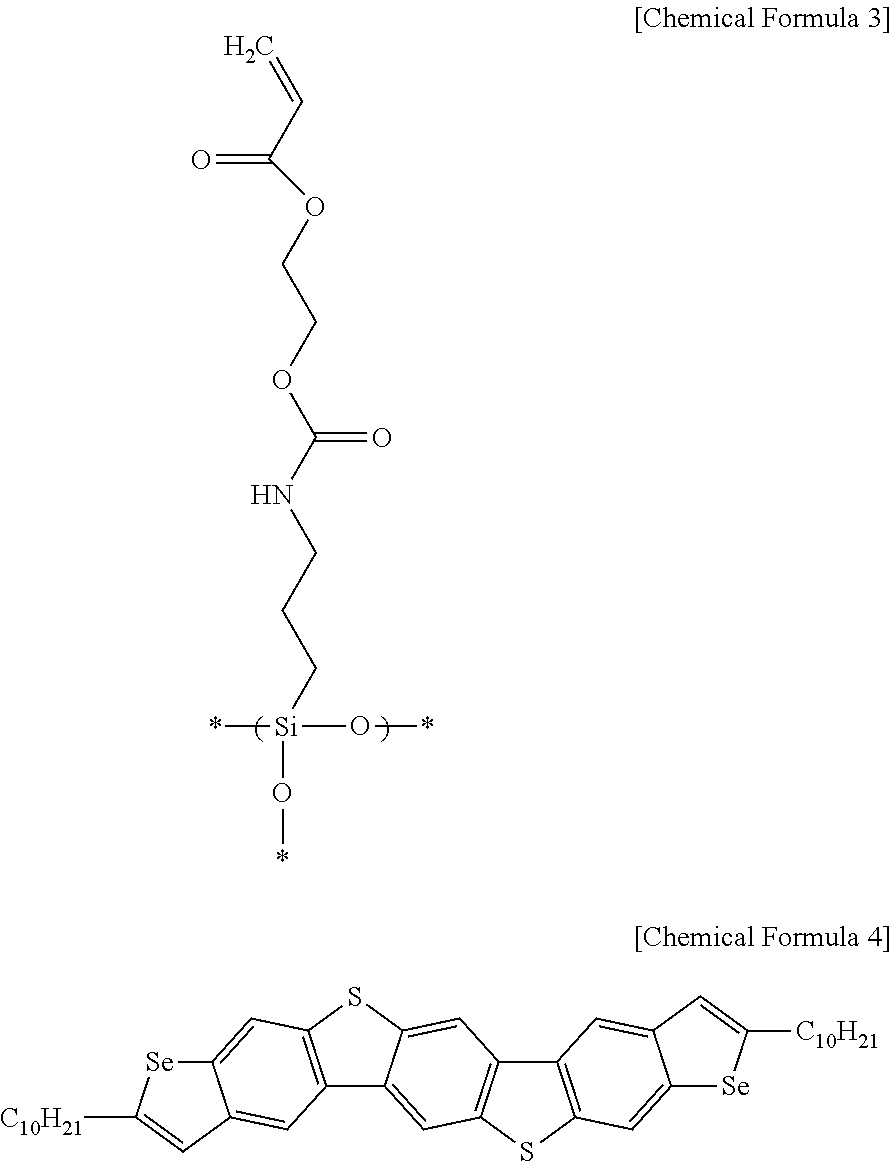
| TABLE 1 | |||
| Example 1 | Comparative Example 2 | ||
| Charge mobility (cm2/Vs) | 5.6 | 2.5 |
| on-current (A) | 4.39E−04 | 2.85E−04 |
Claims (15)


Applications Claiming Priority (2)
| Application Number | Priority Date | Filing Date | Title |
|---|---|---|---|
| KR10-2015-0182702 | 2015-12-21 | ||
| KR20150182702 | 2015-12-21 |
Publications (2)
| Publication Number | Publication Date |
|---|---|
| US20170179414A1 US20170179414A1 (en) | 2017-06-22 |
| US10727426B2 true US10727426B2 (en) | 2020-07-28 |
Family
ID=57737582
Family Applications (1)
| Application Number | Title | Priority Date | Filing Date |
|---|---|---|---|
| US15/384,968 Active US10727426B2 (en) | 2015-12-21 | 2016-12-20 | Thin film transistor, method of manufacturing the same, and electronic device including the same |
Country Status (3)
| Country | Link |
|---|---|
| US (1) | US10727426B2 (en) |
| EP (1) | EP3185322B1 (en) |
| KR (1) | KR102644976B1 (en) |
Families Citing this family (2)
| Publication number | Priority date | Publication date | Assignee | Title |
|---|---|---|---|---|
| KR102372207B1 (en) * | 2017-07-27 | 2022-03-07 | 삼성전자주식회사 | Thin film transistor and method of manufacturing the same |
| GB201810710D0 (en) * | 2018-06-29 | 2018-08-15 | Smartkem Ltd | Sputter Protective Layer For Organic Electronic Devices |
Citations (10)
| Publication number | Priority date | Publication date | Assignee | Title |
|---|---|---|---|---|
| US4861908A (en) | 1987-07-08 | 1989-08-29 | Shin-Etsu Chemical Co., Ltd. | Organosilicon compound |
| WO2003041186A2 (en) | 2001-11-05 | 2003-05-15 | 3M Innovative Properties Company | Organic thin film transistor with siloxane polymer interface |
| US20070012914A1 (en) * | 2004-03-10 | 2007-01-18 | Canon Kabushiki Kaisha | Field effect transistor, method of producing the same, and method of producing laminated member |
| JP2008298862A (en) | 2007-05-29 | 2008-12-11 | Jsr Corp | Pattern forming method and resin composition used therefor |
| US7573063B1 (en) * | 2008-05-15 | 2009-08-11 | Xerox Corporation | Organic thin film transistors |
| JP2013035274A (en) | 2011-07-13 | 2013-02-21 | Kansai Paint Co Ltd | Laminate and method of manufacturing the same |
| US20130320316A1 (en) * | 2012-06-05 | 2013-12-05 | Samsung Electronics Co., Ltd. | Fused polycyclic heteroaromatic compound, organic thin film including compound and electronic device including organic thin film |
| WO2013182328A1 (en) | 2012-06-05 | 2013-12-12 | Agfa Graphics Nv | A lithographic printing plate precursor |
| US20130337259A1 (en) * | 2012-06-14 | 2013-12-19 | E I Du Pont De Nemours And Company | Gas permeation barrier material |
| US20150243915A1 (en) * | 2014-02-25 | 2015-08-27 | Xerox Corporation | Electronic device |
-
2016
- 2016-12-20 US US15/384,968 patent/US10727426B2/en active Active
- 2016-12-21 KR KR1020160175842A patent/KR102644976B1/en active IP Right Grant
- 2016-12-21 EP EP16205716.0A patent/EP3185322B1/en active Active
Patent Citations (13)
| Publication number | Priority date | Publication date | Assignee | Title |
|---|---|---|---|---|
| US4861908A (en) | 1987-07-08 | 1989-08-29 | Shin-Etsu Chemical Co., Ltd. | Organosilicon compound |
| WO2003041186A2 (en) | 2001-11-05 | 2003-05-15 | 3M Innovative Properties Company | Organic thin film transistor with siloxane polymer interface |
| US20030102472A1 (en) * | 2001-11-05 | 2003-06-05 | 3M Innovative Properties Company | Organic thin film transistor with siloxane polymer interface |
| US20070012914A1 (en) * | 2004-03-10 | 2007-01-18 | Canon Kabushiki Kaisha | Field effect transistor, method of producing the same, and method of producing laminated member |
| JP2008298862A (en) | 2007-05-29 | 2008-12-11 | Jsr Corp | Pattern forming method and resin composition used therefor |
| US7573063B1 (en) * | 2008-05-15 | 2009-08-11 | Xerox Corporation | Organic thin film transistors |
| JP2013035274A (en) | 2011-07-13 | 2013-02-21 | Kansai Paint Co Ltd | Laminate and method of manufacturing the same |
| US20130320316A1 (en) * | 2012-06-05 | 2013-12-05 | Samsung Electronics Co., Ltd. | Fused polycyclic heteroaromatic compound, organic thin film including compound and electronic device including organic thin film |
| EP2671880A1 (en) | 2012-06-05 | 2013-12-11 | Samsung Electronics Co., Ltd | Fused polycyclic heteroaromatic compound, organic thin film including compound and electronic device including organic thin film |
| WO2013182328A1 (en) | 2012-06-05 | 2013-12-12 | Agfa Graphics Nv | A lithographic printing plate precursor |
| US20150168837A1 (en) * | 2012-06-05 | 2015-06-18 | Agfa Graphics Nv | Lithographic printing plate precusor |
| US20130337259A1 (en) * | 2012-06-14 | 2013-12-19 | E I Du Pont De Nemours And Company | Gas permeation barrier material |
| US20150243915A1 (en) * | 2014-02-25 | 2015-08-27 | Xerox Corporation | Electronic device |
Non-Patent Citations (4)
| Title |
|---|
| Chuan Liu et al., "Solution-Processable Organic Single Crystals with Bandlike Transport in Field-Effect Transistors", Advanced Materials, 2011, vol. 23 pp. 523-526. |
| European Search Report dated May 15, 2017 for corresponding European Patent Application No. 16205716.0. |
| Jihua Chen et al., "Controlled solution deposition and systematic study of charge-transport anisotropy in single crystal and single-crystal textured TIPS pentacene thin films" Organic Electronics 10, 2009, pp. 696-703. |
| W. Ou-Yang et al., "High-performance organic transistors with high-k dielectrics: A comparative study on solution-processed single crystals and vacuum-deposited polycrystalline films of 2,9-didecyl-dinaphtho[2,3-b:2′3′-f]thieno[3,2-b]thiophene", Applied Physics Letters 101, AIP Publishing, 2012. |
Also Published As
| Publication number | Publication date |
|---|---|
| US20170179414A1 (en) | 2017-06-22 |
| KR20170074212A (en) | 2017-06-29 |
| KR102644976B1 (en) | 2024-03-07 |
| EP3185322B1 (en) | 2021-04-21 |
| EP3185322A1 (en) | 2017-06-28 |
Similar Documents
| Publication | Publication Date | Title |
|---|---|---|
| US9537102B2 (en) | Fused polycyclic heteroaromatic compound, organic thin film including compound and electronic device including organic thin film | |
| US8222073B2 (en) | Fabricating TFT having fluorocarbon-containing layer | |
| US10559764B2 (en) | Fused polycyclic heteroaromatic compound, organic thin film including compound and electronic device including organic thin film | |
| US8658805B2 (en) | Fused polyheteroaromatic compound, organic thin film including the compound, and electronic device including the organic thin film | |
| US9853226B2 (en) | Fused polycyclic heteroaromatic compound, organic thin film including compound and electronic device including organic thin film | |
| US8742410B2 (en) | Fused polycyclic heteroaromatic compound, organic thin film including the compound and electronic device including the organic thin film | |
| KR101958990B1 (en) | Organic thin film transistor and method of manufacturing the same | |
| KR20110056505A (en) | Surface treated substrates for top gate organic thin film transistors | |
| Ko et al. | Electrically and thermally stable gate dielectrics from thiol–ene cross-linked systems for use in organic thin-film transistors | |
| US8994016B2 (en) | Dielectric layer for an electronic device | |
| US20120187379A1 (en) | Electronic device | |
| US8963131B2 (en) | Electronic device | |
| KR102450399B1 (en) | Thin film transistor, method of manufacturing same, and electronic device including thin same | |
| US10727426B2 (en) | Thin film transistor, method of manufacturing the same, and electronic device including the same | |
| US8134144B2 (en) | Thin-film transistor | |
| US8853347B2 (en) | Organic semiconductor compound, organic thin film including the organic semiconductor compound and electronic device including the organic thin film, and method of manufacturing the organic thin film | |
| Onojima et al. | Influence of phase-separated morphology on small molecule/polymer blend organic field-effect transistors fabricated using electrostatic spray deposition | |
| KR102259939B1 (en) | Composition for surface modification of insulator, method for surface modification of insulator, insulator, and thin film transistor | |
| US8106387B2 (en) | Organic thin film transistors | |
| KR100873997B1 (en) | The method for preparing organic thin film transistor using organic passivation layer with enhanced water-barrier property | |
| KR20090067728A (en) | Organic thin film transistor and method for preparing thereof | |
| Hamada et al. | Effective control of surface property on poly (silsesquioxane) films by chemical modification | |
| KR101386908B1 (en) | A composition for organic thin-film transistor gate insulators and a method for making the same |
Legal Events
| Date | Code | Title | Description |
|---|---|---|---|
| AS | Assignment |
Owner name: SAMSUNG ELECTRONICS CO., LTD., KOREA, REPUBLIC OF Free format text: ASSIGNMENT OF ASSIGNORS INTEREST;ASSIGNORS:CHOI, AJEONG;LEE, EUN KYUNG;KIM, JOO YOUNG;AND OTHERS;SIGNING DATES FROM 20161214 TO 20161215;REEL/FRAME:041141/0790 |
|
| STPP | Information on status: patent application and granting procedure in general |
Free format text: NON FINAL ACTION MAILED |
|
| STPP | Information on status: patent application and granting procedure in general |
Free format text: RESPONSE TO NON-FINAL OFFICE ACTION ENTERED AND FORWARDED TO EXAMINER |
|
| STPP | Information on status: patent application and granting procedure in general |
Free format text: FINAL REJECTION MAILED |
|
| STPP | Information on status: patent application and granting procedure in general |
Free format text: DOCKETED NEW CASE - READY FOR EXAMINATION |
|
| STPP | Information on status: patent application and granting procedure in general |
Free format text: PUBLICATIONS -- ISSUE FEE PAYMENT RECEIVED |
|
| STPP | Information on status: patent application and granting procedure in general |
Free format text: PUBLICATIONS -- ISSUE FEE PAYMENT VERIFIED |
|
| STCF | Information on status: patent grant |
Free format text: PATENTED CASE |
|
| MAFP | Maintenance fee payment |
Free format text: PAYMENT OF MAINTENANCE FEE, 4TH YEAR, LARGE ENTITY (ORIGINAL EVENT CODE: M1551); ENTITY STATUS OF PATENT OWNER: LARGE ENTITY Year of fee payment: 4 |