US10725703B2 - Method for writing data, memory device and data writing system - Google Patents
Method for writing data, memory device and data writing system Download PDFInfo
- Publication number
- US10725703B2 US10725703B2 US16/202,279 US201816202279A US10725703B2 US 10725703 B2 US10725703 B2 US 10725703B2 US 201816202279 A US201816202279 A US 201816202279A US 10725703 B2 US10725703 B2 US 10725703B2
- Authority
- US
- United States
- Prior art keywords
- data
- writing
- memory devices
- identification information
- memory
- Prior art date
- Legal status (The legal status is an assumption and is not a legal conclusion. Google has not performed a legal analysis and makes no representation as to the accuracy of the status listed.)
- Active, expires
Links
Images


Classifications
-
- G—PHYSICS
- G06—COMPUTING OR CALCULATING; COUNTING
- G06F—ELECTRIC DIGITAL DATA PROCESSING
- G06F3/00—Input arrangements for transferring data to be processed into a form capable of being handled by the computer; Output arrangements for transferring data from processing unit to output unit, e.g. interface arrangements
- G06F3/06—Digital input from, or digital output to, record carriers, e.g. RAID, emulated record carriers or networked record carriers
- G06F3/0601—Interfaces specially adapted for storage systems
- G06F3/0602—Interfaces specially adapted for storage systems specifically adapted to achieve a particular effect
- G06F3/061—Improving I/O performance
-
- G—PHYSICS
- G06—COMPUTING OR CALCULATING; COUNTING
- G06F—ELECTRIC DIGITAL DATA PROCESSING
- G06F3/00—Input arrangements for transferring data to be processed into a form capable of being handled by the computer; Output arrangements for transferring data from processing unit to output unit, e.g. interface arrangements
- G06F3/06—Digital input from, or digital output to, record carriers, e.g. RAID, emulated record carriers or networked record carriers
- G06F3/0601—Interfaces specially adapted for storage systems
- G06F3/0602—Interfaces specially adapted for storage systems specifically adapted to achieve a particular effect
- G06F3/0604—Improving or facilitating administration, e.g. storage management
-
- G—PHYSICS
- G06—COMPUTING OR CALCULATING; COUNTING
- G06F—ELECTRIC DIGITAL DATA PROCESSING
- G06F3/00—Input arrangements for transferring data to be processed into a form capable of being handled by the computer; Output arrangements for transferring data from processing unit to output unit, e.g. interface arrangements
- G06F3/06—Digital input from, or digital output to, record carriers, e.g. RAID, emulated record carriers or networked record carriers
- G06F3/0601—Interfaces specially adapted for storage systems
- G06F3/0602—Interfaces specially adapted for storage systems specifically adapted to achieve a particular effect
- G06F3/0608—Saving storage space on storage systems
-
- G—PHYSICS
- G06—COMPUTING OR CALCULATING; COUNTING
- G06F—ELECTRIC DIGITAL DATA PROCESSING
- G06F3/00—Input arrangements for transferring data to be processed into a form capable of being handled by the computer; Output arrangements for transferring data from processing unit to output unit, e.g. interface arrangements
- G06F3/06—Digital input from, or digital output to, record carriers, e.g. RAID, emulated record carriers or networked record carriers
- G06F3/0601—Interfaces specially adapted for storage systems
- G06F3/0628—Interfaces specially adapted for storage systems making use of a particular technique
- G06F3/0638—Organizing or formatting or addressing of data
- G06F3/064—Management of blocks
- G06F3/0641—De-duplication techniques
-
- G—PHYSICS
- G06—COMPUTING OR CALCULATING; COUNTING
- G06F—ELECTRIC DIGITAL DATA PROCESSING
- G06F3/00—Input arrangements for transferring data to be processed into a form capable of being handled by the computer; Output arrangements for transferring data from processing unit to output unit, e.g. interface arrangements
- G06F3/06—Digital input from, or digital output to, record carriers, e.g. RAID, emulated record carriers or networked record carriers
- G06F3/0601—Interfaces specially adapted for storage systems
- G06F3/0628—Interfaces specially adapted for storage systems making use of a particular technique
- G06F3/0655—Vertical data movement, i.e. input-output transfer; data movement between one or more hosts and one or more storage devices
- G06F3/0659—Command handling arrangements, e.g. command buffers, queues, command scheduling
-
- G—PHYSICS
- G06—COMPUTING OR CALCULATING; COUNTING
- G06F—ELECTRIC DIGITAL DATA PROCESSING
- G06F3/00—Input arrangements for transferring data to be processed into a form capable of being handled by the computer; Output arrangements for transferring data from processing unit to output unit, e.g. interface arrangements
- G06F3/06—Digital input from, or digital output to, record carriers, e.g. RAID, emulated record carriers or networked record carriers
- G06F3/0601—Interfaces specially adapted for storage systems
- G06F3/0668—Interfaces specially adapted for storage systems adopting a particular infrastructure
- G06F3/0671—In-line storage system
- G06F3/0673—Single storage device
- G06F3/0679—Non-volatile semiconductor memory device, e.g. flash memory, one time programmable memory [OTP]
-
- G—PHYSICS
- G06—COMPUTING OR CALCULATING; COUNTING
- G06F—ELECTRIC DIGITAL DATA PROCESSING
- G06F3/00—Input arrangements for transferring data to be processed into a form capable of being handled by the computer; Output arrangements for transferring data from processing unit to output unit, e.g. interface arrangements
- G06F3/06—Digital input from, or digital output to, record carriers, e.g. RAID, emulated record carriers or networked record carriers
- G06F3/0601—Interfaces specially adapted for storage systems
- G06F3/0668—Interfaces specially adapted for storage systems adopting a particular infrastructure
- G06F3/0671—In-line storage system
- G06F3/0683—Plurality of storage devices
- G06F3/0688—Non-volatile semiconductor memory arrays
Definitions
- the present invention relates to a method for writing data to a memory device.
- a writing process is performed with respect to a semiconductor memory device after assembly of the device and before shipment.
- data which is specific to the device (hereinafter referred to as “unique data”) is written.
- unique data data which is specific to the device.
- a process for writing trimming data is performed in order to adjust dispersion in manufacturing.
- each of the devices is written with unique data different per device.
- a semiconductor memory device providing means for calculating trimming value internally in each semiconductor device is suggested so as to avoid complicated process flows and errors raised in the writing of the trimming data to the plurality of semiconductor memory devices. (for example, Japanese Patent Application Laid-Open No. 2007-164865).
- the writing device When the unique data which is target of writing cannot be generated internally in each semiconductor memory device, data have to be written in each semiconductor memory device in serial by a writing device such as writer.
- the writing device performs writing the unique data into a plurality of semiconductor devices by repeating a set of operation times as much as a number of the semiconductor memory devices.
- the set of operation includes reading-out the unique data from its database and writing the unique data into corresponding semiconductor memory device.
- serial writing of the unique data writing operation is performed to each of the semiconductor memory devices one by one in sequence so that process time is required. Length of the process time is proportional to the number of the semiconductor memory devices.
- each semiconductor memory device which is target of the writing is required to be powered on, thereby length of time required to activate the semiconductor memory device increases in proportion to the number of the semiconductor memory devices.
- It is therefore an object of the present invention is to provide a method for writing data which is capable of writing unique data into a plurality of memory devices within a short process time.
- a method for writing data according to the present invention is performed by a data writing system constituted by a plurality of memory devices and a writing device which writes data into the plurality of memory devices.
- the method includes: data maintaining step at the writing device, for maintaining writing object data to each of the plurality of memory devices; obtaining step at the writing device, for obtaining identification information assigned to each of the plurality of memory devices from the plurality of memory devices; generating step at the writing device, for generating combination data by associating and combining the identification information and the writing object data with respect to the plurality of memory devices; sending step at the writing device, for sending the combination data to the plurality of memory devices; receiving step at each of the plurality of memory devices, for receiving the combination data; extracting step at each of the plurality of memory devices, for extracting the writing object data corresponding to the memory device on the basis of the identification information from the combination data; and memorizing step at each of the plurality of memory devices, for memorizing the target data for writing extracted from the combination data.
- a memory device is a memory device which memorizes data comprising: a nonvolatile memory; a writing circuit configured to write data in the nonvolatile memory; a buffer configured to store the writing object data temporarily; a receiving part configured to receive a combination data which is obtained by associating and combining identification information with respect to a plurality of memory devices and writing object data, and a writing signal which indicates writing of data into the nonvolatile memory; and a comparing part configured to compare the identification information memorized in an identification information memorizing part and identification information with respect to the plurality of memory devices included in the combination data; wherein the comparing part extracts writing object data corresponding to the memory device from the combination data on the basis of a result of the comparison, the buffer stores temporarily the writing object data extracted by the comparing part, the writing circuit writes the writing object data which is read out from the buffer into the nonvolatile memory in response to the writing signal.
- FIG. 1 is a block diagram showing a configuration of a data writing system of a first embodiment
- FIG. 2 is a block diagram showing a configuration of a writing device and a memory device of the first embodiment
- FIG. 3A is a schematic diagram showing an example of data stored in a unique data DB
- FIG. 3B is a schematic diagram showing contents of a combination data
- FIG. 4 is a schematic diagram showing transmission of the combination data in the first embodiment
- FIG. 5 is a flow chart showing a process of a data writing process in the first embodiment
- FIG. 6 is a flow chart showing a data storage process in the memory device of the first embodiment.
- FIG. 7 is a schematic diagram showing transmission of the unique data in a comparative example.
- FIG. 8 is a flow chart showing a process of a data writing process in the comparative example
- FIG. 9 is a block diagram showing a configuration of a writing device and a memory device of a second embodiment
- FIG. 10 is a flow chart showing a data storage process in the memory device of the second embodiment.
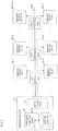
- FIG. 1 is a block diagram showing a configuration of a data writing system of the present embodiment.
- a data writing system 100 in the present embodiment is constituted by a writing device 10 and a plurality of memory devices 20 - 1 to 20 - n (n: integer number greater than or equal to 2).
- the writing device 10 and the memory devices 20 - 1 to 20 - n are connected to each other through data bus line DBL.
- a unique ID is assigned to each of the memory devices 20 - 1 to 20 - n as an identification information for identifying each devices.
- ID- 1 is assigned to the memory device 20 - 1
- ID- 2 is assigned to the memory device 20 - 2
- ID- 3 is assigned to the memory device 20 - 3
- ID- 4 is assigned to the memory device 20 - 4
- ID- 5 is assigned to the memory device 20 - 5
- ID- 6 is assigned to the memory device 20 - 6
- ID-(n ⁇ 1) is assigned to the memory device 20 -( n ⁇ 1)
- ID-n is assigned to the memory device 20 - n.
- FIG. 2 is a block diagram showing a configuration of the writing device 10 and one of the memory devices 20 - 1 to 20 - n (hereinafter referred to as memory device 20 ).
- the writing device 10 is a writer which writes data into a semiconductor memory device.
- the writing device 10 comprises a unique data DB (database) 11 , a process control part 12 and an interface part 13 .
- FIG. 3A is a schematic diagram showing an example of data stored in the unique data DB 11 .
- Unique data UD 1 to UDn corresponding to the respective memory devices 20 - 1 to 20 - n are stored in the unique data DB 11 in association with ID- 1 to ID-n which are unique IDs of respective memory devices.
- the unique data UD 1 to UDn become target of writing into the memory devices 20 - 1 to 20 - n in a data writing process performed by the data writing system 100 of the present embodiment.
- Unique data (e.g. UDX) of a memory device other than the memory devices 20 - 1 to 20 - n is stored in the unique data DB 11 in associated with unique ID (e.g. ID-X) of the other memory device.
- the process control part 12 performs various data processing and controls each block of the writing device 10 in the data writing process of the present embodiment. Specifically, the process control part 12 reads out unique data from the unique data DB 11 based on unique ID which is received by the interface part 13 from the memory devices 20 - 1 to 20 - n . The process control part 12 reads out unique data corresponding to that unique ID.
- the process control part 12 generates combination data CD based on the unique data which is read out by the process control part 12 .
- the process control part 12 obtains unique ID of the memory devices 20 - 1 to 20 - n which are target of writing with unique data in the present embodiment.
- the process control part 12 searches and extracts unique data UD 1 to UDn corresponding to the unique ID that the process control part 12 obtains from the unique data DB 11 . Then, the process control part 12 generates the combination data CD by combining the unique ID and the unique data.
- FIG. 3B is a schematic diagram showing contents included in the combination data CD.
- the combination data CD is constituted as one data combining a plurality of unique ID, ID- 1 to ID-n, and corresponding unique data UD 1 to UDn.
- the process control part 12 generates a parallel writing signal PWS which indicates to write unique data into the memory devices 20 - 1 to 20 - n in parallel.
- the interface part 13 receives unique ID from the memory devices 20 - 1 to 20 - n through data bus line DBL.
- the interface part 13 sends combination data CD and the parallel writing signal PWS to the memory devices 20 - 1 to 20 - n through data bus line DBL.
- the same combination data CD and the parallel writing signal PWS are supplied to the memory devices 20 - 1 to 20 - n from the writing device 10 through data bus line DBL.
- the memory device 20 comprises a flash controller 21 and a flash memory 22 .
- the flash controller 21 is a control part which controls the flash memory 22 which is a nonvolatile memory device.
- the flash controller 21 includes an interface part 23 , a buffer 24 , a unique ID memory part 25 , a CPU 26 , a writing circuit 27 and a read out circuit 28 .
- the interface part 23 receives the combination data CD and the parallel writing signal PWS which are sent from the writing device 10 through data bus line DBL.
- the interface part 23 sends the unique ID memorized in the unique ID memory part 25 to the writing device 10 .
- the buffer 24 temporarily stores the combination data CD which is received by the interface part 23 .
- the unique ID memory part 25 memorizes the unique ID which is a specific identification information assigned to the memory device 20 .
- the CPU (Central Processing Unit) 26 controls each block in the flash controller 21 .
- the CPU 26 reads out the unique ID from the unique ID memory part 25 and extracts the unique data corresponding to that unique ID from the combination data CD stored in the buffer 24 .
- the CPU 26 supplies the extracted unique data to the writing circuit 27 .
- the writing circuit 27 writes data in the flash memory 22 in response to the parallel writing signal PWS which is received by the interface part 23 .
- the read out circuit 28 reads out data from the flash memory 22 .
- the flash memory 22 includes a unique data storage part 29 which becomes writing destination of writing the unique data by the writing circuit 27 .
- a process operation of data writing process in the data writing system in the present embodiment is described below referring to a flow chart illustrated in FIG. 5 .
- the interface part 13 in the writing device 10 receives the unique IDs from the memory devices 20 - 1 to 20 - n through the data bus line DBL.
- the process control part 12 obtains the unique IDs of the memory devices 20 - 1 to 20 - n which is received by the interface part 13 (step S 101 ).
- the process control part 12 accesses the unique data DB 11 and searches the unique data corresponding to the unique IDs (i.e. ID- 1 to ID-n) which have been obtained in the step S 101 (step S 102 ).
- the process control part 12 extracts the unique data which has been searched (i.e. UD 1 to UDn) from the unique data DB 11 (step S 103 ).
- the process control part 12 generates the combination data CD by combining the extracted unique data UD 1 -UDn and unique IDs, ID- 1 to ID-n, corresponding to the unique data (step S 104 ).
- the interface part 13 sends the combination data CD in parallel to the memory devices 20 - 1 to 20 - n in response to the control by the process control part 12 (step S 105 ).
- the process control part 12 sends the parallel writing signal PWS to the memory devices 20 - 1 to 20 - n through the interface part 13 after completion of sending the combination data CD to all of the memory devices (step S 106 ).
- the parallel writing signal PWS is indicative of writing the unique data in parallel to the memory devices 20 - 1 to 20 - n.
- the memory devices 20 - 1 to 20 - n performs a data storage process (step S 107 ).
- the interface part 23 of the memory devices 20 - 1 to 20 - n receives the combination data CD (step S 201 ).
- the buffer 24 stores the received combination data CD temporarily (step S 202 ).
- the CPU 26 of the memory devices 20 - 1 to 20 - n detects the unique data corresponding to the unique ID of the memory devices (i.e. the unique ID memorized in the unique ID memory part 25 ) from the combination data CD stored in the buffer 24 (step S 203 ).
- the interface part 23 receives the parallel writing signal PWS (step S 204 ).
- the writing circuit 27 stores the unique data detected in the step S 203 in the unique data storage part 29 of the flash memory 22 in response to the parallel writing signal PWS (step S 205 ).
- the writing unique data in the memory devices 20 - 1 to 20 - n is completed by the above-mentioned steps.
- the combination data CD is sent to the memory devices 20 - 1 to 20 - n in parallel.
- Each of the memory devices performs detection and storage of the unique data corresponding to that each memory device.
- a comparative example which is different from the data writing system 100 in the present embodiment is described below referring to FIG. 7 and FIG. 8 .
- the writing device 10 does not send the combination data CD and performs writing by sending merely the unique data corresponding to each memory device.
- the writing device 10 sends only the unique data (UD- 1 to UD-n) specific to each memory device to the memory devices 20 - 1 to 20 - n .
- the writing device 10 sends the unique data UD 1 to the memory device 20 - 1 , the unique data UD 2 to the memory device 20 - 2 , the unique data UD 3 to the memory device 20 - 3 , the unique data UD 4 to the memory device 20 - 4 , the unique data UD(n ⁇ 1) to the memory device 20 -( n ⁇ 1), and the unique data UDn to the memory device 20 - n respectively.
- FIG. 8 is a flow chart showing a process operation of a data writing process in the data writing system of the comparative example.
- the interface part 13 in the writing device 10 receives the unique ID from memory devices 20 - 1 to 20 - n through the data bus line DBL.
- the process control part 12 obtains the unique data UD 1 to UDn of the memory devices (step S 301 ).
- step S 302 all of the memory devices 20 - 1 to 20 - n are turned off temporarily by stopping power supply to the memory devices 20 - 1 to 20 - n from external power source (not shown) provided out of the data writing system.
- the process control part 12 searches and extracts the unique data UDm corresponding to ID-m which is the unique ID of the memory device 20 - m from the unique data DB 11 (step S 304 ).
- the memory device 20 - m is turned on by restarting the power supply from the external power source to the memory device 20 - m (step S 305 ).
- the interface part 13 sends the unique data UDm to the memory device 20 - m in response to the control by the process control part 12 (step S 306 ).
- the memory device 20 - m stores the unique data UDm in its memory (step S 307 ).
- step S 308 When the process control part 12 determines that the storing of the unique data is not completed (step S 308 : No), the process control part 12 increments the value m by one and returns to the step S 304 (step S 309 ).
- the writing of the unique data to the memory devices 20 - 1 to 20 - n is completed through above-mentioned steps.
- the combination data CD is sent to each memory device in parallel in the data writing process of the present embodiment as described referring to FIG. 5 . It is not necessary to send data in a serial manner repeatedly in contrast to the comparative embodiment. Accordingly, length of time to send data is not increased in total although size of the combination data CD is larger than that of the individual unique data.
- a set of process is performed in a state that all of the memory devices 20 - 1 to 20 - n are turned on. It is not necessary to turn on each of the memory devices in each process.
- storing the unique data to each of the memory devices is performed in parallel in response to the parallel writing signal PWS. It is not necessary to perform storing the unique data to each of the memory devices in a serial manner repeatedly as the comparative example.
- required time to turn on the memory device and to store the unique data in the memory device is reduced so that writing unique data into the plurality of the memory devices in short process time becomes possible.
- FIG. 9 is a block diagram showing a configuration of a writing device 10 and one of the memory devices 20 - 1 to 20 - n (hereinafter referred to as memory device 20 ) included in a data writing system which is an embodiment of the present invention.
- the writing device 10 comprises a unique data DB 11 , a process control part 12 and an interface part 13 . Configuration and operation of these elements of the writing devices 10 are equivalent to the corresponding elements appearing in the first embodiment.
- the memory device 20 comprises a flash controller 21 and a flash memory 22 .
- the flash controller 21 includes an interface part 23 , a buffer 24 , a unique ID memory part 25 , a writing circuit 27 and a read out circuit 28 .
- the memory device 20 has a comparator 30 .
- the comparator 30 compares the unique ID memorized in the unique ID memory part 25 and the unique ID included in the combination data CD (i.e. combination ID received by the interface part 23 ) which is sent from the writing device 10 . When the unique IDs coincide with each other, the comparator 30 extracts unique data corresponding to that unique ID from the combination data CD and stores the unique data in the buffer 24 .
- Data storage process performed by the memory device 20 in the data writing process of the present embodiment is described referring to FIG. 5
- the steps before the data storage process are in the same manner as the process in the first embodiment as shown in FIG. 5 .
- the interface part 23 of the memory device 20 receives the combination data CD (step S 401 ).
- the comparator 30 reads out the unique ID from the unique ID memory part 25 and compares that unique ID with the unique ID included in the combination data CD (step S 402 ).
- the comparator 30 extracts the unique data corresponding to that unique ID from the combination data CD and stores the unique data in the buffer 24 (step S 403 ).
- the interface part 23 receives the parallel writing signal PWS (step S 404 ).
- the writing circuit 27 reads out the unique data stored in the buffer 24 and stores the unique data in the unique data storage part 29 of the flash memory 22 in response to the parallel writing signal PWS (step S 405 ).
- the memory device 20 performs the process in a state that all of the memory devices 20 - 1 to 20 - n are turned on. Storing of the unique data into each memory device is performed in parallel. It is therefore the required time to turn on the memory devices and to store the unique data into the memory device is reduced. It becomes possible to perform writing of the unique data into a plurality of memory devices in shorter process time.
- the memory device 20 stores only the unique data corresponding to the unique ID which coincides with its own unique ID (i.e. the unique ID memorized in the unique ID memory part 25 ) into the buffer 24 .
- Data amount of the data stored in the buffer 24 can be reduced in comparison to a case that the combination data CD is stored in the buffer 24 . Therefore, the buffer size can be reduced.
- the memory device includes the flash memory as a memory which memorizes data.
- type of the memory is not limited to the flash memory. It is merely required that the memory device includes a nonvolatile memory.
- the unique data is searched from the combination data CD under the condition of coincidence of the unique ID as an example.
- Error detecting code such as CRC (Cyclic Redundancy Check), or error correction code such as ECC may be added to the unique ID.
- the unique data may be identified under the condition of coincidence of the unique ID and the code. According to such configuration, for example, it is possible to identify the unique data with a high degree of accuracy although in case error can be arisen in selected data (e.g. duplicated data between semiconductor memory devices) searched by only unique ID when the inputted unique ID is changed into garbled bits by noise.
Landscapes
- Engineering & Computer Science (AREA)
- Theoretical Computer Science (AREA)
- Human Computer Interaction (AREA)
- Physics & Mathematics (AREA)
- General Engineering & Computer Science (AREA)
- General Physics & Mathematics (AREA)
- Read Only Memory (AREA)
- Memory System (AREA)
- Techniques For Improving Reliability Of Storages (AREA)
- Information Retrieval, Db Structures And Fs Structures Therefor (AREA)
Abstract
Description
Claims (6)
Applications Claiming Priority (2)
| Application Number | Priority Date | Filing Date | Title |
|---|---|---|---|
| JP2017-229044 | 2017-11-29 | ||
| JP2017229044A JP7012520B2 (en) | 2017-11-29 | 2017-11-29 | Data writing method and storage device |
Publications (2)
| Publication Number | Publication Date |
|---|---|
| US20190163402A1 US20190163402A1 (en) | 2019-05-30 |
| US10725703B2 true US10725703B2 (en) | 2020-07-28 |
Family
ID=66633140
Family Applications (1)
| Application Number | Title | Priority Date | Filing Date |
|---|---|---|---|
| US16/202,279 Active 2039-01-24 US10725703B2 (en) | 2017-11-29 | 2018-11-28 | Method for writing data, memory device and data writing system |
Country Status (3)
| Country | Link |
|---|---|
| US (1) | US10725703B2 (en) |
| JP (1) | JP7012520B2 (en) |
| CN (1) | CN109841249B (en) |
Citations (2)
| Publication number | Priority date | Publication date | Assignee | Title |
|---|---|---|---|---|
| JP2007164865A (en) | 2005-12-12 | 2007-06-28 | Matsushita Electric Ind Co Ltd | Semiconductor memory device |
| US20120221767A1 (en) * | 2011-02-28 | 2012-08-30 | Apple Inc. | Efficient buffering for a system having non-volatile memory |
Family Cites Families (4)
| Publication number | Priority date | Publication date | Assignee | Title |
|---|---|---|---|---|
| JP4453314B2 (en) * | 2003-09-19 | 2010-04-21 | セイコーエプソン株式会社 | Storage device that can read and write in multiple modes |
| CN100472496C (en) * | 2005-03-17 | 2009-03-25 | 富士通株式会社 | data transmission device |
| JP2012053579A (en) * | 2010-08-31 | 2012-03-15 | Iix Inc | Production management system and production management method |
| JP5672927B2 (en) * | 2010-10-08 | 2015-02-18 | セイコーエプソン株式会社 | Storage device, host device, circuit board, liquid container and system |
-
2017
- 2017-11-29 JP JP2017229044A patent/JP7012520B2/en not_active Expired - Fee Related
-
2018
- 2018-11-28 US US16/202,279 patent/US10725703B2/en active Active
- 2018-11-29 CN CN201811443373.0A patent/CN109841249B/en active Active
Patent Citations (2)
| Publication number | Priority date | Publication date | Assignee | Title |
|---|---|---|---|---|
| JP2007164865A (en) | 2005-12-12 | 2007-06-28 | Matsushita Electric Ind Co Ltd | Semiconductor memory device |
| US20120221767A1 (en) * | 2011-02-28 | 2012-08-30 | Apple Inc. | Efficient buffering for a system having non-volatile memory |
Also Published As
| Publication number | Publication date |
|---|---|
| JP7012520B2 (en) | 2022-01-28 |
| US20190163402A1 (en) | 2019-05-30 |
| CN109841249B (en) | 2024-03-08 |
| CN109841249A (en) | 2019-06-04 |
| JP2019101547A (en) | 2019-06-24 |
Similar Documents
| Publication | Publication Date | Title |
|---|---|---|
| US7412575B2 (en) | Data management technique for improving data reliability | |
| US9202591B2 (en) | On-line memory testing systems and methods | |
| US10795763B2 (en) | Memory system and error correcting method thereof | |
| KR20000052798A (en) | Method and apparatus for correcting a multilevel cell memory by using error locating codes | |
| CN103077095B (en) | Error correction method and device for stored data and computer system | |
| CN111078459A (en) | Method, device and system for testing semiconductor chip | |
| CN111124742B (en) | Flash data verification method, Flash controller, storage medium, and device | |
| CN105045721A (en) | Method and device for checking data consistency | |
| US10613918B2 (en) | Data register monitoring | |
| US6957377B2 (en) | Marking of and searching for initial defective blocks in semiconductor memory | |
| US20170123905A1 (en) | Non-volatile memory device and read method thereof | |
| CN111176884A (en) | SEC (Security and Security) verification method and device for FPGA (field programmable Gate array) configuration memory | |
| KR101205628B1 (en) | Semiconductor memory device and read method thereof | |
| US10725703B2 (en) | Method for writing data, memory device and data writing system | |
| US11231990B2 (en) | Device and method for generating error correction information | |
| US20040230879A1 (en) | Apparatus and method for responding to data retention loss in a non-volatile memory unit using error checking and correction techniques | |
| US11249839B1 (en) | Method and apparatus for memory error detection | |
| US10176043B2 (en) | Memory controller | |
| US10379926B2 (en) | Method and device for monitoring data error status in a memory | |
| US20190163380A1 (en) | Rewriting checking device, rewriting checking method, and non-transitory computer readable medium for rewriting checking | |
| US10720222B2 (en) | Solid state storage device using state prediction method | |
| US20220365843A1 (en) | Method for detecting flash memory module and associated system on chip | |
| US20090327562A1 (en) | Implementing Bus Interface Calibration for Enhanced Bus Interface Initialization Time | |
| US20190324852A1 (en) | Semiconductor integrated circuit, storage device, and error correction method | |
| US20250103240A1 (en) | Control device, detection method, and non-transitory computer-readable medium storing detection program |
Legal Events
| Date | Code | Title | Description |
|---|---|---|---|
| AS | Assignment |
Owner name: LAPIS SEMICONDUCTOR CO., LTD., JAPAN Free format text: ASSIGNMENT OF ASSIGNORS INTEREST;ASSIGNOR:YAMAUCHI, SAKU;REEL/FRAME:048156/0512 Effective date: 20181127 |
|
| FEPP | Fee payment procedure |
Free format text: ENTITY STATUS SET TO UNDISCOUNTED (ORIGINAL EVENT CODE: BIG.); ENTITY STATUS OF PATENT OWNER: LARGE ENTITY |
|
| STPP | Information on status: patent application and granting procedure in general |
Free format text: DOCKETED NEW CASE - READY FOR EXAMINATION |
|
| STPP | Information on status: patent application and granting procedure in general |
Free format text: NOTICE OF ALLOWANCE MAILED -- APPLICATION RECEIVED IN OFFICE OF PUBLICATIONS |
|
| STPP | Information on status: patent application and granting procedure in general |
Free format text: PUBLICATIONS -- ISSUE FEE PAYMENT VERIFIED |
|
| STCF | Information on status: patent grant |
Free format text: PATENTED CASE |
|
| MAFP | Maintenance fee payment |
Free format text: PAYMENT OF MAINTENANCE FEE, 4TH YEAR, LARGE ENTITY (ORIGINAL EVENT CODE: M1551); ENTITY STATUS OF PATENT OWNER: LARGE ENTITY Year of fee payment: 4 |