US10721441B2 - Structured plane illumination microscopy - Google Patents
Structured plane illumination microscopy Download PDFInfo
- Publication number
- US10721441B2 US10721441B2 US16/044,449 US201816044449A US10721441B2 US 10721441 B2 US10721441 B2 US 10721441B2 US 201816044449 A US201816044449 A US 201816044449A US 10721441 B2 US10721441 B2 US 10721441B2
- Authority
- US
- United States
- Prior art keywords
- bessel
- beams
- sample
- plane
- light
- Prior art date
- Legal status (The legal status is an assumption and is not a legal conclusion. Google has not performed a legal analysis and makes no representation as to the accuracy of the status listed.)
- Active
Links
- 238000005286 illumination Methods 0.000 title description 97
- 238000000386 microscopy Methods 0.000 title description 27
- 238000001514 detection method Methods 0.000 claims abstract description 87
- 238000003384 imaging method Methods 0.000 claims abstract description 66
- 230000001427 coherent effect Effects 0.000 claims abstract description 40
- 230000005284 excitation Effects 0.000 claims description 235
- 230000005855 radiation Effects 0.000 claims description 189
- 230000003287 optical effect Effects 0.000 claims description 113
- 238000000034 method Methods 0.000 claims description 102
- 230000004913 activation Effects 0.000 claims description 89
- 230000008569 process Effects 0.000 claims description 45
- 238000010408 sweeping Methods 0.000 claims description 16
- 230000003213 activating effect Effects 0.000 claims description 8
- 230000001066 destructive effect Effects 0.000 claims description 8
- 238000010521 absorption reaction Methods 0.000 claims description 3
- 230000007274 generation of a signal involved in cell-cell signaling Effects 0.000 claims description 3
- 230000006870 function Effects 0.000 description 87
- 238000010586 diagram Methods 0.000 description 57
- 230000005684 electric field Effects 0.000 description 31
- 230000010363 phase shift Effects 0.000 description 22
- 210000004027 cell Anatomy 0.000 description 21
- 235000021251 pulses Nutrition 0.000 description 20
- 108091006047 fluorescent proteins Proteins 0.000 description 14
- 102000034287 fluorescent proteins Human genes 0.000 description 14
- 238000012546 transfer Methods 0.000 description 12
- 230000004807 localization Effects 0.000 description 11
- 230000001902 propagating effect Effects 0.000 description 11
- 230000000694 effects Effects 0.000 description 10
- 230000005281 excited state Effects 0.000 description 10
- 230000002829 reductive effect Effects 0.000 description 10
- 241000894007 species Species 0.000 description 9
- 238000004590 computer program Methods 0.000 description 8
- 238000004624 confocal microscopy Methods 0.000 description 8
- 239000002609 medium Substances 0.000 description 8
- 102000004169 proteins and genes Human genes 0.000 description 8
- 108090000623 proteins and genes Proteins 0.000 description 8
- 230000008901 benefit Effects 0.000 description 7
- 230000000737 periodic effect Effects 0.000 description 7
- 210000001747 pupil Anatomy 0.000 description 7
- 230000003595 spectral effect Effects 0.000 description 7
- 230000005540 biological transmission Effects 0.000 description 5
- 230000003993 interaction Effects 0.000 description 5
- 230000015654 memory Effects 0.000 description 5
- 230000008832 photodamage Effects 0.000 description 5
- 230000010287 polarization Effects 0.000 description 5
- 206010034972 Photosensitivity reaction Diseases 0.000 description 4
- 238000013459 approach Methods 0.000 description 4
- 239000002131 composite material Substances 0.000 description 4
- 230000007423 decrease Effects 0.000 description 4
- 230000006872 improvement Effects 0.000 description 4
- 208000007578 phototoxic dermatitis Diseases 0.000 description 4
- 231100000018 phototoxicity Toxicity 0.000 description 4
- 230000004075 alteration Effects 0.000 description 3
- 238000004061 bleaching Methods 0.000 description 3
- 230000002939 deleterious effect Effects 0.000 description 3
- 230000005283 ground state Effects 0.000 description 3
- 238000010859 live-cell imaging Methods 0.000 description 3
- 239000000463 material Substances 0.000 description 3
- 238000012545 processing Methods 0.000 description 3
- 230000004044 response Effects 0.000 description 3
- 239000013598 vector Substances 0.000 description 3
- KPKZJLCSROULON-QKGLWVMZSA-N Phalloidin Chemical compound N1C(=O)[C@@H]([C@@H](O)C)NC(=O)[C@H](C)NC(=O)[C@H](C[C@@](C)(O)CO)NC(=O)[C@H](C2)NC(=O)[C@H](C)NC(=O)[C@@H]3C[C@H](O)CN3C(=O)[C@@H]1CSC1=C2C2=CC=CC=C2N1 KPKZJLCSROULON-QKGLWVMZSA-N 0.000 description 2
- 230000031016 anaphase Effects 0.000 description 2
- 230000004323 axial length Effects 0.000 description 2
- 230000001413 cellular effect Effects 0.000 description 2
- 210000001520 comb Anatomy 0.000 description 2
- 230000007613 environmental effect Effects 0.000 description 2
- 238000001914 filtration Methods 0.000 description 2
- 238000000799 fluorescence microscopy Methods 0.000 description 2
- 239000005090 green fluorescent protein Substances 0.000 description 2
- 230000002427 irreversible effect Effects 0.000 description 2
- 239000004973 liquid crystal related substance Substances 0.000 description 2
- 238000012986 modification Methods 0.000 description 2
- 230000004048 modification Effects 0.000 description 2
- 210000004940 nucleus Anatomy 0.000 description 2
- 230000000135 prohibitive effect Effects 0.000 description 2
- 230000000644 propagated effect Effects 0.000 description 2
- 108010054624 red fluorescent protein Proteins 0.000 description 2
- 230000003068 static effect Effects 0.000 description 2
- 238000013519 translation Methods 0.000 description 2
- HONKEGXLWUDTCF-YFKPBYRVSA-N (2s)-2-amino-2-methyl-4-phosphonobutanoic acid Chemical compound OC(=O)[C@](N)(C)CCP(O)(O)=O HONKEGXLWUDTCF-YFKPBYRVSA-N 0.000 description 1
- 102000007469 Actins Human genes 0.000 description 1
- 108010085238 Actins Proteins 0.000 description 1
- 241000242764 Aequorea victoria Species 0.000 description 1
- 239000012109 Alexa Fluor 568 Substances 0.000 description 1
- 108010031426 Anemonia sulcata FP595 protein Proteins 0.000 description 1
- 102000014914 Carrier Proteins Human genes 0.000 description 1
- 241000282552 Chlorocebus aethiops Species 0.000 description 1
- 108091060290 Chromatid Proteins 0.000 description 1
- 108020004414 DNA Proteins 0.000 description 1
- 238000006424 Flood reaction Methods 0.000 description 1
- 108010043121 Green Fluorescent Proteins Proteins 0.000 description 1
- 102000004144 Green Fluorescent Proteins Human genes 0.000 description 1
- 102000006947 Histones Human genes 0.000 description 1
- 108010033040 Histones Proteins 0.000 description 1
- 101000616438 Homo sapiens Microtubule-associated protein 4 Proteins 0.000 description 1
- 102100026517 Lamin-B1 Human genes 0.000 description 1
- 102000003960 Ligases Human genes 0.000 description 1
- 108090000364 Ligases Proteins 0.000 description 1
- 108091022875 Microtubule Proteins 0.000 description 1
- 102000029749 Microtubule Human genes 0.000 description 1
- 102100021794 Microtubule-associated protein 4 Human genes 0.000 description 1
- 241000283283 Orcinus orca Species 0.000 description 1
- 108010009711 Phalloidine Proteins 0.000 description 1
- 235000010627 Phaseolus vulgaris Nutrition 0.000 description 1
- 244000046052 Phaseolus vulgaris Species 0.000 description 1
- 238000001069 Raman spectroscopy Methods 0.000 description 1
- 102000001332 SRC Human genes 0.000 description 1
- 108060006706 SRC Proteins 0.000 description 1
- 238000009825 accumulation Methods 0.000 description 1
- 239000012736 aqueous medium Substances 0.000 description 1
- 230000006399 behavior Effects 0.000 description 1
- 230000009286 beneficial effect Effects 0.000 description 1
- 108091008324 binding proteins Proteins 0.000 description 1
- 238000012984 biological imaging Methods 0.000 description 1
- 229960002685 biotin Drugs 0.000 description 1
- YBJHBAHKTGYVGT-ZKWXMUAHSA-N biotin Natural products N1C(=O)N[C@@H]2[C@H](CCCCC(=O)O)SC[C@@H]21 YBJHBAHKTGYVGT-ZKWXMUAHSA-N 0.000 description 1
- 235000020958 biotin Nutrition 0.000 description 1
- 239000011616 biotin Substances 0.000 description 1
- 239000007844 bleaching agent Substances 0.000 description 1
- 239000000969 carrier Substances 0.000 description 1
- 230000030833 cell death Effects 0.000 description 1
- 230000033077 cellular process Effects 0.000 description 1
- 210000003850 cellular structure Anatomy 0.000 description 1
- 230000008859 change Effects 0.000 description 1
- 210000004756 chromatid Anatomy 0.000 description 1
- 210000000349 chromosome Anatomy 0.000 description 1
- 230000008045 co-localization Effects 0.000 description 1
- 238000004891 communication Methods 0.000 description 1
- 239000000470 constituent Substances 0.000 description 1
- 238000010276 construction Methods 0.000 description 1
- 108010082025 cyan fluorescent protein Proteins 0.000 description 1
- 210000004292 cytoskeleton Anatomy 0.000 description 1
- 230000006378 damage Effects 0.000 description 1
- 230000009849 deactivation Effects 0.000 description 1
- 230000003247 decreasing effect Effects 0.000 description 1
- 239000000539 dimer Substances 0.000 description 1
- 230000008846 dynamic interplay Effects 0.000 description 1
- 210000002472 endoplasmic reticulum Anatomy 0.000 description 1
- 238000005516 engineering process Methods 0.000 description 1
- 108010048367 enhanced green fluorescent protein Proteins 0.000 description 1
- 230000001747 exhibiting effect Effects 0.000 description 1
- 210000003722 extracellular fluid Anatomy 0.000 description 1
- 239000007850 fluorescent dye Substances 0.000 description 1
- 238000013467 fragmentation Methods 0.000 description 1
- 238000006062 fragmentation reaction Methods 0.000 description 1
- 230000002068 genetic effect Effects 0.000 description 1
- 210000002288 golgi apparatus Anatomy 0.000 description 1
- 238000011503 in vivo imaging Methods 0.000 description 1
- 238000003780 insertion Methods 0.000 description 1
- 230000037431 insertion Effects 0.000 description 1
- 230000010354 integration Effects 0.000 description 1
- 230000002452 interceptive effect Effects 0.000 description 1
- 230000003834 intracellular effect Effects 0.000 description 1
- 230000010189 intracellular transport Effects 0.000 description 1
- 238000011835 investigation Methods 0.000 description 1
- 210000003292 kidney cell Anatomy 0.000 description 1
- 230000001535 kindling effect Effects 0.000 description 1
- 238000002372 labelling Methods 0.000 description 1
- 108010052263 lamin B1 Proteins 0.000 description 1
- 239000003446 ligand Substances 0.000 description 1
- 230000000670 limiting effect Effects 0.000 description 1
- 238000004020 luminiscence type Methods 0.000 description 1
- 230000034701 macropinocytosis Effects 0.000 description 1
- 238000013507 mapping Methods 0.000 description 1
- 238000005259 measurement Methods 0.000 description 1
- 230000007246 mechanism Effects 0.000 description 1
- 239000012528 membrane Substances 0.000 description 1
- 230000031864 metaphase Effects 0.000 description 1
- 210000004688 microtubule Anatomy 0.000 description 1
- 230000011278 mitosis Effects 0.000 description 1
- 210000002569 neuron Anatomy 0.000 description 1
- 210000000633 nuclear envelope Anatomy 0.000 description 1
- 238000012634 optical imaging Methods 0.000 description 1
- 238000005457 optimization Methods 0.000 description 1
- 201000008968 osteosarcoma Diseases 0.000 description 1
- 239000002245 particle Substances 0.000 description 1
- 230000035515 penetration Effects 0.000 description 1
- 239000013612 plasmid Substances 0.000 description 1
- 230000002028 premature Effects 0.000 description 1
- 230000009467 reduction Effects 0.000 description 1
- 239000004065 semiconductor Substances 0.000 description 1
- 230000001953 sensory effect Effects 0.000 description 1
- 238000000926 separation method Methods 0.000 description 1
- 150000003384 small molecules Chemical class 0.000 description 1
- 230000002269 spontaneous effect Effects 0.000 description 1
- 238000003153 stable transfection Methods 0.000 description 1
- 239000000126 substance Substances 0.000 description 1
- 238000006467 substitution reaction Methods 0.000 description 1
- 238000010869 super-resolution microscopy Methods 0.000 description 1
- 230000001629 suppression Effects 0.000 description 1
- 230000016853 telophase Effects 0.000 description 1
- 210000001519 tissue Anatomy 0.000 description 1
- 238000001890 transfection Methods 0.000 description 1
- 238000003146 transient transfection Methods 0.000 description 1
- 210000003934 vacuole Anatomy 0.000 description 1
- 230000000007 visual effect Effects 0.000 description 1
- 238000012800 visualization Methods 0.000 description 1
Images


Classifications
-
- H—ELECTRICITY
- H04—ELECTRIC COMMUNICATION TECHNIQUE
- H04N—PICTORIAL COMMUNICATION, e.g. TELEVISION
- H04N7/00—Television systems
- H04N7/18—Closed-circuit television [CCTV] systems, i.e. systems in which the video signal is not broadcast
-
- G—PHYSICS
- G02—OPTICS
- G02B—OPTICAL ELEMENTS, SYSTEMS OR APPARATUS
- G02B21/00—Microscopes
- G02B21/0004—Microscopes specially adapted for specific applications
- G02B21/002—Scanning microscopes
-
- G—PHYSICS
- G02—OPTICS
- G02B—OPTICAL ELEMENTS, SYSTEMS OR APPARATUS
- G02B21/00—Microscopes
- G02B21/06—Means for illuminating specimens
-
- G—PHYSICS
- G02—OPTICS
- G02B—OPTICAL ELEMENTS, SYSTEMS OR APPARATUS
- G02B27/00—Optical systems or apparatus not provided for by any of the groups G02B1/00 - G02B26/00, G02B30/00
- G02B27/09—Beam shaping, e.g. changing the cross-sectional area, not otherwise provided for
- G02B27/0938—Using specific optical elements
- G02B27/095—Refractive optical elements
Definitions
- This disclosure relates to microscopy and, in particular, to structured plane illumination microscopy.
- Imaging technologies are commonly used to interrogate biological systems.
- Widefield imaging floods the specimen with light, and collects light from the entire specimen simultaneously, although high resolution information is only obtained from that portion of the sample close to the focal plane of the imaging objective lens.
- Confocal microscopy uses the objective lens to focus light within the specimen, and a pinhole in a corresponding image plane to pass to the detector only that light collected in the vicinity of the focus.
- the resulting images exhibit less out-of-focus background information on thick samples than is the case in widefield microscopy, but at the cost of slower speed, due to the requirement to scan the focus across the entire plane of interest.
- fluorescence For biological imaging, a powerful imaging modality is fluorescence, since specific sub-cellular features of interest can be singled out for study by attaching fluorescent labels to one or more of their constituent proteins. Both widefield and confocal microscopy can take advantage of fluorescence contrast.
- fluorescence imaging is that fluorescent molecules can be optically excited for only a limited period of time before they are permanently extinguished (i.e., “photobleach”). Not only does such bleaching limit the amount of information that can be extracted from the specimen, it can also contribute to photo-induced changes in specimen behavior, phototoxicity, or even cell death.
- TPFE photon fluorescence excitation
- FIG. 1 is a schematic diagram of a light sheet microscopy (LSM) system 100 .
- LSM uses a beam-forming lens 102 , external to imaging optics, which includes an objective 104 , to illuminate the portion of a specimen in the vicinity of the focal plane 106 of the objective.
- the lens 102 that provides illumination or excitation light to the sample is a cylindrical lens that focuses light in only one direction, thereby providing a beam of light 108 that creates a sheet of light coincident with the objective focal plane 106 .
- a detector 110 then records the signal generated across the entire illuminated plane of the specimen. Because the entire plane is illuminated at once, images can be obtained very rapidly.
- the lens 102 can be a circularly symmetric multi-element excitation lens (e.g., having a low numerical aperture (NA) objective) that corrects for optical aberrations (e.g., chromatic and spherical aberrations) that are prevalent in cylindrical lenses.
- NA numerical aperture
- the illumination beam 108 of light then is focused in two directions to form a pencil beam of light coincident with the focal plane 106 of the imaging objective 104 .
- the width of the pencil beam is proportional to the 1/NA, whereas its length is proportional to 1/(NA) 2 .
- the pencil beam 108 of the excitation light can be made sufficiently long to encompass the entire length of the desired field of view (FOV).
- the pencil beam can be scanned across the focal plane (e.g., with a galvanometer, as in confocal microscopy) while the imaging detector 110 integrates the signal that is collected by the detection optics 112 as the beam sweeps out the entire FOV.
- a principal limitation of these implementations is that, due to the diffraction of light, there is a tradeoff between the XY extent of the illumination across the focal plane of the imaging objective, and the thickness of the illumination in the Z direction perpendicular to this plane.
- the X direction is into the page
- the Y direction is in the direction of the illumination beam
- the Z direction is in the direction in which imaged light is received from the specimen.
- FIG. 2 is a schematic diagram of a profile 200 of a focused beam of light.
- Table 1 shows specific values of the relationship between the usable FOV, as defined by 2z R , and the minimum thickness 2w o of the illumination sheet, whether created by a cylindrical lens, or by scanning a pencil beam created by a low NA objective.
- the sheet thickness must be greater than the depth of focus of the imaging objective (typically, ⁇ 1 micron).
- the depth of focus of the imaging objective typically, ⁇ 1 micron.
- out-of-plane photobleaching and photodamage still remain (although less than in widefield or confocal microscopy, provided that the sheet thickness is less than the specimen thickness).
- the background from illumination outside the focal plane reduces contrast and introduces noise which can hinder the detection of small, weakly emitting objects.
- the Z positions of objects within the image cannot be determined to an accuracy better than the sheet thickness.
- an apparatus in one general aspect, includes a light source configured for generating a coherent light beam having a wavelength, X., a light detector, and beam-forming optics configured for receiving the generated light beam and for generating a plurality of substantially parallel Bessel-like beams directed into a sample in a first direction. Each of the Bessel-like beams has a fixed phase relative to the other Bessel-like beams.
- Imaging optics are configured for receiving light from a position within the sample that is illuminated by the Bessel-like beams and for imaging the received light onto the detector.
- the imaging optics include a detection objective having an axis oriented in a second direction that is non-parallel to the first direction, where the detector is configured for detecting light received by the imaging optics.
- a processor configured to generate an image of the sample based on the detected light.
- a method in another general aspect, includes generating a coherent light beam having a wavelength, ⁇ and generating from the coherent beam a plurality of substantially parallel Bessel-like beams directed into a sample in a first direction. Each Bessel-like beam has a fixed phase relative to the other Bessel-like beams.
- Light received from a position within the sample that is illuminated by the Bessel-like beams is imaged, with imaging optics, onto a detector, where the imaging optics include a detection objective having an axis oriented in a second direction that is non-parallel to the first direction.
- An image of the sample is generated based on the detected light.
- a method in another general aspect, includes (a) providing activation radiation to a sample that includes phototransformable optical labels (“PTOLs”) to activate a statistically sampled subset of the PTOLs in the sample, wherein the PTOLs are distributed in at least a portion of the sample with a density greater than an inverse of the diffraction-limited resolution volume (“DLRV”) of imaging optics.
- a sheet of excitation radiation is provided to the sample to excite at least some of the activated PTOLs.
- the imaging optics detect radiation emitted from activated and excited PTOLs within the first subset of PTOLs, where the imaging optics include an objective lens having an axis along a second direction that is substantially perpendicular to the plane.
- Steps (a)-(e) are repeated to determine location of more PTOLs within the sample, and a sub-diffraction-limited image of the sample is generated based on the determined locations of the PTOLs.
- FIG. 1 is a schematic diagram of a light sheet microscopy (LSM) system.
- LSM light sheet microscopy
- FIG. 2 is a schematic diagram of a profile of a focused beam of light.
- FIG. 3 is a schematic diagram of a Bessel beam formed by an axicon.
- FIG. 4 is a schematic diagram of a Bessel beam formed by an annular apodization mask.
- FIG. 5 is a schematic diagram of a system for Bessel beam light sheet microscopy.
- FIG. 6A is a plot of the intensity profile of a Bessel beam.
- FIG. 6B shows a plot of the intensity profile of a conventional beam.
- FIG. 7A is a plot of the intensity profile of a Bessel beam of FIG. 6A in the directions transverse to the propagation direction of the beam.
- FIG. 7B is a plot of the intensity profile of the conventional beam of FIG. 6B in the directions transverse to the propagation direction of the beam.
- FIG. 8A is a plot of the intensity profile in the YZ plane of a Bessel beam generated from an annular mask having a thinner annulus in the annulus used to generate the intensity profile of the Bessel beam of FIG. 6A .
- FIG. 8B is a plot of the transverse intensity profile in the XZ directions for the beam of FIG. 8A .
- FIG. 9A is a schematic diagram of another system for implementing Bessel beam light sheet microscopy.
- FIG. 9B is a schematic diagram of another system for implementing Bessel beam light sheet microscopy.
- FIG. 10 shows a number of transverse intensity profiles for different Bessel-like beams.
- FIG. 11B shows an integrated intensity profile when the Bessel beam of FIG. 11A is swept in the X direction.
- FIG. 12A shows plots of the width of fluorescence excitation profiles of a swept beam, where the beam that is swept is created from annuli that have different thicknesses.
- FIG. 12B shows plots of the axial intensity profile of the beam that is swept in the Z direction.
- FIG. 13A is a schematic diagram of a surface of a detector having a two-dimensional array of individual detector elements in the X-Y plane.
- FIG. 13B is a schematic diagram of “combs” of multiple Bessel-like excitation beams that can be created in a given Z plane, where the spacing in the X direction between different beams is greater than the width of the fluorescence band generated by the side lobes of the excitation beams.
- FIG. 14A shows theoretical and experimental single-harmonic structured illumination patterns that can be created with Bessel-like beams having a maximum numerical aperture of 0.60 and the minimum vertical aperture of 0.58, which are created with 488 nm light.
- FIG. 14B shows theoretical and experimental modulation transfer functions in reciprocal space, which correspond to the point spread functions shown in the two left-most columns of FIG. 14A .
- FIG. 15A shows theoretical and experimental higher-order harmonic structured illumination patterns that can be created with Bessel-like beams having a maximum numerical aperture of 0.60 and the minimum vertical aperture of 0.58, which are created with 488 nm light.
- FIG. 15B shows theoretical and experimental modulation transfer functions (MTFs) in reciprocal space, which correspond to the point spread functions shown in the two left-most columns of FIG. 15A .
- MTFs modulation transfer functions
- FIG. 16 shows a system with a galvanometer-type mirror placed at a plane that is conjugate to the detection objective between the detection objective and the detector.
- FIG. 17A shows two overlapping structured patterns.
- FIG. 17B shows a reciprocal space representation of one of the patterns of FIG. 17A .
- FIG. 17C shows shows a reciprocal space representation of the other pattern of FIG. 17A .
- FIG. 17D shows an observable region of a reciprocal space representation of specimen structure shifted from the reciprocal space origin.
- FIG. 17E shows observable regions of reciprocal space representations of specimen structure shifted from the reciprocal space origin, where the different representations correspond to different orientations and/or phases of a structured pattern overlayed with the specimen structure.
- FIG. 18A is a schematic diagram of a system for producing an array of Bessel-like beams in a sample.
- FIG. 18B is a view of an array of Bessel-like beams.
- FIG. 18C is another view of the array of Bessel-like beams shown in FIG. 18B .
- FIG. 18D is a plot of the relative intensity of light produced by the array of Bessel-like beams shown in FIG. 18B and FIG. 18C along a line in which the beams lie.
- FIG. 19 is a schematic diagram of another system for producing an array of Bessel-like beams in a sample.
- FIG. 20 is a flowchart of a process of determining a pattern to apply to a binary spatial light modulator, which will produce a coherent structured light sheet having a low height in the Z direction over a sufficient length in the Y direction to image samples of interest.
- FIGS. 21A-21F show a series of graphical illustrations of the process of FIG. 20 .
- FIG. 21A illustrates a cross-sectional profile in the X-Z plane of a Bessel like beam propagating in the Y direction.
- FIG. 21B illustrates the electric field, in the X-Z plane, of a structured light sheet formed by coherent sum of a linear, periodic array of Bessel-like beams that propagate in the Y direction.
- FIG. 21C illustrates the electric field, in the XZ plane, of the structured light sheet of FIG. 21B after a Gaussian envelope function has been applied to the field of the light sheet to bound the light sheet in the Z direction.
- FIG. 21A illustrates a cross-sectional profile in the X-Z plane of a Bessel like beam propagating in the Y direction.
- FIG. 21B illustrates the electric field, in the X-Z plane, of a structured light sheet formed by coherent sum of a linear, periodic array of Bessel-like beams that propag
- FIG. 21D illustrates the pattern of phase shifts applied to individual pixels of a binary spatial light modulator to generate the field shown in FIG. 21C .
- FIG. 21E illustrates the cross-sectional point spread function, in the X-Z plane, of the structured plane of excitation radiation that is produced in the sample by the coherent array of Bessel-like beams, which are generated by the pattern on the spatial light modulator shown in FIG. 21D .
- FIG. 21F illustrates the excitation beam intensity that is produced in the sample when the array of Bessel-like beams is swept or dithered in the X direction.
- FIGS. 22A-22F show a series of graphical illustrations of the process shown in FIG. 20 .
- FIG. 22A illustrates a cross-sectional profile in the X-Z plane of a Bessel like beam propagating in the Y direction.
- FIG. 22B illustrates the electric field, in the X-Z plane, of a structured light sheet formed by a coherent sum of a linear, periodic array of Bessel-like beams that propagate in the Y direction.
- FIG. 22C illustrates the electric field, in the XZ plane, of the structured light sheet of FIG. 22B after a Gaussian envelope function has been applied to the field of the light sheet to bound the light sheet in the Z direction.
- FIG. 22A illustrates a cross-sectional profile in the X-Z plane of a Bessel like beam propagating in the Y direction.
- FIG. 22B illustrates the electric field, in the X-Z plane, of a structured light sheet formed by a coherent sum of a linear, periodic array of Bessel-
- FIG. 22D illustrates the pattern of phase shifts applied to individual pixels of a binary spatial light modulator to generate the field shown in FIG. 22C .
- FIG. 22E illustrates the cross-sectional point spread function, in the X-Z plane, of the structured plane of excitation radiation that is produced in the sample by the coherent array of Bessel-like beams, which are generated by the pattern on the spatial light modulator shown in FIG. 22D .
- FIG. 22F illustrates the modulation transfer function, which corresponds to the point spread functions shown in FIG. 22E .
- FIGS. 23A-23F is a schematic diagram of the intensities of different modes of excitation radiation that is provided to the sample.
- FIG. 23A is a cross-sectional in the X-Z plane of a Bessel-like beam propagating in the Y direction.
- FIG. 23B is a schematic diagram of the time-averaged intensities in the X-Z plane that results from sweeping the Bessel-like beam of FIG. 23A in the X direction.
- FIG. 23C is a cross-sectional in the X-Z plane of a superposition of incoherent Bessel-like beams propagating in the Y direction, such as would occur if the single Bessel-like beam in FIG. 23A were moved in discrete steps.
- FIG. 23A is a cross-sectional in the X-Z plane of a Bessel-like beam propagating in the Y direction.
- FIG. 23D is a schematic diagram in the X-Z plane of the time-averaged intensity that results from moving multiple instances of the array of Bessel-like beams of FIG. 23C in small increments in the X direction and integrating the resulting signal on a camera.
- FIG. 23E is a cross-section in the X-Z plane of a superposition of coherent Bessel-like beams propagating in the Y direction.
- FIG. 23F is a schematic diagram of the time-averaged intensity in the X-Z plane that results from sweeping or dithering the array of Bessel-like beams of FIG. 23E .
- FIG. 24 is a flowchart of a process of determining a pattern to apply to a binary spatial light modulator, which will produce an optical lattice within the sample, where the optical lattice can be used as a coherent structured light sheet having a relatively low thickness extent in the Z direction over a sufficient length in the Y direction to image samples of interest.
- FIGS. 25A-25E show a series of graphical illustrations of the process shown in FIG. 24 , when the process is used to generate an optical lattice of structured excitation radiation that is swept in the X direction to generate a plane of excitation illumination.
- FIG. 25A illustrates a cross-sectional profile in the X-Z plane of an ideal two-dimensional fundamental hexagonal lattice that is oriented in the Z direction.
- FIG. 25B illustrates the electric field, in the XZ plane, of the optical lattice of FIG. 25A after a Gaussian envelope function has been applied to the optical lattice to bound the lattice in the Z direction.
- FIG. 25A illustrates a cross-sectional profile in the X-Z plane of an ideal two-dimensional fundamental hexagonal lattice that is oriented in the Z direction.
- FIG. 25B illustrates the electric field, in the XZ plane, of the optical lattice of FIG. 25A after a Gaussian envelope function has been applied to
- FIG. 25C illustrates the pattern of phase shifts applied to individual pixels of a binary spatial light modulator to generate the field shown in FIG. 25B .
- FIG. 25D illustrates the cross-sectional point spread function, in the X-Z plane, of the structured plane of excitation radiation that is produced in the sample by the optical lattice, which is generated by the pattern on the spatial light modulator shown in FIG. 25C , and then filtered by an annular apodization mask that limits the maximum NA of the excitation to 0.55 and the minimum NA of the excitation to 0.44.
- FIG. 25E illustrates the excitation beam intensity that is produced in the sample when the bound optical lattice pattern in FIG. 25D is swept or dithered in the X direction. Higher intensities are shown by whiter regions.
- FIGS. 26A-26F illustrate the light patterns of at a plurality of locations along the beam path shown in FIG. 19 when the pattern shown in FIG. 25C is used on the SLM of FIG. 19 .
- FIG. 26A a schematic diagram of the pattern of phase shifts applied to individual pixels of a binary spatial light modulator to generate the field shown in FIG. 25B .
- FIG. 26B a schematic diagram of the intensity of light that impinges on an apodization mask downstream from a SLM.
- FIG. 26C a schematic diagram of the transmission function of an apodization mask.
- FIG. 26D a schematic diagram of the intensity of light immediately after the apodization mask.
- FIG. 26A a schematic diagram of the pattern of phase shifts applied to individual pixels of a binary spatial light modulator to generate the field shown in FIG. 25B .
- FIG. 26B a schematic diagram of the intensity of light that impinges on an apodization mask downstream from a SLM.
- FIG. 26C a
- FIG. 26E is a schematic diagram of an optical lattice that results at the sample when then the pattern of the light that exists just after the apodization mask is focused by an excitation objective to the focal plane within the sample.
- FIG. 26F is a schematic diagram of the intensity patter that results when the optical lattice of FIG. 26E is swept or dithered in the X direction.
- FIGS. 27A-27E show a series of graphical illustrations of the process, when the processes used to generate an optical lattice of structured excitation radiation that is translated in the X direction in discrete steps to generate images of the sample using superresolution, structured illumination techniques.
- FIG. 27A is a schematic diagram of a cross-sectional profile in the X-Z plane of a two-dimensional fundamental hexagonal lattice that is oriented in the Z direction.
- FIG. 27B is a schematic diagram of the electric field, in the XZ plane, of the optical lattice of FIG. 27A after a Gaussian envelope function has been applied to the optical lattice to bound the lattice in the Z direction.
- FIG. 27C is a schematic diagram of the pattern of phase shifts applied to individual pixels of a binary spatial light modulator to generate the field shown in FIG. 27B .
- FIG. 27D is a schematic diagram of the cross-sectional point spread function, in the X-Z plane, of the structured plane of excitation radiation that is produced in the sample by the optical lattice, which is generated by the pattern on the spatial light modulator shown in FIG. 27C , and then filtered by an annular apodization mask that limits the maximum NA of the excitation to 0.60 and the minimum NA of the excitation to 0.54.
- FIG. 27E is a schematic diagram of the modulation transfer function, in reciprocal space, which corresponds to the intensity pattern shown FIG. 27D .
- FIGS. 28A-28F illustrate the light patterns at a plurality of locations along the beam path shown in FIG. 19 when the pattern shown in FIG. 27C is used on the SLM of FIG. 19 .
- FIG. 28A is a schematic diagram of the pattern of phase shifts applied to individual pixels of a binary spatial light modulator to generate the field shown in FIG. 27 B.
- FIG. 28B is a schematic diagram of the intensity of light that impinges on the apodization mask downstream from the SLM when the SLM includes the pattern of FIG. 28A .
- FIG. 28C is a schematic diagram of the transmission function of the apodization mask.
- FIG. 28D is a schematic diagram of the intensity of light immediately after the apodization mask.
- FIG. 28A is a schematic diagram of the pattern of phase shifts applied to individual pixels of a binary spatial light modulator to generate the field shown in FIG. 27 B.
- FIG. 28B is a schematic diagram of the intensity of light that impinges on the apodization mask
- FIG. 28E is a schematic diagram of an optical lattice that results from the pattern of the light shown in FIG. 28D being focused by an excitation objective to the focal plane within a sample.
- FIG. 28F is a schematic diagram of the modulation transfer function for this lattice shown in FIG. 28E .
- FIGS. 29A-29H is a plurality of graphs illustrating the effect of the Z axis bounding of the optical lattice on the light sheets produced in the sample.
- FIG. 29A is a schematic diagram of the intensity of the optical lattice to which a wide, or weak, envelope function is applied.
- FIG. 29B is a schematic diagram of the intensity profiles of a light sheet created by sweeping or dithering the lattice of FIG. 29A .
- FIG. 29C is a schematic diagram of the intensity of the optical lattice to which a medium-wide envelope function is applied.
- FIG. 29D is a schematic diagram of the intensity profiles of a light sheet created by sweeping or dithering the lattice of FIG. 29C .
- FIG. 29A is a schematic diagram of the intensity of the optical lattice to which a wide, or weak, envelope function is applied.
- FIG. 29B is a schematic diagram of the intensity profiles of a light sheet created by sweeping or
- FIG. 29E is a schematic diagram of the intensity of the optical lattice to which a medium-narrow envelope function is applied to the ideal optical lattice pattern.
- FIG. 29F is a schematic diagram of the intensity profiles of a light sheet created by sweeping or dithering the lattice of FIG. 29E .
- FIG. 29G is a schematic diagram of the intensity of the optical lattice to which a narrow, or strong, envelope function is applied to the ideal optical lattice pattern.
- FIG. 29H is a schematic diagram of the intensity profiles of a light sheet created by sweeping or dithering the lattice of FIG. 29G .
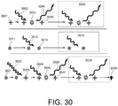
- FIG. 30 is a schematic diagram illustrating a PTOLs (e.g., a fluorescent molecule) stimulated by excitation radiation from a ground state into an excited state that emits a portion of the energy of the excited state into a fluorescence radiation photon.
- a PTOLs e.g., a fluorescent molecule
- FIG. 31 is a schematic diagram illustration excitation radiation that can excite an isolated emitter into an excited state.
- FIG. 32 is a schematic diagram illustrating how when weak intensity activation radiation bathes closely spaced PTOLs a small, statistically-sampled fraction of all the PTOLs that absorbs the activation radiation can be converted into a state that can be excited by excitation radiation.
- FIG. 33 is a schematic diagram illustrating how multiple sub-diffractive resolution images in two spatial dimensions, x and y, of individual PTOLs in a sample can be generated, and then the multiple images can be combined to generate a sub-diffraction limited resolution image of an x-y plane of the sample.
- FIG. 34 is a flow chart of a process for creating an image of a sample containing multiple relatively densely-located PTOLs.
- FIG. 35 is a schematic view of a system that can be used to implement the techniques described herein.
- This description discloses microscopy and imaging apparatus, systems, methods and techniques, which enable a light sheet or pencil beam to have a length that can be decoupled from its thickness, thus allowing the illumination of large fields of view (e.g., tens or even hundreds of microns) across a plane having a thickness on the order of, or smaller than, the depth of focus of the imaging objective by using illumination beams having a cross-sectional field distribution that is similar to a Bessel function.
- Such illumination beams can be known as Bessel beams.
- Bessel beams are created by focusing light, not in a continuum of azimuthal directions across a cone, as is customary, but rather at a single azimuthal angle or range of azimuthal angles with respect to the axis of the focusing element. Bessel beams can overcome the limitations of the diffraction relationship shown in FIG. 2 , because the relationship shown in FIG. 2 is only valid for lenses (cylindrical or objectives) that are uniformly illuminated.
- FIG. 3 is a schematic diagram of a Bessel beam formed by an axicon 300 .
- the axicon 300 is a conical optical element, which, when illuminated by an incoming plane wave 302 having an approximately-Gaussian intensity distribution in directions transverse to the beam axis, can form a Bessel beam 304 in a beam that exits the axicon.
- FIG. 4 is a schematic diagram of a Bessel beam 400 formed by an annular apodization mask 402 , where the annular mask 402 is illuminated to create a thin annulus of light at the back focal plane of a conventional lens 404 .
- the mask 402 is separated from the lens 404 by the focal length, f.
- An angle, ⁇ can be defined as the inverse tangent of half the distance, d, from the center of the annular ring to a point within the ring divided by the focal length, where d o can be used to denote the minimum diameter of the annular ring.
- d can be used to denote the minimum diameter of the annular ring.
- the axial wavevectors K z of all rays converging to the focus are the same, and hence there is no variation of the beam along this direction.
- the finite diameter of the axicon 300 or the finite width, ⁇ d, of the annular ring in the apodization mask 402 restricts the Bessel beam to a finite length.
- the optical system of the annular apodization mask 402 and the lens 404 can be characterized by a minimum and maximum numerical aperture, where the maximum numerical aperture is proportional to d o + ⁇ d, and the minimum numerical aperture is proportional to d o .
- different optical elements, other than an axicon or an apodization mask can be used to create an annulus of light.
- a binary phase mask or a programmable spatial light modulator can be used to create the annulus of light.
- FIG. 5 is a schematic diagram of a system 500 for Bessel beam light sheet microscopy.
- a light source 502 emits a light beam 504 that strikes an annular apodization mask 506 .
- An annulus of excitation light 508 illuminates the back focal plane of microscope objective 510 to create an elongated Bessel beam 512 of light in a sample 514 .
- FIG. 6A which shows a plot of the intensity profile of a Bessel beam
- FIG. 6B which shows a plot of the intensity profile of a conventional beam.
- Y is along the axis of the propagation direction of the beam
- X is the direction of the excitation polarization (when linearly polarized light is used)
- Z is along the axis of detection optics objective 522 and is orthogonal to X and Y.
- FIG. 7A is a plot of the intensity profile of a Bessel beam of FIG. 6A in the directions transverse to the propagation direction of the beam
- FIG. 7B is a plot of the Gaussian intensity profile of the conventional beam of FIG. 7A in the directions transverse to the propagation direction of the beam.
- annular illumination across a small range of angles results in a Bessel-like beam approximately 50 wavelengths ⁇ long in the Y direction, or roughly the same length obtained by conventional illumination using a plane wave having a Gaussian transverse intensity profile that is focused by a lens into an illumination beam having a cone half-angle of 12 degrees, as seen in FIG. 6 b .
- the thickness of the Bessel beam is much narrower than the thickness of the conventional beam, yielding a much thinner sheet of excitation when scanned across a plane.
- FIG. 8A is a plot of intensity profile in the YZ directions of a Bessel beam generated from an annular mask having a thinner annulus than is used to generate the intensity profile of the Bessel-like beam of FIG. 6A
- FIG. 8B is a plot of the transverse intensity profile for the beam in the XZ directions.
- annular illumination across a small range of angles results in in the YZ intensity profile of the Bessel-like beam shown in FIG.
- the Bessel-like beam has a length of approximately 100 wavelengths in the Y direction.
- the transverse intensity profile of the longer Bessel beam is relatively unchanged compared with shorter Bessel beam, as can be seen from a comparison of FIG. 7A and FIG. 8B , and the thickness of the beam is not significantly greater than the thickness of the beam whose intensity profile is shown in FIG. 6A .
- the usual approach of lengthening the beam by reducing the NA results in an unavoidably larger diffraction limited cross-section, roughly in accordance with Table 1.
- FIG. 9A is a schematic diagram of another system 900 for implementing Bessel beam light sheet microscopy.
- Collimated light 901 such as a laser beam having a Gaussian intensity profile, is reflected from first galvanometer-type mirror 902 and then imaged by relay lens pair 903 and 904 onto a second galvanometer-type mirror 905 positioned at a point optically conjugate to the first galvanometer-type mirror 902 .
- a second lens pair 906 and 907 then relays the light to annular apodization mask 908 conjugate with the second galvanometer-type mirror 905 .
- the annular light beam transmitted through this mask 908 is then relayed by a third lens pair 910 and 911 onto a conjugate plane coincident with the back focal plane of excitation objective 912 . Finally, the annular light is focused by objective 912 to form a Bessel-like beam 913 that is used to provide excitation light to a specimen.
- the rotational axis of galvanometer mirror 902 is positioned such that tilting this galvanometer-type mirror 902 causes the Bessel-like beam 913 to sweep across the focal plane of detection objective 915 (i.e., in the X direction), whose axis is orthogonal to (or whose axis has an orthogonal component to) the axis of the excitation objective 912 .
- the signal light 914 can be directed by detection optics, including the detection objective 915 , to a detection camera 917 .
- the galvanometers-type mirrors 902 , 905 can provide sweep rates of up to about 2 kHz, and with resonant galvanometer-type mirrors (e.g., Electro-Optical Products Corp, model SC-30) sweep rates can exceed 30 kHz. Extremely high frame rate imaging is then possible when the system is used in conjunction with a high frame rate detection camera (e.g., 500 frames/sec with an Andor iXon+DU-860 EMCCD, or >20,000 frames/sec with a Photron Fastcam SA-1 CMOS camera coupled to a Hamamatsu C10880-03 image intensifier/image booster).
- a high frame rate detection camera e.g., 500 frames/sec with an Andor iXon+DU-860 EMCCD, or >20,000 frames/sec with a Photron Fastcam SA-1 CMOS camera coupled to a Hamamatsu C10880-03 image intensifier/image booster.
- the rotational axis of the galvanometer mirror 905 is positioned such that tilting of this mirror causes Bessel-like beam 913 to translate along the axis of detection objective 915 .
- This mirror causes Bessel-like beam 913 to translate along the axis of detection objective 915 .
- either detection objective 915 In order to image each plane in focus, either detection objective 915 must be moved synchronously with the motion of the Bessel beam 913 imparted by the tilt of galvanometer-type mirror 905 (such as with a piezoelectric transducer (e.g., Physik Instrumente P-726)), or else the effective plane of focus of the detection objective 915 must be altered, such as by using a second objective to create a perfect image of the sample.
- the second galvanometer 905 and relay lenses 906 and 907 can be removed from the system shown in FIG.
- AOTF acousto-optical tunable filter
- the system in FIG. 9A is typically quite wasteful of the energy in light beam 901 , because most of this light is blocked by apodization mask 908 .
- a diffractive optical element such as a binary phase mask or spatial light modulator and a collimating lens can be used to create an approximately annular light beam prior to more exact definition of this beam and removal of higher diffractive orders by the apodization mask 908 .
- signal light 914 received by detection objective 915 can be transmitted through relay lenses 920 , 922 and reflected off a galvanometer-type mirror 924 and then transmitted through relay lenses 926 and 928 and focused by a tube lens 930 onto a detector 932 .
- An aperture mask (e.g., an adjustable slit) 934 can be placed at a focal plane of lens 926 , and the when the mask defines a slit the width of the slit 934 can be selected to block signal light from positions in the sample corresponding to side lobes of the Bessel-like beam illumination light, while passing signal light from positions in the sample corresponding to the central peak of the Bessel-like beam illumination light.
- the galvanometer-type mirror 924 can be rotated in conjunction with galvanometer-type mirror 902 , so that when the Bessel-like beam is scanned in the X direction within the sample signal light from different positions within the sample passes through the slit 934 .
- Bessel-like beams include excitation intensity in rings other than the central excitation maximum, which are evident in FIGS. 7A and 8B , and substantial energy resides in the side lobes of a Bessel-like beam. Indeed, for an ideal Bessel beam of infinite extent, each side lobe contains energy equal to that in the central peak. Also, for an ideal Bessel beam, the ratio of the Rayleigh length of the beam to the minimum waist size of the beam is infinite.
- each row indicates the maximum and minimum numerical aperture of the annular ring of the mask.
- the maximum numerical aperture is 0.80, and the minimum numerical aperture is 0.76.
- the maximum numerical aperture is 0.60, and the minimum numerical aperture is 0.58.
- the maximum numerical aperture is 0.53 and the minimum numerical aperture is 0.51.
- the maximum numerical aperture is 0.40, and the minimum numerical aperture is 0.38.
- the maximum numerical aperture is 0.20, and the minimum numerical aperture is 0.18.
- the intensity profile shown in FIG. 11A is representative of a Bessel-like beam formed from an annular apodization mask that generates an annulus of 488 nm light at a rear pupil of an excitation objective, where the annulus has a maximum numerical aperture of 0.60 and a minimum numerical aperture of 0.58.
- FIG. 12B shows plots of the axial intensity profiles (i.e., in the Y direction) of the beams that are swept. For each of the beams whose intensity profiles are plotted in FIG. 12A and FIG. 12B , the maximum numerical aperture is 0.60.
- a beam with an intensity profile 1202 has a minimum numerical aperture equal to 0.58.
- a beam with an intensity profile 1204 has a minimum numerical aperture equal to 0.56.
- a beam with an intensity profile 1206 has a minimum numerical aperture people equal to 0.52.
- the beam with an intensity profile 1208 has a minimum numerical aperture equal to 0.45.
- a beam with an intensity profile 1210 has a minimum numerical aperture equal to 0.30.
- the different apodization masks can have open regions with different widths, ⁇ d.
- a comparison of the plots in FIG. 12A and FIG. 12B shows the profiles of the beam changing from a profile that best approximates that of a lowest order (J 0 ) Bessel function (plot 1202 ) to a Gaussian profile ( 1212 ).
- This comparison indicates that the deleterious effect of the side lobes can be reduced by using a beam having a profile that is not substantially similar to that of a Bessel function, at the expense of having a beam with a shorter axial length.
- the selected beam can have a ratio of a Rayleigh length, z R to a minimum beam waist, w o , of more than 2 ⁇ w o / ⁇ and less than 100 ⁇ w o / ⁇ .
- the selected beam can have a non-zero ratio of a minimum numerical aperture to a maximum numerical aperture of less than 0.95.
- the selected beam can have a non-zero ratio of a minimum numerical aperture to a maximum numerical aperture of less than 0.9. In another implementation, the selected beam can have a ratio of a minimum numerical aperture to a maximum numerical aperture of less than 0.95 and greater than 0.80. In another implementation, the selected beam can have a non-zero ratio of a minimum numerical aperture to a maximum numerical aperture of less than 0.9. In another implementation, the selected beam can have a ratio of a minimum numerical aperture to a maximum numerical aperture of less than 0.95 and greater than 0.80. In another implementation, the selected beam can have a ratio of energy in a first side lobe of the beam to energy in the central lobe of the beam of less than 0.5.
- the length of the beam 516 that is necessary to image a specimen can be reduced by tilting a cover slip that supports the specimen with respect to the direction of the incoming beam 516 .
- a cover slip that supports the specimen with respect to the direction of the incoming beam 516 .
- the beam 516 would have to be 50 ⁇ m long to span the specimen.
- the plane of the cover slip at a 45° angle to the direction of the incoming beam 516 , then the beam would only need to be 5 ⁇ m ⁇ 2 long to span the sample.
- the beam 516 can be scanned in the X direction by tilting the galvanometer-type mirror 902 , and can be scanned in the Z direction either by introducing a third galvanometer (not shown) and a third pair of relay lenses (not shown) into the system 900 shown in FIG.
- Another approach to isolate the central peak fluorescence from that generated in the side lobes is to exclude the latter via confocal filtering with a virtual slit.
- the detector includes a plurality of individual detector elements, only those elements of the detector which an image the portion of the sample that is illuminated by the central lobe of the illumination beam can be activated to record information that is used to generate an image, while the individual detector elements upon which an image of the portion of the sample that is illuminated by side lobes of the illumination beam are not activated, such that they do not record information that is used to generate an image.
- FIG. 13A is a schematic diagram of a surface of a detector having a two-dimensional array of individual detector elements in the XY plane.
- FIG. 13A is a schematic diagram of a surface of a detector having a two-dimensional array of individual detector elements in the XY plane.
- FIG. 13B is a schematic diagram of “combs” of multiple Bessel-like excitation beams that can be created in a given Z plane.
- a comb of beams can be created by inserting a diffractive optical element (DOE, not shown) in the beam path between the light source and the galvanometer-type mirrors 902 , 905 , where the DOE diffracts a plurality of beams at different angles from the DOE, which end up being parallel to and spatially shifted from each other within the specimen.
- DOE diffractive optical element
- the spacing in the X direction between different beams of the comb is greater than the width of the fluorescence band generated by the side lobes of the beams. This allows information to be recorded simultaneously from rows of individual detector elements corresponding to the centers of the different beams of the comb, without the side lobes of neighboring beams interfering with the recorded signal for a particular beam.
- a comb of beams that illuminate a plane of a specimen 1308 can include the beams A 1 , B 1 , C 1 , D 1 , and E 1 , where the beams are separated by distances great enough so that side lobes of one beam in the comb do not overlap with a central portion of a neighboring beam.
- multiple “stripes” of an image can be simultaneously recorded. This process is then repeated, with additional images collected as the comb of Bessel-like illumination beams is translated in discrete steps having a width that corresponds to the spacing in the X direction between individual detector elements until all “stripes” of the final image have been recorded.
- the beams can be moved to new positions of A 2 , B 2 , C 2 , D 2 , and E 2 , where the spacing between the positions A 1 and A 2 , the spacing between positions B 1 and B 2 , etc. corresponds to the spacing between neighboring individual detector elements in the detector.
- fluorescence light from the beam position C 1 could be detected at a detector element 1302
- fluorescence light from the beam position C 2 can be detected at individual detector elements 1304 .
- the image is then digitally constructed from the information in all of the different stripes of the image.
- An acousto-optical tunable filter (AOTF) 918 can be used to block all excitation light from reaching the specimen between steps.
- AOTF acousto-optical tunable filter
- SI structured illumination
- I is an intensity at a point in the image
- n is an index value indicating an image from which I n is taken. Equation (1) is but one example of a linear combination of the individual images that will remove the weakly modulated out-of-focus component and retain the strongly modulated information near the focal plane.
- the beam may not be swept continuously, but rather can be moved in discrete steps to create a pattern of illumination light from which an image I n can be generated.
- the stepping period is larger than or approximately equal to the minimum period of ⁇ /2NA Bessel max required to produce a resolvable grating, but smaller than or approximately equal to ⁇ /NA Bessel max , the imposed pattern of illumination light contains a single harmonic, as required for the three-image, three-phase SI algorithm.
- the Bessel-like beam 913 can be moved across the X direction in discrete steps having a period greater than or approximately equal to ⁇ /2NA Bessel max and less than or approximately equal to ⁇ /NA Bessel max by controlling the position of the galvanometer-type mirror 902 , and detection light can be received and signals corresponding to the detected light can be recorded by the detector 917 when the beam 913 is in each of the positions. While the galvanometer-type mirror is being moved from one position to the next position, the illumination light can be blocked from reaching the sample by the AOTF. In this manner, an image I 1 can be generated from the detected light that is received when the illumination beam 913 is at each of its different positions.
- FIG. 14A shows theoretical and experimental structured illumination patterns that can be created with a 488 nm light Bessel-like beam having a maximum numerical aperture of 0.60 and the minimum numerical aperture of 0.58, that is moved across the X direction in discrete steps.
- the leftmost column of figures shows theoretical patterns of the point spread functions of the excitation light produced by stepping the beam across the X direction in discrete steps.
- the period the pattern (i.e., the spacing between successive positions of the center of the Bessel-like being as the beam is stepped in the X direction) is 0.45 ⁇ m.
- the period of the pattern In the second row, the period of the pattern is 0.60 ⁇ m.
- the period of the pattern In the third row the period of the pattern is 0.80 ⁇ m.
- a comb of multiple Bessel-like beams which are spaced by more than the width of the fringes of the beams in the comb, can be used to illuminate the specimen simultaneously, and then the comb of beams can be stepped in the X direction using the step size described above, so that different stripes of the specimen can be imaged in parallel and then an image of the specimen can be constructed from the multiple stripes.
- MTF excitation modulation transfer function
- Somewhat more energy can be transferred to the side bands using single harmonic excitation having a period far beyond the ⁇ /2NA detect max Abbe limit, but at the expense of proportionally poorer optical sectioning capability.
- An alternative that can better retain both signal and axial resolution is to create a multi-harmonic excitation pattern by stepping the beam at a fundamental period larger than ⁇ /NA Bessel max , as seen in FIG. 15A , which shows theoretical and experimental higher-order harmonic structured illumination patterns that can be created with Bessel-like beams having a maximum numerical aperture of 0.60 and the minimum vertical aperture of 0.58, which are created with 488 nm light.
- Eq. (1) is again used, except with N ⁇ H+2 images, each with the pattern phase shifted by 2 ⁇ /N relative to its neighbors.
- FIG. 15B shows theoretical and experimental modulation transfer functions (MTFs) in reciprocal space, which correspond to the point spread functions shown in the two left-most columns of FIG. 15A .
- MTFs modulation transfer functions
- both single-harmonic and multi-harmonic SI modes still generate some excitation beyond the focal plane, and are thus not optimally efficient in their use of the photon budget.
- Both these issues can be addressed using two-photon excitation (TPE), which suppresses the Bessel side lobes sufficiently such that a thin light sheet can be obtained even with a continuously swept beam.
- TPE two-photon excitation
- high axial resolution and minimal out-of-focus excitation is achieved in fixed and living cells with only a single image per plane.
- Some additional improvement is also possible with TPE-SI, but the faster TPE sheet mode can be preferred for live cell imaging.
- TPE TPE
- CARS coherent anti-Stokes Raman scattering
- the improved confinement of the excitation light to the vicinity of the focal plane of the detection objective made possible by Bessel beam plane illumination leads to improved resolution in the axial direction (i.e., in the direction along the axis of the detection objective) and reduced photobleaching and phototoxicity, thereby enabling extended observations of living cells with isotropic resolution at high volumetric frame rates.
- extended imaging of the endoplasmic reticulum in a live human osteosarcoma cell (U2OS cell line) in the linear multi-harmonic SI mode was performed.
- U2OS cell line live human osteosarcoma cell
- Such ruffles can surround and engulf extracellular fluid to create large intracellular vacuoles, a process known as macropinocytosis, which was directly demonstrated using the techniques described herein.
- the visualization of these processes in four dimensional spatiotemporal detail (0.12 ⁇ 0.12 ⁇ 0.15 ⁇ m ⁇ 12.3 sec stack interval) across 15 minutes cannot currently be achieved with other fluorescence microscopy techniques.
- CMOS camera 125 MHz, Hamamatsu Orca Flash 2.8
- a third galvanometer-type mirror that can be tilted can be placed at a plane conjugate to the rear pupil of the detection objective and used to tile several image planes across the width of the detector, which were then are read out in parallel.
- FIG. 16 shows a system 1600 with a mirror placed at a plane that is conjugate to the detection objective between the detection objective and the detector.
- detection light collected by detection objective 1602 can be focused by a tube lens 1604 to form an image at the plane of an adjustable slit 1606 .
- the image cropped by the adjustable slit 1606 is reimaged by relay lenses 1608 onto a high-speed detection camera 1610 .
- a galvanometer-type mirror 1612 is placed the plane between the relay lenses 1608 that is conjugate to the back focal plane of the detection objective 1612 . By changing the angle of galvanometer-type mirror, multiple images can be exposed across the surface of the detection camera 1610 and then read out in parallel to exploit the full speed of the detection camera 1610 .
- Three-dimensional live cell imaging can be performed with Bessel-like beans with the use of fluorescent proteins to highlight selected portions of a specimen.
- a key aspect of fluorescent proteins (FPs) is that their spectral diversity permits investigation of the dynamic interactions between multiple proteins in the same living cell. For example, after transfection with mEmerald/MAP4 and tdTomato/H2B, microtubules in a pair of U2OS cells surrounding their respective nuclei, were imaged in the linear, nine-phase multi-harmonic SI mode. Nevertheless, although many vectors are available for linear imaging, the need for N frames of different phase per image plane can limits the use of SI with Bessel-like beams to processes which evolve on a scale that matches the time required to collect frames at the desired spatial resolution.
- the TPE sheet mode can be used for imaging multiple proteins exhibiting faster dynamics.
- the 3D isotropic resolution of the Bessel TPE sheet mode permits multiple proteins tagged with the same FP to be imaged simultaneously, as long as they are known a priori to be spatially segregated.
- Bessel beam plane illumination microscopy techniques offer 3D isotropic resolution down to ⁇ 0.3 ⁇ m, imaging speeds of nearly 200 planes/sec, and the ability, in TPE mode, to acquire hundreds of 3D data volumes from single living cells encompassing tens of thousands of image frames. Nevertheless, additional improvements are possible.
- substantially greater light collection making still better use of the photon budget is obtained by using a detection objective with a numerical aperture of 1.0 or greater.
- mechanical constraints would thereby force the use of an excitation objective with a numerical aperture of less than 0.8 thus lead to a somewhat anisotropic point spread function (PSF)
- the volumetric resolution would remain similar, since the slight loss of axial resolution would be offset by the corresponding transverse gain.
- An alternative would be to use the algorithms of 3D superresolution SI, which assign the sample spatial frequencies down-modulated by all bands of the excitation to their appropriate positions in an expanded frequency space. By doing so, shorter exposure times and fewer phases are needed to record images of acceptable SNR, making linear Bessel SI a more viable option for high speed multicolor imaging.
- resolution can be extended to the sum of the excitation and detection MTF supports in each direction—an argument in favor of using three mutually orthogonal objectives. Indeed, the marriage of Bessel beam plane illumination and 3D superresolution SI permits the latter to be applied to thicker, more densely fluorescent specimens than the conventional widefield approach, while more efficiently using the photon budget.
- Superresolution SI can be performed by extending the structured illumination techniques described above with respect to FIG. 14 and FIG. 15 .
- illuminating the sample with a structured illumination pattern normally inaccessible high-resolution information in an image of a sample can be made accessible in the form of Moire fringes.
- a series of such images can be processed to extract this high-frequency information and to generate reconstruction of the image with improved resolution compared to the diffraction limited resolution.
- one of the patterns can be the unknown sample structure, for example, the unknown spatial distribution of regions of the sample that receive illumination light and that emit signal light—and the other pattern can be the purposely structured pattern of excitation light that is written in the form of parallel Bessel-like beams. Because the amount of signal light emitted from a point in the sample is proportional to the product of the local excitation light intensity and the relevant structure of the sample, the observed signal light image that is detected by the detector will show the beat pattern of the overlap of the two underlying patterns. Because the beat pattern can be coarser than those of the underlying patterns, and because the illumination pattern of the Bessel-like beams is known, the information in the beat pattern can be used to determine the normally unresolvable high-resolution information about the sample.
- the patterns shown in FIG. 17A can be Fourier transformed into reciprocal space.
- the Fourier transform of the structure of a sample that is imaged by an a convention widefield optical system is constrained by the Abbe resolution limit would be represented by a circle having a radius of 2NA/ ⁇ , as shown in FIG. 17B , where the low resolution components of the sample are close to the origin, and the high-resolution components are close to the edge of the circle.
- the Fourier transform of a 2D illumination pattern that consists of a sinusoidal variation in the illumination light in one dimension and having a period equal to the diffraction limit of the optical system has three non-zero points that lie on the circle shown in FIG. 17C .
- the resulting beat pattern between the specimen structure and the illumination structure represents information that has changed position in reciprocal space, such that the observable region of the sample in physical space then contains new high-frequency information represented by the two regions and FIG. 17D that are offset from the origin.
- the regions of the offset circles in FIG. 17D that fall outside the central circle represent new information that is not accessible with a conventional eidefield technique.
- FIG. 17E When a sequence of such images is obtained using structured excitation radiation that is oriented in different directions multiple circles that lie outside the central circle are produced, as shown in FIG. 17E . From this plurality of images, information can be recovered from an area that can be twice the size of the normally observable region, to increase the lateral resolution by up to a factor of two is compared with widefield techniques.
- N images can be recorded with the spatial phase of the illumination pattern between each image shifted by ⁇ /N in the X direction, where ⁇ is the spatial period of the pattern and N is the number of harmonics in reciprocal space. Then, a Fourier transform can be performed on each of the N images, and the reciprocal space images can moved to their true positions in reciprocal space, combined through a weighted-average in reciprocal space, and then the weight-averaged reciprocal space image can be re-transformed to real space to provide an image of the sample.
- a superresolution image of the sample can be obtained, where the resolution of the image in both the X and Z directions can be enhanced over the Abbe diffraction limited resolution.
- the resolution enhancement in the X direction can be up to a factor of two when the NA of the structured excitation and the NA of the detection are the same.
- the excitation lens NA is usually lower than that of the detection lens, so the extension beyond the Abbe limit is usually less than a factor of two but more than a factor of one.
- the resolution improvement can be better than a factor of two, since the transverse Z resolution of the excitation can exceed the transverse Z resolution of the detection.
- more than one excitation objective can be used to provide a structured illumination pattern to the sample, where the different excitation objectives can be oriented in different directions, so that super resolution of the sample can be obtained in the directions transverse to the Bessel-like beams of each of the orientation patterns.
- a first excitation objective can be oriented with its axis along the Y direction (as described above) and can illuminate the sample with an illumination pattern of Bessel-like beams that provides a superresolution image of the sample in the X and Z directions
- a second excitation objective can be oriented with its axis along the X direction and can illuminate the sample with an illumination pattern of Bessel-like beams that provides a superresolution image of the sample in the Y and Z directions.
- the superresolution information that can be derived from illumination patterns from the different excitation objectives can be combined to yield extended resolution in all three directions.
- highly inclined, objective-coupled sheet illumination has been used to image single molecules in thicker regions of the cell where autofluorescence and out-of-focus excitation would be otherwise prohibitive under widefield illumination.
- Bessel beam plane illumination only in-focus molecules would be excited, while out-of-focus ones would not be prematurely bleached. As such, it would be well suited to live cell 3D particle tracking and fixed cell photoactivated localization microscopy.
- the TPE sheet mode may be equally well suited to the imaging of large, multicellular specimens, since it combines the self-reconstructing property of Bessel beams with the improved depth penetration in scattering media characteristic of TPE.
- the TPE sheet mode may be equally well suited to the imaging of large, multicellular specimens, since it combines the self-reconstructing property of Bessel beams with the improved depth penetration in scattering media characteristic of TPE.
- the TPE sheet mode may be equally well suited to the imaging of large, multicellular specimens, since it combines the self-reconstructing property of Bessel beams with the improved depth penetration in scattering media characteristic of TPE.
- 3D anatomical mapping with isotropic resolution at high frame rates it might be fruitfully applied to the in vivo imaging of activity in populations of neurons.
- additional spatial frequencies are introduced to images generated from detected light that is emitted from the sample, and the additional spatial frequencies can provide additional information that may be exploited to enhance the resolution of a final image of the sample generated through the super resolution structured illumination techniques described herein
- FIG. 18A is a schematic diagram of a system 1800 for generating and providing an array of Bessel-like excitation beams to a sample, similar to the comb of beams show in FIG. 13B , and for imaging the light emitted from the sample due to interaction between the Bessel-like beams and the sample.
- a light source 1802 e.g., a laser
- can produce coherent, collimated light such as a beam having a Gaussian intensity profile, which can be reflected from first galvanometer-type mirror 1804 .
- the mirror 1804 can be controlled by a fast motor 1806 that is used to rotate the mirror and steer the beam in the X direction.
- After the beam is reflected from the mirror 1804 it is imaged by relay lens pair 1808 and 1810 onto a second galvanometer-type mirror 1812 positioned at a point optically conjugate to the first galvanometer-type mirror 1804 .
- the mirror 1812 can be controlled by a fast motor 1814 that is used to rotate the mirror and steer the beam in the Z direction.
- a second lens pair 1816 and 1818 then can relay the light to a diffractive optical element (DOE) 1824 located just in front of an annular apodization mask (AM) 1822 that is conjugate with the second galvanometer-type mirror 1812 .
- the DOE 1820 can be, for example, a holographic diffractive optical element, that creates, in the far field from the DOE, a fan of Gaussian beams. In some implementations, the DOE can create a fan of seven beams.
- the apodization mask 1822 located just after the DOE 1820 , can be used in combination with the DOE to generate an array of Bessel-like beams in the sample 1840 .
- the annular light beams transmitted through the AM 1822 are relayed by a third lens pair 1826 and 1828 onto a conjugate plane coincident with the back focal plane of excitation objective 1830 . Finally, the annular light beams are focused by the objective 1830 to form a fan of Bessel-like beam s that are used to provide excitation light to the sample 1840 .
- the sample 1840 can be placed in an enclosed sample chamber 1832 that can be filled with aqueous media and that can be temperature controlled.
- Signal light emitted from the sample can be collimated by a detection objective 1834 and focused by a tube lens 1836 onto a position sensitive detector 1838 .
- the signal light emitted from the sample can be generated through a non-linear signal generation process. For example, in one implementation, the signal light may be generated through a two-photon process, such that the signal light has a wavelength that is one half the wavelength of the excitation light of the Bessel-like beams.
- FIGS. 18B and 18C are example diagrams showing an array of substantially parallel Bessel-like beams produced by the system 1800 .
- FIG. 18B shows the array of beams in the X-Y plane
- FIG. 18C shows the array of beams in the X-Z plane, although FIG. 18C shows only five of the seven Bessel-like beams.
- a diffractive optical element that produces seven beams in combination with the other beam-forming optics of system 1800 , including the apodization mask 1822 and the excitation objective 1830 , can create the array of seven Bessel-like beams shown in FIGS. 18B and 18C . As shown in FIGS.
- the beams for particular parameters and configurations of the beam-forming optics of system 1800 , including the dimensions of the apodization mask, the numerical aperture of the excitation objective 1830 , etc.
- the Bessel-like beams that are produced in the sample can extend over a length of approximately 10 ⁇ m, and can have central lobes with diameters on the order of 1 ⁇ m.
- an array having a plurality of beams can be stepped across the sample to create an incoherent structured illumination pattern over a given field of view faster than one beam can be stepped.
- the rotational axis of galvanometer mirror 1804 can be positioned such that tilting this galvanometer-type mirror 1804 causes the array of Bessel-like beams to sweep across the focal plane of detection objective 1834 (i.e., in the X direction), whose axis is orthogonal to (or whose axis has an orthogonal component to) the axis of the excitation objective 1830 .
- the array of Bessel-like beams can be swept in the X direction to produce a thin sheet of light in a plane.
- the signal light emitted from the sample 1840 can be directed by detection optics, including the detection objective 1834 , to a detector 1838 .
- the galvanometers-type mirrors 1804 , 1812 can provide sweep rates of up to about 2 kHz, and with resonant galvanometer-type mirrors (e.g., Electro-Optical Products Corp, model SC-30) sweep rates can exceed 30 kHz. Extremely high frame rate imaging is then possible when the system is used in conjunction with a high frame rate detection camera.
- the rotational axis of the galvanometer mirror 1812 can be positioned such that tilting of this mirror causes the array of Bessel-like beams to translate along the Z axis of detection objective 1834 .
- different planes within a specimen can be accessed by the Bessel beam, and a three dimensional (3D) image of the specimen can be constructed, with much higher axial resolution than in conventional light sheet microscopy, due to the much narrower sheet of excitation afforded by array of Bessel-like excitation.
- either detection objective 1834 In order to image each plane in focus, either detection objective 1834 must be moved synchronously with the motion of the array of Bessel-like beams imparted by the tilt of galvanometer-type mirror 1812 (such as with a piezoelectric transducer), or else the effective plane of focus of the detection objective 1834 must be altered, such as by using a second objective to create a perfect image of the sample.
- the excitation plane and the detection plane can remain fixed and the sample can be moved through the planes, for example, by using a piezoelectric transducer to move the sample through the beam to cover different z planes. For relatively flat samples, this allows the use of a shorter Bessel-like beams in the Y-direction with less energy in the side-lobes.
- the plurality of Bessel-like beams can lie in a plane within the sample and can be equally spaced from neighboring beams, such that the plurality of beams form a pattern in the plane having a spatial period, 158 .
- the array of beams can be scanned in a direction perpendicular to their propagation direction (e.g., in the X direction).
- the array of beams can be scanned in a series of discrete steps. For example, the array of beams can be scanned from its original position in N- 1 discrete steps, where N is an integer, and the steps can have a length of (N- 1 ) ⁇ /N.
- Images of the sample can be recorded based on light emitted from the sample when the array of Bessel-like beams is in each of the N different positions within the sample (i.e., in the original position and in the N- 1 scanned positions). Then, a final image of the sample can be generated through a linear combination of the N individual images of the sample. For example, the linear combination of the different images can be created according to
- I final is an intensity of the final image at a particular position within the sample
- n is an index variable corresponding to the different individual images that are generated
- In is an intensity of the particular position within the sample in the nth individual image.
- the array of the Bessel-like beams can be spatially dithered (i.e., rapidly changed in a periodic manner) at a dither frequency back and forth in the plane of the array of beams.
- the galvanometer-type mirror 1804 can be tilted back and forth to dither the spatial position of the array of Bessel-like beams.
- the array of Bessel-like beams can be spatially dithered over a distance greater than or approximately equal to the spatial period, ⁇ , of the pattern of the array of Bessel-like beams.
- the Bessel-like beams can be moved in the plane at the array (e.g., along the X axis) at a substantially constant rate, so that the time-averaged intensity of light in the plane of the array is substantially constant.
- the inverse of the dither frequency is greater than the integration time of the detector 1838 , the excitation light provided by the array of Bessel-like beams in the sample can appear to the detector as a uniform sheet of excitation light.
- the system in FIG. 18A is typically quite wasteful of the energy in light beam 1801 , because most of this light is blocked by apodization mask 1808 .
- a diffractive optical element such as a binary phase mask or spatial light modulator and a collimating lens can be used to create an approximately annular light beam prior to more exact definition of this beam and removal of higher diffractive orders by the apodization mask 1808 .
- the different, substantially parallel Bessel-like beams that are produced from the light of the light source and the beam-forming optics shown in FIG. 18A can be created from a single source of coherent light, and the beam-forming optics can be held in stable positions, such that fixed phase relationships exist between the different substantially parallel Bessel-like beams in the sample.
- the different Bessel-like beams can be spaced apart from the other with the spacing that is great enough so that the light from neighboring Bessel beams does not interact substantially.
- Another technique to reduce the influence of the side lobes and to improve the Z-axis resolution of images obtained of a sample is to employ structured illumination using a coherent array of Bessel-like beams that are provided simultaneously to the sample, such that interference between the beams of the coherent array improves the Z-axis confinement of the plane of structured illumination that is used to provide excitation radiation to the sample.
- structured illumination plane One way to imagine the creation of such a structured illumination plane is to think of the plane being created by different beams that are spaced apart from their neighboring beams by distances small enough for neighboring beams to overlap and interfere with each other.
- FIG. 19 is a schematic diagram of another system 1900 for producing an array of Bessel-like beams in a sample.
- the light beam from the light source 1902 can be spatially expanded in the X direction by a pair of cylindrical lenses 1904 A, 1904 B and can be spatially reduced in the Z direction by a pair of cylindrical lenses 1906 A, 1906 B to produce a beam having an intensity profile that is wide in the X direction and narrow in the Z direction.
- the beam can pass through a beam splitter 1908 half-wave plate 1910 and then impinge on a wavefront modulating element (WME) 1912 that independently modulates individual portions of the entire wavefront.
- WME wavefront modulating element
- the insertion of the half-wave plate 1910 in the beam path can make the WME 1912 operate as a phase modulator of portions of the beam that strike the WME.
- the WME can include a liquid-crystal phase-only spatial light modulator.
- the WME can include a ferroelectric binary spatial light modulator.
- the WME 1912 can include a deformable mirror (e.g., a piston-tip-tilt mirror) or an array of micromirrors.
- the WME 1912 By controlling the WME 1912 (e.g., by control of the individual pixels of a spatial light modulator or individual mirrors within an array of micrometers or control of individual elements of a piston-tip-tilt mirror), the wavefront of the light reflected from the WME 1912 , and consequently the wavefront(s) of downstream beam(s) (e.g., beams in the sample 1946 ), can be controlled.
- the WME 1912 can be programmed to modulate the wavefront of the incoming light beam such that the outgoing light beam from the WME subsequently defines an array of coherent Bessel-like beams that overlap and interfere with each other to create a plane of structured illumination in the sample 1946 .
- the WME 1912 can be optically conjugated to the sample 1946 , so that modulations introduced by the WME can be propagated to the sample.
- the WME 1912 can be used to control the relative phases of individual beamlets (or portions of the incoming wavefront) that are reflected from the WME.
- the WME 1912 can be used to control the relative phases of individual portions of the wavefront that strike the WME 1912 and that then propagate into the sample 1946 .
- this relative phase control of individual portions of the reflected wave front can result in control of relative phases of individual Bessel-like beams in array of beams in the sample 1946 .
- the WME 1912 can include a spatial light modulator, and in some implementations the spatial light modulator can be a binary spatial light modulator, in which each pixel of the spatial light modulator can have one of two different states that affect the light modulated by the pixel. In some implementations, the WME 1912 can be used to scan the array of Bessel-like beams within the sample—either within the plane of the array or perpendicular to the plane (e.g. in the Z axis direction).
- An advantage of using a reflective spatial light modulator (SLM) as the WME is that, with a high number of pixels (e.g., 1024 ⁇ 1280 pixels), it can be readily divided into many subregions, and in part because the subregions are truly independent, and not mechanically coupled, as in a deformable mirror.
- SLM spatial light modulator
- the light reflected from the WME can be reflected by the beam splitter 1908 and reflected by mirrors 1914 , 1916 . Then, the light can be imaged by a lens 1918 onto an apodization mask 1920 that is conjugate to the rear pupil of the excitation objective 1942 .
- the apodization mask 1920 the light can be reflected off of a mirror 1922 , transmitted through relay lenses 1924 , 1926 , reflected off galvanometer mirror 1928 , mirror 1930 , transmitted through relay lenses 1932 , 1934 , reflected off galvanometer mirror 1936 , and transmitted through relay lenses 1938 , 1940 to the rear pupil plane of excitation objective 1942 . Then, the light can be focused by excitation objective 1942 onto the sample 1946 that is housed in chamber 1944 .
- Mirror 1928 can operate as a galvanometer-type mirror to translate the structured plane illumination in the X direction within the sample, and the mirror 1928 can be conjugated to the apodization mask 1920 by relay lenses 1924 , 1926 .
- Mirror 1936 can operate as a galvanometer-type mirror to translate the structured plane illumination in the Z direction within the sample, and the mirror 1936 can be conjugated to mirror 1928 by relay lenses 1932 , 1934 .
- the rear pupil plane of excitation objective 1942 can be conjugated to mirror 1936 by relay lenses 1938 and 1940 .
- the combination of lenses 1918 , 1924 , 1926 , 1932 , 1934 , 1938 , and 1940 as well as excitation objective 1942 then serve to conjugate WME 1912 to an excitation plane within the sample 1946 .
- the sample 1946 can be supported on a translation stage 1947 that can be used to translate the sample in space.
- the translation stage 1947 can translate the sample 1946 with respect to a beam of radiation that is provided to the sample, while the position of the beam remains fixed.
- Light emitted from the sample 1946 due to the interaction of the excitation light with the sample can be collected by the detection objective 1948 and then focused by lens 1950 onto a detector 1952 .
- Information collected by the detector 1952 can be sent to a computing device 1954 , which may include one or more processors and one or more memories.
- the computing device may process the information from the detector 1952 to create images of the sample 1946 based on the information provided by the detector 1952 .
- intersection point can occur at a position that is closer to the plane of the array than a diameter of the first side lobe of the Bessel-like beams.
- FIG. 20 is a flowchart of a process 2000 of determining a pattern to apply to a binary spatial light modulator, which will produce a coherent structured light sheet having a relatively low thickness in the Z direction over a sufficient length in the Y direction to image samples of interest.
- the complex electric field E b (x, z) of a single Bessel-like beam propagating in the Y direction into the sample is calculated (step 2002 ).
- the complex electric field is chosen based on a maximum NA to achieve a desired maximum X-Z spatial frequency and based on a minimum NA to achieve a desired beam length in the Y direction.
- the complex electric field E tot (x, z) of the structured light sheet that is formed by a coherent sum of a plurality of Bessel-like beams in a linear periodic array of Bessel-like beams can be calculated (step 2004 ).
- the total complex electric field of the array of beams can be expressed as:
- ⁇ is the phase difference between adjacent beams in the array
- T is the spatial period of the array of beams.
- ⁇ can be set equal to 0 or ⁇ (i.e., all beams can have the same phase, or beams can have alternating opposite phases).
- the field values having a magnitude lower than a threshold value, ⁇ can be set to zero (step 2010 ).
- E bound ( x,z ) where ⁇ ( ⁇ ) 1, for ⁇ >0and0 for ⁇ 0.
- FIGS. 21A-21F show a series of graphical illustrations of the process 2000, when the processes used to generate a thin array of structured excitation radiation is swept in the X direction to generate a plane of excitation illumination.
- FIG. 21A illustrates a cross-sectional profile in the X-Z plane of a Bessel like beam propagating in the Y direction. The particular cross section shown in FIG. 21A is for a Bessel-like beam having a maximum numerical aperture of 0.60 and a minimum numerical aperture of 0.54. Higher electric field strengths are shown by whiter regions in FIG. 21A .
- FIG. 21B illustrates the electric field, in the X-Z plane, of a structured light sheet formed by coherent sum of a linear, periodic array of Bessel-like beams that propagate in the Y direction.
- the individual Bessel-like beams have a maximum numerical aperture of 0.60 and a minimum numerical aperture is 0.54.
- the wavelength of the light is 488 nm, and the period of the array of beams is 0.90 ⁇ m, and the individual-beams of the array all have the same phase.
- Higher electric field strengths are shown by whiter regions in FIG. 21B .
- the lengths shown on the axes of all of the panels of FIGS. 21A-F are normalized the wavelength of light in the medium within the sample chamber 1944 .
- FIG. 21C illustrates the electric field, in the XZ plane, of the structured light sheet of FIG. 21B after a Gaussian envelope function has been applied to the field of the light sheet to bound the light sheet in the Z direction. Higher electric field strengths are shown by whiter regions.
- FIG. 21D illustrates the pattern of phase shifts applied to individual pixels of a binary spatial light modulator to generate the field shown in FIG. 21C . Pixels generating a phase shift of ⁇ are shown in black, and pixels generating a phase shift of zero are shown in white.
- FIG. 21D illustrates the pattern of phase shifts applied to individual pixels of a binary spatial light modulator to generate the field shown in FIG. 21C . Pixels generating a phase shift of ⁇ are shown in black, and pixels generating a phase shift of zero are shown in white.
- FIG. 21E illustrates the cross-sectional point spread function, in the X-Z plane, of the structured plane of excitation radiation that is produced in the sample by the coherent array of Bessel-like beams, which are generated by the pattern on the spatial light modulator shown in FIG. 21D . Higher light intensities are shown by whiter regions.
- FIG. 21F illustrates the excitation beam intensity that is produced in the sample when the array of Bessel-like beams is swept or dithered in the X direction. Higher intensities are shown by whiter regions.
- Changing the period of the array of the coherent Bessel-like beams can affect the overall electric field pattern resulting from the interference of the plurality of beams.
- the resulting electric field interference pattern can extend relatively more or less in the Z direction. This effect can be exploited to determine parameters of the coherent array that can be useful for generating images of the sample using super resolution structured illumination techniques as well as using a thin sheet of structured illumination that is swept in the X direction.
- FIGS. 22A-22F show a series graphical illustrations of the process 2000 , when the plane is used to generate an array of structured excitation radiation that is used to generate images of the sample using super resolution structured illumination techniques.
- FIG. 22A illustrates a cross-sectional profile in the X-Z plane of a Bessel like beam propagating in the Y direction.
- the particular cross section shown in FIG. 22A is identical to that of FIG. 21A and is for a Bessel-like beam having a maximum numerical aperture of 0.60 and a minimum numerical aperture of 0.54.
- the lengths shown on the axes of all of the panels of FIGS. 22A-22F are normalized the wavelength of light in the medium within the sample chamber 1944 .
- FIG. 22B illustrates the electric field, in the X-Z plane, of a structured light sheet formed by a coherent sum of a linear, periodic array of Bessel-like beams that propagate in the Y direction.
- the individual Bessel-like beams have a maximum numerical aperture of 0.60 and a minimum numerical aperture is 0.54.
- the wavelength of the light is 488 nm, and the period of the array of beams is 0.92 ⁇ m and the individual beams of the array all have the same phase.
- the period of the array illustrated in FIG. 22B is 0.02 ⁇ m longer than the period of the array illustrated in FIG. 21B .
- FIG. 22C illustrates the electric field, in the XZ plane, of the structured light sheet of FIG. 22B after a Gaussian envelope function has been applied to the field of the light sheet to bound the light sheet in the Z direction.
- the structured light sheets shown in FIGS. 22A-22F are to be used for super resolution structured illumination microscopy, in which it may be desirable to have the electric field extend further in the Z direction then when using the light sheet in a swept sheet mode, and therefore the envelope (or “bounding”) function used in FIG. 22C may be relatively more relaxed than the bounding function used in FIG. 21C .
- FIG. 22D illustrates the pattern of phase shifts applied to individual pixels of a binary spatial light modulator to generate the field shown in FIG. 22C . Pixels generating a phase shift of ⁇ are shown in black, and pixels generating a phase shift of zero are shown in white.
- FIG. 22E illustrates the cross-sectional point spread function, in the X-Z plane, of the structured plane of excitation radiation that is produced in the sample by the coherent array of Bessel-like beams, which are generated by the pattern on the spatial light modulator shown in FIG. 22D .
- FIG. 22F illustrates the modulation transfer function, which corresponds to the point spread functions shown in FIG. 22E . All of the MTFs are normalized to 4 ⁇ / ⁇ , where ⁇ is the wavelength of light in the medium within the sample chamber 1944 .
- the coherent superposition of a plurality of Bessel-like beams bears little resemblance to the electric field patterns and point spread function patterns of individual Bessel-like beams.
- changing the period of the array of beams causes large changes in optical properties of the optical lattices (e.g., the period, symmetry, and degree of bounding in the Z direction of the lattices) that result from interference between the beams of the array.
- the coherent superposition of an array of Bessel-like beams forms a spatially-structured plane of excitation radiation that can be used to excite optical labels within a sample, which then emit light that is detected and used to generate an image of the sample.
- the spatially-structured plane of excitation radiation can be swept in a direction parallel to the plane to generate a thin sheet of excitation radiation.
- the spatially-structured plane of excitation radiation can be translated in discrete steps in a direction parallel to the plane and emit light can be detected when the plane is in each of the different positions. Then, the light detected from the sample when the plane is in each of the different positions can be algorithmically combined to generate a super resolution image of the sample.
- FIGS. 23A-23F is a schematic diagram of the intensities of different modes of excitation radiation that is provided to the sample.
- FIG. 23A is a cross-sectional in the X-Z plane of a Bessel-like beam propagating in the Y direction. The particular cross section shown in FIG. 23A is for a Bessel-like beam having a wavelength of 488 nm and having a maximum numerical aperture of 0.60 and a minimum numerical aperture of 0.54. Higher intensities are shown by whiter regions.
- the Bessel-like beam of FIG. 23A is swept in the X direction, then the time-averaged intensities in the X-Z plane shown in FIG. 23B results.
- FIG. 23A is a cross-sectional in the X-Z plane of a Bessel-like beam propagating in the Y direction.
- the particular cross section shown in FIG. 23A is for a Bessel-like beam having a wavelength of 488 nm and having a maximum numerical aperture of 0.60 and a minimum numerical aperture
- FIG. 23C is a cross-sectional in the X-Z plane of a superposition of incoherent Bessel-like beams propagating in the Y direction, such as would occur if the single Bessel-like beam in FIG. 23A were moved in discrete steps.
- the pattern shown in FIG. 23C is for a 488 nm Bessel-like beam having a maximum numerical aperture of 0.60 and a minimum numerical aperture of 0.54, stepped in units of 0.90 ⁇ m.
- FIG. 23E is a cross-section in the X-Z plane of a superposition of coherent Bessel-like beams propagating in the Y direction.
- the pattern shown in FIG. 23E is for an array of 488 nm Bessel-like beams having a maximum numerical aperture of 0.60 and a minimum numerical aperture of 0.54, with individual beams of the array being spaced 0.90 ⁇ m from each other.
- the array of Bessel-like beams of FIG. 23E is swept or dithered in the X direction, then the time-averaged intensity in the X-Z plane shown in FIG. 23F results.
- FIG. 23B FIG. 23D , and FIG.
- the coherent array of Bessel-like beams can result in a light sheet that is more tightly confined in the Z direction that a light sheet that is produced by sweeping a single Bessel-like beams ( FIG. 23B ) or a light sheet that is produced by sweeping an incoherent array of Bessel-like beams ( FIG. 23D ).
- the coherent superposition of a plurality of Bessel-like beams forms a spatially-structured plane of excitation radiation.
- These patterns can be viewed as optical lattices that are created by interference within the sample between different beamlets of the beam that is modulated by the spatial light modulator 1912 shown in FIG. 19 and then enter the sample 1946 through the excitation objective 1942 . Therefore, in some implementations, a pattern can be applied to the WME 1912 that creates an optical lattice within the sample, which can be used to generate a spatially-structured plane of excitation radiation that can be used to generate images of the sample 1946 .
- FIG. 24 is a flowchart of a process 2400 of determining a pattern to apply to a binary spatial light modulator, which will produce an optical lattice within the sample, where the optical lattice can be used as a coherent structured light sheet having a relatively low thickness extent in the Z direction over a sufficient length in the Y direction to image samples of interest.
- the complex electric field E lattice (x, z) of a selected two-dimensional 2D optical lattice can be calculated (step 2402 ).
- the selected optical lattice can be, for example, a fundamental lattice, a sparse lattice, a composite lattice, or a maximally symmetric composite lattice, as described in U.S. Pat. No. 7,609,391, entitled “Optical Lattice Microscopy,” issued on Oct. 27, 2009, which is incorporated herein by reference.
- a maximally symmetric composite lattice can be selected to provide tight confinement of the excitation radiation in the Z direction when generating images of the sample using the swept sheet mode and to provide high spatial frequency components in the XZ plane when generating images of the sample using the super resolution, structured illumination mode.
- maximally symmetric composite hexagonal and square lattices can be used, because they can provide more wavevectors than lattices with other symmetry.
- the lattice can be rotated about the Y axis to a desired orientation (step 2404 ).
- a desired orientation For example, an orientation of the lattice in which lattice wavevectors lie along the X axis facilitates the construction of structured light sheets that are tightly confined in the Z direction.
- an optical lattice having a periodicity and orientation such that adjacent lines of the lattice maximum along the X direction are separated by more than the desired light sheet thickness in the Z direction can be useful when using the lattice to generate images of the sample with the swept sheet mode.
- the lines of lattice maximum along the X direction should be separated by less than the desired light sheet thickness when using the super resolution, structured illumination mode to generate images of the sample.
- ⁇ ) E bound ( x, z ) where ⁇ ( ⁇ ) 1, for ⁇ >0 and 0 for ⁇ 0.
- FIGS. 25A-25E show a series of graphical illustrations of the process 2400 , when the process is used to generate an optical lattice of structured excitation radiation that is swept in the X direction to generate a plane of excitation illumination.
- FIG. 25A illustrates a cross-sectional profile in the X-Z plane of an ideal two-dimensional fundamental hexagonal lattice that is oriented in the Z direction.
- the optical lattice is formed by the coherent superposition of a plurality of beams that all converge on a cone corresponding to a numerical aperture of 0.51.
- the profile shows the real electric field strengths in the optical lattice, with higher electric field strengths being shown by whiter regions.
- the lengths shown on the axes of all of the panels of FIGS. 25A-25E are normalized the wavelength of light in the medium within the sample chamber 1944 .
- FIG. 25B illustrates the electric field, in the XZ plane, of the optical lattice of FIG. 25A after a Gaussian envelope function has been applied to the optical lattice to bound the lattice in the Z direction. Higher electric field strengths are shown by whiter regions.
- FIG. 25C illustrates the pattern of phase shifts applied to individual pixels of a binary spatial light modulator to generate the field shown in FIG. 25B . Pixels generating a phase shift of ⁇ are shown in black, and pixels generating a phase shift of zero are shown in white.
- FIG. 25C illustrates the pattern of phase shifts applied to individual pixels of a binary spatial light modulator to generate the field shown in FIG. 25B . Pixels generating a phase shift of ⁇ are shown in black, and pixels generating a phase shift of zero are shown in white.
- 25D illustrates the cross-sectional point spread function, in the X-Z plane, of the structured plane of excitation radiation that is produced in the sample by the optical lattice, which is generated by the pattern on the spatial light modulator shown in FIG. 25C , and then filtered by an annular apodization mask that limits the maximum NA of the excitation to 0.55 and the minimum NA of the excitation to 0.44. Higher intensities are shown by whiter regions.
- FIG. 25E illustrates the excitation beam intensity that is produced in the sample when the bound optical lattice pattern in FIG. 25D is swept or dithered in the X direction. Higher intensities are shown by whiter regions.
- FIGS. 26A-26F illustrate the light patterns at a plurality of locations along the beam path shown in FIG. 19 when the pattern shown in FIG. 25C is used on the SLM 1912 .
- FIG. 26A is identical to FIG. 25C and illustrates the pattern of phase shifts applied to individual pixels of a binary spatial light modulator 1912 to generate the field shown in FIG. 25B .
- FIG. 26B illustrates the intensity of light that impinges on the apodization mask 1920 downstream from the SLM 1912 .
- FIG. 26C illustrates the transmission function of the apodization mask 1920
- FIG. 26D illustrates the intensity of light immediately after the apodization mask 1920 . As shown in FIG.
- the pattern of the light that exists just after the apodization mask 1920 which is conjugate to the rear pupil of the excitation objective, is a plurality of six vertical slits located on a surface of a cone, and when this pattern is focused by the excitation objective 1942 to the focal plane within the sample, the optical lattice shown in FIG. 26E (which is identical to the pattern shown in FIG. 25D ) results. When this optical lattice is swept or dithered in the X direction, the sheet of excitation radiation shown in FIG. 26F results.
- the lengths shown on the axes of all of the panels of FIGS. 26A-F are normalized the wavelength of light in the medium within the sample chamber 1944 .
- FIGS. 27A-27E show a series of graphical illustrations of the process 2400 , when the processes used to generate an optical lattice of structured excitation radiation that is translated in the X direction in discrete steps to generate images of the sample using superresolution, structured illumination techniques.
- FIG. 27A illustrates a cross-sectional profile in the X-Z plane of a two-dimensional fundamental hexagonal lattice that is oriented in the Z direction.
- the optical lattice is formed by the coherent superposition of a plurality of beams that all converge on a cone corresponding to a numerical aperture of 0.57.
- the lengths shown on the axes of all of the panels of FIGS. 27A-E are normalized the wavelength of light in the medium within the sample chamber 1944 .
- FIG. 27B illustrates the electric field, in the XZ plane, of the optical lattice of FIG. 27A after a Gaussian envelope function has been applied to the optical lattice to bound the lattice in the Z direction. Higher electric field strengths are shown by whiter regions.
- the envelope function used for FIG. 27B confines the lattice less tightly in the Z direction that the envelope function used for FIG. 25B .
- FIG. 27C illustrates the pattern of phase shifts applied to individual pixels of a binary spatial light modulator to generate the field shown in FIG. 27B . Pixels generating a phase shift of ⁇ are shown in black, and pixels generating a phase shift of zero are shown in white.
- FIG. 27D illustrates the cross-sectional point spread function, in the X-Z plane, of the structured plane of excitation radiation that is produced in the sample by the optical lattice, which is generated by the pattern on the spatial light modulator shown in FIG. 27C , and then filtered by an annular apodization mask that limits the maximum NA of the excitation to 0.60 and the minimum NA of the excitation to 0.54. Higher intensities are shown by whiter regions.
- FIG. 27E illustrates the modulation transfer function, in reciprocal space, which corresponds to the intensity pattern shown FIG. 27D .
- the MTF is normalized to 4 ⁇ / ⁇ , where ⁇ is the wavelength of the excitation radiation. Higher spectral powers are shown by whiter regions.
- FIGS. 28A-28F illustrate the light patterns at a plurality of locations along the beam path shown in FIG. 19 when the pattern shown in FIG. 27C is used on the SLM 1912 .
- FIG. 28A is identical to FIG. 27C and illustrates the pattern of phase shifts applied to individual pixels of a binary spatial light modulator 1912 to generate the field shown in FIG. 27B .
- FIG. 28B illustrates the intensity of light that impinges on the apodization mask 1920 downstream from the SLM 1912 when the SLM includes the pattern of FIG. 28A .
- FIG. 28C illustrates the transmission function of the apodization mask 1920
- FIG. 28D illustrates the intensity of light immediately after the apodization mask 1920 .
- the mask used to produce the transmission function shown in FIG. 28C includes the product of an annular mask and a mask having two slits, which transmits only three of the six beams shown in FIG. 28B .
- the pattern of the light that exists just after the apodization mask 1920 which is conjugate to the rear pupil of the excitation objective, is a plurality of three vertical slits located on a surface of a cone, and when this pattern is focused by the excitation objective 1942 to the focal plane within the sample, the optical lattice shown in FIG. 28E (which is identical to the pattern shown in FIG. 27D ) results.
- the modulation transfer function for this lattice is shown in FIG. 28F .
- the lengths shown on the axes of all of the panels of FIGS. 28A-28F are normalized the wavelength of light in the medium within the sample chamber 1944 .
- FIGS. 29A-29H is a plurality of graphs illustrating the effect of the Z axis bounding of the optical lattice on the light sheets produced in the sample.
- the curve C in FIG. 29B shows the normalized product of curves A and B, which is the overall point spread function of the optical system in the Z direction.
- the numerical aperture of the excitation objective and the numerical aperture of the detection objective can be selected such that the maximum intensity of a side lobe of the sheet of excitation illumination occurs at a Z position that corresponds to a minimum in the point spread function of the detection objective. In this manner, the overall point spread function shown in curve C can minimize the effect of the excitation illumination side lobes on images generated from the sample.
- the lengths shown on the axes of all of the panels of FIGS. 29A-29H are normalized the wavelength of light in the medium within the sample chamber 1944 .
- FIG. 29G illustrates the intensity of the optical lattice to which a narrow, or strong, envelope function is applied to the ideal optical lattice pattern.
- Curve B shown in FIG. 29H shows the point spread function of the detection objective 1948, and curve C in FIG.
- FIG. 29H shows the normalized product of curves A and B, which is the overall point spread function of the optical system in the Z direction.
- the central peak in curve A of FIG. 29B is narrower than the central peak in curve A of FIG. 29H , but the side lobes of FIG. 29B are larger than the side lobes and FIG. 29H .
- bound optical lattices having different parameters can be selected to image different samples using different techniques.
- FIG. 29C and FIG. 29D are similar to FIGS. 29A and 29B , respectively, and to FIGS. 29G and 29H , respectively, except that a medium-wide envelope function is used.
- FIG. 29E and FIG. 29F are similar to FIGS. 29A and 29B , respectively, and to FIGS. 29G and 29H , respectively, except that a medium-narrow envelope function is used.
- Another technique that can be used to create high-resolution images of a sample involves using stochastic activation and/or excitation of individual emitting labels within a sample (for example, such as described in U.S. Pat. No. 7,782,457, which is incorporated herein by reference) along with activation radiation and/or excitation radiation that is provided to the sample in the form of a thin sheet of radiation.
- individual emitters within the sample can be individually resolved as their emission of signal light is turned on and off, and the thin sheet of activation and/or excitation radiation can limit the amount of signal light that is produced in portions of the sample that are not in the focal plane of the detection objective.
- the focal plane of the detection objective can be moved through the sample, and the thin sheet of activation and/or excitation radiation can be moved along with the focal plane, so that multiple planes of the sample can be imaged, which may allow generation of a three-dimensional image of the sample.
- a sample can include a dense plurality of phototransformable or photoswitched optical labels (“PTOLs”), such as, for example, photoactivated or photoswitched fluorescent proteins (“FPs”), that are transformable from an inactive state (in which the labels do not produce significant detectable radiation when excited) to an activated state (in which the labels can emit radiation when excited) by virtue of the interaction of the transformable labels with their environment.
- PTOLs phototransformable or photoswitched optical labels
- FPs photoswitched fluorescent proteins
- the mean volume per activated and excited label that emits radiation can be greater than the diffraction-limited resolution volume (“DLRV”) characteristic of the optical system.
- DLRV diffraction-limited resolution volume
- the location of the activated and excited PTOLs can be determined with superresolution accuracy.
- the activated labels can be deactivated, and another subset of transformable labels, statistically likely to be located at different positions within the sample, can be activated by controlling at least one activating environmental parameter, and fluorescence from the second subset of activated labels can be imaged, and their locations can be determined with superresolution accuracy. This process can be repeated to determine the location of more transformable labels within the sample with superresolution accuracy.
- the determined locations of all the transformable labels from the different images can be combined to build up a superresolution image of the sample.
- FIG. 30 is a schematic diagram illustrating a PTOLs (e.g., a fluorescent molecule) 3001 stimulated by excitation radiation 3002 from a ground state into an excited state 3003 that emits a portion of the energy of the excited state into a fluorescence radiation photon 3004 .
- the molecule 3001 then reverts to the ground state 3005 .
- This cycle of excitation of the molecule 3001 by radiation 3002 and emission of fluorescence radiation 3004 can be repeated many times 3006 , and the fluorescence radiation can be accumulated by a microscope camera or detector. If there are many such fluorescent molecules 3001 within a diffraction limited resolution volume (“DLRV”) of the imaging optics it might seem difficult to distinguish the fluorescence radiation of one molecule from another molecule.
- DLRV diffraction limited resolution volume
- a PTOL 3011 in the case of a phototransformable optical label (“PTOL”) molecule or emitter 3011 , the ability of the PTOL to absorb excitation radiation and therefore to emit fluorescence radiation can be explicitly turned on by an activating signal, and in certain cases, can be turned off by a de-activating signal.
- a PTOL 3011 In an inactivated state, a PTOL 3011 can be exposed to excitation radiation 3012 having a characteristic wavelength, but it will radiate little, if any, fluorescence radiation at a wavelength characteristic of an activated and excited PTOL.
- the PTOL 3021 when the PTOL 3021 is irradiated with activation radiation 3022 , the PTOL 3021 can be transformed into an excitable state 3023 .
- the activation radiation 3022 often has a different wavelength than the wavelength of the excitation radiation, but for some PTOLs activation radiation and excitation radiation have the same wavelength and are distinguished by their intensities.
- excitation radiation 3024 After a PTOL is transformed into an excitable state 3023 , subsequent illumination of the activated PTOL 3023 by excitation radiation 3024 generally results in detectable emission of fluorescence radiation 3026 .
- This process of excitation and emission can be repeated numerous times 3028 for an activated PTOL 3027 until the PTOL eventually bleaches or deactivates, at which point the PTOL 3029 can no longer be excited and can no longer emit fluorescence radiation.
- a PTOL 3021 can be illuminated with activation radiation 3022 to transform the PTOL into an activated state 3023 .
- the activated PTOL 3023 can be illuminated with excitation radiation 3024 to excite the PTOL into an excited state 3025 , from which the PTOL 3025 can emit radiation 3026 .
- the PTOL can be transformed from an activated state 3023 back to an unactivated state 3021 , either through spontaneous decay to the unactivated state or through the application of de-activation radiation.
- a fluorescent protein (“FP”) is a particular kind of phototransformable optical label (“PTOL”) whose optical properties can be altered by light and that can be used to label a portion of a sample to image optically the portion of the sample.
- PTOL phototransformable optical label
- fluorescence and fluorescent generally designate an optical response of the PTOL.
- fluorescence e.g., emission of a photon from a substance in response to excitation by a more energetic photon
- PTOLs useful for superresolution via localization of isolated PTOLs generally have one or more of the following distinguishing characteristics: a relatively high brightness (as defined by its excitation cross section and the quantum efficiency); a relatively high contrast ratio between luminescence generated in the activated state to that generated in the inactivated state (which might be improved through a judicious choice of the excitation wavelength and detection filter set); an excitation wavelength that reduces autofluorescence from other cellular material exposed to the excitation; an emission wavelength that is sufficiently different from the spectral range over which most autofluorescence occurs; and photostability that is large enough that a sufficient number of photons are collected from each PTOL to achieve the desired localization accuracy prior to irreversible bleaching, yet, for PTOLs other than the kindling proteins and Dronpa that can switch back to the deactivated state, is nevertheless still finite, so that a new population of individually resolvable activated PTOLs can be created after the current set is largely bleached. Indeed, to reduce possible photo
- Photoactivatable fluorescent proteins useful for superresolution microscopy include, for example, Aequorea victoria photoactivated green fluorescent protein (“PA-GFP”), Photoswitchable cyan fluorescent protein (“PS-CFP”), Kaede, Kindling fluorescent proteins (“KFP”), and Dronpa.
- PA-GFP Aequorea victoria photoactivated green fluorescent protein
- PS-CFP Photoswitchable cyan fluorescent protein
- Kaede Kaede
- KFP kindling fluorescent proteins
- Dronpa Dronpa.
- Superresolution via localization has been demonstrated with the tetrameric PTOLs Kaede and Kikume, as well as the monomeric, dimeric, and tandem dimer forms of EosFP.
- These PTOLS have the common advantages of large wavelength spread between the inactivated and activated absorption and emission maxima, high brightness, and longer wavelength emission, where autofluorescence is typically lower.
- Monomeric EosFP has the added advantage of smaller physical size than tetrameric Kaede or Kikume, and may therefore be less perturbative of cellular structure and function.
- a particular FP could be selected from a number of different FPs based on a user's criteria for optimization for a given application.Given the diversity of PTOL species with different activation, excitation, and emission wavelengths and time constants, it is possible to construct separate images for each species of PTOLs. Thus, different components of a sample can be tagged with distinct labels, and each labeled object can then be independently identified in a super-resolution image that can be constructed as disclosed herein.
- PTOLs such that the PTOLs, and therefore the specific sample features, can be imaged.
- DNA plasmids can be created and inserted into the cell by transient transfection, so that fluorescent protein PTOLs are produced fused to specific proteins of interest.
- stable transfections that permanently alter the genetic makeup of a cell line can be created, so that such cells produce fluorescent protein PTOLs.
- PTOLs also can be tagged to specific cellular features using immumolabeling techniques, or high-specificity small molecule receptor-ligand binding systems, such as biotin ligase.
- Radiation from molecules or emitters can be used for sub-diffractive localization of PTOLs when the radiating molecules or emitters are isolated and spaced further apart from each other than the diffraction limited length scale of the imaging optics.
- excitation radiation 3101 can excite an isolated emitter 3102 into an excited state 3103 .
- Outgoing radiation 3104 emitted from the excited emitter 3103 can be collected by microscope optics including a detection objective 3105 and refocused 3106 onto a diffraction limited spot 3107 .
- This spot profile is shown plotted on the axis of position 3108 versus emission intensity 3109 in the image plane 3108 .
- the image and object plane are scaled by the magnification M.
- the minimum spatial width of this spot is characterized by a fundamental limitation of resolution of microscopes and is given by the Abbe criteria ⁇ x ⁇ 0.5* ⁇ *M/NA, where ⁇ is the wavelength of emission radiation 3104 and NA is the numerical aperture of the objective 3105 .
- This magnified image of the isolated emitter can be used to localize the emitter to sub-diffractive precision by measuring the distribution of the emission at a detector such as a CCD camera. This data can then be fit or otherwise processed to find the center of the detected signal.
- the emission intensity profile of light emitted from a PTOL and detected on a detector can be characterized by the discrete data set, ⁇ n i , ⁇ , where n i are the number of photons detected in the i th pixel of the detector located at position x i .
- This data can be fit to a peaked function to determine a location of the PTOL. For example, a Gaussian function,
- n i N 2 ⁇ ⁇ ⁇ ⁇ ⁇ e - ( x i - x c ) 2 2 ⁇ ⁇ 2 ,
- a least squares fit of the data to the peaked function can find a value for the peak center location x c .
- other parameters such as, for example, the total number of photons detected, N, and the peak width, ⁇ , (which can be generally on the order of ⁇ x) can also be deduced from the fit. Errors in n i can be expressed by a value, ⁇ n i , and likewise the uncertainty in the center position, x c , can be expressed as through a parameter, ⁇ x.
- N the number of photons detected
- the localization accuracy 3110 can be significantly better than the diffraction limit 3121 .
- the data also can be fit to other functions than the Gaussian function to determine a center location and width of the position of a PTOL.
- the resolution limit generally is given by standard Abbe criterion 3121 , i.e. the width of the diffractive limited spot.
- this localization concept can be used even when the optical labels are closely spaced.
- weak intensity activation radiation 3201 bathes closely spaced PTOLs 3202 a small, statistically-sampled fraction 3203 of all the PTOLs absorbs the activation radiation and is converted into a state 3203 that can be excited by the excitation radiation 3204 .
- the emission radiation 3205 , 3207 from this activated and excited subset is focused to a set of isolated, diffraction limited spots 3208 whose centers can be localized to sub-diffractive resolution 3209 as illustrated previously in FIG. 31 .
- the activated PTOLs are either deactivated to return to an activatable state 3202 (as in the case of Dronpa or KFP) or are permanently photobleached to a dark form 3213 , effectively removing them from the system.
- Another cycle of weak intensity activation radiation 3211 is then applied to activate a new subset 3216 of the remaining activatable PTOLs 3212 .
- the PTOLs in this second subset in turn can be put into the excited state 3217 by excitation 3215 .
- the radiated light 3218 , 3220 is refocused by the microscope lens 3219 onto well-separated diffractive resolution limited spots 3221 .
- fitting of each peak can define the sub-diffractive locations 3222 of the PTOLs in the second subset. Further cycles will extract sub-diffractive locations of other PTOLs, such as PTOL image locations 3223 .
- multiple sub-diffractive resolution images in two spatial dimensions, x and y, of individual PTOLs in a sample can be generated, and then the multiple images can be combined to generate a sub-diffraction limited resolution image of an x-y plane of the sample.
- An initial image of a few discrete PTOLs emitting at a wavelength that is imaged by imaging optics is shown in frame 3301 .
- the raw signal from each activated PTOL (e.g., the intensity of the signal on individual pixels of a CCD detector), as shown in frame 3307 , can be fitted with an approximate point spread function (e.g., a Gaussian) to generate a smoothed, fitted signal, as shown in frame 3308 , and the center x,y coordinates of each PTOL can be determined.
- the location of each PTOL can then be rendered in a new image as a Gaussian centered at the measured localization position, having a width defined by the uncertainty to which this location is known.
- This uncertainty can be significantly less than the original radius of the original, diffraction-limited PTOL image 3307 (typically by an approximate factor of sqrt(N), where N is the number of photons detected to generated the image of the PTOL). For example, if there were 3300 photons in the pixels of the image spot of a PTOL, the uncertainty of the fitted central location can be 1/20 of the size of the original diffraction limited image of that PTOL.
- an implementation of this accumulation is to identify the coordinates across several frames of what is likely to be a common PTOL. This set of coordinates can be averaged or otherwise reduced to obtain a single, more accurately localized coordinate vector of that PTOL.
- a comparison of the diffraction limited image 3306 and the superresolution image 3314 illustrates the higher resolution achievable by this process.
- This process of serial activation of different isolated PTOL subsets allows an effective way of localizing the positions of a dense set of PTOLs, such that superresolution images in 1, 2, or 3 spatial dimensions can be generated, as described in more detail herein. Furthermore, this process can also be independently repeated for different species of PTOLs within a sample, which have different activation, excitation, and/or emission wavelengths. Separate or combined superresolution images can then be extracted using each PTOL species. The extracted positional information of two or more different PTOLs that label two different binding proteins can describe co-localization and relative binding positions on a common or closely connected target. This can be useful for determining which proteins are related to each other.
- FIG. 34 is a flow chart of a process 3400 for creating an image of a sample containing multiple relatively densely-located PTOLs.
- Activation radiation having an activation wavelength can be directed onto a sample to transform a subset of PTOLs in the sample from an unactivated to an activated state (step 3402 ).
- Excitation radiation is applied to activated PTOLs in the sample at the excitation wavelength, and radiation that is emitted from activated and excited PTOLs and incident onto the imaging and detecting optics is acquired and saved (step 3403 ). Images of a set of activated PTOLs can be acquired and saved multiple times.
- the controller can require that N images of a set of activated PTOLs are acquired, such that if N images have not yet been acquired (step 3404 ) image acquisition (step 3403 ) is repeated.
- the excitation radiation can be applied to the sample continuously or can be switched off between acquisitions of images.
- N images of the subset of activated PTOLs are acquired, and if more images are to be obtained from the sample (step 3405 ) another activation pulse can be applied to the sample to activate another set of PTOLs (step 3402 ).
- Excitation radiation can be applied to this other set of activated PTOLs, and radiation emitted from the activated and excited PTOLs can be acquired and saved (step 3403 ).
- Multiple sets of PTOLs can be activated. For example, the controller can require that M sets PTOLs be activated, such that if M sets have not yet been activated (step 3405 ) another activation pulse is applied (step 3403 ).
- the process of activating a set of PTOLs, exciting PTOLs within the activated set, and acquiring images from the activated and excited PTOLs can be repeated multiple times, for example, until the total pool of available PTOLs becomes exhausted or until a desired number of images of a desired number of different PTOLs within a spatial area or volume is achieved.
- the number of iterations N between activation pulses, along with the intensity of the activation and excitation radiation can be controlled such that the mean volume per imaged PTOL in an individual image is generally more than the DLRV of the optical imaging system used to detect and localize the individual PTOLs.
- the density of activated PTOLs that are capable of emitting radiation is generally highest in images acquired immediately after the activation pulse and generally decreases as more PTOLs photobleach during the acquisition of the N image frames.
- PTOLs within the sample may photobleach, such that fewer and fewer PTOLs within the sample are available to be activated, excited, and imaged.
- the intensity and time length of individual activation pulses and the intensity and time length of excitation radiation can be controlled, to reduce the variation in density of activated PTOLs as the process progresses. For example, using less excitation radiation (possibly with fewer frames N between activation pulses) can reduce the decrease in imaged PTOLs from the first frame after an activation pulse to the Nth frame just preceding the next activation pulse.
- the intensity of individual activation pulses can increase as the process 3400 progresses from the first to the M th activation pulse. This would reduce the decrease in the number of imaged PTOLs in the first acquisition frame after the Mth activation pulse relative to the number of imaged PTOLs in the first acquisition frame after the first activation pulse, thereby compensating for the reduction in the number of activable PTOLs as the sequence of activation and image acquisition progresses.
- the variation of activated and excitable PTOLs during an excitation sequence is reduced and in the second example the variation of activated and excitable PTOLs during the activation sequence is reduced.
- the reduced variation of activated and excitable PTOLs allows operation, where more PTOLs can be localized per unit time, while not exceeding the density criteria of more than one imaged PTOL per DLRV.
- steps of applying the activation pulses ( 3402 ) and of exciting and imaging ( 3403 ) can include applying pulses of activation radiation and excitation radiation, respectively, having wavelengths corresponding to the different activation and excitation wavelengths of different PTOL species.
- a multiplicity of detectors and/or filters can also be used in the imaging step 3403 to image different wavelengths of radiation emitted from different PTOL species. In this manner, multiple independent data sets of images can be acquired. These independent data sets in turn can be reduced to corresponding super-resolution images of each PTOL species within a sample.
- the contrast ratio between activated and inactivated PTOLs is too low at a given initial density of target PTOLs to achieve the desired SNR and consequent localization accuracy, the contrast ratio can be improved by irreversibly bleaching a portion of the target PTOLs until the effective molecular density and resulting SNR is as desired.
- Other autofluorescent material in the sample can also be pre-bleached using the excitation light without affecting the bulk of the inactivated PTOLs. Further discrimination with respect to background might be obtained via appropriate spectral filtering, fluorescence lifetime measurements, or polarized excitation and/or polarization analyzed detection.
- FIG. 35 is a schematic view of a system 3500 that can be used to implement the techniques described herein.
- the system 3500 is similar to the system 1900 also includes can include a source 3502 of the activation radiation in addition to the source 1902 of excitation radiation.
- the activation radiation can be coupled into the beam path of the excitation radiation the use of a beam splitter 3504 positioned between the source of excitation radiation 1902 and the lens 1904 A.
- the beam paths of the excitation radiation and the activation radiation can overlap and can be directed to the sample 1946 by at least some of the same beam-forming optics (e.g., galvanometer-mirrors 1928 and 1936 , wavefront modulator 1912 , etc.).
- the excitation radiation in the activation radiation may be provided to the sample 1946 from different directions.
- the activation radiation may be provided to the sample 1946 through the detection objective 1948 .
- the beam splitter 3504 that couples the activation radiation and the excitation radiation may be provided in a different position along the beam path shown in FIG. 35 .
- the beam splitter may be located between relay lens 1940 and excitation objective 1942 , and the beam path for the activation radiation may include independent beam-forming optical elements to shape and direct the activation beam.
- the light source 3502 can be directly modulated, or modulated via a shutter 3506 placed in the beam path of the activation radiation emitted by the light source 3502 .
- the shutter can operate to admit or prevent activation radiation from passing from the light source 3502 to the sample 1946 .
- the shutter can be a mechanical shutter that moves to selectively block the beam path.
- the shutter can be a material that can be modified electronically or acoustically to admit or prevent light from passing or to alter a beam path from the light source 3502 .
- excitation radiation that causes an activated PTOL to be transformed from a de-excited state to an excited state can also be passed from an excitation light source 1902 through a shutter 3512 to the sample 1946 .
- a controller can control one or more optical elements of the systems 1800 , 1900 , 3500 .
- a controller can be used to control parameters of the activation and excitation radiation (e.g., the wavelength, intensity, polarization, and duration of pulses of various radiation beams that reach the sample 1946 3501 ; and the timing of activation radiation pulses and excitation radiation pulses) during an image acquisition sequence.
- the optical elements can be arranged in other configurations.
- Data from images formed at the detector 1953 are communicated to a controller for storage and processing.
- the controller can include a memory for recording or storing intensity data as a function of position on the detector for different image frames.
- the controller can also include a processor for processing the data (e.g., a general or special purpose computer or processor), for example, to fit the data recorded for an image of an individual PTOL to determine a location of the PTOL to sub-diffraction limited precision, or to combine the data about the locations of multiple PTOLs that are determined with superresolution accuracy to generate an image of the sample based on the locations of multiple PTOLs that have been located with superresolution accuracy.
- a processor for processing the data e.g., a general or special purpose computer or processor
- the sample 1946 can include a dense plurality of photo transformable optical labels.
- the density of the optical labels in the sample can be greater than an inverse of the diffraction limited resolution volume of the detection optics of the system.
- Activation radiation can be provided to the sample to activate a statistically sampled subset of the labels in the sample.
- the source 3502 can generate a beam of activation light having a first wavelength, and the activation light can be steered to the sample by optical elements shown in system 3500 .
- the activation radiation can be provided in the form of a Bessel-like beam that is swept in a direction having a component orthogonal to the propagation direction of the Bessel-like beam and having a component orthogonal to an optical axis of the detection objective 1948 .
- the activation radiation can be provided in the form of an array of incoherent Bessel-like beams that are swept or dithered in a direction having components that are orthogonal both to the direction of propagation of the Bessel-like beams and orthogonal to an optical axis of detection objective 1948 .
- the activation radiation can be provided in the form of an array of coherent Bessel-like beams that are swept or dithered in a direction having components that are orthogonal both to the direction of propagation of the Bessel-like beams and orthogonal to an optical axis of detection objective 1948 .
- the Bessel-like beams of the array can be phase coherent with each other.
- the Bessel-like beams in an array of beams can partially overlap with neighboring beams in the array within the sample.
- the activation radiation can be provided in the form of a Gaussian-like beam that is swept in a direction having a component orthogonal to the propagation direction of the Bessel-like beam and having a component orthogonal to an optical axis of the detection objective 1948 .
- the sweeping and/or dithering of the beam(s) of activation radiation can form a thin sheet of activation radiation near a focal plane of the detection objective 1948 .
- the activation radiation can be provided in the form of a static thin sheet of activation radiation in a plane substantially perpendicular to the optical axis of the detection objective 1948 .
- the thin sheet of activation radiation can be formed through use of a cylindrical lens used to focus the activation radiation in one spatial direction.
- the activation radiation is not provided in the form of a thin light sheet, but rather provided through widefield techniques.
- the activation radiation can be controlled such that the density of activated labels in the subset is less than the inverse of the diffraction limited resolution volume of the detection optics.
- the intensity of the activation radiation and/or the time for which the activation radiation is provided to the sample can be controlled such that the probability of the activation radiation activating a label convoluted with the density of the labels in the sample is such that the resulting density of activated labels is less than the inverse of the diffraction limited resolution volume of the detection optics.
- a thin sheet of excitation radiation can be provided to the at least some of the activated labels in the sample to excite at least some of the activated photo transformable optical labels.
- the source 1902 can generate a beam of excitation light having a second wavelength, and the excitation light can be steered to the sample by optical elements shown in system 3500 .
- the excitation radiation can be provided in the form of a Bessel-like beam that is swept in a direction having a component orthogonal to the propagation direction of the Bessel-like beam and having a component orthogonal to an optical axis of the detection objective 1948 .
- the excitation radiation can be provided in the form of an array of Bessel-like beams that are swept or dithered in a direction having components that are orthogonal both to the direction of propagation of the Bessel-like beams and orthogonal to an optical axis of detection objective 1948 .
- the Bessel-like beams can be phase coherent with each other.
- Bessel-like beams in an array of beams can partially overlap with neighboring beams in the array within the sample.
- the excitation radiation can be provided in the form of a Gaussian-like beam that is swept in a direction having a component orthogonal to the propagation direction of the Bessel-like beam and having a component orthogonal to an optical axis of the detection objective 1948 .
- the sweeping and/or dithering of the beam(s) of excitation radiation can form a thin sheet of excitation radiation near a focal plane of the detection objective 1948 .
- the excitation radiation can be provided in the form of a static thin sheet of excitation radiation in a plane substantially perpendicular to the optical axis of the detection objective 1948 .
- the thin sheet of excitation radiation can be formed through use of a cylindrical lens used to focus the excitation radiation in one spatial direction.
- Radiation emitted from the activated and excited labels is imaged by imaging optics, including the detection objective 1948 , onto a detector 1953 .
- the detection objective has an axis along a direction that is substantially perpendicular to the sheet of excitation radiation. Locations of labels from which radiation is detected can be determined with super resolution accuracy by one or more processors or computing devices based on the detected radiation.
- the process of activating a statistical subset of transformable labels, exciting the activated labels, and detecting light from the activated and excited labels can be repeated, where different subsets of transformable labels are activated during different rounds of activation.
- a sub-diffraction-limited image of the sample can be generated by one or more processors of a computing system based on the determined locations of the labels.
- Other planes of the sample 1946 can be imaged by moving the activation radiation and the excitation radiation and the focal plane of the detection objective 1948 to different positions within the sample.
- the sample can be mounted on a movable stage 3506 that is configured to change the position of the sample with respect to the focal plane of the detection objective 1948 .
- the activation radiation and the excitation radiation can be steered to different planes along the axial direction of the detection objective by the beam-forming optics of the system 3500 (e.g., by galvanometer-mirror 1928 ).
- the focal plane of the detection objective can be changed correspondingly, such that committing optical labels from the newly positioned plane of excitation radiation can be imaged effectively by the detection objective 1948 .
- the locations of the optical labels in the different planes can be combined to generate a three-dimensional image of the sample.
- Implementations of the various techniques described herein may be implemented in digital electronic circuitry, or in computer hardware, firmware, software, or in combinations of them. Implementations may implemented as a computer program product, i.e., a computer program tangibly embodied in an information carrier, e.g., in a machine-readable storage device or in a propagated signal, for execution by, or to control the operation of, data processing apparatus, e.g., a programmable processor, a computer, or multiple computers.
- data processing apparatus e.g., a programmable processor, a computer, or multiple computers.
- a computer program such as the computer program(s) described above, can be written in any form of programming language, including compiled or interpreted languages, and can be deployed in any form, including as a stand-alone program or as a module, component, subroutine, or other unit suitable for use in a computing environment.
- a computer program can be deployed to be executed on one computer or on multiple computers at one site or distributed across multiple sites and interconnected by a communication network.
- Method steps may be performed by one or more programmable processors executing a computer program to perform functions by operating on input data and generating output. Method steps also may be performed by, and an apparatus may be implemented as, special purpose logic circuitry, e.g., an FPGA (field programmable gate array) or an ASIC (application-specific integrated circuit).
- FPGA field programmable gate array
- ASIC application-specific integrated circuit
- processors suitable for the execution of a computer program include, by way of example, both general and special purpose microprocessors, and any one or more processors of any kind of digital computer.
- a processor will receive instructions and data from a read-only memory or a random access memory or both.
- Elements of a computer may include at least one processor for executing instructions and one or more memory devices for storing instructions and data.
- a computer also may include, or be operatively coupled to receive data from or transfer data to, or both, one or more mass storage devices for storing data, e.g., magnetic, magneto-optical disks, or optical disks.
- Information carriers suitable for embodying computer program instructions and data include all forms of non-volatile memory, including by way of example semiconductor memory devices, e.g., EPROM, EEPROM, and flash memory devices; magnetic disks, e.g., internal hard disks or removable disks; magneto-optical disks; and CD-ROM and DVD-ROM disks.
- semiconductor memory devices e.g., EPROM, EEPROM, and flash memory devices
- magnetic disks e.g., internal hard disks or removable disks
- magneto-optical disks e.g., CD-ROM and DVD-ROM disks.
- the processor and the memory may be supplemented by, or incorporated in special purpose logic circuitry.
- implementations may be implemented on a computer having a display device, e.g., a cathode ray tube (CRT) or liquid crystal display (LCD) monitor, for displaying information to the user and a keyboard and a pointing device, e.g., a mouse or a trackball, by which the user can provide input to the computer.
- a display device e.g., a cathode ray tube (CRT) or liquid crystal display (LCD) monitor
- keyboard and a pointing device e.g., a mouse or a trackball
- Other kinds of devices can be used to provide for interaction with a user as well; for example, feedback provided to the user can be any form of sensory feedback, e.g., visual feedback, auditory feedback, or tactile feedback; and input from the user can be received in any form, including acoustic, speech, or tactile input.
Abstract
Description
| TABLE 1 | |||
| 2wo (μm, for λ = 500 nm) | 2zR (μm, for λ = 500 nm) | ||
| 0.2 | 0.06 | ||
| 0.4 | 0.25 | ||
| 0.6 | 0.57 | ||
| 0.8 | 1.00 | ||
| 1.0 | 1.57 | ||
| 2.0 | 6.28 | ||
| 5.0 | 39.3 | ||
| 10.0 | 157 | ||
| 20.0 | 628 | ||
with N=3 removes the weakly modulated out-of-focus component and retains the strongly modulated information near the focal plane. In equation (1), I is an intensity at a point in the image, and n is an index value indicating an image from which In is taken. Equation (1) is but one example of a linear combination of the individual images that will remove the weakly modulated out-of-focus component and retain the strongly modulated information near the focal plane.
where Ifinal is an intensity of the final image at a particular position within the sample, n is an index variable corresponding to the different individual images that are generated, and In is an intensity of the particular position within the sample in the nth individual image.
Eb(x, z)
of a single Bessel-like beam propagating in the Y direction into the sample is calculated (step 2002). The complex electric field is chosen based on a maximum NA to achieve a desired maximum X-Z spatial frequency and based on a minimum NA to achieve a desired beam length in the Y direction. Then, the complex electric field
Etot(x, z)
of the structured light sheet that is formed by a coherent sum of a plurality of Bessel-like beams in a linear periodic array of Bessel-like beams can be calculated (step 2004). The total complex electric field of the array of beams can be expressed as:
where α is the phase difference between adjacent beams in the array, and for T is the spatial period of the array of beams. In some implementations, α can be set equal to 0 or π (i.e., all beams can have the same phase, or beams can have alternating opposite phases). Then, the real scalar field in the desired polarization state can be determined (step 2006), where the real scalar field is given by:
E tot(x, z)=Re{E tot(x, z)·e d}.
E bound(x, z)=ψ(z)E tot(x, z).
In some implementations, the envelope function can be a Gaussian function:
ψ(z)=exp(−z 2 /a 2)
Then, the field values having a magnitude lower than a threshold value, ε, can be set to zero (step 2010). The thresholding step can be expressed mathematically as:
E thresh(x, z)=Θ(|E bound(x, z)|−ε|E bound(x,z)
where Θ(ξ)=1, for ξ>0and0 for ξ<0. Then, individual pixels values of a binary SLM that is used as the
SLM(x p , z p)=Θ(E thresh(x p , z p))π,
where the “p” subscript references an individual pixel of the SLM.
E lattice(x, z)=Re{E lattice(x, z)·e d},
Where ed is a vector in the direction of the desired polarization of the electric field. Next, the real scalar field of the optical lattice can be multiplied by an envelope function ψ(z) that bounds the excitation light to the desired vicinity of the ideal Z=0 illumination plane (step 2408). The product of the real scalar field and the envelope function gives the function for the bound field:
E bound(x,z)=ψ(z)E lattice(x, z).
In some implementations, the envelope function can be a Gaussian function:
ψ(z)=exp(−z 2 /a 2)
Then, the field values having a magnitude lower than a threshold value, ε, can be set to zero (step 2410). The thresholding step can be expressed mathematically as:
E thresh(x, z)=Θ(|E bound(x, z)|−ε)E bound(x, z)
where Θ(ξ)=1, for ξ>0 and 0 for ξ<0. Then, individual pixels values of a binary SLM that is used as the
SLM(x p , z p)=Θ(E thresh(x p , z p))π,
where the “p” subscript references an individual pixel of the SLM. This pattern imposed on the SLM, which is conjugate to the
Claims (57)
Priority Applications (1)
| Application Number | Priority Date | Filing Date | Title |
|---|---|---|---|
| US16/044,449 US10721441B2 (en) | 2010-06-14 | 2018-07-24 | Structured plane illumination microscopy |
Applications Claiming Priority (7)
| Application Number | Priority Date | Filing Date | Title |
|---|---|---|---|
| US35453210P | 2010-06-14 | 2010-06-14 | |
| US38634210P | 2010-09-24 | 2010-09-24 | |
| US201161433034P | 2011-01-14 | 2011-01-14 | |
| US13/160,492 US8711211B2 (en) | 2010-06-14 | 2011-06-14 | Bessel beam plane illumination microscope |
| US201261648974P | 2012-05-18 | 2012-05-18 | |
| US13/844,405 US10051240B2 (en) | 2010-06-14 | 2013-03-15 | Structured plane illumination microscopy |
| US16/044,449 US10721441B2 (en) | 2010-06-14 | 2018-07-24 | Structured plane illumination microscopy |
Related Parent Applications (1)
| Application Number | Title | Priority Date | Filing Date |
|---|---|---|---|
| US13/844,405 Continuation US10051240B2 (en) | 2010-06-14 | 2013-03-15 | Structured plane illumination microscopy |
Publications (2)
| Publication Number | Publication Date |
|---|---|
| US20190199969A1 US20190199969A1 (en) | 2019-06-27 |
| US10721441B2 true US10721441B2 (en) | 2020-07-21 |
Family
ID=49476909
Family Applications (2)
| Application Number | Title | Priority Date | Filing Date |
|---|---|---|---|
| US13/844,405 Active 2032-03-25 US10051240B2 (en) | 2010-06-14 | 2013-03-15 | Structured plane illumination microscopy |
| US16/044,449 Active US10721441B2 (en) | 2010-06-14 | 2018-07-24 | Structured plane illumination microscopy |
Family Applications Before (1)
| Application Number | Title | Priority Date | Filing Date |
|---|---|---|---|
| US13/844,405 Active 2032-03-25 US10051240B2 (en) | 2010-06-14 | 2013-03-15 | Structured plane illumination microscopy |
Country Status (1)
| Country | Link |
|---|---|
| US (2) | US10051240B2 (en) |
Cited By (3)
| Publication number | Priority date | Publication date | Assignee | Title |
|---|---|---|---|---|
| US11221476B2 (en) * | 2017-10-12 | 2022-01-11 | Howard Hughes Medical Institute | High-resolution, real-time imaging with adaptive optics and lattice light sheets |
| US20220099574A1 (en) * | 2020-09-28 | 2022-03-31 | Purdue Research Foundation | Method of measuring diffusion in a medium |
| US20230071083A1 (en) * | 2021-09-03 | 2023-03-09 | Wisconsin Alumni Research Foundation | Super-Resolution Optical Microscope |
Families Citing this family (82)
| Publication number | Priority date | Publication date | Assignee | Title |
|---|---|---|---|---|
| DE10257423A1 (en) | 2002-12-09 | 2004-06-24 | Europäisches Laboratorium für Molekularbiologie (EMBL) | Microscope used in molecular biology comprises a focussing arrangement producing an extended planar object illumination region, a detection device, and a movement arrangement |
| US8926959B2 (en) | 2005-07-22 | 2015-01-06 | The Board Of Trustees Of The Leland Stanford Junior University | System for optical stimulation of target cells |
| US20090093403A1 (en) | 2007-03-01 | 2009-04-09 | Feng Zhang | Systems, methods and compositions for optical stimulation of target cells |
| US9238150B2 (en) | 2005-07-22 | 2016-01-19 | The Board Of Trustees Of The Leland Stanford Junior University | Optical tissue interface method and apparatus for stimulating cells |
| US10052497B2 (en) | 2005-07-22 | 2018-08-21 | The Board Of Trustees Of The Leland Stanford Junior University | System for optical stimulation of target cells |
| US9274099B2 (en) | 2005-07-22 | 2016-03-01 | The Board Of Trustees Of The Leland Stanford Junior University | Screening test drugs to identify their effects on cell membrane voltage-gated ion channel |
| EP1919497B1 (en) | 2005-07-22 | 2020-02-12 | The Board of Trustees of the Leland Stanford Junior University | Light-activated cation channel and uses thereof |
| WO2008086470A1 (en) | 2007-01-10 | 2008-07-17 | The Board Of Trustees Of The Leland Stanford Junior University | System for optical stimulation of target cells |
| WO2008101128A1 (en) | 2007-02-14 | 2008-08-21 | The Board Of Trustees Of The Leland Stanford Junior University | System, method and applications involving identification of biological circuits such as neurological characteristics |
| US10434327B2 (en) | 2007-10-31 | 2019-10-08 | The Board Of Trustees Of The Leland Stanford Junior University | Implantable optical stimulators |
| US10035027B2 (en) | 2007-10-31 | 2018-07-31 | The Board Of Trustees Of The Leland Stanford Junior University | Device and method for ultrasonic neuromodulation via stereotactic frame based technique |
| ES2608498T3 (en) | 2008-04-23 | 2017-04-11 | The Board Of Trustees Of The Leland Stanford Junior University | Systems, methods and compositions for optical stimulation of target cells |
| MY162929A (en) | 2008-06-17 | 2017-07-31 | Univ Leland Stanford Junior | Apparatus and methods for controlling cellular development |
| WO2010006049A1 (en) | 2008-07-08 | 2010-01-14 | The Board Of Trustees Of The Leland Stanford Junior University | Materials and approaches for optical stimulation of the peripheral nervous system |
| NZ602416A (en) | 2008-11-14 | 2014-08-29 | Univ Leland Stanford Junior | Optically-based stimulation of target cells and modifications thereto |
| EP3399024A1 (en) | 2010-03-17 | 2018-11-07 | The Board of Trustees of The Leland Stanford Junior University | Light-sensitive ion-passing molecules |
| US10051240B2 (en) * | 2010-06-14 | 2018-08-14 | Howard Hughes Medical Institute | Structured plane illumination microscopy |
| US8711211B2 (en) | 2010-06-14 | 2014-04-29 | Howard Hughes Medical Institute | Bessel beam plane illumination microscope |
| EP2635111B1 (en) | 2010-11-05 | 2018-05-23 | The Board of Trustees of the Leland Stanford Junior University | Stabilized step function opsin proteins and methods of using the same |
| CA2816976C (en) | 2010-11-05 | 2019-12-03 | The Board Of Trustees Of The Leland Standford Junior University | Optogenetic control of reward-related behaviors |
| AU2011323231B2 (en) | 2010-11-05 | 2016-01-07 | The Board Of Trustees Of The Leland Stanford Junior University | Upconversion of light for use in optogenetic methods |
| CN103298480B (en) | 2010-11-05 | 2016-10-12 | 斯坦福大学托管董事会 | The control of memory function and sign |
| CA2816968C (en) | 2010-11-05 | 2019-11-26 | The Board Of Trustees Of The Leland Stanford Junior University | Optically-controlled cns dysfunction |
| WO2012061676A1 (en) | 2010-11-05 | 2012-05-10 | The Board Of Trustees Of The Leland Stanford Junior University | Light-activated chimeric opsins and methods of using the same |
| US8696722B2 (en) | 2010-11-22 | 2014-04-15 | The Board Of Trustees Of The Leland Stanford Junior University | Optogenetic magnetic resonance imaging |
| US8913149B1 (en) * | 2010-11-30 | 2014-12-16 | Integrity Applications Incorporated | Apparatus and techniques for enhanced resolution imaging |
| JP5527625B2 (en) * | 2011-11-22 | 2014-06-18 | 横河電機株式会社 | Microscope equipment |
| CA2859364C (en) | 2011-12-16 | 2019-05-07 | The Board Of Trustees Of The Leland Stanford Junior University | Opsin polypeptides and methods of use thereof |
| US9581966B1 (en) | 2012-02-15 | 2017-02-28 | Integrity Applications Incorporated | Systems and methodologies related to 3-D imaging and viewing |
| ES2728077T3 (en) | 2012-02-21 | 2019-10-22 | Univ Leland Stanford Junior | Compositions for the treatment of neurogenic disorders of the pelvic floor |
| US20140022373A1 (en) * | 2012-07-20 | 2014-01-23 | University Of Utah Research Foundation | Correlative drift correction |
| US9354606B1 (en) | 2012-07-31 | 2016-05-31 | Integrity Applications Incorporated | Systems and methodologies related to generating projectable data for 3-D viewing |
| US9219905B1 (en) | 2012-08-31 | 2015-12-22 | Integrity Applications Incorporated | Systems and methodologies related to formatting data for 3-D viewing |
| US9404869B2 (en) * | 2012-10-09 | 2016-08-02 | Howard Hughes Medical Institute | Multiview light-sheet microscopy |
| US9636380B2 (en) | 2013-03-15 | 2017-05-02 | The Board Of Trustees Of The Leland Stanford Junior University | Optogenetic control of inputs to the ventral tegmental area |
| US10974064B2 (en) | 2013-03-15 | 2021-04-13 | The Board Of Trustees Of The Leland Stanford Junior University | Optogenetic control of behavioral state |
| CA2908864A1 (en) | 2013-04-29 | 2014-11-06 | The Board Of Trustees Of The Leland Stanford Junior University | Devices, systems and methods for optogenetic modulation of action potentials in target cells |
| EP3033427A4 (en) | 2013-08-14 | 2017-05-31 | The Board Of Trustees Of The University Of the Leland Stanford Junior University | Compositions and methods for controlling pain |
| US10539772B2 (en) | 2013-10-09 | 2020-01-21 | Howard Hughes Medical Institute | Multiview light-sheet microscopy |
| DE102013112595A1 (en) * | 2013-11-15 | 2015-05-21 | Carl Zeiss Microscopy Gmbh | Arrangement for light-sheet microscopy |
| US20160041099A1 (en) * | 2014-08-06 | 2016-02-11 | University Of Oregon | Light sheet fluorescence and differential interference contrast microscope |
| WO2016054118A1 (en) * | 2014-09-29 | 2016-04-07 | Howard Hughes Medical Institute | Non-linear structured illumination microscopy |
| US10795144B2 (en) * | 2014-12-06 | 2020-10-06 | Howard Hughes Medical Institute | Microscopy with structured plane illumination and point accumulation for imaging and nanoscale topography |
| DE102014119255A1 (en) | 2014-12-19 | 2016-06-23 | Carl Zeiss Microscopy Gmbh | Method for light-sheet microscopic examination of a sample |
| US9921161B1 (en) * | 2015-01-08 | 2018-03-20 | Daniel Feldkhun | Structured light active localization microscopy |
| EP3262455A4 (en) * | 2015-02-25 | 2018-11-07 | Nanyang Technological University | Imaging device and method for imaging specimens |
| DE102015103802A1 (en) | 2015-03-16 | 2016-09-22 | Carl Zeiss Microscopy Gmbh | Method and arrangement for light-sheet microscopic examination of a sample |
| US10989661B2 (en) * | 2015-05-01 | 2021-04-27 | The Board Of Regents Of The University Of Texas System | Uniform and scalable light-sheets generated by extended focusing |
| EP3298449B1 (en) * | 2015-05-22 | 2022-05-04 | The Hong Kong University of Science and Technology | Methods and systems for generating non-diffracting light sheets for multicolor fluorescence microscopy |
| WO2016209654A1 (en) * | 2015-06-22 | 2016-12-29 | The Board Of Trustees Of The Leland Stanford Junior University | Methods and devices for imaging and/or optogenetic control of light-responsive neurons |
| US11147457B2 (en) * | 2015-11-18 | 2021-10-19 | The Board Of Trustees Of The Leland Stanford Junior University | Method and systems for measuring neural activity |
| US10876970B2 (en) | 2016-04-12 | 2020-12-29 | The Board Of Regents Of The University Of Texas System | Light-sheet microscope with parallelized 3D image acquisition |
| WO2017223426A1 (en) | 2016-06-24 | 2017-12-28 | Howard Hughes Medical Institute | Automated adjustment of light sheet geometry in a microscope |
| DE102016215177A1 (en) * | 2016-08-15 | 2018-02-15 | Carl Zeiss Microscopy Gmbh | Method and arrangement for capturing image data |
| US10690898B2 (en) * | 2016-09-15 | 2020-06-23 | Molecular Devices (Austria) GmbH | Light-field microscope with selective-plane illumination |
| JP2020502558A (en) | 2016-11-10 | 2020-01-23 | ザ トラスティーズ オブ コロンビア ユニバーシティ イン ザ シティ オブ ニューヨーク | High-speed, high-resolution imaging method for large samples |
| US11294165B2 (en) | 2017-03-30 | 2022-04-05 | The Board Of Trustees Of The Leland Stanford Junior University | Modular, electro-optical device for increasing the imaging field of view using time-sequential capture |
| WO2018187419A1 (en) | 2017-04-04 | 2018-10-11 | University Of Utah Research Foundation | Phase plate for high precision wavelength extraction in a microscope |
| US10401605B2 (en) * | 2017-05-02 | 2019-09-03 | SCREEN Holdings, Co., Ltd. | Structured illumination in inverted light sheet microscopy |
| DE102017122718A1 (en) | 2017-09-29 | 2019-04-04 | Carl Zeiss Microscopy Gmbh | Method and apparatus for optically examining a plurality of microscopic samples |
| JP2019086529A (en) * | 2017-11-01 | 2019-06-06 | 株式会社ニコン | Microscope, illumination device, and observation method |
| CN108267445A (en) * | 2018-01-08 | 2018-07-10 | 上海理工大学 | Three-dimensional two-photon mating plate is micro- and spectrum multi-modal imaging device and method |
| NL2020622B1 (en) | 2018-01-24 | 2019-07-30 | Lllumina Cambridge Ltd | Reduced dimensionality structured illumination microscopy with patterned arrays of nanowells |
| DE102018115001A1 (en) * | 2018-06-21 | 2019-12-24 | Carl Zeiss Microscopy Gmbh | Procedure for calibrating a phase mask and microscope |
| CN110794560B (en) * | 2018-08-01 | 2021-07-06 | 睿励科学仪器(上海)有限公司 | Dynamic collimation method for scanning microscopic imaging system |
| DE102018222839A1 (en) * | 2018-08-10 | 2020-02-13 | Leica Microsystems Cms Gmbh | Illumination arrangement for a microscope, microscope and method for illuminating a sample volume in a microscope |
| US11156818B2 (en) * | 2018-08-13 | 2021-10-26 | The Board Of Regents Of The University Of Texas System | Flexible light sheet generation by field synthesis |
| WO2020087998A1 (en) * | 2018-10-28 | 2020-05-07 | 西湖大学 | Lattice light sheet microscope and method for tiling lattice light sheet in lattice light sheet microscope |
| WO2020150239A1 (en) * | 2019-01-14 | 2020-07-23 | University Of Washington | Apparatuses, systems and methods for solid immersion meniscus lenses |
| US20220066186A1 (en) * | 2019-01-18 | 2022-03-03 | Arizona Board Of Regents On Behalf Of The University Of Arizona | Scan-less confocal microscope with high resolution related applications |
| US11712155B2 (en) | 2019-06-20 | 2023-08-01 | Cilag GmbH Intenational | Fluorescence videostroboscopy of vocal cords |
| WO2021058313A1 (en) * | 2019-09-27 | 2021-04-01 | Asml Holding N.V. | Lithographic apparatus, metrology system, and illumination systems with structured illumination |
| CN111145089B (en) * | 2019-11-18 | 2023-06-16 | 中国科学院苏州生物医学工程技术研究所 | High-fidelity image reconstruction method, system, computer equipment and storage medium |
| CN111308682B (en) * | 2019-11-18 | 2022-05-17 | 天津大学 | Super-resolution reconstruction method based on structured light illumination |
| EP4090950A4 (en) * | 2020-01-14 | 2023-12-27 | Intelligent Imaging Innovations, Inc. | Cylindrical lattice lightsheet - simplified lattice illuminator for lightsheet microscope |
| WO2021183945A1 (en) * | 2020-03-13 | 2021-09-16 | University Of Southern California | Optimized photon collection for light-sheet microscopy |
| CN111474699B (en) * | 2020-04-09 | 2022-08-30 | 浙江未来技术研究院(嘉兴) | Operation microscope with programmable aperture |
| DE102020122726A1 (en) | 2020-08-31 | 2022-03-03 | Carl Zeiss Microscopy Gmbh | METHOD AND APPARATUS FOR LIGHT SHEET MICROSCOPY AND METHOD AND APPARATUS FOR VARYING AN INTENSITY OF ILLUMINATION LIGHT |
| DE102020128524A1 (en) | 2020-10-29 | 2022-05-05 | Carl Zeiss Microscopy Gmbh | Light sheet microscope and method of light sheet microscopy |
| DE102021104871A1 (en) | 2021-03-01 | 2022-09-01 | Carl Zeiss Microscopy Gmbh | Method and device for light sheet microscopic examination of a sample |
| CN113608342B (en) * | 2021-08-11 | 2022-07-29 | 清华大学 | Light field microscopic imaging system and optical equipment with extended depth of field |
| CN115079396B (en) * | 2022-08-19 | 2022-12-27 | 杭州德适生物科技有限公司 | Chromosome karyotype analysis microscopic shooting device and method based on 100-fold objective lens |
Citations (46)
| Publication number | Priority date | Publication date | Assignee | Title |
|---|---|---|---|---|
| US4833633A (en) | 1984-10-25 | 1989-05-23 | University Of Rochester | Opto-electronic random number generating system and computing systems based thereon |
| US5245619A (en) | 1992-01-03 | 1993-09-14 | Kronberg James W | Generation of low-divergence laser beams |
| US5856049A (en) | 1996-05-02 | 1999-01-05 | Lg Semicon Co., Ltd. | Phase shift mask and method for manufacturing same |
| US6480524B1 (en) | 1999-09-13 | 2002-11-12 | Nortel Networks Limited | Multiple beam antenna |
| US20040027889A1 (en) | 2002-02-25 | 2004-02-12 | Stmicroelectronics S.R.L. | Optically readable molecular memory obtained using carbon nanotubes, and method for storing information in said molecular memory |
| US20040264897A1 (en) | 2000-06-30 | 2004-12-30 | Lin Charles P. | Fiber-coupled multiplexed confocal microscope |
| US20050036136A1 (en) | 2003-08-14 | 2005-02-17 | Jon Opsal | Position modulated optical reflectance measurement system for semiconductor metrology |
| US6909105B1 (en) | 1999-03-02 | 2005-06-21 | Max-Planck-Gesellschaft Zur Forderung Der Wissenschaften E.V. | Method and device for representing an object |
| US20050136510A1 (en) | 2003-10-28 | 2005-06-23 | Marc Hendriks | Methods of preparing crosslinked materials and bioprosthetic devices |
| US20050141082A1 (en) | 2003-02-03 | 2005-06-30 | Takehiro Yoshida | Spectroscope and confocal scanning microscope comprising thereof |
| US20050258375A1 (en) | 2004-01-26 | 2005-11-24 | Institut National De La Sante Et De La Recherche Medicale | Confocal laser scanning microscopy apparatus |
| US20060016989A1 (en) | 2004-07-08 | 2006-01-26 | Ebara Corporation | Electron beam apparatus and a device manufacturing method using the same apparatus |
| US20060257089A1 (en) | 2005-04-08 | 2006-11-16 | Arryx, Inc. | Apparatus for optically-based sorting within liquid core waveguides |
| US20070251543A1 (en) | 2006-04-28 | 2007-11-01 | Asml Netherlands B.V. | Methods to clean a surface, a device manufacturing method, a cleaning assembly, cleaning apparatus, and lithographic apparatus |
| US20070291353A1 (en) | 2004-08-09 | 2007-12-20 | Olympus Corporation | Super-Resolution Microscope |
| US20080057413A1 (en) | 2006-08-31 | 2008-03-06 | Yeon-Ah Shim | Photomask for forming micro-patterns of semiconductor devices and method for manufacturing the same |
| US20080068588A1 (en) * | 2005-05-23 | 2008-03-20 | Hess Harald F | Optical microscopy with phototransformable optical labels |
| US20080123713A1 (en) | 2005-03-01 | 2008-05-29 | Meijo University | Two-light flux interference exposure device, two-light flux interference exposure method, semiconductor light emitting element manufacturing method, and semiconductor light emitting element |
| US20080158551A1 (en) | 2006-12-21 | 2008-07-03 | Hess Harald F | Systems and methods for 3-dimensional interferometric microscopy |
| US20080240718A1 (en) | 2007-04-02 | 2008-10-02 | Werner Walter V | Free-Space Communications System and Method |
| US20080279558A1 (en) | 2007-05-08 | 2008-11-13 | Capron Barbara A | Method & apparatus for clearing an optical channel |
| US20080304397A1 (en) | 2007-06-08 | 2008-12-11 | Industrial Technology Research Institute | Optical head |
| US20090027747A1 (en) | 2007-01-26 | 2009-01-29 | New York University | Holographic microscopy of holographically trapped three-dimensional structures |
| US20090231689A1 (en) | 2007-05-04 | 2009-09-17 | Aperio Technologies, Inc. | Rapid Microscope Scanner for Volume Image Acquisition |
| US20090250632A1 (en) | 2006-10-06 | 2009-10-08 | Michael Kempe | Method and Arrangement for Collimated Microscopic Imaging |
| US20100084384A1 (en) | 2005-09-08 | 2010-04-08 | Imra America, Inc. | Transparent material processing with an ultrashort pulse laser |
| US20100103962A1 (en) | 2007-02-26 | 2010-04-29 | Hamamatsu Photonics K.K. | Light source device, observation device, and processing device |
| US20100193673A1 (en) | 2007-09-28 | 2010-08-05 | Christopher Power | Optical arrangement for photomanipulation |
| US20100265575A1 (en) | 2007-12-20 | 2010-10-21 | Helmut Lippert | Microscope |
| US20110036996A1 (en) | 2008-02-13 | 2011-02-17 | Ralf Wolleschensky | Apparatus and method for high spatial resolution imaging of a structure of a sample |
| US20110122488A1 (en) | 2009-10-29 | 2011-05-26 | California Institute Of Technology | Multiple-photon excitation light sheet illumination microscope |
| US20110140009A1 (en) | 2009-12-14 | 2011-06-16 | Massachusetts Institute Of Technology | Efficient High-Harmonic-Generation-Based EUV Source Driven by Short Wavelength Light |
| US20110205339A1 (en) | 2010-02-23 | 2011-08-25 | California Institute Of Technology | Nondiffracting beam detection devices for three-dimensional imaging |
| US20110304723A1 (en) | 2010-06-14 | 2011-12-15 | Howard Hughes Medical Institute | Bessel beam plane illumination microscope |
| US8413080B1 (en) | 2005-08-29 | 2013-04-02 | Lockheed Martin Corporation | Binary half-tone photolithographic optical apodization mask |
| US20130088776A1 (en) | 2010-06-03 | 2013-04-11 | Nikon Corporation | Microscope apparatus |
| US20130286181A1 (en) | 2010-06-14 | 2013-10-31 | Howard Hughes Medical Institute | Structured plane illumination microscopy |
| US20130314717A1 (en) | 2012-05-24 | 2013-11-28 | Northwestern University | Methods and apparatus for laser scanning structured illumination microscopy and tomography |
| US20140042340A1 (en) | 2011-11-15 | 2014-02-13 | Max-Planck-Gesellschaft Zur Foerderung Der Wissenschaften E. V. | Method and Apparatus for Tracking a Particle, Particularly a Single Molecule, in a Sample |
| US20140049817A1 (en) | 2012-03-23 | 2014-02-20 | Lumos Technology Co., Ltd. | Fluorescence observation device, domed base and fluorescence microscope provided with multiple light sources having different illumination angles |
| US20150037812A1 (en) | 2013-08-05 | 2015-02-05 | Howard Hughes Medical Institute | Fluorescent protein-based indicators |
| US20160054553A1 (en) | 2013-03-21 | 2016-02-25 | ETH Zürich | Method and device to achieve spatially confined photointeraction at the focal volume of a microscope |
| WO2016054118A1 (en) | 2014-09-29 | 2016-04-07 | Howard Hughes Medical Institute | Non-linear structured illumination microscopy |
| US20160124208A1 (en) | 2013-05-10 | 2016-05-05 | Forschungszentrum Mikroskopie (FZM), LuciaOptics gemeinnützige UG | Method and apparatus for combination of localization microscopy and structured illumination microscopy |
| US20160195705A1 (en) * | 2014-12-06 | 2016-07-07 | Howard Hughes Medical Institute | Microscopy with structured plane illumination and point accumulation for imaging and nanoscale topography |
| US9500846B2 (en) * | 2014-03-17 | 2016-11-22 | Howard Hughes Medical Institute | Rapid adaptive optical microscopy over large multicellular volumes |
-
2013
- 2013-03-15 US US13/844,405 patent/US10051240B2/en active Active
-
2018
- 2018-07-24 US US16/044,449 patent/US10721441B2/en active Active
Patent Citations (68)
| Publication number | Priority date | Publication date | Assignee | Title |
|---|---|---|---|---|
| US4833633A (en) | 1984-10-25 | 1989-05-23 | University Of Rochester | Opto-electronic random number generating system and computing systems based thereon |
| US5245619A (en) | 1992-01-03 | 1993-09-14 | Kronberg James W | Generation of low-divergence laser beams |
| US5856049A (en) | 1996-05-02 | 1999-01-05 | Lg Semicon Co., Ltd. | Phase shift mask and method for manufacturing same |
| US6909105B1 (en) | 1999-03-02 | 2005-06-21 | Max-Planck-Gesellschaft Zur Forderung Der Wissenschaften E.V. | Method and device for representing an object |
| US6480524B1 (en) | 1999-09-13 | 2002-11-12 | Nortel Networks Limited | Multiple beam antenna |
| US20040264897A1 (en) | 2000-06-30 | 2004-12-30 | Lin Charles P. | Fiber-coupled multiplexed confocal microscope |
| US20040027889A1 (en) | 2002-02-25 | 2004-02-12 | Stmicroelectronics S.R.L. | Optically readable molecular memory obtained using carbon nanotubes, and method for storing information in said molecular memory |
| US20050141082A1 (en) | 2003-02-03 | 2005-06-30 | Takehiro Yoshida | Spectroscope and confocal scanning microscope comprising thereof |
| US20050036136A1 (en) | 2003-08-14 | 2005-02-17 | Jon Opsal | Position modulated optical reflectance measurement system for semiconductor metrology |
| US20050136510A1 (en) | 2003-10-28 | 2005-06-23 | Marc Hendriks | Methods of preparing crosslinked materials and bioprosthetic devices |
| US20050258375A1 (en) | 2004-01-26 | 2005-11-24 | Institut National De La Sante Et De La Recherche Medicale | Confocal laser scanning microscopy apparatus |
| US20060016989A1 (en) | 2004-07-08 | 2006-01-26 | Ebara Corporation | Electron beam apparatus and a device manufacturing method using the same apparatus |
| US20070291353A1 (en) | 2004-08-09 | 2007-12-20 | Olympus Corporation | Super-Resolution Microscope |
| US20080123713A1 (en) | 2005-03-01 | 2008-05-29 | Meijo University | Two-light flux interference exposure device, two-light flux interference exposure method, semiconductor light emitting element manufacturing method, and semiconductor light emitting element |
| US20060257089A1 (en) | 2005-04-08 | 2006-11-16 | Arryx, Inc. | Apparatus for optically-based sorting within liquid core waveguides |
| US7626703B2 (en) | 2005-05-23 | 2009-12-01 | Robert Eric Betzig | Optical microscopy with phototransformable optical labels |
| US20080111086A1 (en) | 2005-05-23 | 2008-05-15 | Robert Eric Betzig | Optical microscopy with phototransformable optical labels |
| US20130126759A1 (en) | 2005-05-23 | 2013-05-23 | Hestzig Llc | Optical microscopy with phototransformable optical labels |
| US20080068588A1 (en) * | 2005-05-23 | 2008-03-20 | Hess Harald F | Optical microscopy with phototransformable optical labels |
| US8599376B2 (en) | 2005-05-23 | 2013-12-03 | Hestzig Llc | Optical microscopy with phototransformable optical labels |
| US7782457B2 (en) | 2005-05-23 | 2010-08-24 | Hestzig Llc | Optical microscopy with phototransformable optical labels |
| US7710563B2 (en) | 2005-05-23 | 2010-05-04 | Hestzig Llc | Optical microscopy with phototransformable optical labels |
| US7626695B2 (en) | 2005-05-23 | 2009-12-01 | Robert Eric Betzig | Optical microscopy with phototransformable optical labels |
| US8413080B1 (en) | 2005-08-29 | 2013-04-02 | Lockheed Martin Corporation | Binary half-tone photolithographic optical apodization mask |
| US20100084384A1 (en) | 2005-09-08 | 2010-04-08 | Imra America, Inc. | Transparent material processing with an ultrashort pulse laser |
| US20070251543A1 (en) | 2006-04-28 | 2007-11-01 | Asml Netherlands B.V. | Methods to clean a surface, a device manufacturing method, a cleaning assembly, cleaning apparatus, and lithographic apparatus |
| US20080057413A1 (en) | 2006-08-31 | 2008-03-06 | Yeon-Ah Shim | Photomask for forming micro-patterns of semiconductor devices and method for manufacturing the same |
| US20090250632A1 (en) | 2006-10-06 | 2009-10-08 | Michael Kempe | Method and Arrangement for Collimated Microscopic Imaging |
| US20080158551A1 (en) | 2006-12-21 | 2008-07-03 | Hess Harald F | Systems and methods for 3-dimensional interferometric microscopy |
| US20090027747A1 (en) | 2007-01-26 | 2009-01-29 | New York University | Holographic microscopy of holographically trapped three-dimensional structures |
| US20100103962A1 (en) | 2007-02-26 | 2010-04-29 | Hamamatsu Photonics K.K. | Light source device, observation device, and processing device |
| US20080240718A1 (en) | 2007-04-02 | 2008-10-02 | Werner Walter V | Free-Space Communications System and Method |
| US20090231689A1 (en) | 2007-05-04 | 2009-09-17 | Aperio Technologies, Inc. | Rapid Microscope Scanner for Volume Image Acquisition |
| US20080279558A1 (en) | 2007-05-08 | 2008-11-13 | Capron Barbara A | Method & apparatus for clearing an optical channel |
| US20080304397A1 (en) | 2007-06-08 | 2008-12-11 | Industrial Technology Research Institute | Optical head |
| US20100193673A1 (en) | 2007-09-28 | 2010-08-05 | Christopher Power | Optical arrangement for photomanipulation |
| US20100265575A1 (en) | 2007-12-20 | 2010-10-21 | Helmut Lippert | Microscope |
| US20110036996A1 (en) | 2008-02-13 | 2011-02-17 | Ralf Wolleschensky | Apparatus and method for high spatial resolution imaging of a structure of a sample |
| US20110122488A1 (en) | 2009-10-29 | 2011-05-26 | California Institute Of Technology | Multiple-photon excitation light sheet illumination microscope |
| US20110134521A1 (en) | 2009-10-29 | 2011-06-09 | California Institute Of Technology | Dual-mode raster point scanning/light sheet illumination microscope |
| US20110140009A1 (en) | 2009-12-14 | 2011-06-16 | Massachusetts Institute Of Technology | Efficient High-Harmonic-Generation-Based EUV Source Driven by Short Wavelength Light |
| US20110205339A1 (en) | 2010-02-23 | 2011-08-25 | California Institute Of Technology | Nondiffracting beam detection devices for three-dimensional imaging |
| US20110205352A1 (en) * | 2010-02-23 | 2011-08-25 | California Institute Of Technology | High resolution imaging devices with wide field and extended focus |
| US20130088776A1 (en) | 2010-06-03 | 2013-04-11 | Nikon Corporation | Microscope apparatus |
| US20140285653A1 (en) | 2010-06-14 | 2014-09-25 | Howard Hughes Medical Institute | Bessel beam plane illumination microscope |
| US20140284461A1 (en) | 2010-06-14 | 2014-09-25 | Howard Hughes Medical Institute | Bessel beam plane illumination microscope |
| US20110304723A1 (en) | 2010-06-14 | 2011-12-15 | Howard Hughes Medical Institute | Bessel beam plane illumination microscope |
| US9477074B2 (en) | 2010-06-14 | 2016-10-25 | Howard Hughes Medical Institute | Bessel beam plane illumination microscope |
| US9791685B2 (en) | 2010-06-14 | 2017-10-17 | Howard Hughes Medical Institute | Bessel beam plane illumination microscope |
| US8711211B2 (en) * | 2010-06-14 | 2014-04-29 | Howard Hughes Medical Institute | Bessel beam plane illumination microscope |
| US20140198201A1 (en) | 2010-06-14 | 2014-07-17 | Howard Hughes Medical Institute | Bessel beam plane illumination microscope |
| US20140198200A1 (en) | 2010-06-14 | 2014-07-17 | Howard Hughes Medical Institute | Bessel beam plane illumination microscope |
| US20140285651A1 (en) | 2010-06-14 | 2014-09-25 | Howard Hughes Medical Institute | Bessel beam plane illumination microscope |
| US9448395B2 (en) | 2010-06-14 | 2016-09-20 | Howard Hughes Medical Institute | Bessel beam plane illumination microscope |
| US20130286181A1 (en) | 2010-06-14 | 2013-10-31 | Howard Hughes Medical Institute | Structured plane illumination microscopy |
| US10051240B2 (en) * | 2010-06-14 | 2018-08-14 | Howard Hughes Medical Institute | Structured plane illumination microscopy |
| US9223125B2 (en) | 2010-06-14 | 2015-12-29 | Howard Hughes Medical Institute | Bessel beam plane illumination microscope |
| US9891421B2 (en) | 2010-06-14 | 2018-02-13 | Howard Hughes Medical Institute | Bessel beam plane illumination microscope |
| US20140042340A1 (en) | 2011-11-15 | 2014-02-13 | Max-Planck-Gesellschaft Zur Foerderung Der Wissenschaften E. V. | Method and Apparatus for Tracking a Particle, Particularly a Single Molecule, in a Sample |
| US20140049817A1 (en) | 2012-03-23 | 2014-02-20 | Lumos Technology Co., Ltd. | Fluorescence observation device, domed base and fluorescence microscope provided with multiple light sources having different illumination angles |
| US20130314717A1 (en) | 2012-05-24 | 2013-11-28 | Northwestern University | Methods and apparatus for laser scanning structured illumination microscopy and tomography |
| US20160054553A1 (en) | 2013-03-21 | 2016-02-25 | ETH Zürich | Method and device to achieve spatially confined photointeraction at the focal volume of a microscope |
| US20160124208A1 (en) | 2013-05-10 | 2016-05-05 | Forschungszentrum Mikroskopie (FZM), LuciaOptics gemeinnützige UG | Method and apparatus for combination of localization microscopy and structured illumination microscopy |
| US20150037812A1 (en) | 2013-08-05 | 2015-02-05 | Howard Hughes Medical Institute | Fluorescent protein-based indicators |
| US9500846B2 (en) * | 2014-03-17 | 2016-11-22 | Howard Hughes Medical Institute | Rapid adaptive optical microscopy over large multicellular volumes |
| US20160305883A1 (en) * | 2014-09-29 | 2016-10-20 | Howard Hughes Medical Institute | Non-linear structured illumination microscopy |
| WO2016054118A1 (en) | 2014-09-29 | 2016-04-07 | Howard Hughes Medical Institute | Non-linear structured illumination microscopy |
| US20160195705A1 (en) * | 2014-12-06 | 2016-07-07 | Howard Hughes Medical Institute | Microscopy with structured plane illumination and point accumulation for imaging and nanoscale topography |
Non-Patent Citations (28)
| Title |
|---|
| Berning, et al., "Nanoscopy in a living mouse brain", Science, vol. 335, Feb. 3, 2012, p. 551. |
| Botcherby et al., "Scanning Two Photon Fluorescence Microscopy with Extended Depth of Field", Optics Communications 268, Received Jun. 28, 2006, pp. 253-260. |
| Chen, et al., "Lattice light sheet microscopy: imaging molecules to embryos at high spatiotemporal resolution", sciencemag.org, vol. 346, Issue 6208, Oct. 24, 2014, 13 pages. |
| Chmyrov, et al., "Nanoscopy with more than 100,000 'doughnuts'", Nature Methods, vol. 10, Issue 8, 2013, pp. 137-740. |
| Chmyrov, et al., "Nanoscopy with more than 100,000 ‘doughnuts’", Nature Methods, vol. 10, Issue 8, 2013, pp. 137-740. |
| Fiolka, et al., "Time-lapse two-color 3D imaging of live cells with doubled resolution using structured illumination", PNAS, vol. 109, No. 14, Apr. 3, 2012, pp. 5311-5315. |
| Grotjohann, et al., "rsGFP2 enables fast RESOLFT nanoscopy of living cells", eLife 1, e00248, 2012, 14 pages. |
| Gustafsson, "Nonlinear structured-illumination microscopy: wide-field fluorescence imaging with theoretically unlimited resolution", PNAS, vol. 102, No. 37, Sep. 13, 2005, pp. 13081-13806. |
| Gustafsson, "Surpassing the lateral resolution limit by a factor of two using structured illumination microscopy", Journal of Microscopy, vol. 198, Pt 2, May 2000, pp. 82-87. |
| Hein, et al. "Stimulated emission depletion (STED) nanoscopy of a fluorescent protein-labeled organelle inside a living cell", PNAS, vol. 105, No. 38, Sep. 23, 2008, pp. 14271-14276. |
| Hoffman, et al., "Breaking the Diffraction Barrier in Fluorescence Microscopy at Low Light Intensities by Using Reversibly Photoswitchable Proteins", PNAS, vol. 102, No. 49, Dec. 6, 2005, pp. 17565-17569. |
| Huisken, et al., "Selective Plane Illumination Microscopy Techniques in Developmental Biology", Development 136 (12), Review 1963-1975, 13 pages. |
| International Search Report and Written Opinion for International Application No. PCT/US2015/053050, dated Jan. 14, 2016, 10 pages. |
| Ji et al., "Advances in the Speed and Resolution of Light Microscopy", Current Opinion in Neurobiology 18, 2008, pp. 505-616. |
| Jones, et al., "Fast, three-dimensional super-resolution imaging of live cells", Nature Methods, vol. 8, 2011, pp. 499-505. |
| Kner, et al., "Super-resolution video microscopy of live cells by structured illumination", Nature Methods, vol. 6, 2009, pp. 339-342. |
| Lavoie-Cardinal, et al., "Two-color RESOLFT nanoscopy with green and red fluorescent photochromic proteins", ChemPhysChem 15, 2014, pp. 655-663. |
| Parton, et al., "The multiple faces of caveolae", Nat. Rev. Mol. Cell Biol, vol. 8, 2007, pp. 185-194. |
| Rego, et al., "Nonlinear structured illumination microscopy with a photoswitchable protein reveals cellular structures at 50-nm resolution", PNAS, vol. 109, No. 3, Jan. 17, 2012, pp. E135-E143. |
| Schermelleh, et al., "A guide to super-resolution fluorescence microscopy", J. Cell Biol., vol. 190, No. 2, 2010, pp. 165-175. |
| Schnell, et al., "Immunolabeling artifacts and the need for live-cell imaging", Nat. Methods, vol. 9, No. 2, Feb. 2012, pp. 152-158. |
| Shao, et al., "Super-resolution 3D microscopy of live whole cells using structured illumination", Nature Methods, vol. 3, No. 12, Dec. 2011, pp. 1044-1046. |
| Shim, et al., "Super-resolution fluorescence imaging of organelles in live cells with photoswitchable membrane probes", PNAS, vol. 109, No. 35, Aug. 28, 2012, pp. 13978-13983. |
| Shroff, et al., "Live-cell photoactivated localization microscopy of nanoscale adhesion dynamics", Nature Methods, vol. 5, 2008, pp. 417-423. |
| So, Peter T.C., "Two-Photon Fluorescence Light Microscopy", Encyclopedia of Life Sciences, 2002, pp. 1-5. |
| Testa, et al., "Nanoscopy of living brain slices with low light levels", Neuron 75, Sep. 20, 2012, pp. 992-1000. |
| Westphal, et al., "Video-rate far-field optical nanoscopy dissects synaptic vesicle movement", Science, vol. 320, Apr. 11, 2008, pp. 246-249. |
| Xu, "Dual-objective STORM reveals three-dimensional filament organization in the actin cytoskeleton", Nat. Methods, vol. 9, 2012, 9 pages. |
Cited By (6)
| Publication number | Priority date | Publication date | Assignee | Title |
|---|---|---|---|---|
| US11221476B2 (en) * | 2017-10-12 | 2022-01-11 | Howard Hughes Medical Institute | High-resolution, real-time imaging with adaptive optics and lattice light sheets |
| US20220099574A1 (en) * | 2020-09-28 | 2022-03-31 | Purdue Research Foundation | Method of measuring diffusion in a medium |
| US11740180B2 (en) * | 2020-09-28 | 2023-08-29 | Purdue Research Foundation | Method of measuring diffusion in a medium |
| US20230400410A1 (en) * | 2020-09-28 | 2023-12-14 | Purdue Research Foundation | Method of measuring diffusion in a medium |
| US20230071083A1 (en) * | 2021-09-03 | 2023-03-09 | Wisconsin Alumni Research Foundation | Super-Resolution Optical Microscope |
| US11733537B2 (en) * | 2021-09-03 | 2023-08-22 | Wisconsin Alumni Research Foundation | Super-resolution optical microscope |
Also Published As
| Publication number | Publication date |
|---|---|
| US10051240B2 (en) | 2018-08-14 |
| US20190199969A1 (en) | 2019-06-27 |
| US20130286181A1 (en) | 2013-10-31 |
Similar Documents
| Publication | Publication Date | Title |
|---|---|---|
| US10721441B2 (en) | Structured plane illumination microscopy | |
| US10247672B2 (en) | Non-linear structured illumination microscopy | |
| US10509217B2 (en) | Bessel beam plane illumination microscope | |
| US10795144B2 (en) | Microscopy with structured plane illumination and point accumulation for imaging and nanoscale topography | |
| US9500846B2 (en) | Rapid adaptive optical microscopy over large multicellular volumes | |
| Vangindertael et al. | An introduction to optical super-resolution microscopy for the adventurous biologist | |
| US11009460B2 (en) | Optical microscopy with phototransformable optical labels | |
| US9086536B2 (en) | Talbot imaging devices and systems | |
| US10955348B2 (en) | Method of locally imaging a structure in a sample at high spatial resolution in order to detect reactions of an object of interest to altered environmental conditions | |
| US20200150446A1 (en) | Method and System for Improving Lateral Resolution in Optical Scanning Microscopy | |
| EP2107363B1 (en) | Method of fluorescence-microscopically imaging a structure in a sample with high three-dimensional spatial resolution | |
| US20140008549A1 (en) | Method and system for obtaining an extended-depth-of-field volumetric image using laser scanning imaging | |
| EP3268792B1 (en) | Optical system for shaping the wavefront of the electric field of an input light beam | |
| US11573412B2 (en) | High-resolution scanning microscopy with discrimination between at least two wave-length ranges | |
| CN111458318B (en) | Super-resolution imaging method and system utilizing square lattice structure light illumination | |
| Difato et al. | Spatial light modulators for complex spatiotemporal illumination of neuronal networks | |
| US11156818B2 (en) | Flexible light sheet generation by field synthesis | |
| Williamson et al. | Biological Fluorescence Nanoscopy | |
| Guha et al. | Challenges and opportunities in super-resolution fluorescence microscopy | |
| CN116430564A (en) | Three-dimensional super-resolution microscope based on single objective lens architecture | |
| Milster | Superresolution Microscopy |
Legal Events
| Date | Code | Title | Description |
|---|---|---|---|
| FEPP | Fee payment procedure |
Free format text: ENTITY STATUS SET TO UNDISCOUNTED (ORIGINAL EVENT CODE: BIG.); ENTITY STATUS OF PATENT OWNER: SMALL ENTITY |
|
| AS | Assignment |
Owner name: HOWARD HUGHES MEDICAL INSTITUTE, VIRGINIA Free format text: ASSIGNMENT OF ASSIGNORS INTEREST;ASSIGNOR:BETZIG, ROBERT E.;REEL/FRAME:046841/0247 Effective date: 20110711 |
|
| STPP | Information on status: patent application and granting procedure in general |
Free format text: FINAL REJECTION MAILED |
|
| FEPP | Fee payment procedure |
Free format text: ENTITY STATUS SET TO SMALL (ORIGINAL EVENT CODE: SMAL); ENTITY STATUS OF PATENT OWNER: SMALL ENTITY |
|
| STPP | Information on status: patent application and granting procedure in general |
Free format text: RESPONSE AFTER FINAL ACTION FORWARDED TO EXAMINER |
|
| STPP | Information on status: patent application and granting procedure in general |
Free format text: AWAITING TC RESP, ISSUE FEE PAYMENT VERIFIED |
|
| STCF | Information on status: patent grant |
Free format text: PATENTED CASE |
|
| MAFP | Maintenance fee payment |
Free format text: PAYMENT OF MAINTENANCE FEE, 4TH YR, SMALL ENTITY (ORIGINAL EVENT CODE: M2551); ENTITY STATUS OF PATENT OWNER: SMALL ENTITY Year of fee payment: 4 |