US10714686B2 - Variable resistance memory devices and methods of forming the same - Google Patents
Variable resistance memory devices and methods of forming the same Download PDFInfo
- Publication number
- US10714686B2 US10714686B2 US15/869,892 US201815869892A US10714686B2 US 10714686 B2 US10714686 B2 US 10714686B2 US 201815869892 A US201815869892 A US 201815869892A US 10714686 B2 US10714686 B2 US 10714686B2
- Authority
- US
- United States
- Prior art keywords
- variable resistance
- resistance structures
- structures
- memory device
- insulating
- Prior art date
- Legal status (The legal status is an assumption and is not a legal conclusion. Google has not performed a legal analysis and makes no representation as to the accuracy of the status listed.)
- Active, expires
Links
- 238000000034 method Methods 0.000 title abstract description 47
- 230000002093 peripheral effect Effects 0.000 claims abstract description 37
- 239000000758 substrate Substances 0.000 claims abstract description 32
- 239000010410 layer Substances 0.000 description 141
- 125000006850 spacer group Chemical group 0.000 description 74
- 239000011229 interlayer Substances 0.000 description 21
- 238000005530 etching Methods 0.000 description 17
- 239000004020 conductor Substances 0.000 description 11
- 239000011810 insulating material Substances 0.000 description 10
- 239000004065 semiconductor Substances 0.000 description 7
- 229910052581 Si3N4 Inorganic materials 0.000 description 6
- 239000010949 copper Substances 0.000 description 6
- HQVNEWCFYHHQES-UHFFFAOYSA-N silicon nitride Chemical compound N12[Si]34N5[Si]62N3[Si]51N64 HQVNEWCFYHHQES-UHFFFAOYSA-N 0.000 description 6
- 239000000853 adhesive Substances 0.000 description 5
- 230000001070 adhesive effect Effects 0.000 description 5
- 229910052782 aluminium Inorganic materials 0.000 description 5
- 229910052799 carbon Inorganic materials 0.000 description 5
- 229910052802 copper Inorganic materials 0.000 description 5
- 239000000463 material Substances 0.000 description 5
- 239000012782 phase change material Substances 0.000 description 5
- VYPSYNLAJGMNEJ-UHFFFAOYSA-N Silicium dioxide Chemical compound O=[Si]=O VYPSYNLAJGMNEJ-UHFFFAOYSA-N 0.000 description 4
- NRTOMJZYCJJWKI-UHFFFAOYSA-N Titanium nitride Chemical compound [Ti]#N NRTOMJZYCJJWKI-UHFFFAOYSA-N 0.000 description 4
- 239000007769 metal material Substances 0.000 description 4
- 229910044991 metal oxide Inorganic materials 0.000 description 4
- 150000004706 metal oxides Chemical class 0.000 description 4
- 238000000059 patterning Methods 0.000 description 4
- 229910052710 silicon Inorganic materials 0.000 description 4
- 229910052814 silicon oxide Inorganic materials 0.000 description 4
- OGIDPMRJRNCKJF-UHFFFAOYSA-N titanium oxide Inorganic materials [Ti]=O OGIDPMRJRNCKJF-UHFFFAOYSA-N 0.000 description 4
- ITWBWJFEJCHKSN-UHFFFAOYSA-N 1,4,7-triazonane Chemical compound C1CNCCNCCN1 ITWBWJFEJCHKSN-UHFFFAOYSA-N 0.000 description 3
- -1 AsSeGeSi Inorganic materials 0.000 description 3
- 229910019007 CoSiN Inorganic materials 0.000 description 3
- 229910004166 TaN Inorganic materials 0.000 description 3
- 229910004200 TaSiN Inorganic materials 0.000 description 3
- 229910010037 TiAlN Inorganic materials 0.000 description 3
- 229910008807 WSiN Inorganic materials 0.000 description 3
- 150000001875 compounds Chemical class 0.000 description 3
- 229910052732 germanium Inorganic materials 0.000 description 3
- QRXWMOHMRWLFEY-UHFFFAOYSA-N isoniazide Chemical compound NNC(=O)C1=CC=NC=C1 QRXWMOHMRWLFEY-UHFFFAOYSA-N 0.000 description 3
- 239000010936 titanium Substances 0.000 description 3
- 229910052719 titanium Inorganic materials 0.000 description 3
- 229910052721 tungsten Inorganic materials 0.000 description 3
- RYGMFSIKBFXOCR-UHFFFAOYSA-N Copper Chemical compound [Cu] RYGMFSIKBFXOCR-UHFFFAOYSA-N 0.000 description 2
- 229910005900 GeTe Inorganic materials 0.000 description 2
- XUIMIQQOPSSXEZ-UHFFFAOYSA-N Silicon Chemical compound [Si] XUIMIQQOPSSXEZ-UHFFFAOYSA-N 0.000 description 2
- 229910000577 Silicon-germanium Inorganic materials 0.000 description 2
- 229910005642 SnTe Inorganic materials 0.000 description 2
- 229910008482 TiSiN Inorganic materials 0.000 description 2
- XAGFODPZIPBFFR-UHFFFAOYSA-N aluminium Chemical compound [Al] XAGFODPZIPBFFR-UHFFFAOYSA-N 0.000 description 2
- 229910052787 antimony Inorganic materials 0.000 description 2
- 229910052785 arsenic Inorganic materials 0.000 description 2
- 230000015572 biosynthetic process Effects 0.000 description 2
- 150000004770 chalcogenides Chemical class 0.000 description 2
- 229910052738 indium Inorganic materials 0.000 description 2
- 239000012212 insulator Substances 0.000 description 2
- 229910052745 lead Inorganic materials 0.000 description 2
- 229910052751 metal Inorganic materials 0.000 description 2
- 239000002184 metal Substances 0.000 description 2
- 150000004767 nitrides Chemical class 0.000 description 2
- 229910021420 polycrystalline silicon Inorganic materials 0.000 description 2
- 229910052711 selenium Inorganic materials 0.000 description 2
- 239000010703 silicon Substances 0.000 description 2
- 229910052709 silver Inorganic materials 0.000 description 2
- 230000006641 stabilisation Effects 0.000 description 2
- 238000011105 stabilization Methods 0.000 description 2
- 229910052717 sulfur Inorganic materials 0.000 description 2
- 229910052714 tellurium Inorganic materials 0.000 description 2
- 229910052718 tin Inorganic materials 0.000 description 2
- 229910017255 AsSe Inorganic materials 0.000 description 1
- 229910017260 AsSeGeC Inorganic materials 0.000 description 1
- 229910017259 AsTe Inorganic materials 0.000 description 1
- 229910017289 AsTeGeS Inorganic materials 0.000 description 1
- 229910017293 AsTeGeSe Inorganic materials 0.000 description 1
- 229910017292 AsTeGeSeSb Inorganic materials 0.000 description 1
- 229910017291 AsTeGeSeSi Inorganic materials 0.000 description 1
- 229910017290 AsTeGeSi Inorganic materials 0.000 description 1
- 229910017297 AsTeGeSiIn Inorganic materials 0.000 description 1
- 229910017296 AsTeGeSiP Inorganic materials 0.000 description 1
- 229910017295 AsTeGeSiSbP Inorganic materials 0.000 description 1
- 229910017294 AsTeGeSiSbS Inorganic materials 0.000 description 1
- 229910017298 AsTeGeSiSeNS Inorganic materials 0.000 description 1
- OKTJSMMVPCPJKN-UHFFFAOYSA-N Carbon Chemical compound [C] OKTJSMMVPCPJKN-UHFFFAOYSA-N 0.000 description 1
- 229910005554 GaTeSe Inorganic materials 0.000 description 1
- 229910006033 GeAsBiSe Inorganic materials 0.000 description 1
- 229910006036 GeAsBiTe Inorganic materials 0.000 description 1
- 229910006039 GeAsSbSe Inorganic materials 0.000 description 1
- 229910006107 GeBiTe Inorganic materials 0.000 description 1
- 229910006096 GeBiTeSe Inorganic materials 0.000 description 1
- 229910000618 GeSbTe Inorganic materials 0.000 description 1
- 229910005865 GeSbTeSe Inorganic materials 0.000 description 1
- 229910005866 GeSe Inorganic materials 0.000 description 1
- 229910005918 GeTeSe Inorganic materials 0.000 description 1
- 229910005923 GeTeTi Inorganic materials 0.000 description 1
- 229910018314 SbSeBi Inorganic materials 0.000 description 1
- 229910018321 SbTe Inorganic materials 0.000 description 1
- 229910018045 SbTeSe Inorganic materials 0.000 description 1
- 229910018216 SeTeGeSi Inorganic materials 0.000 description 1
- 229910018213 SeTeSn Inorganic materials 0.000 description 1
- GWEVSGVZZGPLCZ-UHFFFAOYSA-N Titan oxide Chemical compound O=[Ti]=O GWEVSGVZZGPLCZ-UHFFFAOYSA-N 0.000 description 1
- XHCLAFWTIXFWPH-UHFFFAOYSA-N [O-2].[O-2].[O-2].[O-2].[O-2].[V+5].[V+5] Chemical compound [O-2].[O-2].[O-2].[O-2].[O-2].[V+5].[V+5] XHCLAFWTIXFWPH-UHFFFAOYSA-N 0.000 description 1
- LEVVHYCKPQWKOP-UHFFFAOYSA-N [Si].[Ge] Chemical compound [Si].[Ge] LEVVHYCKPQWKOP-UHFFFAOYSA-N 0.000 description 1
- IVHJCRXBQPGLOV-UHFFFAOYSA-N azanylidynetungsten Chemical compound [W]#N IVHJCRXBQPGLOV-UHFFFAOYSA-N 0.000 description 1
- DQBAOWPVHRWLJC-UHFFFAOYSA-N barium(2+);dioxido(oxo)zirconium Chemical compound [Ba+2].[O-][Zr]([O-])=O DQBAOWPVHRWLJC-UHFFFAOYSA-N 0.000 description 1
- 229910052797 bismuth Inorganic materials 0.000 description 1
- 229910052796 boron Inorganic materials 0.000 description 1
- GNPVGFCGXDBREM-UHFFFAOYSA-N germanium atom Chemical compound [Ge] GNPVGFCGXDBREM-UHFFFAOYSA-N 0.000 description 1
- 229910000449 hafnium oxide Inorganic materials 0.000 description 1
- WIHZLLGSGQNAGK-UHFFFAOYSA-N hafnium(4+);oxygen(2-) Chemical compound [O-2].[O-2].[Hf+4] WIHZLLGSGQNAGK-UHFFFAOYSA-N 0.000 description 1
- 229910000473 manganese(VI) oxide Inorganic materials 0.000 description 1
- 238000012986 modification Methods 0.000 description 1
- 230000004048 modification Effects 0.000 description 1
- 229910000480 nickel oxide Inorganic materials 0.000 description 1
- 229910000484 niobium oxide Inorganic materials 0.000 description 1
- URLJKFSTXLNXLG-UHFFFAOYSA-N niobium(5+);oxygen(2-) Chemical compound [O-2].[O-2].[O-2].[O-2].[O-2].[Nb+5].[Nb+5] URLJKFSTXLNXLG-UHFFFAOYSA-N 0.000 description 1
- 229910052757 nitrogen Inorganic materials 0.000 description 1
- TWNQGVIAIRXVLR-UHFFFAOYSA-N oxo(oxoalumanyloxy)alumane Chemical compound O=[Al]O[Al]=O TWNQGVIAIRXVLR-UHFFFAOYSA-N 0.000 description 1
- GNRSAWUEBMWBQH-UHFFFAOYSA-N oxonickel Chemical compound [Ni]=O GNRSAWUEBMWBQH-UHFFFAOYSA-N 0.000 description 1
- 229910052760 oxygen Inorganic materials 0.000 description 1
- RVTZCBVAJQQJTK-UHFFFAOYSA-N oxygen(2-);zirconium(4+) Chemical compound [O-2].[O-2].[Zr+4] RVTZCBVAJQQJTK-UHFFFAOYSA-N 0.000 description 1
- 229910052698 phosphorus Inorganic materials 0.000 description 1
- VTMHSJONDPRVMJ-UHFFFAOYSA-N strontium barium(2+) oxygen(2-) zirconium(4+) Chemical compound [O--].[O--].[O--].[O--].[Sr++].[Zr+4].[Ba++] VTMHSJONDPRVMJ-UHFFFAOYSA-N 0.000 description 1
- VEALVRVVWBQVSL-UHFFFAOYSA-N strontium titanate Chemical compound [Sr+2].[O-][Ti]([O-])=O VEALVRVVWBQVSL-UHFFFAOYSA-N 0.000 description 1
- 229910014031 strontium zirconium oxide Inorganic materials 0.000 description 1
- CZXRMHUWVGPWRM-UHFFFAOYSA-N strontium;barium(2+);oxygen(2-);titanium(4+) Chemical compound [O-2].[O-2].[O-2].[O-2].[Ti+4].[Sr+2].[Ba+2] CZXRMHUWVGPWRM-UHFFFAOYSA-N 0.000 description 1
- FCCTVDGKMTZSPU-UHFFFAOYSA-N strontium;dioxido(oxo)zirconium Chemical compound [Sr+2].[O-][Zr]([O-])=O FCCTVDGKMTZSPU-UHFFFAOYSA-N 0.000 description 1
- 229910000314 transition metal oxide Inorganic materials 0.000 description 1
- 229910001935 vanadium oxide Inorganic materials 0.000 description 1
- 229910001928 zirconium oxide Inorganic materials 0.000 description 1
Images


Classifications
-
- G—PHYSICS
- G11—INFORMATION STORAGE
- G11C—STATIC STORES
- G11C13/00—Digital stores characterised by the use of storage elements not covered by groups G11C11/00, G11C23/00, or G11C25/00
- G11C13/0002—Digital stores characterised by the use of storage elements not covered by groups G11C11/00, G11C23/00, or G11C25/00 using resistive RAM [RRAM] elements
- G11C13/0004—Digital stores characterised by the use of storage elements not covered by groups G11C11/00, G11C23/00, or G11C25/00 using resistive RAM [RRAM] elements comprising amorphous/crystalline phase transition cells
-
- H—ELECTRICITY
- H10—SEMICONDUCTOR DEVICES; ELECTRIC SOLID-STATE DEVICES NOT OTHERWISE PROVIDED FOR
- H10N—ELECTRIC SOLID-STATE DEVICES NOT OTHERWISE PROVIDED FOR
- H10N70/00—Solid-state devices without a potential-jump barrier or surface barrier, and specially adapted for rectifying, amplifying, oscillating or switching
- H10N70/801—Constructional details of multistable switching devices
- H10N70/841—Electrodes
-
- H01L45/1675—
-
- H—ELECTRICITY
- H10—SEMICONDUCTOR DEVICES; ELECTRIC SOLID-STATE DEVICES NOT OTHERWISE PROVIDED FOR
- H10N—ELECTRIC SOLID-STATE DEVICES NOT OTHERWISE PROVIDED FOR
- H10N70/00—Solid-state devices without a potential-jump barrier or surface barrier, and specially adapted for rectifying, amplifying, oscillating or switching
- H10N70/011—Manufacture or treatment of multistable switching devices
- H10N70/061—Patterning of the switching material
- H10N70/063—Patterning of the switching material by etching of pre-deposited switching material layers, e.g. lithography
-
- G—PHYSICS
- G11—INFORMATION STORAGE
- G11C—STATIC STORES
- G11C13/00—Digital stores characterised by the use of storage elements not covered by groups G11C11/00, G11C23/00, or G11C25/00
- G11C13/0002—Digital stores characterised by the use of storage elements not covered by groups G11C11/00, G11C23/00, or G11C25/00 using resistive RAM [RRAM] elements
- G11C13/0021—Auxiliary circuits
- G11C13/0023—Address circuits or decoders
- G11C13/0026—Bit-line or column circuits
-
- G—PHYSICS
- G11—INFORMATION STORAGE
- G11C—STATIC STORES
- G11C13/00—Digital stores characterised by the use of storage elements not covered by groups G11C11/00, G11C23/00, or G11C25/00
- G11C13/0002—Digital stores characterised by the use of storage elements not covered by groups G11C11/00, G11C23/00, or G11C25/00 using resistive RAM [RRAM] elements
- G11C13/0021—Auxiliary circuits
- G11C13/0023—Address circuits or decoders
- G11C13/0028—Word-line or row circuits
-
- H01L27/2427—
-
- H01L27/2463—
-
- H01L45/122—
-
- H01L45/1273—
-
- H01L45/141—
-
- H01L45/1683—
-
- H01L45/1691—
-
- H—ELECTRICITY
- H10—SEMICONDUCTOR DEVICES; ELECTRIC SOLID-STATE DEVICES NOT OTHERWISE PROVIDED FOR
- H10B—ELECTRONIC MEMORY DEVICES
- H10B63/00—Resistance change memory devices, e.g. resistive RAM [ReRAM] devices
- H10B63/20—Resistance change memory devices, e.g. resistive RAM [ReRAM] devices comprising selection components having two electrodes, e.g. diodes
- H10B63/24—Resistance change memory devices, e.g. resistive RAM [ReRAM] devices comprising selection components having two electrodes, e.g. diodes of the Ovonic threshold switching type
-
- H—ELECTRICITY
- H10—SEMICONDUCTOR DEVICES; ELECTRIC SOLID-STATE DEVICES NOT OTHERWISE PROVIDED FOR
- H10B—ELECTRONIC MEMORY DEVICES
- H10B63/00—Resistance change memory devices, e.g. resistive RAM [ReRAM] devices
- H10B63/80—Arrangements comprising multiple bistable or multi-stable switching components of the same type on a plane parallel to the substrate, e.g. cross-point arrays
-
- H—ELECTRICITY
- H10—SEMICONDUCTOR DEVICES; ELECTRIC SOLID-STATE DEVICES NOT OTHERWISE PROVIDED FOR
- H10N—ELECTRIC SOLID-STATE DEVICES NOT OTHERWISE PROVIDED FOR
- H10N70/00—Solid-state devices without a potential-jump barrier or surface barrier, and specially adapted for rectifying, amplifying, oscillating or switching
- H10N70/011—Manufacture or treatment of multistable switching devices
- H10N70/061—Patterning of the switching material
- H10N70/066—Patterning of the switching material by filling of openings, e.g. damascene method
-
- H—ELECTRICITY
- H10—SEMICONDUCTOR DEVICES; ELECTRIC SOLID-STATE DEVICES NOT OTHERWISE PROVIDED FOR
- H10N—ELECTRIC SOLID-STATE DEVICES NOT OTHERWISE PROVIDED FOR
- H10N70/00—Solid-state devices without a potential-jump barrier or surface barrier, and specially adapted for rectifying, amplifying, oscillating or switching
- H10N70/011—Manufacture or treatment of multistable switching devices
- H10N70/061—Patterning of the switching material
- H10N70/068—Patterning of the switching material by processes specially adapted for achieving sub-lithographic dimensions, e.g. using spacers
-
- H—ELECTRICITY
- H10—SEMICONDUCTOR DEVICES; ELECTRIC SOLID-STATE DEVICES NOT OTHERWISE PROVIDED FOR
- H10N—ELECTRIC SOLID-STATE DEVICES NOT OTHERWISE PROVIDED FOR
- H10N70/00—Solid-state devices without a potential-jump barrier or surface barrier, and specially adapted for rectifying, amplifying, oscillating or switching
- H10N70/801—Constructional details of multistable switching devices
- H10N70/821—Device geometry
- H10N70/826—Device geometry adapted for essentially vertical current flow, e.g. sandwich or pillar type devices
-
- H—ELECTRICITY
- H10—SEMICONDUCTOR DEVICES; ELECTRIC SOLID-STATE DEVICES NOT OTHERWISE PROVIDED FOR
- H10N—ELECTRIC SOLID-STATE DEVICES NOT OTHERWISE PROVIDED FOR
- H10N70/00—Solid-state devices without a potential-jump barrier or surface barrier, and specially adapted for rectifying, amplifying, oscillating or switching
- H10N70/801—Constructional details of multistable switching devices
- H10N70/841—Electrodes
- H10N70/8418—Electrodes adapted for focusing electric field or current, e.g. tip-shaped
-
- H—ELECTRICITY
- H10—SEMICONDUCTOR DEVICES; ELECTRIC SOLID-STATE DEVICES NOT OTHERWISE PROVIDED FOR
- H10N—ELECTRIC SOLID-STATE DEVICES NOT OTHERWISE PROVIDED FOR
- H10N70/00—Solid-state devices without a potential-jump barrier or surface barrier, and specially adapted for rectifying, amplifying, oscillating or switching
- H10N70/801—Constructional details of multistable switching devices
- H10N70/881—Switching materials
- H10N70/882—Compounds of sulfur, selenium or tellurium, e.g. chalcogenides
-
- G—PHYSICS
- G11—INFORMATION STORAGE
- G11C—STATIC STORES
- G11C2213/00—Indexing scheme relating to G11C13/00 for features not covered by this group
- G11C2213/30—Resistive cell, memory material aspects
- G11C2213/31—Material having complex metal oxide, e.g. perovskite structure
-
- G—PHYSICS
- G11—INFORMATION STORAGE
- G11C—STATIC STORES
- G11C2213/00—Indexing scheme relating to G11C13/00 for features not covered by this group
- G11C2213/70—Resistive array aspects
- G11C2213/76—Array using an access device for each cell which being not a transistor and not a diode
-
- H01L45/04—
-
- H01L45/06—
-
- H01L45/1233—
-
- H01L45/144—
-
- H01L45/146—
-
- H01L45/147—
-
- H—ELECTRICITY
- H10—SEMICONDUCTOR DEVICES; ELECTRIC SOLID-STATE DEVICES NOT OTHERWISE PROVIDED FOR
- H10N—ELECTRIC SOLID-STATE DEVICES NOT OTHERWISE PROVIDED FOR
- H10N70/00—Solid-state devices without a potential-jump barrier or surface barrier, and specially adapted for rectifying, amplifying, oscillating or switching
- H10N70/20—Multistable switching devices, e.g. memristors
- H10N70/231—Multistable switching devices, e.g. memristors based on solid-state phase change, e.g. between amorphous and crystalline phases, Ovshinsky effect
-
- H—ELECTRICITY
- H10—SEMICONDUCTOR DEVICES; ELECTRIC SOLID-STATE DEVICES NOT OTHERWISE PROVIDED FOR
- H10N—ELECTRIC SOLID-STATE DEVICES NOT OTHERWISE PROVIDED FOR
- H10N70/00—Solid-state devices without a potential-jump barrier or surface barrier, and specially adapted for rectifying, amplifying, oscillating or switching
- H10N70/801—Constructional details of multistable switching devices
- H10N70/881—Switching materials
- H10N70/882—Compounds of sulfur, selenium or tellurium, e.g. chalcogenides
- H10N70/8828—Tellurides, e.g. GeSbTe
-
- H—ELECTRICITY
- H10—SEMICONDUCTOR DEVICES; ELECTRIC SOLID-STATE DEVICES NOT OTHERWISE PROVIDED FOR
- H10N—ELECTRIC SOLID-STATE DEVICES NOT OTHERWISE PROVIDED FOR
- H10N70/00—Solid-state devices without a potential-jump barrier or surface barrier, and specially adapted for rectifying, amplifying, oscillating or switching
- H10N70/801—Constructional details of multistable switching devices
- H10N70/881—Switching materials
- H10N70/883—Oxides or nitrides
- H10N70/8833—Binary metal oxides, e.g. TaOx
-
- H—ELECTRICITY
- H10—SEMICONDUCTOR DEVICES; ELECTRIC SOLID-STATE DEVICES NOT OTHERWISE PROVIDED FOR
- H10N—ELECTRIC SOLID-STATE DEVICES NOT OTHERWISE PROVIDED FOR
- H10N70/00—Solid-state devices without a potential-jump barrier or surface barrier, and specially adapted for rectifying, amplifying, oscillating or switching
- H10N70/801—Constructional details of multistable switching devices
- H10N70/881—Switching materials
- H10N70/883—Oxides or nitrides
- H10N70/8836—Complex metal oxides, e.g. perovskites, spinels
Definitions
- the present inventive concepts generally relate to the field of electronics and, more particularly, to a variable resistance memory device and a method of forming the same.
- Semiconductor devices may be classified into memory devices and logic devices. Memory devices may store data and may be classified into volatile memory devices and non-volatile memory devices. Volatile memory devices may lose stored data when power supplies are interrupted, and non-volatile memory devices may retain stored data even when power supplies are interrupted.
- Next-generation semiconductor memory devices e.g., ferroelectric random-access memory (FRAM) devices, magnetic random access memory (MRAM) devices, and phase-change random access memory (PRAM) devices
- FRAM ferroelectric random-access memory
- MRAM magnetic random access memory
- PRAM phase-change random access memory
- Materials of these next-generation semiconductor memory devices may have resistance values variable according to currents or voltages applied thereto and may retain their resistance values even when currents or voltages are interrupted.
- Some embodiments of the inventive concepts may provide variable resistance memory devices with improved reliability and methods of forming the same.
- Some embodiments of the inventive concepts may also provide variable resistance memory devices with improved electrical characteristics and methods of forming the same.
- variable resistance memory devices may include a substrate including a cell region and a peripheral region, a plurality of first conductive lines extending in a first direction on the substrate, a plurality of second conductive lines extending in a second direction and traversing the plurality of first conductive lines, and a plurality of variable resistance structures.
- Each of the plurality of variable resistance structures may be at one of a plurality of intersecting points of the plurality of first conductive lines and the plurality of second conductive lines.
- the variable resistance memory devices may also include a plurality of bottom electrodes between the plurality of first conductive lines and the plurality of variable resistance structures.
- the cell region may include a boundary region that is in contact with the peripheral region.
- One of the plurality of first conductive lines may be electrically insulated from one of the plurality of variable resistance structures that is on the boundary region and overlaps the one of the plurality of first conductive lines.
- variable resistance memory devices may include a conductive line extending on a substrate and a plurality of variable resistance structures including a first one of the plurality of variable resistance structures and a second one of the plurality of variable resistance structures that both overlap the conductive line.
- the first one of the plurality of variable resistance structures may be electrically insulated from the conductive line, and the second one of the plurality of variable resistance structures may be configured to be electrically connected to the conductive line.
- variable resistance memory devices may include a plurality of variable resistance structures on a substrate, and the plurality of variable resistance structures may include lower surfaces, respectively.
- the variable resistance memory devices may also include an insulating layer between the substrate and the plurality of variable resistance structures. An entirety of a first one of the lower surfaces of a first one of the plurality of variable resistance structures contacts the insulating layer.
- methods of forming variable resistance memory devices may include providing a substrate including a cell region and a peripheral region, forming first conductive lines extending in a first direction on the substrate, forming bottom electrodes on the first conductive lines, forming memory cells on the cell region, and forming second conductive lines intersecting the first conductive lines.
- the cell region may include a boundary region that is in contact with the peripheral region.
- Each of the memory cells may include a switching element and a variable resistance structure connected in series between a corresponding one of the first conductive lines and a corresponding one of the second conductive lines.
- Some of the variable resistance structures that are formed on the boundary region may be electrically insulated from the first conductive lines.
- FIGS. 1A, 2A, 3A, 4A, 5A, 6A, 7A, and 8A are plan views illustrating a method of forming a variable resistance memory device according to some embodiments of the inventive concepts.
- FIGS. 1B, 2B, 3B, 4B, 5B, 6B, 7B, and 8B are cross-sectional views taken along the lines of FIGS. 1A to 8A , respectively.
- FIGS. 1C, 2C, 3C, 4C, 5C, 6C, 7C, and 8C are cross-sectional views taken along the lines II-II′ of FIGS. 1A to 8A , respectively.
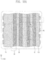
- FIGS. 9A, 10A, 11A, 12A, and 13A are plan views illustrating a method of forming a variable resistance memory device according to some embodiments of the inventive concepts.
- FIGS. 9B, 10B, 11B, 12B, and 13B are cross-sectional views taken along the lines I-I′ of FIGS. 9A to 13A , respectively.
- FIGS. 9C, 10C, 11C, 12C, and 13C are cross-sectional views taken along the lines II-II′ of FIGS. 9A to 13A , respectively.
- FIGS. 14A, 15A, 16A, 17A, 18A, and 19A are plan views illustrating a method of forming a variable resistance memory device according to some embodiments of the inventive concepts.
- FIGS. 14B, 15B 16 B, 17 B, 18 B, and 19 B are cross-sectional views taken along the lines I-I′ of FIGS. 14A to 19A , respectively.
- FIGS. 14C, 15C, 16C, 17C, 18C, and 19C are cross-sectional views taken along the lines II-II′ of FIGS. 14A to 19A , respectively.
- FIGS. 20A and 21A are plan, views illustrating a method of forming a variable resistance memory device according to some embodiments of the inventive concepts.
- FIGS. 20B and 21B are cross-sectional views taken along the lines I-I′ of FIGS. 20A and 21A , respectively.
- FIGS. 20C and 21C are cross-sectional views taken along the lines II-II′ of FIGS. 20A and 21A , respectively.
- variable resistance memory devices and methods of forming the variable resistance memory devices according to the inventive concepts will be described hereinafter with reference to the drawings.
- Like reference numbers refer to like elements throughout.
- an element A overlapping an element B′′ means that there is a vertical line that intersects both the elements A and B that are spaced apart from each other in a vertical direction. It will be also understood that “performed concurrently” (or similar language) refers to performed at approximately (but not necessarily exactly) the same time.
- FIGS. 1A to 8A are plan views illustrating a method of forming a variable resistance memory device according to some embodiments of the inventive concepts.
- FIGS. 1B to 8B are cross-sectional views taken along the lines of FIGS. 1A to 8A , respectively.
- FIGS. 1C to 8C are cross-sectional views taken along the lines II-II′ of FIGS. 1A to 8A , respectively.
- a substrate 100 may be provided.
- the substrate 100 may include a cell region CR and a peripheral region PR.
- Memory cells e.g., MC in FIGS. 8B and 8C
- data e.g., logic data
- transistors for driving the memory cells may be formed on the peripheral region PR of the substrate 100 .
- Each of the memory cells may include a switching element (e.g., SW in FIGS. 8B and 8C ) and a variable resistance structure (e.g., 140 _C in FIGS. 8B and 8C ), which will be described, later herein.
- the cell region CR may be in contact with the peripheral region PR.
- the substrate 100 may include, for example, a single-crystalline semiconductor material.
- the substrate 100 may be a silicon (Si) substrate, a silicon-on-insulator (SOI) substrate, a germanium (Ge) substrate, a germanium-on-insulator (GOI) substrate, or a silicon-germanium (SiGe) substrate.
- Word lines WL and a first interlayer insulating layer 102 may be formed on the substrate 100 .
- a conductive material may be formed on the substrate 100 , and then, a patterning process may be performed on the conductive material to form the word lines WL.
- An insulating layer may be formed on the substrate 100 to cover the word lines WL.
- a planarization process may be performed on the insulating layer to form the first interlayer insulating layer 102 . At this time, top surfaces of the word lines WL may be exposed.
- the first interlayer insulating layer 102 including trenches may be formed on the substrate 100 , and the word lines WL may be formed in the trenches by filling the trenches with a conductive material.
- the word lines WL may extend in a first direction D 1 and may be parallel to each other.
- the first interlayer insulating layer 102 may include, for example, silicon nitride.
- the word lines WL may include at least one of a metal material (e.g., copper (Cu) or aluminum (Al)) or a conductive metal nitride (e.g., titanium nitride (TiN) or tungsten nitride (WN)).
- the first direction D 1 may be referred to as a first horizontal direction that is parallel to an upper surface of the substrate 100 .
- a first insulating layer 104 may be formed on the first interlayer insulating layer 102 .
- the first insulating layer 104 may include first trenches T 1 .
- the first trenches T 1 may extend in a second direction D 2 intersecting the first direction D 1 .
- the second direction D 2 may be referred to as a second horizontal direction that is parallel to an upper surface of the substrate 100 .
- the first trenches T 1 may expose portions of the word lines WL and portions of the first interlayer insulating layer 102 .
- the first insulating layer 104 may include, for example, silicon nitride.
- a conductive layer 106 and a spacer layer 108 may be deposited on the substrate 100 .
- the conductive layer 106 may be formed to conformally cover sidewalls of the first insulating layer 104 exposed by the first trenches T 1 , a top surface of the first insulating layer 104 , top surfaces of the portions of the word lines WL exposed by the first trenches T 1 , and a top surface of the first interlayer insulating layer 102 exposed by the first trenches T 1 .
- the spacer layer 108 may be formed to conformally cover a top surface of the conductive layer 106 .
- the conductive layer 106 may include a conductive material.
- the conductive material may include at least one of W, Ti, Al, Cu, C, CN, TiN, TiAlN, TiSiN, TiCN, WN, CoSiN, WSiN, TaN, TaCN, TaSiN, or TiO.
- the spacer layer 108 may include an insulating material.
- the spacer layer 108 may include silicon oxide.
- the spacer layer 108 may include a conductive material.
- the spacer layer 108 may include poly-silicon.
- the spacer layer 108 may have an etch selectivity with respect to the first interlayer insulating layer 102 and the first insulating layer 104 .
- a portion of the conductive layer 106 and a portion of the spacer layer 108 may be removed.
- the conductive layer 106 and the spacer layer 108 on the boundary region BR may be etched.
- a first mask pattern M 1 may be formed on the substrate 100 .
- the first mask pattern M 1 may cover the cell region CR but may expose the boundary region BR.
- the conductive layer 106 and the spacer layer 108 on the boundary region BR may be removed using the first mask pattern M 1 as a mask (e.g., an etch mask).
- the conductive layer 106 and the spacer layer 108 may be removed to expose a bottom surface of the first trench T 1 on the boundary region BR.
- portions of the top, surfaces of the word lines WL and portions of the top surface of the first interlayer insulating layer 102 may be exposed on the boundary region BR.
- the conductive layer 106 and the spacer layer 108 on the peripheral region PR may also be removed.
- the conductive layer 106 and the spacer layer 108 may remain on the cell region CR but may be removed from the peripheral region PR and the boundary region BR adjacent to the peripheral region PR.
- the conductive layer 106 and the spacer layer 108 on the peripheral region PR may not be removed and may remain on the peripheral region PR.
- the first mask pattern M 1 may cover the cell region CR and the peripheral region PR but may expose the boundary region BR.
- the first mask pattern M 1 may be removed, and then, a second insulating pattern 112 may be formed in the first trenches T 1 .
- a second insulating layer may be formed on the spacer layer 108 to till a remaining region of the first trench T 1 .
- the second insulating layer may also fill the first trenches T 1 on the boundary region BR and the peripheral region PR. In other words, the second insulating layer may be in contact with the bottom surface of the first trench T 1 on the boundary region BR.
- a planarization process may be performed on the second insulating layer, the spacer layer 108 and the conductive layer 106 until the top surface of the first insulating layer 104 is exposed thereby forming an electrode pattern 107 , a spacer pattern 109 and the second insulating pattern 112 , which are sequentially stacked in the first trench T 1 .
- the electrode pattern 107 and the spacer pattern 109 may be formed on the cell region CR but may not be formed on the boundary region BR.
- the second insulating pattern 112 may be formed on both the cell region CR and the boundary region BR.
- the second insulating pattern 112 may be in, contact with the bottom surface of the first trenches T 1 on the boundary region BR.
- the second insulating pattern 112 may be in contact with the top surfaces of the word lines WL exposed by the first trenches T 1 on the boundary region BR.
- the second insulating pattern 112 may insulate a portion of the word line WL on the boundary region BR from a variable resistance structure on the boundary region BR (e.g., 140 _B in FIGS. 8B and 8C ).
- the electrode pattern 107 , the spacer pattern 109 , the first insulating layer 104 , and the second insulating pattern 112 may extend in the second direction D 2 .
- the second insulating pattern 112 may include an insulating material having an etch selectivity with respect to the sparer pattern 109 .
- the second insulating pattern 112 may include silicon nitride.
- second mask patterns M 2 may be formed on the first insulating layer 104 and the second insulating pattern 112 .
- the second mask patterns M 2 may extend in the first direction D 1 and may be parallel to each other.
- the second mask patterns M 2 may expose portions of the electrode pattern 107 , the spacer pattern 109 , the second insulating pattern 112 and the first insulating layer 104 .
- the second mask patterns M 2 may include silicon oxide, silicon nitride, or poly-silicon.
- the electrode pattern 107 , the spacer pattern 109 , the second insulating pattern 112 and the first insulating layer 104 may be patterned using the second, mask patterns M 2 as an etch mask.
- a second trench T 2 may be formed on the top surface of the first interlayer insulating layer 102 between the word lines WL.
- Bottom electrodes BE, spacers 120 , and first insulating patterns 114 may be formed on the word lines WL by the patterning process.
- the electrode pattern 107 may be etched to form the bottom electrodes BE, and the spacer pattern 109 may be etched to form the spacers 120 .
- the first insulating layer 104 may be etched to form the first insulating patterns 114 .
- the second insulating pattern 112 may be formed into a plurality of patterns separated from each other in the second direction D 2 . Sidewalls of the second insulating patterns 112 , which face each other in the second direction D 2 , may be exposed by the second trench T 2 .
- the bottom electrodes BE may be spaced apart from each other in the first direction D 1 and the second direction D 2 . Sidewalls of the bottom electrodes BE, which face each other in, the second direction D 2 , may be exposed by the second trench T 2 .
- Each of the bottom electrodes BE may include a bottom portion BE_B, a first sidewall portion BE_S 1 and a second sidewall portion BE_S 2 , as illustrated in FIG. 7B .
- the bottom portion BE_B may be disposed on the bottom surface of the first trench T 1 and may be electrically connected to the word line WL.
- the first sidewall portion BE_S 1 and the second sidewall portion BE_S 2 may be physically connected to each other through the bottom portion BE_B extending between the spacer 120 and the word line WL.
- first sidewall portion BE_S 1 and the second sidewall portion BE_S 2 may be connected to opposing ends of the bottom portion BE_B, respectively.
- the first sidewall portion BE_S 1 and the second sidewall portion BE_S 2 may extend upwardly from the opposing ends, of the bottom portion BE_B, respectively.
- the first sidewall portion BE_S 1 and the second sidewall portion BE_S 1 may be connected to memory cells (e.g., MC in FIGS. 8B and 8C ), which will be described later, respectively.
- each of the bottom electrodes BE may act as a common electrode of adjacent memory cells due to the first sidewall portion, and the second sidewall portion.
- the first sidewall portion and the second sidewall portion may be physically separated from each other.
- the spacers 120 may be formed between the bottom electrodes BE and the second insulating patterns 112 .
- the spacers 120 may be spaced apart from each other in the first direction D 1 and the second direction D 2 . Sidewalls of the spacers 120 , which face each other in the second direction D 2 , may be exposed by the second trench T 2 .
- the first insulating patterns 114 may be spaced apart from each other in the first direction D 1 and the second direction D 2 .
- the first insulating patterns 114 arranged in the first direction D 1 may be spaced apart from each other with the second insulating pattern 112 , the spacer 120 and the bottom electrode BE interposed therebetween.
- the first insulating patterns 114 arranged in the second direction D 2 may be spaced apart from each other with the second trench T 2 interposed therebetween. Sidewalls of the first insulating patterns 114 , which face each other in the second direction D 2 , may be exposed by the second trench T 2 .
- the second mask patterns M 2 may be removed.
- memory cells MCs and bit lines BL may be formed on the bottom electrodes BE.
- the bit lines BL may extend in the second direction D 2 .
- the memory cells MCs may be formed only on the cell region CR.
- Each of the memory cells MCs may include a switching element SW and a variable resistance structure 140 _C connected in series between the word line WL and the bit BL.
- the switching element SW may not be formed on the boundary region BR
- the second insulating pattern 112 may be disposed between the word line WL and the variable resistance structure 140 _B that is formed on the boundary region BR, as illustrated in FIG. 8B .
- the memory cells MCs may not be formed on the peripheral region PR.
- variable resistance structures 140 include the variable resistance structure 140 _B on the boundary region B and the variable resistance structure 140 _C on the cell region CR.
- variable resistance structure 140 _B that is formed on the boundary region BR may be directly adjacent the variable resistance structure 140 _C that is formed on the cell region CR without any intervening variable resistance structures 140 _B and 140 _C.
- the variable resistance structure 140 _B on the boundary region BR may overlap the word line WL and may be electrically insulated from the word line WL.
- the first insulating pattern 114 and the second insulating pattern 112 may be disposed between the variable resistance structure 140 _B on the boundary region BR and the word line WL and may electrically insulate the variable resistance structure 140 _B from the word line WL.
- a lower surface of the variable resistance structure 140 _B in some embodiments, an entirety of the lower surface of the variable resistance structure 140 _B, may contact the first insulating patterns 114 and the second insulating pattern 112 .
- a portion of the word line WL, that is overlapped by the variable resistance structure 140 _B has an upper surface that faces the variable resistance structure 140 _B and contacts the first insulating patterns 114 and the second insulating pattern 112 .
- variable resistance structure 140 _C on the cell region CR may overlap the word line WL, as illustrated in FIGS. 8B and 8C , and may be configured to be electrically connected to the word line WL through the switching element SW.
- processes of forming the memory cells MCs and the bit lines B 1 will be described in more detail.
- a third insulating pattern 130 may be formed in the second trench T 2 .
- the third insulating pattern 130 may be formed of, for example, the same insulating material as the first insulating patterns 114 and the second insulating patterns 112 .
- the third insulating pattern 130 may include silicon nitride.
- Upper portions of the bottom electrodes BE and upper portions of the spacers 120 may be etched, in some embodiments, sequentially etched. Thus, top surfaces of the bottom electrodes BE and top surfaces of the spacers 120 may be recessed from top surfaces of the first to third insulating patterns 114 , 112 and 130 , and thus inner spaces surrounded by the first to third insulating patterns 114 , 112 and 130 may be formed on the bottom electrodes BE and the spacers 120 . In some embodiments, an etching process for increasing widths of the inner spaces may be performed.
- the switching element SW and an intermediate electrode ME may be sequentially formed in each of the inner spaces.
- the switching elements SW may fill lower regions of the inner spaces.
- the intermediate electrodes ME may be formed on top surfaces of the switching elements SW to fill upper regions, of the inner spaces.
- the switching elements SW may not be formed on the boundary region BR.
- the inner spaces, in which the switching elements SW are formed are formed by sequentially etching the bottom electrodes BE and the spacers 120 , the inner spaces may not be formed on the boundary region BR from which the bottom electrodes BE and the spacers 120 were already removed.
- the switching elements SW may be formed of a compound that includes at least one of Te or Se (i.e., chalcogenide elements) and at least one of Ge, Sb, Bi, Al, Pb, Sn, Ag, As, S, Si, In, Ti, Ga, or P.
- the switching elements SW may further include a thermal stabilization element.
- the thermal stabilization element may include at least one of C, N, or O.
- the switching elements SW may include AsTe, AsSe, GeTe, SnTe, GeSe, SnTe, SnSe,Te, AsTeSe, AsTeGe, AsSeGe, AsTeGeSe, AsSeGeSi, AsSeGeC, AsTeGeSi, AsTeGeS, AsTeGeSiIn, AsTeGeSiP, AsTeGeSiSbS, AsTeGeSiSbP, AsTeGeSeSb, AsTeGeSeSi, AsTeGeSiSeNS, SeTeGeSi, GeSbTeSe, GeBiTeSe, GeAsSbSe, GeAsBiTe, or GeAsBiSe.
- the switching elements SW may have a stronger adhesive strength with an insulating material (e.g., the second insulating pattern 112 ) than with an
- the intermediate electrodes ME may be formed on the switching elements SW, respectively.
- the intermediate electrodes ME may be formed to fill remaining regions of the inner spaces, which are not filled with the switching elements SW.
- the intermediate electrodes ME may include a conductive material such as W, Ti, Al, Cu, C, CN, TiN, TiAlN, TISiN, TiCN, WN, CoSiN, WSiN, TaN, TaCN, TaSiN, and/or TiO.
- a second interlayer insulating layer 150 may be formed on the first to third insulating patterns 114 , 112 and 130 .
- the second interlayer insulating layer 150 may include openings (e.g., holes disposed on the cell region CR. The openings may expose top surfaces of the intermediate electrodes ME, respectively.
- the second interlayer insulating layer 150 may include an insulating material such as silicon nitride.
- variable resistance structures 140 _ 13 and 140 _C and one of top electrodes UE may be sequentially formed in each of the openings.
- the variable resistance structures 140 _ 13 and 140 _C may fill lower regions of the openings, and the top, electrodes UE may be formed on top surfaces of the variable resistance structures 140 _B and 140 _C to fill upper regions of the openings.
- the variable resistance structures 140 _B and 140 _C and the top electrodes UE may be formed on the cell region CR including the boundary region BR but may not be formed on the peripheral region PR.
- the openings in which the variable resistance structures 140 _B and 140 _C and the top electrodes UE are formed may not be formed on the peripheral region PR.
- variable resistance structures 140 _B and 140 _C may include a phase change material.
- the phase change material may be formed of a compound that includes at least one of Te or Se (i.e., chalcogenide elements) and at least one of Ge, Sb, Bi, Pb, Sn, Ag, As, S, Si, In, Ti, Ga, P, O, or C.
- the phase change material may include GeSbTe, GeTeAs, SbTeSe, GeTe, SbTe, SeTeSn, GeTeSe, SbSeBi, GeBiTe, GeTeTi, InSe, GaTeSe, or InSbTe.
- the phase change material may include a perovskite compound or a conductive metal oxide.
- the phase change material may include niobium oxide, titanium oxide, nickel oxide, zirconium oxide, vanadium oxide, (Pr,Ca)MnO 3 (PCMO), strontium-titanium oxide, barium-strontium-titanium oxide, strontium-zirconium oxide, barium-zirconium oxide, or barium-strontium-zirconium oxide.
- PCMO palontium-titanium oxide
- barium-strontium-titanium oxide strontium-zirconium oxide
- barium-zirconium oxide barium-zirconium oxide
- barium-strontium-zirconium oxide barium-strontium-zirconium oxide.
- variable resistance structures 140 _B and 140 _C may have a double-layer structure of a conductive metal oxide layer and a tunnel insulating layer or may have a triple-layer structure of a first conductive metal oxide layer, a tunnel insulating layer and a second conductive metal oxide layer.
- the tunnel insulating layer may include, for example, aluminum oxide, hafnium oxide, and/or silicon oxide.
- the variable resistance structures 140 _B and 140 _C may have a stronger adhesive strength with an insulating material (e.g., the second insulating pattern 112 ) than with a metal material (e.g., the bottom electrode BE).
- the top electrodes UE may include a conductive material such as W, Ti, Al, Cu, C, CN, TiN, TiAlN, TiSiN, TiCN, WN, CoSiN, WSiN, TaN, TaCN, TaSiN, and/or TiO.
- a conductive material such as W, Ti, Al, Cu, C, CN, TiN, TiAlN, TiSiN, TiCN, WN, CoSiN, WSiN, TaN, TaCN, TaSiN, and/or TiO.
- the bit lines BL may be formed on the top electrodes UE.
- the bit lines BL may extend in the second direction D 2 and traverse the word lines WL.
- Each of the hit lines BL may be electrically connected to the top electrodes UE arranged in the second direction D 2 .
- the bit lines BL may include at least one of a metal material (e.g., copper or aluminum) and/or a conductive metal nitride material (e.g., TN or WN).
- a conductive circuit may be formed on the peripheral region PR.
- transistors for driving a semiconductor memory device e.g., the memory cells
- Processes of forming the conductive circuit may include an etching process.
- the memory cells on the cell region CR adjacent to the peripheral region PR may be damaged by the etching process, or portions of the memory cells may be etched by the etching process and the other portions of the memory cells may remain after the etching process.
- some damaged memory cells e.g., damaged variable resistance structures 140 _B
- some damaged memory cells may be electrically connected to the word lines WL.
- a leakage current may flow through the damaged memory cells.
- At least one of the bottom electrode BE and the switching element SW may not be formed on the cell region CR (i.e., the boundary region BR) adjacent to the peripheral region PR.
- the memory cells damaged during the etching process of the peripheral region PR may be electrically insulated from the word lines WL.
- the variable resistance memory device formed according to some embodiments of the inventive concepts may reduce or possibly inhibit a leakage current through damaged memory cells adjacent to a boundary between the cell region CR and the peripheral region PR.
- variable resistance structure 140 _B may be in direct contact with the second insulating pattern 112 on the boundary region BR.
- the variable resistance structure 140 _B may have a stronger adhesive strength with an insulating material (e.g., the second insulating pattern 112 ) than with a conductive material (e.g., the bottom electrode BE).
- an insulating material e.g., the second insulating pattern 112
- a conductive material e.g., the bottom electrode BE
- variable resistance structure 140 _C is disposed on the switching element SW.
- the positions of the switching element SW and the variable resistance structure 140 _C may be reversed.
- the variable resistance structure 140 _C may be formed on the bottom electrode BE
- the intermediate electrode ME may be formed on the variable resistance structure 140 _C
- the switching element SW may be formed between the intermediate electrode ME and the top electrode UE.
- a portion of the conductive layer 106 and a portion of the spacer layer 108 may remain on the boundary region BR.
- FIGS. 9A to 13A are plan views illustrating a method of forming a variable resistance memory device according to some embodiments of the inventive concepts.
- FIGS. 9B to 13B are cross-sectional views taken along the lines I-I′ of FIGS. 9A to 13A , respectively.
- FIGS. 9C to 13C are cross-sectional views taken along the lines II-II′ of FIGS. 9A to 13A , respectively.
- a sacrificial layer 200 may be formed on the resultant structure described with reference to FIGS. 3A to 3C .
- the sacrificial layer 200 may include, for example, a spin-on-hard mask (SOH) layer.
- the sacrificial layer 200 may include a first, sacrificial layer 202 including a carbon-based hard mask material and a second sacrificial layer 204 including a silicon-based hard mask material.
- the first sacrificial layer 202 may fully fill the first trench T 1 .
- the second sacrificial layer 204 may be formed on the first sacrificial layer 202 .
- the sacrificial layer 200 may be patterned.
- the patterned sacrificial layer 200 may cover the cell region CR but may expose the boundary region BR.
- the second sacrificial layer 204 may be patterned, and the first sacrificial layer 202 may be then etched using the patterned second sacrificial layer 204 as an etch mask.
- the first sacrificial layer 202 on the boundary region BR may not be completely removed but may partially remain in the first trench T 1 .
- a remaining portion 202 a of the first sacrificial layer 202 may remain in a lower region of the first trench T 1 on the boundary region BR.
- a height of a top surface of the remaining portion 202 a of the first sacrificial layer 202 may be lower than a height of the top surface of the first insulating layer 104 , as illustrated in FIG. 10B .
- a lower portion of the spacer layer 108 in the first trench T 1 on the boundary region BR may not be exposed by the remaining portion 202 a of the first sacrificial layer 202 .
- the conductive layer 106 and the spacer layer 108 may be etched.
- an etching process may be performed on the spacer layer 108 and the conductive layer 106 by using the sacrificial layer 200 and the remaining portion 202 a of the first sacrificial layer 202 as etch masks.
- a portion of the conductive layer 106 may be removed to form a first portion 162 and a portion of the spacer layer 108 may be removed to form a second portion 164 .
- a sidewall of the first trench T 1 on the boundary region BR may be exposed by the etching process.
- the conductive layer 106 and the spacer layer 108 on the peripheral region PR may also be etched.
- a second insulating pattern 112 may be formed in the first trench T 1 after removing the sacrificial layer 200 and the remaining portion 202 a of the first sacrificial layer 202 .
- a second insulating layer may be formed on the spacer layer 108 to fill a remaining region of the first trench T 1 .
- a planarization process may be performed on the second insulating layer, the spacer layer 108 and the conductive layer 106 until the top surface of the first insulating layer 104 is exposed, thereby forming an electrode pattern 107 , a spacer pattern 109 and the second insulating pattern 112 which are sequentially stacked in the first trench T 1 .
- the second insulating pattern 112 may cover the first portion 162 and the second portion 164 in the first trench T 1 on the boundary region BR.
- the first portion 162 and the second portion 164 may be surrounded by the first insulating layer 104 and the second insulating pattern 112 and may not be exposed.
- second trenches T 2 may be formed to form bottom electrodes BE, spacers 120 , and first insulating patterns 114 , as described with reference to FIGS. 7A to 7C .
- Third insulating patterns 130 may be formed in each of the second trenches T 2 .
- Memory cells and bit lines BL may be formed on the bottom electrodes BE.
- Upper portions of the bottom electrodes BE and upper portions of the spacers 120 may be sequentially etched.
- inner spaces surrounded by the first to third insulating patterns 114 , 112 and 130 may be formed on the bottom electrodes BE and the spacers 120 .
- a switching element SW and an intermediate electrode ME may be sequentially formed in each of the inner spaces.
- variable resistance structure 140 _C and a top electrode UE may be sequentially formed on each of the intermediate electrodes ME on the cell region CR, and a variable resistance structure 140 _B and a top electrode UE may be sequentially formed on the first insulating patterns 114 and, the second insulating pattern 112 .
- one of the variable resistance structures 140 _B and 140 _C and one of the top electrodes UE may be sequentially formed in each of openings (e.g., holes) of the second interlayer insulating layer 150 .
- the variable resistance structures 140 _B and 140 _C and the top electrodes UE may not be formed on the peripheral region PR.
- the variable resistance structure 140 _B that is on boundary region BR and overlaps the first and second portions 162 and 164 may be insulated from the first and second portions 162 and 164 .
- the first and second portions 162 and 164 may be spaced apart from the variable resistance structure 140 _B that overlaps the first and second portions 162 and 164 , and the first insulating patterns 114 and the second insulating pattern 112 may be between the first and second portions 162 and 164 and the variable resistance structure 140 _B as illustrated in FIG. 13B .
- Upper surfaces of the first and second portions 162 and 164 in some embodiments, entireties of the upper surfaces of the first and second portions 162 and 164 , that face the variable resistance structure 140 _B may contact the second insulating pattern 112 .
- a portion of the first sacrificial layer 202 remains in the first trench T 1 after the etching process of the sacrificial layer 200 .
- the first sacrificial layer 202 may be completely removed from the boundary region BR. In this case, the sacrificial layer 200 may act as the first mask pattern M 1 of FIGS. 4A to 4C .
- the process of removing a portion of the conductive layer 106 and a portion of the spacer layer 108 may be performed after the formation of the second trench T 2 .
- FIGS. 14A to 19A are plan views illustrating a method of forming a variable resistance memory device according to some embodiments of the inventive concepts.
- FIGS. 14B to 19B are cross-sectional views taken along the lines I-I′ of FIGS. 14A to 19A , respectively.
- FIGS. 14C to 19C are cross-sectional views taken along the lines II-II′ of FIGS. 14A to 19A , respectively.
- a second insulating layer may be formed on the resultant structure of FIGS. 3A to 3C to fill the first trench T 1 .
- a planarization process may be performed on the second insulating layer, the spacer layer 108 and the conductive layer 106 until, the top surface of the first insulating layer 104 is exposed, thereby forming an electrode pattern 107 , a spacer pattern 109 and a second insulating pattern 112 which are sequentially stacked in the first trench T 1 .
- the electrode pattern 107 , the spacer pattern 109 , the first insulating layer 104 , and, the second insulating pattern 112 may extend in the second direction D 2 .
- the electrode pattern 107 may include a conductive material.
- the spacer pattern 109 may include an insulating material having an etch selectivity with respect to the first interlayer insulating layer 102 and the first insulating layer 104 .
- the spacer pattern 109 may include a conductive material having an etch selectivity with respect to the first interlayer insulating layer 102 and the first insulating layer 104 .
- the second insulating pattern 112 may include an insulating material having an etch selectivity with respect to the spacer pattern 109 .
- second mask patterns M 2 may be formed on the first insulating layer 104 and the second insulating pattern 112 .
- the second mask patterns M 2 may extend in the first direction D 1 and may be parallel to each other.
- the second mask patterns M 2 may expose portions of the electrode pattern 107 , the spacer pattern 109 , the second insulating pattern 112 and the first insulating layer 104 .
- bottom electrodes BE, spacers 120 , and first insulating patterns 114 may be formed on the word lines WL.
- the electrode pattern 107 , the spacer pattern 109 , the second insulating pattern 112 and the first insulating layer 104 may be etched using the second mask patterns M 2 as an etch mask.
- a second trench T 2 may be formed on the top surface of the first interlayer insulating layer 102 between the word lines WL.
- the bottom electrodes BE may be spaced apart from each other in the first direction D 1 and the second direction D 2 .
- the spacers 120 may be formed between the bottom electrodes BE and the second insulating patterns 112 .
- the spacers 120 may be spaced apart from each other in the first direction D 1 and the second direction D 2 .
- the first insulating patterns 114 may be spaced apart from each other in the first direction D 1 and the second direction D 2 .
- the first insulating patterns 114 arranged in the second direction D 2 may be spaced apart from each other with the second trench T 2 interposed therebetween.
- the second mask patterns M 2 may be removed.
- portions of the bottom electrodes BE and portions of the spacers 120 on the boundary region BR may be removed.
- the bottom electrodes BE and the spacers 120 on the boundary region BR may be etched.
- a third insulating pattern 130 may be formed on the substrate 100 .
- the third insulating pattern 130 may cover the cell region CR and may fill the second trench T 2 .
- the bottom electrodes BE and the spacers 120 on the boundary region BR may be etched using the third insulating pattern 130 as an etch mask.
- the third insulating pattern 130 may be formed of, for example, the same insulating material as the first insulating patterns 114 and the second insulating patterns 112 .
- a portion of the bottom electrode BE and, a portion of the spacer 120 may remain in the first trench T 1 on the boundary region BR after the etching process of the bottom electrode BE and the spacer 120 .
- a portion of the bottom electrode BE may be removed to form a third portion 166 and a portion of the spacer 120 may be removed to form a fourth portion 168 .
- a sidewall of the first trench T 1 on the boundary region BR may be exposed by the etching process.
- the bottom electrodes BE and the spacers 120 on the peripheral region PR may also be etched.
- a fourth insulating pattern 116 may be formed on the boundary region BR.
- the fourth insulating pattern 116 may be formed in, in some embodiments may fill a remaining region of the first trench T 1 of the boundary region BR.
- the fourth insulating pattern 116 may be in contact with a top surface of the third portion 166 and a top surface of the fourth portion 168 on the boundary region BR.
- an insulating layer may be formed in the remaining region of the first trench T 1 on the boundary region B.
- the insulating layer may fill the first trench T 1 on the boundary region BR and the peripheral region PR.
- a planarization process may be performed on the insulating layer until top surfaces of the first insulating patterns 114 are exposed, thereby forming the fourth insulating pattern 116 .
- the third insulating pattern 130 may also be planarized.
- the fourth insulating pattern 116 may cover the third portion 166 and the fourth portion 168 in the first trench T 1 on the boundary region BR. In other words, the third portion 166 and the fourth portion 168 may be surrounded by the first to fourth insulating patterns 114 , 112 , 130 and 116 and may not be exposed.
- memory cells and bit lines BL may be formed on the bottom electrodes BE.
- the bit lines DL may extend in the second direction D 2 .
- Each of the memory cells MCs may include a switching element SW and a variable resistance structure 140 _C.
- the variable resistance structure 140 _B on the boundary region BR may be formed on the fourth insulating pattern 116 and may be spaced apart from the third portion 166 and the fourth portion 168 .
- Upper portions of the bottom electrodes BE and upper portions of the spacers 120 that are on the cell region CR may be etched (e.g., sequentially etched) to form inner spaces surrounded by the first to third insulating patterns 114 , 112 and 130 on the bottom electrodes BE and the spacers 120 .
- the switching element SW and an intermediate electrode ME may be sequentially formed in each of the inner spaces.
- the switching elements SW may fill lower regions of the inner spaces
- the intermediate electrodes ME may be formed on top surfaces of the switching elements SW to fill upper regions of the inner spaces.
- the switching elements SW may not be formed on the boundary region BR.
- the intermediate electrodes ME may be formed on the switching elements SW, respectively. In some embodiments, the intermediate electrodes ME may be formed to completely fill remaining regions of the inner spaces, which are not filled with the switching elements SW.
- a second interlayer insulating layer 150 may be formed on the first to third insulating patterns 114 , 112 and 130 .
- the second interlayer insulating layer 150 may have openings (e.g., holes) exposing top surfaces of the intermediate electrodes ME, respectively.
- variable resistance structures 140 _B and 140 _C and one of top electrodes UE may be sequentially formed in each of the openings.
- the variable resistance structures 14 _B and 140 _C may fill lower regions of the openings, and the top electrodes UE may be formed on top surfaces of the variable resistance structures 140 _B and 140 _C to fill upper regions of the openings.
- the bit lines BL may be formed on the top electrodes UE.
- the bit lines BL may extend in the second direction D 2 to intersect the word lines WL.
- Each of the bit lines BL may be electrically connected to the top electrodes UE that are arranged in the second direction D 2 and are spaced apart from each other in the second direction D 2 .
- the memory cells on the peripheral region PR may be removed before the formation of the bit lines BL.
- Transistors for driving a semiconductor memory device e.g., the memory cells
- the peripheral region PR from which the memory cells are removed.
- the process of removing a portion of the conductive layer 106 and a portion of the spacer layer 108 may be performed concurrently with the process of forming the memory cells.
- FIGS. 20A and 21A are plan, views illustrating a method of forming a variable resistance memory device according to some embodiments of the inventive concepts.
- FIGS. 20B and 21B are cross-sectional views taken along the lines I-I′ of FIGS. 20A and 21A , respectively.
- FIGS. 20C and 21C are cross-sectional views taken along the lines II-II′ of FIGS. 20A and 21A , respectively.
- the bottom electrodes BE and the spacers 120 of the resultant structure of FIGS. 16A to 16C may be etched. A portion of each of the bottom electrodes BE and a portion of each of the spacers 120 may remain on the bottom surface of the first trench T 1 after the etching process of the bottom electrodes BE and the spacers 120 . Upper portions of sidewalls of the first trenches T 1 may be exposed by the etching process.
- a fourth insulating pattern 116 may be formed on the boundary region BR.
- the fourth insulating pattern 116 may be formed in, in some embodiments may fill, a remaining region of the first trench T 1 disposed on the boundary region BR.
- a third mask pattern M 3 may be formed to cover the cell region. CR.
- the third mask pattern M 3 may expose the boundary region BR.
- An insulating layer may be formed in the remaining region of the first trench T 1 on the boundary region BR. Due to the third mask pattern M 3 , the insulating layer may not be formed in the first trench T 1 of the cell region CR.
- a planarization process may be performed on the insulating layer and the third mask pattern M 3 until top surfaces of the first insulating patterns 114 are exposed, thereby forming the fourth insulating pattern 116 . Subsequently, a remaining portion of the third mask pattern M 3 may be removed.
- a portion of the bottom electrode BE and a portion of the spacer 120 may remain in the first trench T 1 of the boundary region BR after the etching process of the bottom electrodes BE and the spacers 120 , as illustrated in FIG. 21B .
- the bottom electrodes BE and the spacers 120 on the boundary region BR may be completely removed.
- the memory cells that are damaged during etching processes of forming the transistors on the peripheral region PR may be electrically insulated from the word lines.
- the variable resistance memory device formed according to some embodiments of the inventive concepts may reduce or possibly inhibit a leakage current flowing through the damaged memory cells of the cell region.
- variable resistance memory device may be improved.
Abstract
Description
Claims (15)
Applications Claiming Priority (2)
| Application Number | Priority Date | Filing Date | Title |
|---|---|---|---|
| KR10-2017-0089796 | 2017-07-14 | ||
| KR1020170089796A KR102357987B1 (en) | 2017-07-14 | 2017-07-14 | Variable resistance memory device and method of forming the same |
Publications (2)
| Publication Number | Publication Date |
|---|---|
| US20190019950A1 US20190019950A1 (en) | 2019-01-17 |
| US10714686B2 true US10714686B2 (en) | 2020-07-14 |
Family
ID=65000694
Family Applications (1)
| Application Number | Title | Priority Date | Filing Date |
|---|---|---|---|
| US15/869,892 Active 2038-04-05 US10714686B2 (en) | 2017-07-14 | 2018-01-12 | Variable resistance memory devices and methods of forming the same |
Country Status (3)
| Country | Link |
|---|---|
| US (1) | US10714686B2 (en) |
| KR (1) | KR102357987B1 (en) |
| CN (1) | CN109256406B (en) |
Cited By (1)
| Publication number | Priority date | Publication date | Assignee | Title |
|---|---|---|---|---|
| KR20190008489A (en) * | 2017-07-14 | 2019-01-24 | 삼성전자주식회사 | Variable resistance memory device and method of forming the same |
Citations (8)
| Publication number | Priority date | Publication date | Assignee | Title |
|---|---|---|---|---|
| US20040248339A1 (en) * | 2003-06-06 | 2004-12-09 | Lung Hsiang Lan | High density chalcogenide memory cells |
| KR100819560B1 (en) | 2007-03-26 | 2008-04-08 | 삼성전자주식회사 | Phase change memory device and method of fabricating the same |
| US7554147B2 (en) | 2005-03-15 | 2009-06-30 | Elpida Memory, Inc. | Memory device and manufacturing method thereof |
| KR101124322B1 (en) | 2010-04-12 | 2012-03-27 | 주식회사 하이닉스반도체 | Phase Change Random Access Memory And Method For Fabricating The Same |
| US20120286228A1 (en) * | 2011-05-11 | 2012-11-15 | Min Seok Son | Phase-change random access memory device and method of manufacturing the same |
| JP2014045224A (en) | 2005-03-15 | 2014-03-13 | Ps4 Luxco S A R L | Memory device |
| US20150263071A1 (en) * | 2014-03-11 | 2015-09-17 | SK Hynix Inc. | Electronic device and method for fabricating the same |
| KR20180064084A (en) | 2016-12-05 | 2018-06-14 | 삼성전자주식회사 | Semiconductor device and method for fabricating the same |
Family Cites Families (10)
| Publication number | Priority date | Publication date | Assignee | Title |
|---|---|---|---|---|
| KR100533958B1 (en) * | 2004-01-05 | 2005-12-06 | 삼성전자주식회사 | Phase-change memory device and method of manufacturing the same |
| KR100681266B1 (en) * | 2005-07-25 | 2007-02-09 | 삼성전자주식회사 | Method of manufacturing a variable resistance and method of manufacturing a phase changeable memory device using the same |
| KR101617381B1 (en) * | 2009-12-21 | 2016-05-02 | 삼성전자주식회사 | Resistance variable memory device and method for forming the same |
| KR101920626B1 (en) * | 2011-08-16 | 2018-11-22 | 삼성전자주식회사 | Data storage device and method of fabricating the same |
| KR101917294B1 (en) * | 2012-03-23 | 2018-11-12 | 에스케이하이닉스 주식회사 | Resistance variable memory device and method for fabricating the same |
| KR101994449B1 (en) * | 2012-11-08 | 2019-06-28 | 삼성전자주식회사 | Phase change memory devices and methods for fabricating the same |
| US9349953B2 (en) * | 2013-03-15 | 2016-05-24 | Taiwan Semiconductor Manufacturing Company, Ltd. | Resistance variable memory structure and method of forming the same |
| KR102114202B1 (en) * | 2013-11-25 | 2020-05-26 | 삼성전자주식회사 | Non volatile memory device and method of forming the same |
| KR102316317B1 (en) * | 2015-06-05 | 2021-10-22 | 삼성전자주식회사 | Semiconductor devices and methods of manufacturing the same |
| KR102357987B1 (en) * | 2017-07-14 | 2022-02-04 | 삼성전자주식회사 | Variable resistance memory device and method of forming the same |
-
2017
- 2017-07-14 KR KR1020170089796A patent/KR102357987B1/en active IP Right Grant
-
2018
- 2018-01-12 US US15/869,892 patent/US10714686B2/en active Active
- 2018-07-13 CN CN201810768492.7A patent/CN109256406B/en active Active
Patent Citations (11)
| Publication number | Priority date | Publication date | Assignee | Title |
|---|---|---|---|---|
| US20040248339A1 (en) * | 2003-06-06 | 2004-12-09 | Lung Hsiang Lan | High density chalcogenide memory cells |
| US7554147B2 (en) | 2005-03-15 | 2009-06-30 | Elpida Memory, Inc. | Memory device and manufacturing method thereof |
| JP2014045224A (en) | 2005-03-15 | 2014-03-13 | Ps4 Luxco S A R L | Memory device |
| KR100819560B1 (en) | 2007-03-26 | 2008-04-08 | 삼성전자주식회사 | Phase change memory device and method of fabricating the same |
| US7767568B2 (en) | 2007-03-26 | 2010-08-03 | Samsung Electronics Co., Ltd. | Phase change memory device and method of fabricating the same |
| KR101124322B1 (en) | 2010-04-12 | 2012-03-27 | 주식회사 하이닉스반도체 | Phase Change Random Access Memory And Method For Fabricating The Same |
| US20120286228A1 (en) * | 2011-05-11 | 2012-11-15 | Min Seok Son | Phase-change random access memory device and method of manufacturing the same |
| KR101298189B1 (en) | 2011-05-11 | 2013-08-20 | 에스케이하이닉스 주식회사 | Phase-Change Random Access Memory Device and Fabrication Method Thereof |
| US9136466B2 (en) | 2011-05-11 | 2015-09-15 | Hynix Semiconductor Inc. | Phase-change random access memory device and method of manufacturing the same |
| US20150263071A1 (en) * | 2014-03-11 | 2015-09-17 | SK Hynix Inc. | Electronic device and method for fabricating the same |
| KR20180064084A (en) | 2016-12-05 | 2018-06-14 | 삼성전자주식회사 | Semiconductor device and method for fabricating the same |
Cited By (2)
| Publication number | Priority date | Publication date | Assignee | Title |
|---|---|---|---|---|
| KR20190008489A (en) * | 2017-07-14 | 2019-01-24 | 삼성전자주식회사 | Variable resistance memory device and method of forming the same |
| KR102357987B1 (en) | 2017-07-14 | 2022-02-04 | 삼성전자주식회사 | Variable resistance memory device and method of forming the same |
Also Published As
| Publication number | Publication date |
|---|---|
| KR102357987B1 (en) | 2022-02-04 |
| CN109256406B (en) | 2023-06-20 |
| CN109256406A (en) | 2019-01-22 |
| KR20190008489A (en) | 2019-01-24 |
| US20190019950A1 (en) | 2019-01-17 |
Similar Documents
| Publication | Publication Date | Title |
|---|---|---|
| US11227991B2 (en) | Semiconductor devices | |
| CN106992196B (en) | Variable resistance memory device | |
| KR20170107163A (en) | Semiconductor memory device and method of manufacturing the same | |
| CN109698271B (en) | Variable resistance memory device and method of manufacturing the same | |
| US11245073B2 (en) | Switching element, variable resistance memory device, and method of manufacturing the switching element | |
| US11127900B2 (en) | Variable resistance memory devices, and methods of forming variable resistance memory devices | |
| CN110858623B (en) | Variable resistance memory device and method of manufacturing the same | |
| US20180019281A1 (en) | Variable resistance memory devices and methods of fabricating the same | |
| US20180158872A1 (en) | Variable resistance memory device | |
| US10777745B2 (en) | Switching element, variable resistance memory device, and method of manufacturing the switching element | |
| US20200066985A1 (en) | Variable resistance memory device and method of fabricating the same | |
| US11723221B2 (en) | Three-dimensional semiconductor memory devices | |
| KR20170085409A (en) | Variable resistance memory Device and method of forming the same | |
| US10971548B2 (en) | Variable resistance memory device including symmetrical memory cell arrangements and method of forming the same | |
| US10714686B2 (en) | Variable resistance memory devices and methods of forming the same | |
| US20200083444A1 (en) | Variable resistance memory device and method of manufacturing the same | |
| US11805710B2 (en) | Method of fabricating three-dimensional semiconductor memory device | |
| CN111415956A (en) | Variable resistance memory device and method of manufacturing the same | |
| KR20200093743A (en) | Semiconductor device including data storage pattern and method of manufacturing the same | |
| KR20100076631A (en) | Phase change randomm access memory device and manufacturing method thereof | |
| KR20130087197A (en) | Method for manufacturing phase-change random access memory device |
Legal Events
| Date | Code | Title | Description |
|---|---|---|---|
| AS | Assignment |
Owner name: SAMSUNG ELECTRONICS CO., LTD., KOREA, REPUBLIC OF Free format text: ASSIGNMENT OF ASSIGNORS INTEREST;ASSIGNORS:KIM, SUNGWON;EUN, SUNG-HO;PARK, ILMOK;AND OTHERS;REEL/FRAME:044610/0363 Effective date: 20171212 |
|
| FEPP | Fee payment procedure |
Free format text: ENTITY STATUS SET TO UNDISCOUNTED (ORIGINAL EVENT CODE: BIG.); ENTITY STATUS OF PATENT OWNER: LARGE ENTITY |
|
| STPP | Information on status: patent application and granting procedure in general |
Free format text: DOCKETED NEW CASE - READY FOR EXAMINATION |
|
| STPP | Information on status: patent application and granting procedure in general |
Free format text: NON FINAL ACTION MAILED |
|
| STPP | Information on status: patent application and granting procedure in general |
Free format text: RESPONSE TO NON-FINAL OFFICE ACTION ENTERED AND FORWARDED TO EXAMINER |
|
| STPP | Information on status: patent application and granting procedure in general |
Free format text: FINAL REJECTION MAILED |
|
| STPP | Information on status: patent application and granting procedure in general |
Free format text: NOTICE OF ALLOWANCE MAILED -- APPLICATION RECEIVED IN OFFICE OF PUBLICATIONS |
|
| STPP | Information on status: patent application and granting procedure in general |
Free format text: PUBLICATIONS -- ISSUE FEE PAYMENT VERIFIED |
|
| STCF | Information on status: patent grant |
Free format text: PATENTED CASE |
|
| MAFP | Maintenance fee payment |
Free format text: PAYMENT OF MAINTENANCE FEE, 4TH YEAR, LARGE ENTITY (ORIGINAL EVENT CODE: M1551); ENTITY STATUS OF PATENT OWNER: LARGE ENTITY Year of fee payment: 4 |