US10700190B2 - Semiconductor devices and methods for manufacturing the same - Google Patents
Semiconductor devices and methods for manufacturing the same Download PDFInfo
- Publication number
- US10700190B2 US10700190B2 US15/877,572 US201815877572A US10700190B2 US 10700190 B2 US10700190 B2 US 10700190B2 US 201815877572 A US201815877572 A US 201815877572A US 10700190 B2 US10700190 B2 US 10700190B2
- Authority
- US
- United States
- Prior art keywords
- gallium nitride
- nitride layer
- recess
- semiconductor device
- aluminum gallium
- Prior art date
- Legal status (The legal status is an assumption and is not a legal conclusion. Google has not performed a legal analysis and makes no representation as to the accuracy of the status listed.)
- Active, expires
Links
Images


Classifications
-
- H01L29/7786—
-
- H—ELECTRICITY
- H10—SEMICONDUCTOR DEVICES; ELECTRIC SOLID-STATE DEVICES NOT OTHERWISE PROVIDED FOR
- H10D—INORGANIC ELECTRIC SEMICONDUCTOR DEVICES
- H10D30/00—Field-effect transistors [FET]
- H10D30/40—FETs having zero-dimensional [0D], one-dimensional [1D] or two-dimensional [2D] charge carrier gas channels
- H10D30/47—FETs having zero-dimensional [0D], one-dimensional [1D] or two-dimensional [2D] charge carrier gas channels having 2D charge carrier gas channels, e.g. nanoribbon FETs or high electron mobility transistors [HEMT]
- H10D30/471—High electron mobility transistors [HEMT] or high hole mobility transistors [HHMT]
- H10D30/475—High electron mobility transistors [HEMT] or high hole mobility transistors [HHMT] having wider bandgap layer formed on top of lower bandgap active layer, e.g. undoped barrier HEMTs such as i-AlGaN/GaN HEMTs
-
- H—ELECTRICITY
- H01—ELECTRIC ELEMENTS
- H01L—SEMICONDUCTOR DEVICES NOT COVERED BY CLASS H10
- H01L21/00—Processes or apparatus adapted for the manufacture or treatment of semiconductor or solid state devices or of parts thereof
- H01L21/02—Manufacture or treatment of semiconductor devices or of parts thereof
- H01L21/02104—Forming layers
- H01L21/02365—Forming inorganic semiconducting materials on a substrate
- H01L21/02518—Deposited layers
- H01L21/02521—Materials
- H01L21/02538—Group 13/15 materials
- H01L21/0254—Nitrides
-
- H—ELECTRICITY
- H01—ELECTRIC ELEMENTS
- H01L—SEMICONDUCTOR DEVICES NOT COVERED BY CLASS H10
- H01L21/00—Processes or apparatus adapted for the manufacture or treatment of semiconductor or solid state devices or of parts thereof
- H01L21/02—Manufacture or treatment of semiconductor devices or of parts thereof
- H01L21/04—Manufacture or treatment of semiconductor devices or of parts thereof the devices having potential barriers, e.g. a PN junction, depletion layer or carrier concentration layer
- H01L21/18—Manufacture or treatment of semiconductor devices or of parts thereof the devices having potential barriers, e.g. a PN junction, depletion layer or carrier concentration layer the devices having semiconductor bodies comprising elements of Group IV of the Periodic Table or AIIIBV compounds with or without impurities, e.g. doping materials
- H01L21/30—Treatment of semiconductor bodies using processes or apparatus not provided for in groups H01L21/20 - H01L21/26
- H01L21/302—Treatment of semiconductor bodies using processes or apparatus not provided for in groups H01L21/20 - H01L21/26 to change their surface-physical characteristics or shape, e.g. etching, polishing, cutting
- H01L21/306—Chemical or electrical treatment, e.g. electrolytic etching
- H01L21/308—Chemical or electrical treatment, e.g. electrolytic etching using masks
-
- H01L29/1058—
-
- H01L29/1066—
-
- H01L29/66462—
-
- H—ELECTRICITY
- H10—SEMICONDUCTOR DEVICES; ELECTRIC SOLID-STATE DEVICES NOT OTHERWISE PROVIDED FOR
- H10D—INORGANIC ELECTRIC SEMICONDUCTOR DEVICES
- H10D30/00—Field-effect transistors [FET]
- H10D30/01—Manufacture or treatment
- H10D30/015—Manufacture or treatment of FETs having heterojunction interface channels or heterojunction gate electrodes, e.g. HEMT
-
- H—ELECTRICITY
- H10—SEMICONDUCTOR DEVICES; ELECTRIC SOLID-STATE DEVICES NOT OTHERWISE PROVIDED FOR
- H10D—INORGANIC ELECTRIC SEMICONDUCTOR DEVICES
- H10D62/00—Semiconductor bodies, or regions thereof, of devices having potential barriers
- H10D62/10—Shapes, relative sizes or dispositions of the regions of the semiconductor bodies; Shapes of the semiconductor bodies
- H10D62/17—Semiconductor regions connected to electrodes not carrying current to be rectified, amplified or switched, e.g. channel regions
- H10D62/213—Channel regions of field-effect devices
- H10D62/221—Channel regions of field-effect devices of FETs
- H10D62/328—Channel regions of field-effect devices of FETs having PN junction gates
-
- H—ELECTRICITY
- H10—SEMICONDUCTOR DEVICES; ELECTRIC SOLID-STATE DEVICES NOT OTHERWISE PROVIDED FOR
- H10D—INORGANIC ELECTRIC SEMICONDUCTOR DEVICES
- H10D62/00—Semiconductor bodies, or regions thereof, of devices having potential barriers
- H10D62/10—Shapes, relative sizes or dispositions of the regions of the semiconductor bodies; Shapes of the semiconductor bodies
- H10D62/17—Semiconductor regions connected to electrodes not carrying current to be rectified, amplified or switched, e.g. channel regions
- H10D62/343—Gate regions of field-effect devices having PN junction gates
-
- H10P14/3416—
-
- H10P50/691—
-
- H01L29/2003—
-
- H—ELECTRICITY
- H10—SEMICONDUCTOR DEVICES; ELECTRIC SOLID-STATE DEVICES NOT OTHERWISE PROVIDED FOR
- H10D—INORGANIC ELECTRIC SEMICONDUCTOR DEVICES
- H10D62/00—Semiconductor bodies, or regions thereof, of devices having potential barriers
- H10D62/80—Semiconductor bodies, or regions thereof, of devices having potential barriers characterised by the materials
- H10D62/85—Semiconductor bodies, or regions thereof, of devices having potential barriers characterised by the materials being Group III-V materials, e.g. GaAs
- H10D62/8503—Nitride Group III-V materials, e.g. AlN or GaN
Definitions
- the invention relates to semiconductor devices, and in particular to semiconductor devices having recesses with different depths and methods for manufacturing the same.
- Semiconductor devices are used in a variety of electronic applications, such as high-power devices, personal computers, cell phones, digital cameras, and other electronic devices. These semiconductor devices are typically fabricated by depositing an insulating layer or dielectric layer, a conductive layer material, and a semiconductor layer material on the semiconductor substrate, followed by patterning the various material layers by using a photolithography process. Therefore, the circuit devices and components are formed on the semiconductor substrate.
- HEMTs high-electron mobility transistors
- an upper recess and a lower recess are disposed in an aluminum gallium nitride layer, and a gallium nitride layer is filled in the upper recess and the lower recess.
- the upper recess is adjacent to the lower recess, and the width of the upper recess is greater than the width of the lower recess.
- the bottom surface of the gallium nitride layer is step-shaped.
- the gallium nitride layer has at least two different thicknesses, such that the threshold voltage of the semiconductor device can be easily and precisely controlled without affecting the breakdown voltage of the semiconductor device. Moreover, the threshold voltage can be controlled without adding any additional implantation processes.
- the semiconductor device includes a first gallium nitride layer disposed on a semiconductor substrate, and an aluminum gallium nitride layer disposed on the first gallium nitride layer.
- the semiconductor device also includes an upper recess and a lower recess disposed in the aluminum gallium nitride layer, wherein the upper recess adjoins the lower recess, and the upper recess has a width that is greater than that of the lower recess.
- the semiconductor device further includes a second gallium nitride layer disposed in the first recess and the second recess, and a gate structure disposed on the second gallium nitride layer.
- the semiconductor device includes a source electrode and a drain electrode disposed on the aluminum gallium nitride layer.
- the semiconductor device includes a first gallium nitride layer disposed on a semiconductor substrate, and an aluminum gallium nitride layer disposed on the first gallium nitride layer.
- the semiconductor device also includes a first recess and a second recess disposed in the aluminum gallium nitride layer, wherein the first recess laterally adjoin the second recess, and the second recess has a depth that is greater than that of the first recess.
- the semiconductor device further includes a second gallium nitride layer disposed in the first recess and the second recess, and a gate structure disposed on the second gallium nitride layer.
- the semiconductor device includes a source electrode and a drain electrode disposed on the aluminum gallium nitride layer.
- Some embodiments of the disclosure provide a method for manufacturing a semiconductor device.
- the method includes forming a first gallium nitride layer on a semiconductor substrate, and forming an aluminum gallium nitride layer on the first gallium nitride layer.
- the method also includes forming an upper recess in the aluminum gallium nitride layer, and forming a lower recess in the aluminum gallium nitride layer through the upper recess, wherein the upper recess has a width that is greater than that of the lower recess.
- the method further includes forming a second gallium nitride layer in the lower recess and the upper recess, and forming a gate structure on the second gallium nitride layer.
- the method includes forming a source electrode and a drain electrode on the aluminum gallium nitride layer.
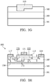
- FIGS. 1A to 1H are cross-sectional views illustrating intermediate stages of a method for manufacturing a semiconductor device of FIG. 1H in accordance with some embodiments.
- FIG. 2 is a cross-sectional view of a semiconductor device of FIG. 2 in accordance with some other embodiments.
- first and second components are formed in direct contact
- additional components may be formed between the first and second components, such that the first and second components may not be in direct contact
- present disclosure may repeat reference numerals and/or letters in the various examples. This repetition is for the purpose of simplicity and clarity and does not in itself dictate a relationship between the various embodiments and/or configurations discussed.
- FIGS. 1A to 1H are cross-sectional views illustrating intermediate stages of a method for manufacturing a semiconductor device 100 of FIG. 1H in accordance with some embodiments.
- a gallium nitride layer 103 (also referred to as a first gallium nitride layer) is formed on a semiconductor substrate 101 .
- the semiconductor substrate 101 may be made of silicon (Si), silicon carbide (SiC), gallium nitride (GaN), silicon dioxide (SiO 2 ), sapphire, or a combination thereof.
- the gallium nitride layer 103 is undoped.
- the gallium nitride layer 103 may be formed by using a metal organic chemical vapor deposition (MOCVD) process, a molecular beam epitaxy (MBE) process, or a combination thereof.
- MOCVD metal organic chemical vapor deposition
- MBE molecular beam epitaxy
- the gallium nitride layer 103 may be a multi-layer structure.
- an aluminum gallium nitride layer 105 is formed on the gallium nitride layer 103 , and a patterned mask 107 is formed on the aluminum gallium nitride layer 105 .
- Some processes used to form the aluminum gallium nitride layer 105 are similar to, or the same as, those used to form the gallium nitride layer 103 , and are not repeated herein.
- the thickness of the aluminum gallium nitride layer 105 is in a range from about 20 nm to about 35 nm, especially about 25 nm.
- the aluminum gallium nitride layer 105 is undoped.
- a mask layer (not shown) is formed on the aluminum gallium nitride layer 105 . Then, the mask layer is patterned by performing a patterning process to form the patterned mask 107 .
- the patterning process includes a photolithography process and an etching process.
- the photolithography process includes photoresist coating (e.g., spin-on coating), soft baking, mask aligning, exposure, post-exposure baking, developing the photoresist, rinsing and drying (e.g., hard baking).
- the etching process includes a dry etching process or a wet etching process. As a result, a portion of the aluminum gallium nitride layer 105 is exposed by the patterned mask 107 .
- an etching process 110 is performed, and an upper recess 109 is formed in the aluminum gallium nitride layer 105 by using the patterned mask 107 as the mask. It is important to note that the upper recess 109 is not penetrating through the aluminum gallium nitride layer 105 . In other words, the gallium nitride layer 103 is not exposed by the upper recess 109 .
- the patterned mask 107 is removed after the upper recess 109 is formed.
- the thickness of the aluminum gallium nitride layer 105 is about 25 nm, and the depth of the upper recess 109 is in a range from about 5 nm to about 10 nm after the etching process 110 . That is, the thickness of the aluminum gallium nitride layer 105 under the upper recess 109 is in a range from about 15 nm to about 20 nm.
- a patterned mask 111 is formed on the aluminum gallium nitride layer 105 , in accordance with some embodiments. Specifically, the patterned mask 111 is extended into the upper recess 109 . A portion of the upper recess 109 is filled by the patterned mask 111 with the other portion of the upper recess 109 remains empty. In some embodiments, one of the sidewalls of the upper recess 109 is aligned with a sidewall of the patterned mask 111 thereon. Some materials and processes used to form the patterned mask 111 are similar to, or the same as, those used to form the patterned mask 107 , and are not repeated herein.
- an etching process 120 is performed, and a lower recess 113 is formed in the aluminum gallium nitride layer 105 through the upper recess 109 by using the patterned mask 111 as the mask.
- the upper recess 109 adjoins the lower recess 113 .
- the upper recess 109 has a sidewall aligned with a sidewall of the lower recess 113 .
- the lower recess 113 has a width W 1
- the upper recess 109 has a width W 2
- the width W 2 is greater than the width W 1 .
- the width W 1 and the width W 2 can be adjusted to meet manufacturing requirements.
- the lower recess 113 is not penetrating through the aluminum gallium nitride layer 105 .
- the gallium nitride layer 103 is not exposed by the lower recess 113 .
- the patterned mask 111 is removed, and a portion of the aluminum gallium nitride layer 105 , which is located under the upper recess 109 and the lower recess 113 , has a step-shaped top surface.
- the combination of the upper recess 109 and the lower recess 113 can be divided into a first recess 123 and a second recess 125 (as shown in FIG. 1F ).
- the first recess 123 laterally adjoins the second recess 125 , and the depth of the second recess 125 is greater than the depth of the first recess 123 .
- a gallium nitride layer 115 (also referred to as a second gallium nitride layer) is filled in the upper recess 109 and the lower recess 113 (i.e., the gallium nitride layer 115 is filled in the first recess 123 and the second recess 125 ).
- the gallium nitride layer 115 protrudes from the aluminum gallium nitride layer 105 .
- the top surface of the gallium nitride layer 115 is higher than the top surface of the aluminum gallium nitride layer 105 .
- the gallium nitride layer 115 may be formed by using a chemical vapor deposition (CVD) process, a metal organic chemical vapor deposition process, a molecular beam epitaxy process, or a combination thereof. In some embodiments, the gallium nitride layer 115 is p-type.
- CVD chemical vapor deposition
- metal organic chemical vapor deposition process a metal organic chemical vapor deposition process
- molecular beam epitaxy process a combination thereof.
- the gallium nitride layer 115 is p-type.
- the bottom surface of the gallium nitride layer 115 is step-shaped, and the gallium nitride layer 103 and the gallium nitride layer 115 are separated by a portion of the aluminum gallium nitride layer 105 .
- the bottommost surface of the gallium nitride layer 115 is higher than the topmost surface of the gallium nitride layer 103 .
- a source electrode 117 and a drain electrode 119 are formed on the aluminum gallium nitride layer 105 , and a gate structure 121 is formed on the gallium nitride layer 115 .
- the source electrode 117 , the drain electrode 119 and the gate structure 121 are made of conductive materials, such as aluminum (Al), copper (Cu), tungsten (W), titanium (Ti), tantalum (Ta), titanium nitride (TiN), or other applicable materials.
- the source electrode 117 , the drain electrode 119 and the gate structure 121 are formed by a deposition process and a patterning process.
- the deposition process may be a chemical vapor deposition process, a physical vapor deposition (PVD) process, an atomic layer deposition (ALD) process, a high density plasma chemical vapor deposition (HDPCVD) process, a metal organic chemical vapor deposition process, a plasma enhanced chemical vapor deposition (PECVD) process, or a combination thereof.
- PVD physical vapor deposition
- ALD atomic layer deposition
- HDPCVD high density plasma chemical vapor deposition
- PECVD plasma enhanced chemical vapor deposition
- the semiconductor device 100 is completed after the source electrode 117 , the drain electrode 119 and the gate structure 123 are formed, and a two-dimensional electron gas (2DEG) channel 130 is generated.
- the two-dimensional electron gas channel 130 may be generated in the gallium nitride layer 103 and may extend along the interface between the gallium nitride layer 103 and the aluminum gallium nitride layer 105 .
- the source electrode 117 is closer to the lower recess 113 than the drain electrode 119 . That is, the source electrode 117 is closer to the second recess 125 than the drain electrode 119 .
- the interface between the first recess 123 and the second recess 125 is covered by the gate structure 121 .
- the bottom surface of the gate structure 121 is higher than the bottom surface of the source electrode 117 and the bottom surface of the drain electrode 119 .
- the aluminum gallium nitride layer 105 has a first thickness T 1 under the first recess 123 , a second thickness T 2 under the second recess 125 , and a third thickness T 3 under the source electrode 117 , and the third thickness T 3 is greater than the first thickness T 1 , the first thickness T 1 is greater than the second thickness T 2 .
- a first ratio of the first thickness T 1 to the third thickness T 3 is in a range from about 0.6 to about 0.8
- a second ratio of the second thickness T 2 to the third thickness T 3 is in a range from about 0.2 to about 0.4.
- the third thickness T 3 is about 25 nm
- the first thickness T 1 is in a range from about 15 nm to about 20 nm
- the second thickness T 2 is in a range from about 5 nm to about 10 nm.
- the portion of the aluminum gallium nitride layer 105 under the gallium nitride layer 115 has two different thicknesses. In other embodiments, the gallium nitride layer 115 may have more than two thicknesses.
- the threshold voltage of the semiconductor device 100 is positively correlated with the second thickness T 2 . Specifically, the threshold voltage of the semiconductor device 100 is increased when the second thickness T 2 is increased. Therefore, the threshold voltage of the semiconductor device 100 can be easily and precisely controlled without affecting the breakdown voltage of the semiconductor device 100 . Moreover, the threshold voltage can be controlled without adding additional implantation processes.
- FIG. 2 is a cross-sectional view of a semiconductor device 200 of FIG. 2 in accordance with some other embodiments.
- the difference between the semiconductor device 200 and the semiconductor device 100 is the positions of the recesses.
- the semiconductor device 200 includes an aluminum gallium nitride layer 205 . Some materials and processes used to form the aluminum gallium nitride layer 205 are similar to, or the same as, those used to form the aluminum gallium nitride layer 105 of the semiconductor device 100 , and are not repeated herein.
- the semiconductor device 200 includes a first recess 223 and a second recess 225 . Some processes used to form the first recess 223 and the second recess 225 are similar to, or the same as, those used to form the first recess 123 and the second recess 125 (i.e. the upper recess 109 and the lower recess 113 ) of the semiconductor device 100 , and are not repeated herein. However, the first recess 223 of the semiconductor device 200 is closer to the source electrode 117 than the second recess 225 , which is different from the semiconductor device 100 .
- the first thickness T 1 of the aluminum gallium nitride layer 205 in the semiconductor device 200 is closer to the source electrode 117 than the first thickness T 1 of the aluminum gallium nitride layer 105 in the semiconductor device 100 .
- an upper recess and a lower recess are disposed in an aluminum gallium nitride layer, and a gallium nitride layer is filled in the upper recess and the lower recess.
- the upper recess adjoins the lower recess, and the width of the upper recess is greater than the width of the lower recess.
- the bottom surface of the gallium nitride layer is step-shaped. That is, the gallium nitride layer has at least two different thicknesses, such that the threshold voltage of the semiconductor device can be easily and precisely controlled without affecting the breakdown voltage of the semiconductor device. Moreover, the threshold voltage can be controlled without adding additional implantation processes.
Landscapes
- Engineering & Computer Science (AREA)
- Physics & Mathematics (AREA)
- Condensed Matter Physics & Semiconductors (AREA)
- General Physics & Mathematics (AREA)
- Manufacturing & Machinery (AREA)
- Computer Hardware Design (AREA)
- Microelectronics & Electronic Packaging (AREA)
- Power Engineering (AREA)
- Junction Field-Effect Transistors (AREA)
- Electrodes Of Semiconductors (AREA)
Abstract
Description
Claims (14)
Priority Applications (1)
| Application Number | Priority Date | Filing Date | Title |
|---|---|---|---|
| US15/877,572 US10700190B2 (en) | 2018-01-23 | 2018-01-23 | Semiconductor devices and methods for manufacturing the same |
Applications Claiming Priority (1)
| Application Number | Priority Date | Filing Date | Title |
|---|---|---|---|
| US15/877,572 US10700190B2 (en) | 2018-01-23 | 2018-01-23 | Semiconductor devices and methods for manufacturing the same |
Publications (2)
| Publication Number | Publication Date |
|---|---|
| US20190229209A1 US20190229209A1 (en) | 2019-07-25 |
| US10700190B2 true US10700190B2 (en) | 2020-06-30 |
Family
ID=67298292
Family Applications (1)
| Application Number | Title | Priority Date | Filing Date |
|---|---|---|---|
| US15/877,572 Active 2038-02-19 US10700190B2 (en) | 2018-01-23 | 2018-01-23 | Semiconductor devices and methods for manufacturing the same |
Country Status (1)
| Country | Link |
|---|---|
| US (1) | US10700190B2 (en) |
Families Citing this family (4)
| Publication number | Priority date | Publication date | Assignee | Title |
|---|---|---|---|---|
| CN112310212B (en) * | 2020-07-14 | 2025-06-03 | 中山市华南理工大学现代产业技术研究院 | A high linearity GaN-based millimeter wave device and its preparation method |
| WO2022087869A1 (en) * | 2020-10-28 | 2022-05-05 | Innoscience (Suzhou) Technology Co., Ltd. | Semiconductor device and fabrication method thereof |
| JPWO2024171753A1 (en) * | 2023-02-13 | 2024-08-22 | ||
| KR102836581B1 (en) * | 2023-09-27 | 2025-07-22 | 주식회사 에이프로세미콘 | Semiconductor device |
Citations (9)
| Publication number | Priority date | Publication date | Assignee | Title |
|---|---|---|---|---|
| US20110057257A1 (en) * | 2009-09-08 | 2011-03-10 | Samsung Electro-Mechanics Co., Ltd. | Semiconductor device and method for manufacturing the same |
| US20110127540A1 (en) * | 2009-11-30 | 2011-06-02 | Sumitomo Electric Industries, Ltd. | Semiconductor device |
| TW201301400A (en) | 2011-06-29 | 2013-01-01 | 財團法人工業技術研究院 | Transistor element and method of manufacturing same |
| US20140091316A1 (en) * | 2012-09-28 | 2014-04-03 | Fujitsu Limited | Semiconductor device and manufacturing method of semiconductor device |
| US20140097468A1 (en) * | 2011-07-12 | 2014-04-10 | Panasonic Corporation | Nitride semiconductor device and method for manufacturing same |
| TW201427000A (en) | 2012-12-19 | 2014-07-01 | Ind Tech Res Inst | Enhancement mode gallium nitride based transistor device |
| TW201503364A (en) | 2013-07-11 | 2015-01-16 | Univ Asia | High electron mobility transistor and manufacturing method thereof |
| TW201541636A (en) | 2014-04-30 | 2015-11-01 | 台灣積體電路製造股份有限公司 | High electron mobility transistor and method of manufacturing same |
| US20160043209A1 (en) * | 2013-04-11 | 2016-02-11 | Denso Corporation | Semiconductor device provided with hemt |
-
2018
- 2018-01-23 US US15/877,572 patent/US10700190B2/en active Active
Patent Citations (9)
| Publication number | Priority date | Publication date | Assignee | Title |
|---|---|---|---|---|
| US20110057257A1 (en) * | 2009-09-08 | 2011-03-10 | Samsung Electro-Mechanics Co., Ltd. | Semiconductor device and method for manufacturing the same |
| US20110127540A1 (en) * | 2009-11-30 | 2011-06-02 | Sumitomo Electric Industries, Ltd. | Semiconductor device |
| TW201301400A (en) | 2011-06-29 | 2013-01-01 | 財團法人工業技術研究院 | Transistor element and method of manufacturing same |
| US20140097468A1 (en) * | 2011-07-12 | 2014-04-10 | Panasonic Corporation | Nitride semiconductor device and method for manufacturing same |
| US20140091316A1 (en) * | 2012-09-28 | 2014-04-03 | Fujitsu Limited | Semiconductor device and manufacturing method of semiconductor device |
| TW201427000A (en) | 2012-12-19 | 2014-07-01 | Ind Tech Res Inst | Enhancement mode gallium nitride based transistor device |
| US20160043209A1 (en) * | 2013-04-11 | 2016-02-11 | Denso Corporation | Semiconductor device provided with hemt |
| TW201503364A (en) | 2013-07-11 | 2015-01-16 | Univ Asia | High electron mobility transistor and manufacturing method thereof |
| TW201541636A (en) | 2014-04-30 | 2015-11-01 | 台灣積體電路製造股份有限公司 | High electron mobility transistor and method of manufacturing same |
Also Published As
| Publication number | Publication date |
|---|---|
| US20190229209A1 (en) | 2019-07-25 |
Similar Documents
| Publication | Publication Date | Title |
|---|---|---|
| US12027603B2 (en) | Semiconductor device | |
| CN105938799B (en) | Method for manufacturing semiconductor device and semiconductor device | |
| US11398546B2 (en) | Semiconductor devices and methods for fabricating the same | |
| US10535653B2 (en) | Semiconductor structure | |
| CN110071173A (en) | Semiconductor device and its manufacturing method | |
| US10700190B2 (en) | Semiconductor devices and methods for manufacturing the same | |
| TWI533452B (en) | Compound semiconductor device and method of manufacturing same | |
| US11855128B2 (en) | Metal insulator metal (MIM) structure and manufacturing method thereof | |
| KR20070029830A (en) | Integrated circuits and their formation methods | |
| TWI661555B (en) | Enhancement mode hemt device | |
| TWI674631B (en) | Semiconductor devices and methods for forming the same | |
| CN109980000A (en) | Enhancement type high electron mobility transistor element and forming method thereof | |
| US10903350B2 (en) | Semiconductor devices and methods for forming the same | |
| CN110875383B (en) | Semiconductor device and method for manufacturing the same | |
| TWI678731B (en) | Semiconductor devices and methods for manufacturing the same | |
| CN110890414B (en) | Semiconductor device and manufacturing method thereof |
Legal Events
| Date | Code | Title | Description |
|---|---|---|---|
| FEPP | Fee payment procedure |
Free format text: ENTITY STATUS SET TO UNDISCOUNTED (ORIGINAL EVENT CODE: BIG.); ENTITY STATUS OF PATENT OWNER: LARGE ENTITY |
|
| AS | Assignment |
Owner name: VANGUARD INTERNATIONAL SEMICONDUCTOR CORPORATION, Free format text: ASSIGNMENT OF ASSIGNORS INTEREST;ASSIGNORS:LEE, CHIA-HAO;KUMAR, MANOJ;HUNG, CHANG-XIANG;AND OTHERS;SIGNING DATES FROM 20180104 TO 20180109;REEL/FRAME:044715/0755 Owner name: VANGUARD INTERNATIONAL SEMICONDUCTOR CORPORATION, TAIWAN Free format text: ASSIGNMENT OF ASSIGNORS INTEREST;ASSIGNORS:LEE, CHIA-HAO;KUMAR, MANOJ;HUNG, CHANG-XIANG;AND OTHERS;SIGNING DATES FROM 20180104 TO 20180109;REEL/FRAME:044715/0755 |
|
| STPP | Information on status: patent application and granting procedure in general |
Free format text: DOCKETED NEW CASE - READY FOR EXAMINATION |
|
| STPP | Information on status: patent application and granting procedure in general |
Free format text: NON FINAL ACTION MAILED |
|
| STPP | Information on status: patent application and granting procedure in general |
Free format text: RESPONSE TO NON-FINAL OFFICE ACTION ENTERED AND FORWARDED TO EXAMINER |
|
| STPP | Information on status: patent application and granting procedure in general |
Free format text: NOTICE OF ALLOWANCE MAILED -- APPLICATION RECEIVED IN OFFICE OF PUBLICATIONS |
|
| STPP | Information on status: patent application and granting procedure in general |
Free format text: PUBLICATIONS -- ISSUE FEE PAYMENT RECEIVED |
|
| STCF | Information on status: patent grant |
Free format text: PATENTED CASE |
|
| MAFP | Maintenance fee payment |
Free format text: PAYMENT OF MAINTENANCE FEE, 4TH YEAR, LARGE ENTITY (ORIGINAL EVENT CODE: M1551); ENTITY STATUS OF PATENT OWNER: LARGE ENTITY Year of fee payment: 4 |