US10700024B2 - Fan-out semiconductor package - Google Patents
Fan-out semiconductor package Download PDFInfo
- Publication number
- US10700024B2 US10700024B2 US15/958,573 US201815958573A US10700024B2 US 10700024 B2 US10700024 B2 US 10700024B2 US 201815958573 A US201815958573 A US 201815958573A US 10700024 B2 US10700024 B2 US 10700024B2
- Authority
- US
- United States
- Prior art keywords
- fan
- semiconductor package
- semiconductor chip
- disposed
- out semiconductor
- Prior art date
- Legal status (The legal status is an assumption and is not a legal conclusion. Google has not performed a legal analysis and makes no representation as to the accuracy of the status listed.)
- Active
Links
Images


Classifications
-
- H—ELECTRICITY
- H01—ELECTRIC ELEMENTS
- H01Q—ANTENNAS, i.e. RADIO AERIALS
- H01Q1/00—Details of, or arrangements associated with, antennas
- H01Q1/12—Supports; Mounting means
- H01Q1/22—Supports; Mounting means by structural association with other equipment or articles
- H01Q1/2283—Supports; Mounting means by structural association with other equipment or articles mounted in or on the surface of a semiconductor substrate as a chip-type antenna or integrated with other components into an IC package
-
- H—ELECTRICITY
- H01—ELECTRIC ELEMENTS
- H01L—SEMICONDUCTOR DEVICES NOT COVERED BY CLASS H10
- H01L23/00—Details of semiconductor or other solid state devices
- H01L23/58—Structural electrical arrangements for semiconductor devices not otherwise provided for, e.g. in combination with batteries
- H01L23/64—Impedance arrangements
- H01L23/66—High-frequency adaptations
-
- H—ELECTRICITY
- H01—ELECTRIC ELEMENTS
- H01L—SEMICONDUCTOR DEVICES NOT COVERED BY CLASS H10
- H01L21/00—Processes or apparatus adapted for the manufacture or treatment of semiconductor or solid state devices or of parts thereof
- H01L21/02—Manufacture or treatment of semiconductor devices or of parts thereof
- H01L21/04—Manufacture or treatment of semiconductor devices or of parts thereof the devices having potential barriers, e.g. a PN junction, depletion layer or carrier concentration layer
- H01L21/50—Assembly of semiconductor devices using processes or apparatus not provided for in a single one of the groups H01L21/18 - H01L21/326 or H10D48/04 - H10D48/07 e.g. sealing of a cap to a base of a container
- H01L21/56—Encapsulations, e.g. encapsulation layers, coatings
- H01L21/568—Temporary substrate used as encapsulation process aid
-
- H—ELECTRICITY
- H01—ELECTRIC ELEMENTS
- H01L—SEMICONDUCTOR DEVICES NOT COVERED BY CLASS H10
- H01L23/00—Details of semiconductor or other solid state devices
- H01L23/28—Encapsulations, e.g. encapsulating layers, coatings, e.g. for protection
- H01L23/31—Encapsulations, e.g. encapsulating layers, coatings, e.g. for protection characterised by the arrangement or shape
- H01L23/3107—Encapsulations, e.g. encapsulating layers, coatings, e.g. for protection characterised by the arrangement or shape the device being completely enclosed
- H01L23/3121—Encapsulations, e.g. encapsulating layers, coatings, e.g. for protection characterised by the arrangement or shape the device being completely enclosed a substrate forming part of the encapsulation
- H01L23/3128—Encapsulations, e.g. encapsulating layers, coatings, e.g. for protection characterised by the arrangement or shape the device being completely enclosed a substrate forming part of the encapsulation the substrate having spherical bumps for external connection
-
- H—ELECTRICITY
- H01—ELECTRIC ELEMENTS
- H01L—SEMICONDUCTOR DEVICES NOT COVERED BY CLASS H10
- H01L24/00—Arrangements for connecting or disconnecting semiconductor or solid-state bodies; Methods or apparatus related thereto
- H01L24/01—Means for bonding being attached to, or being formed on, the surface to be connected, e.g. chip-to-package, die-attach, "first-level" interconnects; Manufacturing methods related thereto
- H01L24/02—Bonding areas ; Manufacturing methods related thereto
- H01L24/07—Structure, shape, material or disposition of the bonding areas after the connecting process
- H01L24/09—Structure, shape, material or disposition of the bonding areas after the connecting process of a plurality of bonding areas
-
- H—ELECTRICITY
- H01—ELECTRIC ELEMENTS
- H01L—SEMICONDUCTOR DEVICES NOT COVERED BY CLASS H10
- H01L24/00—Arrangements for connecting or disconnecting semiconductor or solid-state bodies; Methods or apparatus related thereto
- H01L24/01—Means for bonding being attached to, or being formed on, the surface to be connected, e.g. chip-to-package, die-attach, "first-level" interconnects; Manufacturing methods related thereto
- H01L24/10—Bump connectors ; Manufacturing methods related thereto
- H01L24/12—Structure, shape, material or disposition of the bump connectors prior to the connecting process
- H01L24/14—Structure, shape, material or disposition of the bump connectors prior to the connecting process of a plurality of bump connectors
-
- H—ELECTRICITY
- H01—ELECTRIC ELEMENTS
- H01L—SEMICONDUCTOR DEVICES NOT COVERED BY CLASS H10
- H01L24/00—Arrangements for connecting or disconnecting semiconductor or solid-state bodies; Methods or apparatus related thereto
- H01L24/01—Means for bonding being attached to, or being formed on, the surface to be connected, e.g. chip-to-package, die-attach, "first-level" interconnects; Manufacturing methods related thereto
- H01L24/10—Bump connectors ; Manufacturing methods related thereto
- H01L24/15—Structure, shape, material or disposition of the bump connectors after the connecting process
- H01L24/17—Structure, shape, material or disposition of the bump connectors after the connecting process of a plurality of bump connectors
-
- H—ELECTRICITY
- H01—ELECTRIC ELEMENTS
- H01L—SEMICONDUCTOR DEVICES NOT COVERED BY CLASS H10
- H01L24/00—Arrangements for connecting or disconnecting semiconductor or solid-state bodies; Methods or apparatus related thereto
- H01L24/01—Means for bonding being attached to, or being formed on, the surface to be connected, e.g. chip-to-package, die-attach, "first-level" interconnects; Manufacturing methods related thereto
- H01L24/18—High density interconnect [HDI] connectors; Manufacturing methods related thereto
- H01L24/19—Manufacturing methods of high density interconnect preforms
-
- H—ELECTRICITY
- H01—ELECTRIC ELEMENTS
- H01L—SEMICONDUCTOR DEVICES NOT COVERED BY CLASS H10
- H01L24/00—Arrangements for connecting or disconnecting semiconductor or solid-state bodies; Methods or apparatus related thereto
- H01L24/01—Means for bonding being attached to, or being formed on, the surface to be connected, e.g. chip-to-package, die-attach, "first-level" interconnects; Manufacturing methods related thereto
- H01L24/18—High density interconnect [HDI] connectors; Manufacturing methods related thereto
- H01L24/20—Structure, shape, material or disposition of high density interconnect preforms
-
- H—ELECTRICITY
- H01—ELECTRIC ELEMENTS
- H01Q—ANTENNAS, i.e. RADIO AERIALS
- H01Q1/00—Details of, or arrangements associated with, antennas
- H01Q1/36—Structural form of radiating elements, e.g. cone, spiral, umbrella; Particular materials used therewith
- H01Q1/38—Structural form of radiating elements, e.g. cone, spiral, umbrella; Particular materials used therewith formed by a conductive layer on an insulating support
-
- H—ELECTRICITY
- H01—ELECTRIC ELEMENTS
- H01Q—ANTENNAS, i.e. RADIO AERIALS
- H01Q1/00—Details of, or arrangements associated with, antennas
- H01Q1/48—Earthing means; Earth screens; Counterpoises
-
- H—ELECTRICITY
- H01—ELECTRIC ELEMENTS
- H01Q—ANTENNAS, i.e. RADIO AERIALS
- H01Q21/00—Antenna arrays or systems
- H01Q21/06—Arrays of individually energised antenna units similarly polarised and spaced apart
- H01Q21/061—Two dimensional planar arrays
- H01Q21/065—Patch antenna array
-
- H—ELECTRICITY
- H01—ELECTRIC ELEMENTS
- H01Q—ANTENNAS, i.e. RADIO AERIALS
- H01Q9/00—Electrically-short antennas having dimensions not more than twice the operating wavelength and consisting of conductive active radiating elements
- H01Q9/04—Resonant antennas
- H01Q9/0407—Substantially flat resonant element parallel to ground plane, e.g. patch antenna
-
- H10W44/20—
-
- H10W70/09—
-
- H10W70/60—
-
- H10W72/20—
-
- H10W72/90—
-
- H10W74/019—
-
- H10W74/111—
-
- H10W74/117—
-
- H—ELECTRICITY
- H01—ELECTRIC ELEMENTS
- H01L—SEMICONDUCTOR DEVICES NOT COVERED BY CLASS H10
- H01L2223/00—Details relating to semiconductor or other solid state devices covered by the group H01L23/00
- H01L2223/58—Structural electrical arrangements for semiconductor devices not otherwise provided for
- H01L2223/64—Impedance arrangements
- H01L2223/66—High-frequency adaptations
- H01L2223/6661—High-frequency adaptations for passive devices
- H01L2223/6677—High-frequency adaptations for passive devices for antenna, e.g. antenna included within housing of semiconductor device
-
- H—ELECTRICITY
- H01—ELECTRIC ELEMENTS
- H01L—SEMICONDUCTOR DEVICES NOT COVERED BY CLASS H10
- H01L2224/00—Indexing scheme for arrangements for connecting or disconnecting semiconductor or solid-state bodies and methods related thereto as covered by H01L24/00
- H01L2224/01—Means for bonding being attached to, or being formed on, the surface to be connected, e.g. chip-to-package, die-attach, "first-level" interconnects; Manufacturing methods related thereto
- H01L2224/02—Bonding areas; Manufacturing methods related thereto
- H01L2224/023—Redistribution layers [RDL] for bonding areas
- H01L2224/0237—Disposition of the redistribution layers
- H01L2224/02379—Fan-out arrangement
-
- H—ELECTRICITY
- H01—ELECTRIC ELEMENTS
- H01L—SEMICONDUCTOR DEVICES NOT COVERED BY CLASS H10
- H01L2224/00—Indexing scheme for arrangements for connecting or disconnecting semiconductor or solid-state bodies and methods related thereto as covered by H01L24/00
- H01L2224/01—Means for bonding being attached to, or being formed on, the surface to be connected, e.g. chip-to-package, die-attach, "first-level" interconnects; Manufacturing methods related thereto
- H01L2224/02—Bonding areas; Manufacturing methods related thereto
- H01L2224/04—Structure, shape, material or disposition of the bonding areas prior to the connecting process
- H01L2224/0401—Bonding areas specifically adapted for bump connectors, e.g. under bump metallisation [UBM]
-
- H—ELECTRICITY
- H01—ELECTRIC ELEMENTS
- H01L—SEMICONDUCTOR DEVICES NOT COVERED BY CLASS H10
- H01L2224/00—Indexing scheme for arrangements for connecting or disconnecting semiconductor or solid-state bodies and methods related thereto as covered by H01L24/00
- H01L2224/01—Means for bonding being attached to, or being formed on, the surface to be connected, e.g. chip-to-package, die-attach, "first-level" interconnects; Manufacturing methods related thereto
- H01L2224/10—Bump connectors; Manufacturing methods related thereto
- H01L2224/12—Structure, shape, material or disposition of the bump connectors prior to the connecting process
- H01L2224/13—Structure, shape, material or disposition of the bump connectors prior to the connecting process of an individual bump connector
- H01L2224/13001—Core members of the bump connector
- H01L2224/13099—Material
- H01L2224/131—Material with a principal constituent of the material being a metal or a metalloid, e.g. boron [B], silicon [Si], germanium [Ge], arsenic [As], antimony [Sb], tellurium [Te] and polonium [Po], and alloys thereof
- H01L2224/13101—Material with a principal constituent of the material being a metal or a metalloid, e.g. boron [B], silicon [Si], germanium [Ge], arsenic [As], antimony [Sb], tellurium [Te] and polonium [Po], and alloys thereof the principal constituent melting at a temperature of less than 400°C
-
- H—ELECTRICITY
- H01—ELECTRIC ELEMENTS
- H01L—SEMICONDUCTOR DEVICES NOT COVERED BY CLASS H10
- H01L2224/00—Indexing scheme for arrangements for connecting or disconnecting semiconductor or solid-state bodies and methods related thereto as covered by H01L24/00
- H01L2224/01—Means for bonding being attached to, or being formed on, the surface to be connected, e.g. chip-to-package, die-attach, "first-level" interconnects; Manufacturing methods related thereto
- H01L2224/10—Bump connectors; Manufacturing methods related thereto
- H01L2224/15—Structure, shape, material or disposition of the bump connectors after the connecting process
- H01L2224/16—Structure, shape, material or disposition of the bump connectors after the connecting process of an individual bump connector
- H01L2224/161—Disposition
- H01L2224/16151—Disposition the bump connector connecting between a semiconductor or solid-state body and an item not being a semiconductor or solid-state body, e.g. chip-to-substrate, chip-to-passive
- H01L2224/16221—Disposition the bump connector connecting between a semiconductor or solid-state body and an item not being a semiconductor or solid-state body, e.g. chip-to-substrate, chip-to-passive the body and the item being stacked
- H01L2224/16225—Disposition the bump connector connecting between a semiconductor or solid-state body and an item not being a semiconductor or solid-state body, e.g. chip-to-substrate, chip-to-passive the body and the item being stacked the item being non-metallic, e.g. insulating substrate with or without metallisation
-
- H—ELECTRICITY
- H01—ELECTRIC ELEMENTS
- H01L—SEMICONDUCTOR DEVICES NOT COVERED BY CLASS H10
- H01L2224/00—Indexing scheme for arrangements for connecting or disconnecting semiconductor or solid-state bodies and methods related thereto as covered by H01L24/00
- H01L2224/01—Means for bonding being attached to, or being formed on, the surface to be connected, e.g. chip-to-package, die-attach, "first-level" interconnects; Manufacturing methods related thereto
- H01L2224/26—Layer connectors, e.g. plate connectors, solder or adhesive layers; Manufacturing methods related thereto
- H01L2224/31—Structure, shape, material or disposition of the layer connectors after the connecting process
- H01L2224/32—Structure, shape, material or disposition of the layer connectors after the connecting process of an individual layer connector
- H01L2224/321—Disposition
- H01L2224/32151—Disposition the layer connector connecting between a semiconductor or solid-state body and an item not being a semiconductor or solid-state body, e.g. chip-to-substrate, chip-to-passive
- H01L2224/32221—Disposition the layer connector connecting between a semiconductor or solid-state body and an item not being a semiconductor or solid-state body, e.g. chip-to-substrate, chip-to-passive the body and the item being stacked
- H01L2224/32225—Disposition the layer connector connecting between a semiconductor or solid-state body and an item not being a semiconductor or solid-state body, e.g. chip-to-substrate, chip-to-passive the body and the item being stacked the item being non-metallic, e.g. insulating substrate with or without metallisation
-
- H—ELECTRICITY
- H01—ELECTRIC ELEMENTS
- H01L—SEMICONDUCTOR DEVICES NOT COVERED BY CLASS H10
- H01L2224/00—Indexing scheme for arrangements for connecting or disconnecting semiconductor or solid-state bodies and methods related thereto as covered by H01L24/00
- H01L2224/73—Means for bonding being of different types provided for in two or more of groups H01L2224/10, H01L2224/18, H01L2224/26, H01L2224/34, H01L2224/42, H01L2224/50, H01L2224/63, H01L2224/71
- H01L2224/732—Location after the connecting process
- H01L2224/73201—Location after the connecting process on the same surface
- H01L2224/73203—Bump and layer connectors
- H01L2224/73204—Bump and layer connectors the bump connector being embedded into the layer connector
-
- H—ELECTRICITY
- H01—ELECTRIC ELEMENTS
- H01L—SEMICONDUCTOR DEVICES NOT COVERED BY CLASS H10
- H01L2924/00—Indexing scheme for arrangements or methods for connecting or disconnecting semiconductor or solid-state bodies as covered by H01L24/00
-
- H—ELECTRICITY
- H01—ELECTRIC ELEMENTS
- H01L—SEMICONDUCTOR DEVICES NOT COVERED BY CLASS H10
- H01L2924/00—Indexing scheme for arrangements or methods for connecting or disconnecting semiconductor or solid-state bodies as covered by H01L24/00
- H01L2924/0001—Technical content checked by a classifier
- H01L2924/00012—Relevant to the scope of the group, the symbol of which is combined with the symbol of this group
-
- H—ELECTRICITY
- H01—ELECTRIC ELEMENTS
- H01L—SEMICONDUCTOR DEVICES NOT COVERED BY CLASS H10
- H01L2924/00—Indexing scheme for arrangements or methods for connecting or disconnecting semiconductor or solid-state bodies as covered by H01L24/00
- H01L2924/0001—Technical content checked by a classifier
- H01L2924/00014—Technical content checked by a classifier the subject-matter covered by the group, the symbol of which is combined with the symbol of this group, being disclosed without further technical details
-
- H—ELECTRICITY
- H01—ELECTRIC ELEMENTS
- H01L—SEMICONDUCTOR DEVICES NOT COVERED BY CLASS H10
- H01L2924/00—Indexing scheme for arrangements or methods for connecting or disconnecting semiconductor or solid-state bodies as covered by H01L24/00
- H01L2924/013—Alloys
- H01L2924/014—Solder alloys
-
- H—ELECTRICITY
- H01—ELECTRIC ELEMENTS
- H01L—SEMICONDUCTOR DEVICES NOT COVERED BY CLASS H10
- H01L2924/00—Indexing scheme for arrangements or methods for connecting or disconnecting semiconductor or solid-state bodies as covered by H01L24/00
- H01L2924/10—Details of semiconductor or other solid state devices to be connected
- H01L2924/11—Device type
- H01L2924/14—Integrated circuits
- H01L2924/143—Digital devices
- H01L2924/1431—Logic devices
-
- H—ELECTRICITY
- H01—ELECTRIC ELEMENTS
- H01L—SEMICONDUCTOR DEVICES NOT COVERED BY CLASS H10
- H01L2924/00—Indexing scheme for arrangements or methods for connecting or disconnecting semiconductor or solid-state bodies as covered by H01L24/00
- H01L2924/10—Details of semiconductor or other solid state devices to be connected
- H01L2924/11—Device type
- H01L2924/14—Integrated circuits
- H01L2924/143—Digital devices
- H01L2924/1433—Application-specific integrated circuit [ASIC]
-
- H—ELECTRICITY
- H01—ELECTRIC ELEMENTS
- H01L—SEMICONDUCTOR DEVICES NOT COVERED BY CLASS H10
- H01L2924/00—Indexing scheme for arrangements or methods for connecting or disconnecting semiconductor or solid-state bodies as covered by H01L24/00
- H01L2924/10—Details of semiconductor or other solid state devices to be connected
- H01L2924/11—Device type
- H01L2924/14—Integrated circuits
- H01L2924/143—Digital devices
- H01L2924/1434—Memory
-
- H—ELECTRICITY
- H01—ELECTRIC ELEMENTS
- H01L—SEMICONDUCTOR DEVICES NOT COVERED BY CLASS H10
- H01L2924/00—Indexing scheme for arrangements or methods for connecting or disconnecting semiconductor or solid-state bodies as covered by H01L24/00
- H01L2924/15—Details of package parts other than the semiconductor or other solid state devices to be connected
- H01L2924/151—Die mounting substrate
- H01L2924/153—Connection portion
- H01L2924/1531—Connection portion the connection portion being formed only on the surface of the substrate opposite to the die mounting surface
- H01L2924/15311—Connection portion the connection portion being formed only on the surface of the substrate opposite to the die mounting surface being a ball array, e.g. BGA
-
- H—ELECTRICITY
- H01—ELECTRIC ELEMENTS
- H01L—SEMICONDUCTOR DEVICES NOT COVERED BY CLASS H10
- H01L2924/00—Indexing scheme for arrangements or methods for connecting or disconnecting semiconductor or solid-state bodies as covered by H01L24/00
- H01L2924/15—Details of package parts other than the semiconductor or other solid state devices to be connected
- H01L2924/151—Die mounting substrate
- H01L2924/153—Connection portion
- H01L2924/1531—Connection portion the connection portion being formed only on the surface of the substrate opposite to the die mounting surface
- H01L2924/15313—Connection portion the connection portion being formed only on the surface of the substrate opposite to the die mounting surface being a land array, e.g. LGA
-
- H—ELECTRICITY
- H01—ELECTRIC ELEMENTS
- H01L—SEMICONDUCTOR DEVICES NOT COVERED BY CLASS H10
- H01L2924/00—Indexing scheme for arrangements or methods for connecting or disconnecting semiconductor or solid-state bodies as covered by H01L24/00
- H01L2924/15—Details of package parts other than the semiconductor or other solid state devices to be connected
- H01L2924/181—Encapsulation
- H01L2924/1815—Shape
- H01L2924/1816—Exposing the passive side of the semiconductor or solid-state body
- H01L2924/18162—Exposing the passive side of the semiconductor or solid-state body of a chip with build-up interconnect
-
- H—ELECTRICITY
- H01—ELECTRIC ELEMENTS
- H01L—SEMICONDUCTOR DEVICES NOT COVERED BY CLASS H10
- H01L2924/00—Indexing scheme for arrangements or methods for connecting or disconnecting semiconductor or solid-state bodies as covered by H01L24/00
- H01L2924/30—Technical effects
- H01L2924/35—Mechanical effects
- H01L2924/351—Thermal stress
- H01L2924/3511—Warping
-
- H—ELECTRICITY
- H01—ELECTRIC ELEMENTS
- H01Q—ANTENNAS, i.e. RADIO AERIALS
- H01Q1/00—Details of, or arrangements associated with, antennas
- H01Q1/12—Supports; Mounting means
- H01Q1/22—Supports; Mounting means by structural association with other equipment or articles
- H01Q1/24—Supports; Mounting means by structural association with other equipment or articles with receiving set
- H01Q1/241—Supports; Mounting means by structural association with other equipment or articles with receiving set used in mobile communications, e.g. GSM
- H01Q1/242—Supports; Mounting means by structural association with other equipment or articles with receiving set used in mobile communications, e.g. GSM specially adapted for hand-held use
- H01Q1/243—Supports; Mounting means by structural association with other equipment or articles with receiving set used in mobile communications, e.g. GSM specially adapted for hand-held use with built-in antennas
-
- H—ELECTRICITY
- H01—ELECTRIC ELEMENTS
- H01Q—ANTENNAS, i.e. RADIO AERIALS
- H01Q1/00—Details of, or arrangements associated with, antennas
- H01Q1/40—Radiating elements coated with or embedded in protective material
-
- H10W44/248—
-
- H10W70/093—
-
- H10W70/655—
-
- H10W72/241—
-
- H10W72/252—
-
- H10W72/29—
-
- H10W72/932—
-
- H10W72/9413—
-
- H10W72/9445—
-
- H10W72/952—
-
- H10W74/00—
-
- H10W74/142—
-
- H10W74/15—
-
- H10W90/00—
Definitions
- the present disclosure relates to a fan-out semiconductor package in which an antenna pattern and a ground pattern are formed.
- millimeter wave of 10 GHz or more have been widely used for motion sensor products that detect motion to increase user interface (I/F) convenience, action monitoring sensor products for security that confirm an intruder in a predetermined space, 24 GHz and 77 GHz radar systems for near-field and far-field detection for an automobile, and the like, as well as fifth generation (5G) communications for mobile or 60 GHz communications.
- RFIC radio frequency integrated circuit
- the RFIC and the antenna are connected to each other through a coaxial cable to minimize signal attenuation, which is inefficient in terms of space and a cost.
- a manner of designing a 60 GHz antenna using a material such as a low temperature co-fired ceramic (LTCC), or the like, and then attaching the 60 GHz antenna to the RFIC to significantly reduce a distance between components has started to be used.
- LTCC low temperature co-fired ceramic
- a manner of mounting the RFIC on a main printed circuit board (PCB) and forming and connecting the antenna as patterns on and to the main PCB or mounting a separate antenna module to the main PCB has been used.
- PCB main printed circuit board
- An aspect of the present disclosure may provide a fan-out semiconductor package in which loss of a signal transfer may be prevented by significantly reducing a distance between a semiconductor chip and an antenna pattern, stable antenna performance may be secured in a single package, an overall size of a package may be reduced, and a process may be simplified.
- a fan-out semiconductor package in which a single core member having a through-hole is introduced into a region in which a semiconductor chip is encapsulated, the semiconductor chip is disposed in the through-hole of the core member, and an antenna pattern and a ground pattern are formed on different levels of the core member including a dielectric.
- a fan-out semiconductor package may include: a core member having a through-hole; a semiconductor chip disposed in the through-hole and having an active surface having connection pads disposed thereon and an inactive surface opposing the active surface; an encapsulant encapsulating at least portions of the core member and the semiconductor chip; and a connection member disposed on the core member and the active surface of the semiconductor chip and including a redistribution layer connected to the connection pads.
- the core member may include a plurality of wiring layers disposed on different levels, a dielectric may be disposed between the plurality of wiring layers of the core member, one of the plurality of wiring layers may include an antenna pattern, another of the plurality of wiring layers may include a ground pattern, and the antenna pattern may be connected to the connection pads through the redistribution layer in a signal manner.
- FIG. 1 is a schematic block diagram illustrating an example of an electronic device system
- FIG. 2 is a schematic perspective view illustrating an example of an electronic device
- FIGS. 3A and 3B are schematic cross-sectional views illustrating states of a fan-in semiconductor package before and after being packaged
- FIG. 4 is schematic cross-sectional views illustrating a packaging process of a fan-in semiconductor package
- FIG. 5 is a schematic cross-sectional view illustrating a case in which a fan-in semiconductor package is mounted on a ball grid array (BGA) substrate and is finally mounted on a main board of an electronic device;
- BGA ball grid array
- FIG. 6 is a schematic cross-sectional view illustrating a case in which a fan-in semiconductor package is embedded in a BGA substrate and is finally mounted on a main board of an electronic device;
- FIG. 7 is a schematic cross-sectional view illustrating a fan-out semiconductor package
- FIG. 8 is a schematic cross-sectional view illustrating a case in which a fan-out semiconductor package is mounted on a main board of an electronic device
- FIG. 9 is a schematic cross-sectional view illustrating an example of a fan-out semiconductor package
- FIG. 10 is a schematic plan view illustrating the fan-out semiconductor package of FIG. 9 when viewed from above;
- FIG. 11 is a schematic plan view illustrating the fan-out semiconductor package of FIG. 9 when viewed from below;
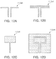
- FIGS. 12A through 12D are schematic views illustrating kinds of antenna patterns that may be used in the fan-out semiconductor package of FIG. 9 ;
- FIG. 13 is a schematic view illustrating a modified example of an antenna pattern that may be used in the fan-out semiconductor package of FIG. 9 ;
- FIGS. 14A through 14F are schematic views illustrating an example of processes of manufacturing the fan-out semiconductor package of FIG. 9 ;
- FIG. 15 is a schematic cross-sectional view illustrating another example of a fan-out semiconductor package
- FIG. 16 is a schematic plan view illustrating the fan-out semiconductor package of FIG. 15 when viewed from above;
- FIG. 17 is a schematic cross-sectional view illustrating another example of a fan-out semiconductor package
- FIG. 18 is a schematic plan view illustrating the fan-out semiconductor package of FIG. 17 when viewed from above;
- FIG. 19 is a schematic cross-sectional view illustrating another example of a fan-out semiconductor package
- FIGS. 20A through 20D are schematic plan views illustrating various examples of the fan-out semiconductor package of FIG. 19 when viewed from above;
- FIG. 21 is a schematic cross-sectional view illustrating another example of a fan-out semiconductor package
- FIG. 22 is a schematic plan view illustrating the fan-out semiconductor package of FIG. 21 when viewed from above;
- FIG. 23 is a schematic plan view illustrating the fan-out semiconductor package of FIG. 21 when viewed from below;
- FIG. 24 is a schematic cross-sectional view illustrating another example of a fan-out semiconductor package
- FIG. 25 is a schematic cross-sectional view illustrating another example of a fan-out semiconductor package
- FIG. 26 is a schematic cross-sectional view illustrating another example of a fan-out semiconductor package
- FIG. 27 is a schematic cross-sectional view illustrating another example of a fan-out semiconductor package
- FIG. 28 is a schematic cross-sectional view illustrating another example of a fan-out semiconductor package
- FIG. 29 is a schematic cross-sectional view illustrating another example of a fan-out semiconductor package
- FIG. 30 is a schematic cross-sectional view illustrating another example of a fan-out semiconductor package
- FIG. 31 is a schematic cross-sectional view illustrating another example of a fan-out semiconductor package
- FIG. 32 is a schematic cross-sectional view illustrating an example in which a fan-out semiconductor package according to the related art is applied to a main board.
- FIG. 33 is a schematic cross-sectional view illustrating an example in which a fan-out semiconductor package according to the present disclosure is applied to a main board.
- a lower side, a lower portion, a lower surface, and the like are used to refer to a direction toward a mounting surface of the fan-out semiconductor package in relation to cross sections of the drawings, while an upper side, an upper portion, an upper surface, and the like, are used to refer to an opposite direction to the direction.
- these directions are defined for convenience of explanation, and the claims are not particularly limited by the directions defined as described above.
- connection of a component to another component in the description includes an indirect connection through an adhesive layer as well as a direct connection between two components.
- electrically connected conceptually includes a physical connection and a physical disconnection. It can be understood that when an element is referred to with terms such as “first” and “second”, the element is not limited thereby. They may be used only for a purpose of distinguishing the element from the other elements, and may not limit the sequence or importance of the elements. In some cases, a first element may be referred to as a second element without departing from the scope of the claims set forth herein. Similarly, a second element may also be referred to as a first element.
- a first connection member is disposed on a level above a redistribution layer.
- a vertical direction refers to the abovementioned upward and downward directions
- a horizontal direction refers to a direction perpendicular to the abovementioned upward and downward directions.
- a vertical cross section refers to a case taken along a plane in the vertical direction, and an example thereof may be a cross-sectional view illustrated in the drawings.
- a horizontal cross section refers to a case taken along a plane in the horizontal direction, and an example thereof may be a plan view illustrated in the drawings.
- FIG. 1 is a schematic block diagram illustrating an example of an electronic device system.
- an electronic device 1000 may accommodate a mainboard 1010 therein.
- the mainboard 1010 may include chip related components 1020 , network related components 1030 , other components 1040 , and the like, physically or electrically connected thereto. These components may be connected to others to be described below to form various signal lines 1090 .
- the chip related components 1020 may include a memory chip such as a volatile memory (for example, a dynamic random access memory (DRAM)), a non-volatile memory (for example, a read only memory (ROM)), a flash memory, or the like; an application processor chip such as a central processor (for example, a central processing unit (CPU)), a graphics processor (for example, a graphics processing unit (GPU)), a digital signal processor, a cryptographic processor, a microprocessor, a microcontroller, or the like; and a logic chip such as an analog-to-digital converter (ADC), an application-specific integrated circuit (ASIC), or the like.
- the chip related components 1020 are not limited thereto, and may also include other types of chip-related components.
- the chip related components 1020 may be combined with each other.
- the network related components 1030 may include protocols such as wireless fidelity (Wi-Fi) (Institute of Electrical And Electronics Engineers (IEEE) 802.11 family, or the like), worldwide interoperability for microwave access (WiMAX) (IEEE 802.16 family, or the like), IEEE 802.20, long term evolution (LTE), evolution data only (Ev-DO), high speed packet access+(HSPA+), high speed downlink packet access+(HSDPA+), high speed uplink packet access+(HSUPA+), enhanced data GSM environment (EDGE), global system for mobile communications (GSM), global positioning system (GPS), general packet radio service (GPRS), code division multiple access (CDMA), time division multiple access (TDMA), digital enhanced cordless telecommunications (DECT), Bluetooth, 3G, 4G, and 5G protocols, and any other wireless and wired protocols, designated after the abovementioned protocols.
- Wi-Fi Institutee of Electrical And Electronics Engineers (IEEE) 802.11 family, or the like
- WiMAX worldwide interoper
- Other components 1040 may include a high frequency inductor, a ferrite inductor, a power inductor, ferrite beads, a low temperature co-firing ceramic (LTCC), an electromagnetic interference (EMI) filter, a multilayer ceramic capacitor (MLCC), and the like.
- LTCC low temperature co-firing ceramic
- EMI electromagnetic interference
- MLCC multilayer ceramic capacitor
- other components 1040 are not limited thereto, and may also include passive components used for various other purposes, and the like.
- other components 1040 may be combined with each other, together with the chip related components 1020 or the network related components 1030 described above.
- the electronic device 1000 may include other components that may or may not be physically or electrically connected to the mainboard 1010 .
- these other components may include, for example, a camera 1050 , an antenna 1060 , a display device 1070 , a battery 1080 , an audio codec (not illustrated), a video codec (not illustrated), a power amplifier (not illustrated), a compass (not illustrated), an accelerometer (not illustrated), a gyroscope (not illustrated), a speaker (not illustrated), a mass storage unit (for example, a hard disk drive) (not illustrated), a compact disk (CD) drive (not illustrated), a digital versatile disk (DVD) drive (not illustrated), or the like.
- these other components are not limited thereto, and may also include other components used for various purposes depending on a type of electronic device 1000 , or the like.
- the electronic device 1000 may be a smartphone, a personal digital assistant (PDA), a digital video camera, a digital still camera, a network system, a computer, a monitor, a tablet personal computer (PC), a laptop PC, a netbook PC, a television, a video game machine, a smartwatch, an automotive component, or the like.
- PDA personal digital assistant
- PC tablet personal computer
- netbook PC netbook PC
- television a video game machine
- smartwatch an automotive component, or the like.
- the electronic device 1000 is not limited thereto, and may be any other electronic device processing data.
- FIG. 2 is a schematic perspective view illustrating an example of an electronic device.
- a semiconductor package may be used for various purposes in the various electronic devices 1000 as described above.
- a motherboard 1110 may be accommodated in a body 1101 of a smartphone 1100 , and various components 1120 may be physically or electrically connected to the motherboard 1110 .
- other components that may or may not be physically or electrically connected to the mainboard 1010 such as a camera 1130 , may be accommodated in the body 1101 .
- Some of the electronic components 1120 may be the chip related components, and the semiconductor package 100 may be, for example, an application processor among the chip related components, but is not limited thereto.
- the electronic device is not necessarily limited to the smartphone 1100 , and may be other electronic devices as described above.
- the semiconductor chip may not serve as a finished semiconductor product in itself, and may be damaged due to external physical or chemical impacts. Therefore, the semiconductor chip itself may not be used, and may be packaged and used in an electronic device, or the like, in a packaged state.
- semiconductor packaging is required, due to the existence of a difference in a circuit width between the semiconductor chip and a mainboard of the electronic device in terms of electrical connections.
- a size of connection pads of the semiconductor chip and an interval between the connection pads of the semiconductor chip are very fine, but a size of component mounting pads of the mainboard used in the electronic device and an interval between the component mounting pads of the mainboard are significantly larger than those of the semiconductor chip. Therefore, it may be difficult to directly mount the semiconductor chip on the mainboard, and packaging technology for buffering a difference in a circuit width between the semiconductor chip and the mainboard is required.
- a semiconductor package manufactured by the packaging technology may be classified as a fan-in semiconductor package or a fan-out semiconductor package depending on a structure and a purpose thereof.
- FIGS. 3A and 3B are schematic cross-sectional views illustrating states of a fan-in semiconductor package before and after being packaged.
- FIG. 4 is a schematic cross-sectional view illustrating a packaging process of a fan-in semiconductor package.
- a semiconductor chip 2220 may be, for example, an integrated circuit (IC) in a bare state, including a body 2221 including silicon (Si), germanium (Ge), gallium arsenide (GaAs), or the like, connection pads 2222 formed on one surface of the body 2221 and including a conductive material such as aluminum (Al), or the like, and a passivation layer 2223 such as an oxide film, a nitride film, or the like, formed on one surface of the body 2221 and covering at least portions of the connection pads 2222 .
- the connection pads 2222 may be significantly small, it may be difficult to mount the integrated circuit (IC) on an intermediate level printed circuit board (PCB) as well as on the mainboard of the electronic device, or the like.
- a connection member 2240 may be formed on the semiconductor chip 2220 in order to redistribute the connection pads 2222 .
- the connection member 2240 may be formed by forming an insulating layer 2241 on the semiconductor chip 2220 using an insulating material such as photoimagable dielectric (PID) resin, forming via holes 2243 h opening the connection pads 2222 , and then forming wiring patterns 2242 and vias 2243 . Then, a passivation layer 2250 protecting the connection member 2240 may be formed, an opening 2251 may be formed, and an underbump metal layer 2260 , or the like, may be formed. That is, a fan-in semiconductor package 2200 including, for example, the semiconductor chip 2220 , the connection member 2240 , the passivation layer 2250 , and the under-bump metal layer 2260 may be manufactured through a series of processes.
- PID photoimagable dielectric
- the fan-in semiconductor package may have a package form in which all of the connection pads, for example, input/output (I/O) terminals, of the semiconductor chip, are disposed inside the semiconductor chip, and may have excellent electrical characteristics and be produced at a low cost. Therefore, many elements mounted in smartphones have been manufactured in a fan-in semiconductor package form. In detail, many elements mounted in smartphones have been developed to implement a rapid signal transfer while having a compact size.
- I/O input/output
- the fan-in semiconductor package since all I/O terminals need to be disposed inside the semiconductor chip in the fan-in semiconductor package, the fan-in semiconductor package has significant spatial limitations. Therefore, it is difficult to apply this structure to a semiconductor chip having a large number of I/O terminals or a semiconductor chip having a compact size. In addition, due to the disadvantage described above, the fan-in semiconductor package may not be directly mounted and used on the mainboard of the electronic device.
- the size of the I/O terminals of the semiconductor chip and the interval between the I/O terminals of the semiconductor chip may not be sufficient to directly mount the fan-in semiconductor package on the mainboard of the electronic device.
- FIG. 5 is a schematic cross-sectional view illustrating a case in which a fan-in semiconductor package is mounted on an interposer substrate and is ultimately mounted on a mainboard of an electronic device.
- FIG. 6 is a schematic cross-sectional view illustrating a case in which a fan-in semiconductor package is embedded in an interposer substrate and is ultimately mounted on a mainboard of an electronic device.
- connection pads 2222 that is, I/O terminals, of a semiconductor chip 2220 may be redistributed through an interposer substrate 2301 , and the fan-in semiconductor package 2200 may be ultimately mounted on a mainboard 2500 of an electronic device in a state in which it is mounted on the interposer substrate 2301 .
- solder balls 2270 and the like, may be fixed by an underfill resin 2280 , or the like, and an outer side of the semiconductor chip 2220 may be covered with a molding material 2290 , or the like.
- a fan-in semiconductor package 2200 may be embedded in a separate interposer substrate 2302 , connection pads 2222 , that is, I/O terminals, of the semiconductor chip 2220 may be redistributed by the interposer substrate 2302 in a state in which the fan-in semiconductor package 2200 is embedded in the interposer substrate 2302 , and the fan-in semiconductor package 2200 may be ultimately mounted on a mainboard 2500 of an electronic device.
- the fan-in semiconductor package may be mounted on the separate interposer substrate and be then mounted on the mainboard of the electronic device through a packaging process or may be mounted and used on the mainboard of the electronic device in a state in which it is embedded in the interposer substrate.
- FIG. 7 is a schematic cross-sectional view illustrating a fan-out semiconductor package.
- an outer side of a semiconductor chip 2120 may be protected by an encapsulant 2130 , and connection pads 2122 of the semiconductor chip 2120 may be redistributed outwardly of the semiconductor chip 2120 by a connection member 2140 .
- a passivation layer 2202 may further be formed on the connection member 2140
- an underbump metal layer 2160 may further be formed in openings of the passivation layer 2202 .
- Solder balls 2170 may further be formed on the underbump metal layer 2160 .
- the semiconductor chip 2120 may be an integrated circuit (IC) including a body 2121 , the connection pads 2122 , a passivation layer (not illustrated), and the like.
- the connection member 2140 may include an insulating layer 2141 , redistribution layers 2142 formed on the insulating layer 2141 , and vias 2143 electrically connecting the connection pads 2122 and the redistribution layers 2142 to each other.
- the fan-out semiconductor package may have a form in which I/O terminals of the semiconductor chip are redistributed and disposed outwardly of the semiconductor chip through the connection member formed on the semiconductor chip.
- the fan-in semiconductor package all I/O terminals of the semiconductor chip need to be disposed inside the semiconductor chip. Therefore, when a size of the semiconductor chip is decreased, a size and a pitch of balls need to be decreased, such that a standardized ball layout may not be used in the fan-in semiconductor package.
- the fan-out semiconductor package has the form in which the I/O terminals of the semiconductor chip are redistributed and disposed outwardly of the semiconductor chip through the connection member formed on the semiconductor chip as described above.
- a standardized ball layout may be used in the fan-out semiconductor package as it is, such that the fan-out semiconductor package may be mounted on the mainboard of the electronic device without using a separate interposer substrate, as described below.
- FIG. 8 is a schematic cross-sectional view illustrating a case in which a fan-out semiconductor package is mounted on a mainboard of an electronic device.
- a fan-out semiconductor package 2100 may be mounted on a mainboard 2500 of an electronic device through solder balls 2170 , or the like. That is, as described above, the fan-out semiconductor package 2100 includes the connection member 2140 formed on the semiconductor chip 2120 and capable of redistributing the connection pads 2122 to a fan-out region that is outside of a size of the semiconductor chip 2120 , such that the standardized ball layout may be used in the fan-out semiconductor package 2100 as it is. As a result, the fan-out semiconductor package 2100 may be mounted on the mainboard 2500 of the electronic device without using a separate interposer substrate, or the like.
- the fan-out semiconductor package may be mounted on the mainboard of the electronic device without using the separate interposer substrate, the fan-out semiconductor package may be implemented at a thickness lower than that of the fan-in semiconductor package using the interposer substrate. Therefore, the fan-out semiconductor package may be miniaturized and thinned. In addition, the fan-out semiconductor package has excellent thermal characteristics and electrical characteristics, such that it is particularly appropriate for a mobile product. Therefore, the fan-out semiconductor package may be implemented in a form more compact than that of a general package-on-package (POP) type using a printed circuit board (PCB), and may solve a problem due to the occurrence of a warpage phenomenon.
- POP general package-on-package
- PCB printed circuit board
- the fan-out semiconductor package refers to package technology for mounting the semiconductor chip on the mainboard of the electronic device, or the like, as described above, and protecting the semiconductor chip from external impacts, and is a concept different from that of a printed circuit board (PCB) such as an interposer substrate, or the like, having a scale, a purpose, and the like, different from those of the fan-out semiconductor package, and having the fan-in semiconductor package embedded therein.
- PCB printed circuit board
- FIG. 9 is a schematic cross-sectional view illustrating an example of a fan-out semiconductor package.
- FIG. 10 is a schematic plan view illustrating the fan-out semiconductor package of FIG. 9 when viewed from above.
- FIG. 11 is a schematic plan view illustrating the fan-out semiconductor package of FIG. 9 when viewed from below.
- a fan-out semiconductor package 100 A may include a core member 110 having a through-hole 110 H, a semiconductor chip 120 disposed in the through-hole 110 H and having an active surface having connection pads 120 P disposed thereon and an inactive surface opposing the active surface, an encapsulant 130 encapsulating at least portions of the core member 110 and the semiconductor chip 120 , and a connection member 140 disposed on the core member 110 and the active surface of the semiconductor chip 120 .
- the semiconductor chip 120 may be disposed in face-up form so that the active surface is directed toward the top in the drawings.
- the core member 110 may include an insulating layer 111 , wiring layers 112 a and 112 b formed on opposite surfaces of the insulating layer 111 , and vias 113 connecting the wiring layers 112 a and 112 b to each other.
- a first wiring layer 112 a of the core member 110 may include an antenna pattern 112 a A
- a second wiring layer 112 b of the core member 110 may include a ground pattern 112 b G.
- the first wiring layer 112 a may include the antenna pattern 112 a A.
- the antenna pattern 112 a A may be connected to a redistribution layer 142 through a feeding line 112 a F in a signal manner to be thus connected to the connection pads 120 P of the semiconductor chip 120 in a signal manner.
- An underbump metal layer 160 and electrical connection structures 170 may be disposed beneath the core member 110 , and the fan-out semiconductor package 100 A may thus be mounted on the main board, or the like.
- a means of implementing an antenna, a ground face, a dielectric material, a feeding line, or the like, needs to be considered, in order to determine a resonance frequency and a bandwidth of the antenna.
- a distance between the antenna and the ground face that has a sensitive influence on characteristics of the antenna, that is, a thickness of an air layer or a thickness of a dielectric material needs to be constantly maintained and managed in order to secure stable radiation characteristics of the antenna.
- a manner of forming an antenna 242 A on a redistribution layer 240 of a package 200 A and forming a ground face 302 G on a main board 300 has been used.
- a thickness or a distance d between the antenna 242 A and the ground face 302 G needs to be secured by a height of solder balls 270 of the package 200 A. Therefore, when the package 200 A is mounted on the main board 300 , a thickness difference may be generated depending on a height level in which the solder ball collapse.
- a dielectric material is used as a material of the air layer, and a size of the antenna 242 A is thus increased.
- a flux or a foreign material may be inserted into a space between the antenna 242 A and the ground face 302 G, resulting in significantly influence on characteristics of the antenna 242 A.
- a flux or a foreign material may be inserted into a space between the antenna 242 A and the ground face 302 G, resulting in significantly influence on characteristics of the antenna 242 A.
- heat is generated in the RFIC 220 , it is difficult to secure a sufficient heat dissipation path, and thus, there is a limitation in using such a manner in a product that uses a large amount of power.
- the core member 110 is introduced and the antenna pattern 112 a A and the ground pattern 112 b G are formed on and beneath the core member 110 , respectively. Therefore, even though the fan-out semiconductor package 100 A is mounted on the main board 300 , a stable design structure of the antenna pattern 112 a A, that is, a distance d 1 between the antenna pattern 112 a A and the ground pattern 112 b G may be stably secured regardless of a change in an external environment to maintain radiation characteristics of an antenna 112 a G.
- a size of the antenna pattern 112 a A may be reduced using a dielectric constant ( ⁇ 1 ) of the insulating layer 111 of the core member 110 to simplify an entire size of the fan-out semiconductor package 100 A, resulting in improvement of spatial efficiency and reduction in a cost.
- deterioration of performance of the antenna pattern 112 a A due to an influence of the foreign material in a space between the antenna pattern 112 a A and the ground pattern 112 b G may also be prevented.
- the electrical connection structures 170 are not limited to solder balls, and may be implemented in a very small thickness.
- the core member 110 may be formed on the basis of a single substrate that has large areas, respectively, on upper and lower surfaces thereof and is not separated, the antenna pattern 112 a A and the ground pattern 112 b G may be formed on and beneath the core member 110 , respectively, and the semiconductor chip 120 such as the RFIC, or the like, may then be disposed in the through-hole 110 H of the core member 110 . That is, the core member 110 may be a single member having a large area, and may not consist of a plurality of unit members. Therefore, a manufacturing process may be simple and a reduction in a cost may be possible.
- a ground surface for an antenna pattern 112 a A or various other signal patterns of the first wiring layer 112 a may be solved by the ground pattern 112 b G of the second wiring layer 112 b .
- a term “connected” herein is a concept including a case in which components are electrically connected to each other or are connected in a signal manner as well as a case in which components are physically connected to each other.
- the term ‘connected’ is a concept including an indirect connection as well as a direct connection.
- a term “electrically connected or connected in a signal manner” is a concept including a physical connection and a physical disconnection.
- the core member 110 may include the wiring layers 112 a and 112 b redistributing the connection pads 120 P of the semiconductor chip 120 to thus reduce the number of layers of the connection member 140 . If necessary, the core member 110 may improve rigidity of the fan-out semiconductor package 100 A depending on a material of the insulating layer 111 constituting the core member 110 , and secure uniformity of a thickness of the encapsulant 130 .
- the fan-out semiconductor package 100 A according to the exemplary embodiment may be utilized as a package-on-package (PoP) type package by the core member 110 . That is, the core member 110 may be used as a connection member.
- the core member 110 may have the through-hole 110 H.
- the semiconductor chip 120 may be disposed in the through-hole 110 H to be spaced apart from the core member 110 by a predetermined distance. Side portions of the semiconductor chip 120 may be surrounded by the core member 110 .
- the core member 110 may include the insulating layer 111 , the first wiring layer 112 a disposed on the insulating layer 111 , the second wiring layer 112 b disposed beneath the insulating layer 111 , and the vias 113 penetrating through the insulating layer 111 and connecting the first and second wiring layers 112 a and 112 b to each other. Thicknesses of the wiring layers 112 a and 112 b of the core member 110 may be greater than those of the redistribution layers 142 of the connection member 140 .
- the core member 110 may have a thickness similar to or greater than that of the semiconductor chip 120 , or the like, the wiring layers 112 a and 112 b may be formed at large sizes through a substrate process depending on a scale of the core member 110 .
- the redistribution layers 142 of the connection member 140 may be formed at small sizes through a semiconductor process for thinness.
- a material of the insulating layer 111 is not particularly limited.
- an insulating material may be used as the material of the insulating layer 111 .
- the insulating material may be a thermosetting resin such as an epoxy resin, a thermoplastic resin such as a polyimide resin, a resin in which the thermosetting resin or the thermoplastic resin is impregnated together with an inorganic filler in a core material such as a glass fiber (or a glass cloth or a glass fabric), for example, prepreg, Ajinomoto Build up Film (ABF), FR-4, Bismaleimide Triazine (BT), or the like.
- ABS Ajinomoto Build up Film
- FR-4 Bismaleimide Triazine
- the wiring layers 112 a and 112 b may redistribute the connection pads 120 P of the semiconductor chip 120 .
- the wiring layers 112 a and 112 b may include a specific pattern such as the antenna pattern 112 a A.
- a material of each of the wiring layers 112 a and 112 b may be a conductive material such as copper (Cu), aluminum (Al), silver (Ag), tin (Sn), gold (Au), nickel (Ni), lead (Pb), titanium (Ti), or alloys thereof.
- the wiring layers 112 a and 112 b may perform various functions depending on designs of their corresponding layers.
- the wiring layers 112 a and 112 b may include ground (GND) patterns, power (PWR) patterns, signal (S) patterns, and the like.
- the signal (S) patterns may include various signals except for the ground (GND) patterns, the power (PWR) patterns, and the like, such as data signals, frequency signals, and the like.
- the wiring layers 112 a and 112 b may include various pad patterns, and the like.
- the first wiring layer 112 a may include the antenna pattern 112 a A and the feeding line 112 a F connecting the antenna pattern 112 a A to the connection pads 120 P of the semiconductor chip 120 , or the like.
- the antenna pattern 112 a A may be connected to connection pads 120 PS for a signal of the connection pads 120 P through signal patterns 142 S of the redistribution layer 142 in a signal manner.
- the first wiring layer 112 a may further include a ground pattern 112 a G having a plate shape, pads 112 a PG for a ground connection, pads 112 a PS for a signal connection, and the like.
- the second wiring layer 112 b may include the ground pattern 112 b G.
- the ground pattern 112 b G may be connected to connection pads 120 PG for a ground of the connection pads 120 P through a ground pattern 142 G of the redistribution layer 142 .
- the ground pattern 112 b G may be formed in a plate shape, and may occupy most of a lower surface of the insulating layer 111 .
- the ground pattern 112 b G may serve as a ground of the antenna pattern 112 a A, the semiconductor chip 120 , various signal patterns, and the like.
- the second wiring layer 112 b may include electrical connection structure pads 112 b PS for a signal connection, electrical connection structure pads 112 b PG for a ground connection, and the like, in addition to the ground pattern 112 b G.
- the fan-out semiconductor package 100 A may have the antenna pattern 112 a A and the ground patterns 112 b G disposed on opposite surfaces of the core member 110 . Therefore, a distance between the antenna pattern 112 a A and the ground pattern 112 b G may be stably secured to maintain radiation characteristics of the antenna 112 a G, and the size of the antenna pattern 112 a A may be reduced using the dielectric constant of a dielectric in the core member 110 , that is, the insulating layer 111 , to simplify the entire size of the fan-out semiconductor package 100 A, resulting in improvement of spatial efficiency and reduction in a cost.
- the electrical connection structures 170 are not limited to solder balls, and may be thinned.
- the vias 113 may connect the wiring layers 112 a and 112 b formed on different layers to each other, resulting in an electrical path in the core member 110 .
- the vias 113 may include vias 113 S for a signal connection, vias 113 G for a ground connection, and the like.
- a material of each of the vias 113 may be a conductive material such as copper (Cu), aluminum (Al), silver (Ag), tin (Sn), gold (Au), nickel (Ni), lead (Pb), titanium (Ti), or alloys thereof.
- Each of the vias 113 may be completely filled with the conductive material, or the conductive material may be formed along a wall of each of via holes.
- each of the vias 113 may have any known shape such as a sandglass shape, a cylindrical shape, and the like.
- the semiconductor chip 120 may be an integrated circuit (IC) in a bare state, provided in an amount of several hundreds to several millions of elements or more integrated in a single chip.
- the integrated circuit (IC) may be, for example, a radio frequency integrated circuit (RFIC). That is, the fan-out semiconductor package 100 A according to the exemplary embodiment may be a package in which the RFIC and a millimeter wave/5G antenna are integrated with each other.
- the semiconductor chip 120 may include a body on which various circuits are formed, and the connection pads 120 P may be formed on an active surface of the body. The body may be formed on the basis of, for example, an active wafer.
- connection pads 120 P may connect the semiconductor chip 120 to other components, and a material of each of the connection pads 120 P may be a conductive material such as aluminum (Al), but is not limited thereto.
- the active surface of the semiconductor chip 120 refers to a surface of the semiconductor chip 120 on which the connection pads 120 P are disposed, and the inactive surface of the semiconductor chip 120 refers to a surface of the semiconductor chip 120 opposing the active surface.
- the semiconductor chip 120 may be disposed in face-up form so that the active surface thereof is directed toward the top.
- the connection member 140 may also be disposed on the core member 110 .
- the first wiring layer 112 a may be formed on a level above the second wiring layer 112 b .
- connection pads 120 PS for a signal of the connection pads 120 P of the semiconductor chip 120 may be connected to the feeding line 112 a F of the antenna pattern 112 a A through a redistribution layer 142 S for a signal and vias 143 S of the connection member 140 . Resultantly, a distance from the connection pads 120 PS for a signal to the feeding line 112 a F of the antenna pattern 112 a A may be significantly reduced. Therefore, low insertion loss may be implemented.
- the encapsulant 130 may be configured to protect the semiconductor chip 120 and provide an insulation region.
- An encapsulation form of the encapsulant 130 is not particularly limited, and may be a form in which the encapsulant 130 surrounds at least portions of the semiconductor chip 120 .
- the encapsulant 130 may cover a lower surface of the core member 110 , and cover side surface and the inactive surface of the semiconductor chip 120 .
- the encapsulant 130 may fill at least portions of the through-hole 110 H.
- the certain materials of the encapsulant 130 are not particularly limited, but may be an insulating material such as ABF. Alternatively, a photoimagable encapsulant (PIE) may be used as the material of the encapsulant 130 .
- PIE photoimagable encapsulant
- connection member 140 may serve to connect the fan-out semiconductor package 100 A according to the exemplary embodiment to an external component.
- the connection member 140 may redistribute the connection pads 120 P of the semiconductor chip 120 .
- the connection member 140 may include a first insulating layer 141 a , a redistribution layer 142 formed on the first insulating layer 141 a , vias 143 formed in the first insulating layer 141 a and connecting the redistribution layer 142 to patterns formed on another layer, and a second insulating layer 141 b disposed on the first insulating layer 141 a and covering the redistribution layer 142 .
- a material of the first insulating layer 141 a may be an insulating material.
- the insulating material may be a photosensitive insulating material such as a PID resin.
- the first insulating layer 141 a may be formed to have a smaller thickness, and a fine pitch of the vias 143 may be achieved more easily.
- materials of the first insulating layers 141 a may be the same as each other, and may also be different from each other, if necessary.
- the first insulating layers 141 a are the multiple layers, the first insulating layers 141 a may be integrated with each other depending on a process, such that a boundary therebetween may also not be apparent.
- a material of the second insulating layer 141 b may also be an insulating material.
- the insulating material may be ABF, or the like. That is, the outermost layer of the connection member 140 may be a passivation layer.
- the redistribution layer 142 may serve to redistribute the connection pads 120 P of the semiconductor chip 120 , and a material of the redistribution layer 142 may be a conductive material such as copper (Cu), aluminum (Al), silver (Ag), tin (Sn), gold (Au), nickel (Ni), lead (Pb), titanium (Ti), or alloys thereof.
- the redistribution layer 142 may perform various functions depending on a design of a corresponding layer.
- the redistribution layer 142 may include ground lines 142 G, signal lines 142 S, and the like.
- the redistribution layer 142 may include pads 142 PG for a ground, pads 142 PS for a signal, and the like.
- the vias 143 may connect the redistribution layer 142 , the wiring layer 112 a , and the like, formed on different layers to each other, resulting in an electrical path in the connection member 140 .
- a material of each of the vias 143 may be a conductive material such as copper (Cu), aluminum (Al), silver (Ag), tin (Sn), gold (Au), nickel (Ni), lead (Pb), titanium (Ti), or alloys thereof.
- the each of vias 143 may be completely filled with the conductive material, or the conductive material may also be formed along a wall of each of the vias.
- each of the vias 143 may have any known shape such as a tapered shape, a cylindrical shape, and the like.
- the vias 143 may also include vias 143 G for a ground, vias 143 S for a signal, and the like.
- the underbump metal layer 160 may be additionally configured to improve connection reliability of the electrical connection structures 170 to improve board level reliability of the fan-out semiconductor package 100 A.
- the underbump metal layer 160 may be connected to various pads 112 a PG and 112 a PS for electrical connection structures, of the first wiring layer 112 a of the connection member 140 exposed through openings of the encapsulant 130 .
- the underbump metal layer 160 may be formed in the openings of the encapsulant 130 by the known metallization method using the known conductive material such as a metal, but is not limited thereto.
- the electrical connection structures 170 may be additionally configured to physically or electrically externally connect the fan-out semiconductor package 100 A.
- the fan-out semiconductor package 100 A may be mounted on the main board of the electronic device through the electrical connection structures 170 .
- Each of the electrical connection structures 170 may be formed of a low melting point metal, for example, a solder formed of tin (Sn)-aluminum (Al)-copper (Cu) alloys, or the like. However, this is only an example, and a material of each of the electrical connection structures 170 is not limited thereto.
- Each of the electrical connection structures 170 may be a land, a ball, a pin, or the like.
- the electrical connection structures 170 may be formed as a multilayer or single layer structure.
- the electrical connection structures 170 may include a copper (Cu) pillar and a solder.
- the electrical connection structures 170 may include a tin-silver solder or copper (Cu).
- Cu copper
- the electrical connection structures 170 are not limited thereto.
- the number, an interval, a disposition form, and the like, of electrical connection structures 170 are not particularly limited, but may be sufficiently modified depending on design particulars by those skilled in the art.
- the electrical connection structures 170 may be provided in an amount of several tens to several millions according to the number of connection pads 120 P, or may be provided in an amount of several tens to several millions or more or several tens to several millions or less.
- At least one of the electrical connection structures 170 may be disposed in a fan-out region.
- the fan-out region refers to a region except for a region in which the semiconductor chip 120 is disposed.
- the fan-out package may have excellent reliability as compared to a fan-in package, may implement a plurality of input/output (I/O) terminals, and may facilitate a 3D interconnection.
- I/O input/output
- the fan-out package may be manufactured to have a small thickness, and may have price competitiveness.
- FIGS. 12A through 12D are schematic views illustrating kinds of antenna patterns that may be used in the fan-out semiconductor package of FIG. 9 .
- an antenna pattern 112 a A may be a dipole antenna as illustrated in FIG. 12 a , a folded dipole antenna as illustrated in FIG. 12B , a patch antenna illustrated in FIG. 12C , or a coplanar patch antenna as illustrated in FIG. 12D .
- the antenna pattern is not limited thereto, but may be a ring antenna, a loop antenna, or the like, and the respective antennas may have various shapes such as a rectangular shape, a square shape, a circular shape, a radial shape, and the like. That is, the antenna pattern 112 a A may implement millimeter wave/5G, and a kind or a type of antenna pattern 112 a A is not limited.
- FIG. 13 is a schematic view illustrating a modified example of an antenna pattern that may be used in the fan-out semiconductor package of FIG. 9 .
- an antenna pattern 112 a A may include a plurality of patch antennas 112 a A 1 , 112 a A 2 , 112 a A 3 , and 112 a A 4 .
- the respective patch antennas 112 a A 1 to 112 a A 4 may be connected to the respective connection pads of a semiconductor chip 120 for a signal through the respective feeding lines 112 a F 1 , 112 a F 2 , 112 a F 3 , and 112 a F 4 in a signal manner.
- the respective patch antennas 112 a A 1 , 112 a A 2 , 112 a A 3 , and 112 a A 4 may include transmit (Tx) antennas and receive (Rx) antennas of which the numbers are not particularly limited.
- FIGS. 14A through 14F are schematic views illustrating an example of processes of manufacturing the fan-out semiconductor package of FIG. 9 .
- the core member 110 may be prepared.
- the core member 110 may be prepared using a single large area substrate such as a copper clad laminate (CCL). That is, the core member 110 may be prepared by forming the first wiring layer 112 a and the second wiring layer 112 b on opposite surfaces of the insulating layer 111 , respectively, using the CCL and forming the vias 113 penetrating through the insulating layer 111 .
- the antenna pattern 112 a A, the feeding line 112 a F, various pads 112 a PS and 112 a PG, and the like may be formed.
- the ground pattern 112 b G, various pads 112 b PS, 112 b PG, and the like, may be formed.
- the vias 113 the vias 113 G for a ground connection, the vias 113 S for a signal connection, and the like, may be formed.
- patterns, pads, vias, and the like, for power may be formed.
- the wiring layers 112 a and 112 b may be formed by the known plating process, and the vias 113 may be formed by forming via holes with a laser drill, or the like, and then filling the via holes by plating.
- the through-hole 110 H may be formed in the core member 110 .
- the through-hole 110 H may be formed using a mechanical drill, a laser drill, or the like. In this case, a desmear process may be performed as a subsequent process.
- the through-hole 110 H may be formed by a sand blast method, or the like.
- the through-hole 110 H may penetrate between upper and lower surface of the insulating layer 111 .
- a size of the through-hole 110 H may be appropriately designed depending on a size of the semiconductor chip 120 .
- the metal layer may be formed on the walls of the through-hole 110 H and be then connected to the ground, as described below. In this case, the metal layer may also be used as the ground.
- the semiconductor chip 120 may be disposed using an adhesive film 190 , and may be encapsulated by the encapsulant 130 .
- the core member 110 in which the through-hole 110 H is formed may be attached to the adhesive film 190 such as a tape, or the like, so that the first wiring layer 112 a is directed toward the adhesive film 190 , the semiconductor chip 120 may be attached to the adhesive film 190 exposed through the through-hole 110 H so that the active surface of the semiconductor chip 120 is directed toward the adhesive film 190 , and the semiconductor chip 120 may thus be encapsulated by the encapsulant 130 .
- the encapsulant 130 may be formed by stacking a film in a b-stage and then hardening the film or be formed by applying a liquid-phase material for forming the encapsulant 130 by the known coating method and then hardening the liquid-phase material.
- the adhesive film 190 may be removed, and the first insulating layer 141 a may be formed on a surface of the core member 110 on which the first wiring layer 112 a is formed and the active surface of the semiconductor chip 120 .
- the first insulating layer 141 a may be formed by stacking a PID in a b-stage and then hardening the PID or be formed by applying a material for forming a PID and then hardening the material. This process may be performed in a state in which the encapsulant 130 is attached to a carrier film 195 such as DCF, or the like.
- the redistribution layer 142 and the vias 143 may be formed on and in the first insulating layer 141 a , and the second insulating layer 141 b may be formed on the first insulating layer 141 a and the redistribution layer 142 to form the connection member 140 .
- the redistribution layer 142 may include the signal lines 142 S, the ground lines 142 G, the pads 142 PS for a signal, the pads 142 PG for a ground, and the like.
- the vias 143 may also include the vias 143 S for a signal, the vias 143 G for a ground, and the like.
- the redistribution layer 142 may be formed by the known plating process, and the vias 143 may be formed by forming via holes by a photolithography method and then filling the via holes by plating.
- the carrier film 195 may be removed, and the underbump metal layer 160 and the electrical connection structures 170 may be formed.
- the encapsulant 130 may be opened by a laser beam, or the like, to open various pads 112 a PG and 112 a PS of the second wiring 112 b of the core member 110 , and the underbump metal layer 160 and the electrical connection structures 170 may be sequentially formed.
- a plurality of fan-out semiconductor packages 100 A may be formed through a single large area substrate by a series of process, and when the plurality of fan-out semiconductor packages 100 A are sawed and separated from one another by a dicing process, the plurality of fan-out semiconductor packages 100 A may be manufactured by performing processes one time.
- FIG. 15 is a schematic cross-sectional view illustrating another example of a fan-out semiconductor package.
- FIG. 16 is a schematic plan view illustrating the fan-out semiconductor package of FIG. 15 when viewed from above.
- a fan-out semiconductor package 100 B may further include a metal layer 115 disposed on walls of a through-hole 110 H.
- the metal layer 115 may include a conductive material such as copper (Cu), aluminum (Al), silver (Ag), tin (Sn), gold (Au), nickel (Ni), lead (Pb), titanium (Ti), or alloys thereof.
- the metal layer 115 may be connected to a ground pattern 112 b G of a second wiring layer 112 b to be thus used as a ground.
- the metal layer 115 may also be connected to the ground pattern 112 a G.
- the metal layer 115 is formed on the walls of the through-hole 110 of a core member 110 using a single large area substrate, the metal layer 115 may seamlessly surround side portions of a semiconductor chip 120 , and a heat dissipation effect and an electromagnetic wave blocking effect may thus be excellent.
- processes of manufacturing the fan-out semiconductor package 100 B according to another exemplary embodiment are substantially the same as those of manufacturing the fan-out semiconductor package 100 A according to the exemplary embodiment described above except that the metal layer 115 is formed on the walls of the through-hole 110 H by the plating, and a detailed description thereof is thus omitted.
- FIG. 17 is a schematic cross-sectional view illustrating another example of a fan-out semiconductor package.
- FIG. 18 is a schematic plan view illustrating the fan-out semiconductor package of FIG. 17 when viewed from above.
- a first wiring layer 112 a of a core member 110 may include filter patterns 112 a R.
- the filter patterns 112 a R may be a strip type, a microstrip type, or the like, but are not limited thereto.
- the filter pattern 112 a R may have one end connected to a connection pad 120 PS for a signal of connection pads 120 P of a semiconductor chip 120 and the other end connected to a feeding line 112 a F of an antenna pattern 112 a A.
- connection pad 120 PS for a signal and the feeding line 112 a F may be connected to each other through the filter pattern 112 a R in a signal manner, resulting in removal of various types of noise.
- the filter patterns 112 a R and the feeding line 112 a F may be coplanar with each other, and be thus connected to each other by only a pattern without using a separate via.
- a ground pattern 112 b G of a second wiring layer 112 b may serve as a ground for the filter patterns 112 a R.
- processes of manufacturing the fan-out semiconductor package 100 C according to another exemplary embodiment are substantially the same as those of manufacturing the fan-out semiconductor package 100 A according to the exemplary embodiment described above except that the filter patterns 112 a R are formed when the first wiring layer 112 a is formed, and a detailed description thereof is thus omitted.
- the metal layer 115 described in the fan-out semiconductor package 100 B according to another exemplary embodiment may also be applied to the fan-out semiconductor package 100 C according to another exemplary embodiment.
- FIG. 19 is a schematic cross-sectional view illustrating another example of a fan-out semiconductor package.
- FIGS. 20A through 20D are schematic plan views illustrating various examples of the fan-out semiconductor package of FIG. 19 when viewed from above.
- an antenna pattern may include receive (Rx) antennas and transmit (Tx) antennas, and the receive (Rx) antennas and the transmit (Tx) antennas may be separated from each other. For example, as illustrated in FIG.
- a transmit antenna 112 a A- 1 may be disposed at the left in relation to a semiconductor chip 120
- a receive antenna 112 a A- 2 may be disposed at the right in relation to the semiconductor chip 120
- the transmit antenna 112 a A- 1 and the receive antenna 112 a A- 2 may be connected to the semiconductor chip 120 through feeding lines 112 a F- 1 and 112 a F- 2 , respectively, in a signal manner.
- a receive antenna 112 a A- 1 may be disposed at the right in relation to a semiconductor chip 120
- transmit antennas 112 a A- 2 a and 112 a A- 2 b may be disposed above and below the semiconductor chip 120 , respectively
- the receive antenna 112 a A- 1 and the transmit antennas 112 a A- 2 a and 112 a A- 2 b may be connected to the semiconductor chip 120 through feeding lines 112 a F- 1 , 112 a F- 2 a , and 112 a F- 2 b , respectively, in a signal manner.
- transmit antennas 112 a A- 1 a and 112 a A- 1 b may be disposed at the left and the right in relation to a semiconductor chip 120 , respectively, receive antennas 112 a A- 2 a and 112 a A- 2 b may be disposed above and below the semiconductor chip 120 , respectively, and the transmit antennas 112 a A- 1 a and 112 a A- 1 b and the receive antennas 112 a A- 2 a and 112 a A- 2 b may be connected to the semiconductor chip 120 through feeding lines 112 a F- 1 a , 112 a F- 1 b , 112 a F- 2 a , and 112 a F- 2 b , respectively, in a signal manner.
- transmit antennas 112 a A- 1 a and 112 a A- 1 b may be disposed at a left upper corner and a right upper corner in relation to a semiconductor chip 120 , respectively, receive antennas 112 a A- 2 a and 112 a A- 2 b may be disposed at a left lower corner and a right lower corner with respect to the semiconductor chip 120 , respectively, and the transmit antennas 112 a A- 1 a and 112 a A- 1 b and the receive antennas 112 a A- 2 a and 112 a A- 2 b may be connected to the semiconductor chip 120 through feeding lines 112 a F- 1 a , 112 a F- 1 b , 112 a F- 2 a , and 112 a F- 2 b , respectively, in a signal manner. That is, the transmit (Tx) antennas and the receive (Rx) antennas may be disposed in various forms.
- processes of manufacturing the fan-out semiconductor package 100 D according to another exemplary embodiment are substantially the same as those of manufacturing the fan-out semiconductor package 100 A according to the exemplary embodiment described above except that the antenna pattern is formed in various forms when the first wiring layer 112 a is formed, and a detailed description thereof is thus omitted.
- the metal layer 115 described in the fan-out semiconductor package 100 B according to another exemplary embodiment or the filter patterns 112 a R described in the fan-out semiconductor package 100 C according to another exemplary embodiment may also be applied to the fan-out semiconductor package 100 D according to another exemplary embodiment.
- FIG. 21 is a schematic cross-sectional view illustrating another example of a fan-out semiconductor package.
- FIG. 22 is a schematic plan view illustrating the fan-out semiconductor package of FIG. 21 when viewed from above.
- FIG. 23 is a schematic plan view illustrating the fan-out semiconductor package of FIG. 21 when viewed from below.
- a semiconductor chip 120 may be disposed in face-down form.
- a connection member 140 may be disposed beneath a core member 110 , and an underbump metal layer 160 and electrical connection structures 170 may be formed beneath the connection member 140 to be connected to a redistribution layer 142 of the connection member 140 .
- a second wiring layer 112 b of the core member 110 may be disposed on a level above a first wiring layer 112 a of the core member 110 , the first wiring layer 112 a may include a ground pattern 112 a G, the second wiring layer 112 b may include an antenna pattern 112 b A and a feeding line 112 b F, and a via 113 may include a feeding line 113 F.
- a connection pad 120 PS for a signal of the semiconductor chip 120 and the antenna pattern 112 b A may be connected to each other through a redistribution layer 142 S for a signal and a via 143 S for a signal of the connection member 140 and a via pad 112 b PS for a signal of the second wiring layer 112 b and the feeding line 113 F of the via 113 of the core member 110 in a signal manner, such that a path may become somewhat long, but heat may be easily transferred to the main board, or the like, via the connection member 140 through the active surface of the semiconductor chip 120 , and heat dissipation characteristics may thus be more excellent.
- processes of manufacturing the fan-out semiconductor package 100 E according to another exemplary embodiment are substantially the same as those of manufacturing the fan-out semiconductor package 100 A according to the exemplary embodiment described above except that the underbump metal layer 160 and the electrical connection structures 170 are formed on an opposite surface to a surface in which the underbump metal layer 160 and the electrical connection structures 170 are formed in the fan-out semiconductor package 100 A according to the exemplary embodiment so that the semiconductor chip 120 is disposed in the face-down form, and a detailed description thereof is thus omitted.
- FIG. 24 is a schematic cross-sectional view illustrating another example of a fan-out semiconductor package.
- a fan-out semiconductor package 100 F may be substantially the same as the fan-out semiconductor package 100 E according to another exemplary embodiment described above except that it further includes a metal layer 115 disposed on walls of a through-hole 110 H,
- the metal layer 115 may include a conductive material such as copper (Cu), aluminum (Al), silver (Ag), tin (Sn), gold (Au), nickel (Ni), lead (Pb), titanium (Ti), or alloys thereof.
- the metal layer 115 may be connected to a ground pattern 112 a G of a first wiring layer 112 a to be thus used as a ground.
- the metal layer 115 may also be connected to the ground pattern 112 b G. Since the metal layer 115 is formed on the walls of the through-hole 110 of a core member 110 using a single large area substrate, the metal layer 115 may seamlessly surround side portions of a semiconductor chip 120 , and a heat dissipation effect or an electromagnetic wave blocking effect may thus be excellent.
- processes of manufacturing the fan-out semiconductor package 100 F according to another exemplary embodiment are substantially the same as those of manufacturing the fan-out semiconductor package 100 A according to the exemplary embodiment described above except that the metal layer 115 is formed on the walls of the through-hole 110 H by plating and an underbump metal layer 160 and electrical connection structures 170 are formed on an opposite surface to a surface in which the underbump metal layer 160 and the electrical connection structures 170 are formed in the fan-out semiconductor package 100 A according to the exemplary embodiment so that the semiconductor chip 120 is disposed in face-down form, and a detailed description thereof is thus omitted.
- FIG. 25 is a schematic cross-sectional view illustrating another example of a fan-out semiconductor package.
- a fan-out semiconductor package 100 G may be substantially the same as the fan-out semiconductor package 100 E according to another exemplary embodiment described above except that a first wiring layer 112 a of a core member 110 includes filter patterns 112 a R.
- a metal layer 115 may be further disposed.
- the filter patterns 112 a R may be a strip type, a microstrip type, or the like, but are not limited thereto.
- the filter pattern 112 a R may have one end connected to a connection pad 120 PS for a signal of connection pads 120 P of a semiconductor chip 120 and the other end connected to a feeding line 112 b F of an antenna pattern 112 b A.
- connection pad 120 PS for a signal and the feeding line 112 b F may be connected to each other through the filter pattern 112 a R in a signal manner, resulting in removal of various noise.
- a via 113 may include a feeding line 113 F.
- the second wiring layer 112 b may include a ground pattern 112 b G for the filter pattern 112 a R.
- processes of manufacturing the fan-out semiconductor package 100 G according to another exemplary embodiment are substantially the same as those of manufacturing the fan-out semiconductor package 100 A according to the exemplary embodiment described above except that the metal layer 115 is formed on walls of a through-hole 110 H by plating, the filter patterns 112 a R are formed when the first wiring layer 112 a is formed, and an underbump metal layer 160 and electrical connection structures 170 are formed on an opposite surface to a surface in which the underbump metal layer 160 and the electrical connection structures 170 are formed in the fan-out semiconductor package 100 A according to the exemplary embodiment so that the semiconductor chip 120 is disposed in face-down form, and a detailed description thereof is thus omitted.
- FIG. 26 is a schematic cross-sectional view illustrating another example of a fan-out semiconductor package.
- a fan-out semiconductor package 100 H may be substantially the same as the fan-out semiconductor package 100 E according to another exemplary embodiment described above except that a second wiring layer 112 b of a core member 110 includes filter patterns 112 b R.
- a metal layer 115 may be further disposed.
- the filter patterns 112 b R may be a strip type, a microstrip type, or the like, but are not limited thereto.
- the filter pattern 112 b R may have one end connected to a connection pad 120 PS for a signal of connection pads 120 P of a semiconductor chip 120 and the other end connected to a feeding line 112 b F of an antenna pattern 112 b A.
- connection pad 120 PS for a signal and the feeding line 112 b F may be connected to each other through the filter pattern 112 b R in a signal manner, resulting in removal of various noise.
- a via 113 may include a feeding line 113 F.
- the filter patterns 112 b R and the feeding line 112 b F may be coplanar with each other, and be thus connected to each other by only a pattern without using a separate via.
- a ground pattern 112 a G may also provide a ground for the filter patterns 112 b R.
- processes of manufacturing the fan-out semiconductor package 100 H according to another exemplary embodiment are substantially the same as those of manufacturing the fan-out semiconductor package 100 A according to the exemplary embodiment described above except that the metal layer 115 is formed on walls of a through-hole 110 H by plating, the filter patterns 112 b R are formed when the second wiring layer 112 b is formed, and an underbump metal layer 160 and electrical connection structures 170 are formed on an opposite surface to a surface in which the underbump metal layer 160 and the electrical connection structures 170 are formed in the fan-out semiconductor package 100 A according to the exemplary embodiment so that the semiconductor chip 120 is disposed in face-down form, and a detailed description thereof is thus omitted.
- FIG. 27 is a schematic cross-sectional view illustrating another example of a fan-out semiconductor package.
- a fan-out semiconductor package 100 I may be substantially the same as the fan-out semiconductor package 100 E according to another exemplary embodiment described above except that an antenna pattern includes receive (Rx) antennas and transmit (Tx) antennas and the receive (Rx) antennas and the transmit (Tx) antennas are separated from each other.
- a transmit antenna 112 b A- 1 may be disposed at the left in relation to a semiconductor chip 120
- a receive antenna 112 b A- 2 may be disposed at the right in relation to the semiconductor chip 120
- the transmit antenna 112 b A- 1 and the receive antenna 112 b A- 2 may be connected to the semiconductor chip 120 through feeding lines 112 b F 1 and 112 b F 2 , respectively, in a signal manner.
- the transmit antennas and the receive antennas may be disposed in the forms described in the fan-out semiconductor package 100 D according to another exemplary embodiment described above. That is, the transmit (Tx) antennas and the receive (Rx) antennas may be disposed in various forms.
- processes of manufacturing the fan-out semiconductor package 100 I according to another exemplary embodiment are substantially the same as those of manufacturing the fan-out semiconductor package 100 A according to the exemplary embodiment described above except that the antenna patterns 112 b A- 1 and 112 b A- 2 are formed in various forms when the second wiring layer 112 b is formed and an underbump metal layer 160 and electrical connection structures 170 are formed on an opposite surface to a surface in which the underbump metal layer 160 and the electrical connection structures 170 are formed in the fan-out semiconductor package 100 A according to the exemplary embodiment so that the semiconductor chip 120 is disposed in face-down form, and a detailed description thereof is thus omitted.
- the metal layer 115 described in the fan-out semiconductor package 100 F according to another exemplary embodiment or the filter patterns 112 a R or 112 b R described in the fan-out semiconductor package 100 G or 100 H according to another exemplary embodiment may also be applied to the fan-out semiconductor package 100 I according to another exemplary embodiment.
- FIG. 28 is a schematic cross-sectional view illustrating another example of a fan-out semiconductor package.
- a fan-out semiconductor package 100 J may be substantially the same as the fan-out semiconductor package 100 E according to another exemplary embodiment described above except that a core member 110 includes a first insulating layer 111 a , a first wiring layer 112 a embedded in the first insulating layer 111 a so that a lower surface thereof is exposed, a second wiring layer 112 b disposed on the other surface of the first insulating layer 111 a opposing one surface of the first insulating layer 111 a on which the first wiring layer 112 a is disposed, a second insulating layer 111 b disposed on the first insulating layer 111 a and covering the second wiring layer 112 b , and a third wiring layer 112 c disposed on the second insulating layer 111 b .
- the first to third wiring layers 112 a , 112 b , and 112 c may be electrically connected to each other through first and second vias 113 a and 113 b each penetrating through the first to third insulating layers 111 a and 111 b .
- a lower surface of the first wiring layer 112 a may have a step with respect to a lower surface of the first insulating layer 111 a .
- an insulating distance of a connection member 140 may become more constant, and a phenomenon in which an encapsulant 130 bleeds may be prevented to some degree.
- the first to third wiring layers 112 a , 112 b , and 112 c may have thicknesses greater than that of a redistribution layer 142 .
- the first wiring layer 112 a may include a filter pattern 112 a R
- the second wiring layer 112 b may include a ground pattern 112 b G
- the third wiring layer 112 c may include an antenna pattern 112 c A.
- the first and second vias 113 a and 113 b may provide feeding lines 113 a F and 113 b F, respectively.
- the ground pattern 112 b G may be a ground for the antenna pattern 112 c A and the filter pattern 112 a R.
- the antenna pattern 112 c A, the ground pattern 112 b G, and the filter pattern 112 a R may be disposed in various forms.
- an appropriate combination of a material having high dielectric constant (Er 1 ) characteristics for reducing a size of an antenna and a material having low dielectric constant (Er 2 ) characteristics for reducing loss of a filter may be used as materials of the first and second insulating layers 111 a and 111 b.
- processes of manufacturing the fan-out semiconductor package 100 J according to another exemplary embodiment are substantially the same as those of manufacturing the fan-out semiconductor package 100 A according to the exemplary embodiment described above except that the core member 110 is manufactured by a coreless method, an underbump metal layer 160 and electrical connection structures 170 are formed on an opposite surface to a surface in which the underbump metal layer 160 and the electrical connection structures 170 are formed in the fan-out semiconductor package 100 A according to the exemplary embodiment so that a semiconductor chip 120 is disposed in face-down form, and a metal layer 115 , the filter pattern 112 a R, and the like, are further formed, and a detailed description thereof is thus omitted.
- the metal layer 115 described in the fan-out semiconductor package 100 F according to another exemplary embodiment may also be applied to the fan-out semiconductor package 100 J according to another exemplary embodiment.
- FIG. 29 is a schematic cross-sectional view illustrating another example of a fan-out semiconductor package.
- a fan-out semiconductor package 100 K may be substantially the same as the fan-out semiconductor package 100 E according to another exemplary embodiment described above except that a core member 110 may include a first insulating layer 111 a , a first wiring layer 112 a disposed beneath the first insulating layer 111 a , a second wiring layer 112 b disposed on the first insulating layer 111 a , a second insulating layer 111 b disposed on the first insulating layer 111 a and covering the first wiring layer 112 a , a third wiring layer 112 c disposed on the second insulating layer 111 b , a third insulating layer 111 c disposed on the first insulating layer 111 a and covering the second wiring layer 112 b , and a fourth wiring layer 112 d disposed on the third insulating layer 111 c .
- the first to fourth wiring layers 112 a , 112 b , 112 c , and 112 d may be electrically connected to each other through first to third vias 113 a , 113 b , and 113 c penetrating through the first to third insulating layers 111 a , 111 b , and 111 c , respectively.
- the first insulating layer 111 a may have a thickness greater than those of the second and third insulating layers 111 b and 111 c .
- the first insulating layer 111 a may have an elastic modulus greater than those of the second and third insulating layers 111 b and 111 c .
- the first insulating layer 111 a may include prepreg, and the second and third insulating layers 111 b and 111 c may include ABF.
- the materials of the first insulating 111 a and the second and third insulating layers 111 b and 111 c are not limited thereto.
- the first to fourth wiring layers 112 a , 112 b , 112 c , and 112 d may have thicknesses greater than that of a redistribution layer 142 .
- the first wiring layer 112 a may include a filter pattern 112 a R
- the second wiring layer 112 b may include a ground pattern 112 b G
- the third wiring layer 112 c may include a ground pattern 112 c G
- the fourth wiring layer 112 d may include an antenna pattern 112 d A.
- the first and third vias 113 a and 113 c may provide feeding lines 113 a F and 113 c F, respectively.
- the ground pattern 112 b G may be a ground of the antenna pattern 112 d A and the filter pattern 112 a R.
- the ground pattern 112 c G may be a ground of the filter pattern 112 a R.
- the antenna pattern 112 d A, the ground patterns 112 b G and 112 c G, and the filter pattern 112 a R may be disposed in various forms. Meanwhile, an appropriate combination of a material having high dielectric constant (Er 1 ) characteristics for reducing a size of an antenna and a material having low dielectric constant (Er 2 ) characteristics for reducing loss of a filter may be used as materials of the first to third insulating layers 111 a , 111 b , and 111 c.
- Er 1 dielectric constant
- Er 2 low dielectric constant
- processes of manufacturing the fan-out semiconductor package 100 K according to another exemplary embodiment are substantially the same as those of manufacturing the fan-out semiconductor package 100 A according to the exemplary embodiment described above except that a larger number of wiring layers 112 c and 112 d are formed using ABF, or the like, as a build-up layer when the core member 110 is formed, an underbump metal layer 160 and electrical connection structures 170 are formed on an opposite surface to a surface in which the underbump metal layer 160 and the electrical connection structures 170 are formed in the fan-out semiconductor package 100 A according to the exemplary embodiment so that a semiconductor chip 120 is disposed in face-down form, and a metal layer 115 , the filter pattern 112 a R, and the like, are further formed, and a detailed description thereof is thus omitted.
- the metal layer 115 described in the fan-out semiconductor package 100 F according to another exemplary embodiment may also be applied to the fan-out semiconductor package 100 K according to another exemplary embodiment
- FIG. 30 is a schematic cross-sectional view illustrating another example of a fan-out semiconductor package.
- a core member 110 may include first to third insulating layers 111 a , 111 b , and 111 c , first to fourth wiring layers 112 a , 112 b , 112 c , and 112 d , and first to third vias 113 a , 113 b , and 113 c , as in the fan-out semiconductor package 100 K according to another exemplary embodiment described above.
- filter patterns 112 a R and 112 c R may be formed on different wiring layers 112 a and 112 c . That is, the filter patterns 112 a R and 112 c R may be disposed on different levels and be connected to each other in an interlayer coupling manner.
- processes of manufacturing the fan-out semiconductor package 100 L according to another exemplary embodiment are substantially the same as those of manufacturing the fan-out semiconductor package 100 A according to the exemplary embodiment described above except that a larger number of wiring layers 112 c and 112 d are formed using ABF, or the like, as a build-up layer when the core member 110 is formed, an underbump metal layer 160 and electrical connection structures 170 are formed on an opposite surface to a surface in which the underbump metal layer 160 and the electrical connection structures 170 are formed in the fan-out semiconductor package 100 A according to the exemplary embodiment so that a semiconductor chip 120 is disposed in face-down form, and a metal layer 115 , the filter patterns 112 a R and 112 c R, and the like, are further formed, and a detailed description thereof is thus omitted.
- the metal layer 115 described in the fan-out semiconductor package 100 F according to another exemplary embodiment may also be applied to the fan-out semiconductor package 100 L
- FIG. 31 is a schematic cross-sectional view illustrating another example of a fan-out semiconductor package.
- a core member 110 may include first to third insulating layers 111 a , 111 b , and 111 c , first to fourth wiring layers 112 a , 112 b , 112 c , and 112 d , and first to third vias 113 a , 113 b , and 113 c , as in the fan-out semiconductor package 100 L according to another exemplary embodiment described above.
- filter patterns 112 a R and 112 c R may be formed on different wiring layers 112 a and 112 c .
- the filter patterns 112 a R and 112 c R may be disposed on different levels and be connected to each other in an interlayer coupling manner.
- only dielectrics of the insulating layers 111 a , 111 b , and 111 c may be disposed and the first wiring layer 112 a and the second wiring layer 112 b may not be disposed, between a ground pattern 112 c G of the third wiring layer 112 c and an antenna pattern 112 d A of the fourth wiring layer 112 d so that the ground pattern 112 c G may be used as a ground of the antenna pattern 112 d A.
- a distance between the ground pattern 112 c G and the antenna pattern 112 d A filled with the dielectrics may be increased to implement more excellent antenna characteristics.
- processes of manufacturing the fan-out semiconductor package 100 M according to another exemplary embodiment are substantially the same as those of manufacturing the fan-out semiconductor package 100 A according to the exemplary embodiment described above except that a larger number of wiring layers 112 c and 112 d are formed using ABF, or the like, as a build-up layer when the core member 110 is formed, an underbump metal layer 160 and electrical connection structures 170 are formed on an opposite surface to a surface in which the underbump metal layer 160 and the electrical connection structures 170 are formed in the fan-out semiconductor package 100 A according to the exemplary embodiment so that a semiconductor chip 120 is disposed in face-down form, and a metal layer 115 , the filter patterns 112 a R and 112 c R, and the like, are further formed, and a detailed description thereof is thus omitted.
- the metal layer 115 described in the fan-out semiconductor package 100 F according to another exemplary embodiment may also be applied to the fan-out semiconductor package 100 M
- a fan-out semiconductor package in which loss of a signal transfer may be prevented by significantly reducing a distance between a semiconductor chip and an antenna pattern, stable antenna performance may be secured in a single package, an overall size of a package may be reduced, and a process may be simplified may be provided.
Landscapes
- Engineering & Computer Science (AREA)
- Microelectronics & Electronic Packaging (AREA)
- Computer Hardware Design (AREA)
- Power Engineering (AREA)
- Physics & Mathematics (AREA)
- Condensed Matter Physics & Semiconductors (AREA)
- General Physics & Mathematics (AREA)
- Production Of Multi-Layered Print Wiring Board (AREA)
- Manufacturing & Machinery (AREA)
Abstract
Description
Claims (2)
Applications Claiming Priority (4)
| Application Number | Priority Date | Filing Date | Title |
|---|---|---|---|
| KR20170104603 | 2017-08-18 | ||
| KR10-2017-0104603 | 2017-08-18 | ||
| KR1020170163040A KR102029544B1 (en) | 2017-08-18 | 2017-11-30 | Fan-out semiconductor package |
| KR10-2017-0163040 | 2017-11-30 |
Publications (2)
| Publication Number | Publication Date |
|---|---|
| US20190057944A1 US20190057944A1 (en) | 2019-02-21 |
| US10700024B2 true US10700024B2 (en) | 2020-06-30 |
Family
ID=65360707
Family Applications (1)
| Application Number | Title | Priority Date | Filing Date |
|---|---|---|---|
| US15/958,573 Active US10700024B2 (en) | 2017-08-18 | 2018-04-20 | Fan-out semiconductor package |
Country Status (2)
| Country | Link |
|---|---|
| US (1) | US10700024B2 (en) |
| CN (1) | CN109411451B (en) |
Cited By (2)
| Publication number | Priority date | Publication date | Assignee | Title |
|---|---|---|---|---|
| US11245192B2 (en) * | 2020-04-02 | 2022-02-08 | Samsung Electro-Mechanics Co., Ltd. | Chip antenna |
| US12400978B2 (en) | 2021-05-18 | 2025-08-26 | Samsung Electronics Co., Ltd. | Semiconductor package |
Families Citing this family (8)
| Publication number | Priority date | Publication date | Assignee | Title |
|---|---|---|---|---|
| KR102589685B1 (en) * | 2019-02-26 | 2023-10-16 | 삼성전자주식회사 | Semiconductor package |
| WO2020177867A1 (en) * | 2019-03-07 | 2020-09-10 | Huawei Technologies Co., Ltd. | Antenna device and method of its fabrication |
| KR102574415B1 (en) * | 2019-04-04 | 2023-09-04 | 삼성전기주식회사 | Antenna module |
| CN113140887B (en) * | 2020-01-17 | 2022-11-22 | 清华大学 | Packaged antenna and method of manufacturing the same |
| CN113013605B (en) | 2021-01-29 | 2021-12-10 | 中国电子科技集团公司第三十八研究所 | Multi-feed packaged antenna based on fan-out packaging |
| EP4305703B1 (en) | 2021-03-08 | 2025-11-12 | Telefonaktiebolaget LM Ericsson (publ) | Packaging for antenna arrays |
| CN116110879A (en) * | 2021-11-09 | 2023-05-12 | 华为技术有限公司 | Chip and chip stack structure for high-speed signal transmission |
| FR3133480A1 (en) * | 2022-03-14 | 2023-09-15 | Stmicroelectronics (Grenoble 2) Sas | Electronic device |
Citations (19)
| Publication number | Priority date | Publication date | Assignee | Title |
|---|---|---|---|---|
| US5858816A (en) * | 1996-12-17 | 1999-01-12 | Shinko Electric Industries Co. | Method for producing circuit board, for semiconductor package, having cavity for accommodating semiconductor element |
| JP2002111226A (en) | 2000-09-26 | 2002-04-12 | Tdk Corp | Composite multilayer substrate and module using the same |
| US20030148739A1 (en) * | 2001-05-07 | 2003-08-07 | Takahiko Kosemura | High-frequency module device |
| US20050211465A1 (en) * | 2004-03-29 | 2005-09-29 | Shinko Electric Industries Co., Ltd. | Electronic parts packaging structure and method of manufacturing the same |
| US7518553B2 (en) | 2003-10-22 | 2009-04-14 | Yue Ping Zhang | Integrating an antenna and a filter in the housing of a device package |
| US20100193935A1 (en) | 2009-01-30 | 2010-08-05 | Infineon Technologies Ag | Integrated antennas in wafer level package |
| JP2013105992A (en) | 2011-11-16 | 2013-05-30 | Casio Comput Co Ltd | Semiconductor device built-in substrate module and manufacturing method of the same |
| US20130241059A1 (en) * | 2010-10-28 | 2013-09-19 | Infineon Technologies Ag | Integrated Antennas in Wafer Level Package |
| US20140103527A1 (en) | 2012-03-23 | 2014-04-17 | Stats Chippac, Ltd. | Semiconductor Device and Method of Forming a POP Device with Embedded Vertical Interconnect Units |
| US20140110840A1 (en) | 2012-10-19 | 2014-04-24 | Infineon Technologies Ag | Semiconductor Packages with Integrated Antenna and Method of Forming Thereof |
| CN103779319A (en) | 2012-10-19 | 2014-05-07 | 英飞凌科技股份有限公司 | Semiconductor package with integrated antenna and method of forming same |
| US20140252573A1 (en) * | 2013-03-08 | 2014-09-11 | Stats Chippac, Ltd. | Semiconductor Device and Method of Forming Embedded Conductive Layer for Power/Ground Planes in FO-EWLB |
| US20140291859A1 (en) * | 2013-03-28 | 2014-10-02 | Shinko Electric Industries Co., Ltd. | Electronic component built-in substrate and method of manufacturing the same |
| US20150016078A1 (en) | 2013-07-15 | 2015-01-15 | Hong Kong Applied Science and Technology Research Institute Company Limited | Partitioned Hybrid Substrate for Radio Frequency Applications |
| US20160043047A1 (en) | 2014-08-07 | 2016-02-11 | Stats Chippac, Ltd. | Semiconductor Device and Method of Forming Double-Sided Fan-Out Wafer Level Package |
| US20160306034A1 (en) | 2014-12-23 | 2016-10-20 | Infineon Technologies Ag | RF System with an RFIC and Antenna System |
| US20170033062A1 (en) | 2015-07-29 | 2017-02-02 | STATS ChipPAC Pte. Ltd. | Antenna In Embedded Wafer-Level Ball-Grid Array Package |
| US20170040266A1 (en) * | 2015-05-05 | 2017-02-09 | Mediatek Inc. | Fan-out package structure including antenna |
| US20190101636A1 (en) * | 2017-10-04 | 2019-04-04 | Infineon Technologies Ag | Dual-Sided Radar Systems and Methods of Formation Thereof |
Family Cites Families (5)
| Publication number | Priority date | Publication date | Assignee | Title |
|---|---|---|---|---|
| US9711465B2 (en) * | 2012-05-29 | 2017-07-18 | Taiwan Semiconductor Manufacturing Co., Ltd. | Antenna cavity structure for integrated patch antenna in integrated fan-out packaging |
| FR2992103B1 (en) * | 2012-06-19 | 2014-06-13 | St Microelectronics Sa | INTEGRATED THREE-DIMENSIONAL STRUCTURE COMPRISING AN ANTENNA |
| US9431369B2 (en) * | 2012-12-13 | 2016-08-30 | Taiwan Semiconductor Manufacturing Company, Ltd. | Antenna apparatus and method |
| CN103367269B (en) * | 2013-07-15 | 2016-03-02 | 香港应用科技研究院有限公司 | Isolation Hybrid Substrates for RF Applications |
| WO2015088486A1 (en) * | 2013-12-09 | 2015-06-18 | Intel Corporation | Antenna on ceramics for a packaged die |
-
2018
- 2018-04-20 US US15/958,573 patent/US10700024B2/en active Active
- 2018-07-05 CN CN201810729803.9A patent/CN109411451B/en active Active
Patent Citations (20)
| Publication number | Priority date | Publication date | Assignee | Title |
|---|---|---|---|---|
| US5858816A (en) * | 1996-12-17 | 1999-01-12 | Shinko Electric Industries Co. | Method for producing circuit board, for semiconductor package, having cavity for accommodating semiconductor element |
| JP2002111226A (en) | 2000-09-26 | 2002-04-12 | Tdk Corp | Composite multilayer substrate and module using the same |
| US20030148739A1 (en) * | 2001-05-07 | 2003-08-07 | Takahiko Kosemura | High-frequency module device |
| US7518553B2 (en) | 2003-10-22 | 2009-04-14 | Yue Ping Zhang | Integrating an antenna and a filter in the housing of a device package |
| US20050211465A1 (en) * | 2004-03-29 | 2005-09-29 | Shinko Electric Industries Co., Ltd. | Electronic parts packaging structure and method of manufacturing the same |
| US20100193935A1 (en) | 2009-01-30 | 2010-08-05 | Infineon Technologies Ag | Integrated antennas in wafer level package |
| US20130241059A1 (en) * | 2010-10-28 | 2013-09-19 | Infineon Technologies Ag | Integrated Antennas in Wafer Level Package |
| JP2013105992A (en) | 2011-11-16 | 2013-05-30 | Casio Comput Co Ltd | Semiconductor device built-in substrate module and manufacturing method of the same |
| US20140103527A1 (en) | 2012-03-23 | 2014-04-17 | Stats Chippac, Ltd. | Semiconductor Device and Method of Forming a POP Device with Embedded Vertical Interconnect Units |
| CN103779319A (en) | 2012-10-19 | 2014-05-07 | 英飞凌科技股份有限公司 | Semiconductor package with integrated antenna and method of forming same |
| US20140110840A1 (en) | 2012-10-19 | 2014-04-24 | Infineon Technologies Ag | Semiconductor Packages with Integrated Antenna and Method of Forming Thereof |
| US20140252573A1 (en) * | 2013-03-08 | 2014-09-11 | Stats Chippac, Ltd. | Semiconductor Device and Method of Forming Embedded Conductive Layer for Power/Ground Planes in FO-EWLB |
| US20140291859A1 (en) * | 2013-03-28 | 2014-10-02 | Shinko Electric Industries Co., Ltd. | Electronic component built-in substrate and method of manufacturing the same |
| US20150016078A1 (en) | 2013-07-15 | 2015-01-15 | Hong Kong Applied Science and Technology Research Institute Company Limited | Partitioned Hybrid Substrate for Radio Frequency Applications |
| US20160043047A1 (en) | 2014-08-07 | 2016-02-11 | Stats Chippac, Ltd. | Semiconductor Device and Method of Forming Double-Sided Fan-Out Wafer Level Package |
| TW201618196A (en) | 2014-08-07 | 2016-05-16 | 史達晶片有限公司 | Semiconductor device and method of forming a double-sided fan-out wafer level package |
| US20160306034A1 (en) | 2014-12-23 | 2016-10-20 | Infineon Technologies Ag | RF System with an RFIC and Antenna System |
| US20170040266A1 (en) * | 2015-05-05 | 2017-02-09 | Mediatek Inc. | Fan-out package structure including antenna |
| US20170033062A1 (en) | 2015-07-29 | 2017-02-02 | STATS ChipPAC Pte. Ltd. | Antenna In Embedded Wafer-Level Ball-Grid Array Package |
| US20190101636A1 (en) * | 2017-10-04 | 2019-04-04 | Infineon Technologies Ag | Dual-Sided Radar Systems and Methods of Formation Thereof |
Non-Patent Citations (2)
| Title |
|---|
| Office Action issued in corresponding Korean Application No. 10-2017-0163040, dated Feb. 18, 2019. |
| Taiwanese Office Action dated Dec. 12, 2018 issued in Taiwanese Patent Application No. 107113338 (with English translation). |
Cited By (2)
| Publication number | Priority date | Publication date | Assignee | Title |
|---|---|---|---|---|
| US11245192B2 (en) * | 2020-04-02 | 2022-02-08 | Samsung Electro-Mechanics Co., Ltd. | Chip antenna |
| US12400978B2 (en) | 2021-05-18 | 2025-08-26 | Samsung Electronics Co., Ltd. | Semiconductor package |
Also Published As
| Publication number | Publication date |
|---|---|
| US20190057944A1 (en) | 2019-02-21 |
| CN109411451B (en) | 2022-07-29 |
| CN109411451A (en) | 2019-03-01 |
Similar Documents
| Publication | Publication Date | Title |
|---|---|---|
| US10511080B2 (en) | Fan-out semiconductor package | |
| US10475756B2 (en) | Composite antenna substrate and semiconductor package module | |
| US10283439B2 (en) | Fan-out semiconductor package including electromagnetic interference shielding layer | |
| US10700024B2 (en) | Fan-out semiconductor package | |
| US10685926B2 (en) | Antenna module | |
| CN109411434B (en) | Fan-out type semiconductor package | |
| US10347613B1 (en) | Fan-out semiconductor package | |
| US10903548B2 (en) | Antenna module | |
| US10217631B2 (en) | Fan-out semiconductor package | |
| US10923464B2 (en) | Connection system of semiconductor packages using a printed circuit board | |
| US10453821B2 (en) | Connection system of semiconductor packages | |
| US10741461B2 (en) | Fan-out semiconductor package | |
| TWI669803B (en) | Fan-out semiconductor package | |
| US10304807B2 (en) | Fan-out semiconductor package | |
| TW201904002A (en) | Fan-out type semiconductor device | |
| US10410961B2 (en) | Fan-out semiconductor package | |
| TWI668818B (en) | Fan-out semiconductor package | |
| US11075175B2 (en) | Semiconductor package | |
| US10770403B2 (en) | Fan-out semiconductor package |
Legal Events
| Date | Code | Title | Description |
|---|---|---|---|
| FEPP | Fee payment procedure |
Free format text: ENTITY STATUS SET TO UNDISCOUNTED (ORIGINAL EVENT CODE: BIG.); ENTITY STATUS OF PATENT OWNER: LARGE ENTITY |
|
| AS | Assignment |
Owner name: SAMSUNG ELECTRO-MECHANICS CO., LTD., KOREA, REPUBL Free format text: ASSIGNMENT OF ASSIGNORS INTEREST;ASSIGNORS:SO, WON WOOK;BAEK, YONG HO;KIM, DOO IL;AND OTHERS;REEL/FRAME:045608/0623 Effective date: 20180322 Owner name: SAMSUNG ELECTRO-MECHANICS CO., LTD., KOREA, REPUBLIC OF Free format text: ASSIGNMENT OF ASSIGNORS INTEREST;ASSIGNORS:SO, WON WOOK;BAEK, YONG HO;KIM, DOO IL;AND OTHERS;REEL/FRAME:045608/0623 Effective date: 20180322 |
|
| STPP | Information on status: patent application and granting procedure in general |
Free format text: DOCKETED NEW CASE - READY FOR EXAMINATION |
|
| STPP | Information on status: patent application and granting procedure in general |
Free format text: NON FINAL ACTION MAILED |
|
| STPP | Information on status: patent application and granting procedure in general |
Free format text: RESPONSE TO NON-FINAL OFFICE ACTION ENTERED AND FORWARDED TO EXAMINER |
|
| STPP | Information on status: patent application and granting procedure in general |
Free format text: FINAL REJECTION MAILED |
|
| STPP | Information on status: patent application and granting procedure in general |
Free format text: RESPONSE AFTER FINAL ACTION FORWARDED TO EXAMINER |
|
| STPP | Information on status: patent application and granting procedure in general |
Free format text: NOTICE OF ALLOWANCE MAILED -- APPLICATION RECEIVED IN OFFICE OF PUBLICATIONS |
|
| STCF | Information on status: patent grant |
Free format text: PATENTED CASE |
|
| MAFP | Maintenance fee payment |
Free format text: PAYMENT OF MAINTENANCE FEE, 4TH YEAR, LARGE ENTITY (ORIGINAL EVENT CODE: M1551); ENTITY STATUS OF PATENT OWNER: LARGE ENTITY Year of fee payment: 4 |