US10698280B2 - Display device and method of manufacturing the same - Google Patents
Display device and method of manufacturing the same Download PDFInfo
- Publication number
- US10698280B2 US10698280B2 US15/994,908 US201815994908A US10698280B2 US 10698280 B2 US10698280 B2 US 10698280B2 US 201815994908 A US201815994908 A US 201815994908A US 10698280 B2 US10698280 B2 US 10698280B2
- Authority
- US
- United States
- Prior art keywords
- substrate
- conductive member
- display device
- sealing
- wiring
- Prior art date
- Legal status (The legal status is an assumption and is not a legal conclusion. Google has not performed a legal analysis and makes no representation as to the accuracy of the status listed.)
- Expired - Fee Related, expires
Links
- 238000004519 manufacturing process Methods 0.000 title claims description 25
- 239000000758 substrate Substances 0.000 claims abstract description 219
- 238000007789 sealing Methods 0.000 claims abstract description 151
- 238000000034 method Methods 0.000 claims description 18
- 239000004020 conductor Substances 0.000 claims description 7
- 238000005530 etching Methods 0.000 claims description 2
- 239000004973 liquid crystal related substance Substances 0.000 description 8
- 239000004642 Polyimide Substances 0.000 description 4
- BQCADISMDOOEFD-UHFFFAOYSA-N Silver Chemical compound [Ag] BQCADISMDOOEFD-UHFFFAOYSA-N 0.000 description 4
- 229920001721 polyimide Polymers 0.000 description 4
- 229910052709 silver Inorganic materials 0.000 description 4
- 239000004332 silver Substances 0.000 description 4
- 230000015572 biosynthetic process Effects 0.000 description 3
- 238000010586 diagram Methods 0.000 description 2
- 230000005684 electric field Effects 0.000 description 2
- 239000011521 glass Substances 0.000 description 2
- 239000012774 insulation material Substances 0.000 description 2
- 239000000463 material Substances 0.000 description 2
- 239000002070 nanowire Substances 0.000 description 2
- 239000011368 organic material Substances 0.000 description 2
- 239000004033 plastic Substances 0.000 description 2
- 239000010409 thin film Substances 0.000 description 2
- 238000011161 development Methods 0.000 description 1
- 230000018109 developmental process Effects 0.000 description 1
- 238000005516 engineering process Methods 0.000 description 1
- 229910010272 inorganic material Inorganic materials 0.000 description 1
- 239000011147 inorganic material Substances 0.000 description 1
- 230000001678 irradiating effect Effects 0.000 description 1
- 229910052751 metal Inorganic materials 0.000 description 1
- 239000002184 metal Substances 0.000 description 1
- 230000010287 polarization Effects 0.000 description 1
Images


Classifications
-
- G—PHYSICS
- G02—OPTICS
- G02F—OPTICAL DEVICES OR ARRANGEMENTS FOR THE CONTROL OF LIGHT BY MODIFICATION OF THE OPTICAL PROPERTIES OF THE MEDIA OF THE ELEMENTS INVOLVED THEREIN; NON-LINEAR OPTICS; FREQUENCY-CHANGING OF LIGHT; OPTICAL LOGIC ELEMENTS; OPTICAL ANALOGUE/DIGITAL CONVERTERS
- G02F1/00—Devices or arrangements for the control of the intensity, colour, phase, polarisation or direction of light arriving from an independent light source, e.g. switching, gating or modulating; Non-linear optics
- G02F1/01—Devices or arrangements for the control of the intensity, colour, phase, polarisation or direction of light arriving from an independent light source, e.g. switching, gating or modulating; Non-linear optics for the control of the intensity, phase, polarisation or colour
- G02F1/13—Devices or arrangements for the control of the intensity, colour, phase, polarisation or direction of light arriving from an independent light source, e.g. switching, gating or modulating; Non-linear optics for the control of the intensity, phase, polarisation or colour based on liquid crystals, e.g. single liquid crystal display cells
- G02F1/133—Constructional arrangements; Operation of liquid crystal cells; Circuit arrangements
- G02F1/1333—Constructional arrangements; Manufacturing methods
- G02F1/1339—Gaskets; Spacers; Sealing of cells
-
- G—PHYSICS
- G02—OPTICS
- G02F—OPTICAL DEVICES OR ARRANGEMENTS FOR THE CONTROL OF LIGHT BY MODIFICATION OF THE OPTICAL PROPERTIES OF THE MEDIA OF THE ELEMENTS INVOLVED THEREIN; NON-LINEAR OPTICS; FREQUENCY-CHANGING OF LIGHT; OPTICAL LOGIC ELEMENTS; OPTICAL ANALOGUE/DIGITAL CONVERTERS
- G02F1/00—Devices or arrangements for the control of the intensity, colour, phase, polarisation or direction of light arriving from an independent light source, e.g. switching, gating or modulating; Non-linear optics
- G02F1/01—Devices or arrangements for the control of the intensity, colour, phase, polarisation or direction of light arriving from an independent light source, e.g. switching, gating or modulating; Non-linear optics for the control of the intensity, phase, polarisation or colour
- G02F1/13—Devices or arrangements for the control of the intensity, colour, phase, polarisation or direction of light arriving from an independent light source, e.g. switching, gating or modulating; Non-linear optics for the control of the intensity, phase, polarisation or colour based on liquid crystals, e.g. single liquid crystal display cells
- G02F1/133—Constructional arrangements; Operation of liquid crystal cells; Circuit arrangements
- G02F1/1333—Constructional arrangements; Manufacturing methods
- G02F1/13338—Input devices, e.g. touch panels
-
- G—PHYSICS
- G02—OPTICS
- G02F—OPTICAL DEVICES OR ARRANGEMENTS FOR THE CONTROL OF LIGHT BY MODIFICATION OF THE OPTICAL PROPERTIES OF THE MEDIA OF THE ELEMENTS INVOLVED THEREIN; NON-LINEAR OPTICS; FREQUENCY-CHANGING OF LIGHT; OPTICAL LOGIC ELEMENTS; OPTICAL ANALOGUE/DIGITAL CONVERTERS
- G02F1/00—Devices or arrangements for the control of the intensity, colour, phase, polarisation or direction of light arriving from an independent light source, e.g. switching, gating or modulating; Non-linear optics
- G02F1/01—Devices or arrangements for the control of the intensity, colour, phase, polarisation or direction of light arriving from an independent light source, e.g. switching, gating or modulating; Non-linear optics for the control of the intensity, phase, polarisation or colour
- G02F1/13—Devices or arrangements for the control of the intensity, colour, phase, polarisation or direction of light arriving from an independent light source, e.g. switching, gating or modulating; Non-linear optics for the control of the intensity, phase, polarisation or colour based on liquid crystals, e.g. single liquid crystal display cells
- G02F1/133—Constructional arrangements; Operation of liquid crystal cells; Circuit arrangements
- G02F1/1333—Constructional arrangements; Manufacturing methods
- G02F1/1337—Surface-induced orientation of the liquid crystal molecules, e.g. by alignment layers
- G02F1/133707—Structures for producing distorted electric fields, e.g. bumps, protrusions, recesses, slits in pixel electrodes
-
- G—PHYSICS
- G02—OPTICS
- G02F—OPTICAL DEVICES OR ARRANGEMENTS FOR THE CONTROL OF LIGHT BY MODIFICATION OF THE OPTICAL PROPERTIES OF THE MEDIA OF THE ELEMENTS INVOLVED THEREIN; NON-LINEAR OPTICS; FREQUENCY-CHANGING OF LIGHT; OPTICAL LOGIC ELEMENTS; OPTICAL ANALOGUE/DIGITAL CONVERTERS
- G02F1/00—Devices or arrangements for the control of the intensity, colour, phase, polarisation or direction of light arriving from an independent light source, e.g. switching, gating or modulating; Non-linear optics
- G02F1/01—Devices or arrangements for the control of the intensity, colour, phase, polarisation or direction of light arriving from an independent light source, e.g. switching, gating or modulating; Non-linear optics for the control of the intensity, phase, polarisation or colour
- G02F1/13—Devices or arrangements for the control of the intensity, colour, phase, polarisation or direction of light arriving from an independent light source, e.g. switching, gating or modulating; Non-linear optics for the control of the intensity, phase, polarisation or colour based on liquid crystals, e.g. single liquid crystal display cells
- G02F1/133—Constructional arrangements; Operation of liquid crystal cells; Circuit arrangements
- G02F1/1333—Constructional arrangements; Manufacturing methods
- G02F1/1345—Conductors connecting electrodes to cell terminals
- G02F1/13454—Drivers integrated on the active matrix substrate
-
- G—PHYSICS
- G02—OPTICS
- G02F—OPTICAL DEVICES OR ARRANGEMENTS FOR THE CONTROL OF LIGHT BY MODIFICATION OF THE OPTICAL PROPERTIES OF THE MEDIA OF THE ELEMENTS INVOLVED THEREIN; NON-LINEAR OPTICS; FREQUENCY-CHANGING OF LIGHT; OPTICAL LOGIC ELEMENTS; OPTICAL ANALOGUE/DIGITAL CONVERTERS
- G02F1/00—Devices or arrangements for the control of the intensity, colour, phase, polarisation or direction of light arriving from an independent light source, e.g. switching, gating or modulating; Non-linear optics
- G02F1/01—Devices or arrangements for the control of the intensity, colour, phase, polarisation or direction of light arriving from an independent light source, e.g. switching, gating or modulating; Non-linear optics for the control of the intensity, phase, polarisation or colour
- G02F1/13—Devices or arrangements for the control of the intensity, colour, phase, polarisation or direction of light arriving from an independent light source, e.g. switching, gating or modulating; Non-linear optics for the control of the intensity, phase, polarisation or colour based on liquid crystals, e.g. single liquid crystal display cells
- G02F1/133—Constructional arrangements; Operation of liquid crystal cells; Circuit arrangements
- G02F1/136—Liquid crystal cells structurally associated with a semi-conducting layer or substrate, e.g. cells forming part of an integrated circuit
- G02F1/1362—Active matrix addressed cells
- G02F1/136286—Wiring, e.g. gate line, drain line
-
- G—PHYSICS
- G09—EDUCATION; CRYPTOGRAPHY; DISPLAY; ADVERTISING; SEALS
- G09G—ARRANGEMENTS OR CIRCUITS FOR CONTROL OF INDICATING DEVICES USING STATIC MEANS TO PRESENT VARIABLE INFORMATION
- G09G3/00—Control arrangements or circuits, of interest only in connection with visual indicators other than cathode-ray tubes
- G09G3/20—Control arrangements or circuits, of interest only in connection with visual indicators other than cathode-ray tubes for presentation of an assembly of a number of characters, e.g. a page, by composing the assembly by combination of individual elements arranged in a matrix no fixed position being assigned to or needed to be assigned to the individual characters or partial characters
- G09G3/34—Control arrangements or circuits, of interest only in connection with visual indicators other than cathode-ray tubes for presentation of an assembly of a number of characters, e.g. a page, by composing the assembly by combination of individual elements arranged in a matrix no fixed position being assigned to or needed to be assigned to the individual characters or partial characters by control of light from an independent source
- G09G3/36—Control arrangements or circuits, of interest only in connection with visual indicators other than cathode-ray tubes for presentation of an assembly of a number of characters, e.g. a page, by composing the assembly by combination of individual elements arranged in a matrix no fixed position being assigned to or needed to be assigned to the individual characters or partial characters by control of light from an independent source using liquid crystals
- G09G3/3611—Control of matrices with row and column drivers
- G09G3/3648—Control of matrices with row and column drivers using an active matrix
-
- G—PHYSICS
- G02—OPTICS
- G02F—OPTICAL DEVICES OR ARRANGEMENTS FOR THE CONTROL OF LIGHT BY MODIFICATION OF THE OPTICAL PROPERTIES OF THE MEDIA OF THE ELEMENTS INVOLVED THEREIN; NON-LINEAR OPTICS; FREQUENCY-CHANGING OF LIGHT; OPTICAL LOGIC ELEMENTS; OPTICAL ANALOGUE/DIGITAL CONVERTERS
- G02F1/00—Devices or arrangements for the control of the intensity, colour, phase, polarisation or direction of light arriving from an independent light source, e.g. switching, gating or modulating; Non-linear optics
- G02F1/01—Devices or arrangements for the control of the intensity, colour, phase, polarisation or direction of light arriving from an independent light source, e.g. switching, gating or modulating; Non-linear optics for the control of the intensity, phase, polarisation or colour
- G02F1/13—Devices or arrangements for the control of the intensity, colour, phase, polarisation or direction of light arriving from an independent light source, e.g. switching, gating or modulating; Non-linear optics for the control of the intensity, phase, polarisation or colour based on liquid crystals, e.g. single liquid crystal display cells
- G02F1/133—Constructional arrangements; Operation of liquid crystal cells; Circuit arrangements
- G02F1/136—Liquid crystal cells structurally associated with a semi-conducting layer or substrate, e.g. cells forming part of an integrated circuit
- G02F1/1362—Active matrix addressed cells
- G02F1/136286—Wiring, e.g. gate line, drain line
- G02F1/136295—Materials; Compositions; Manufacture processes
-
- G02F2001/136295—
-
- G—PHYSICS
- G02—OPTICS
- G02F—OPTICAL DEVICES OR ARRANGEMENTS FOR THE CONTROL OF LIGHT BY MODIFICATION OF THE OPTICAL PROPERTIES OF THE MEDIA OF THE ELEMENTS INVOLVED THEREIN; NON-LINEAR OPTICS; FREQUENCY-CHANGING OF LIGHT; OPTICAL LOGIC ELEMENTS; OPTICAL ANALOGUE/DIGITAL CONVERTERS
- G02F2201/00—Constructional arrangements not provided for in groups G02F1/00 - G02F7/00
- G02F2201/42—Arrangements for providing conduction through an insulating substrate
Definitions
- aspects of embodiments relate to electronic devices. More particularly, aspects of embodiments relate to display devices and methods of manufacturing display devices.
- LCD liquid crystal display
- OLED organic light-emitting diode
- the LCD device which is one of the most widely-used flat panel display devices, may include two substrates having field-generating electrodes, e.g., pixel electrodes, a common electrode, and so forth, and a liquid crystal layer between the two substrates.
- the LCD device may form an electric field in the liquid crystal layer by applying voltages to the field-generating electrodes so as to determine the orientation of liquid crystal molecules in the liquid crystal layer, and may display an image by controlling the polarization of light incident thereupon using the electric field.
- the LCD device may include a display region in which an image is displayed and a non-display region in which a driving circuit for transmitting signals to the display region, a sealing member, and the like are disposed. Recently, the non-display region has been narrowed to realize the LCD device having a narrow bezel.
- a display device having a narrow bezel.
- a method of manufacturing a display device in which a conductive member connecting a driving circuit and a wiring may be formed in a narrow sealing region.
- a display device includes: a display region and a sealing region; a first substrate; a second substrate opposite to the first substrate; a sealing member in the sealing region between the first substrate and the second substrate; and a first conductive member overlapping the sealing member and passing through the first substrate and the sealing member.
- the display device may further include a driving circuit on a surface of the first substrate opposite to a surface facing the second substrate, the driving circuit being connected to the first conductive member.
- the first conductive member may be connected to a wiring on a surface of the second substrate facing the first substrate, the wiring extending from the display region to the sealing region.
- the wiring may be a common voltage line.
- the display device may further include a second conductive member overlapping the sealing member and passing through the first substrate, the sealing member, and the second substrate.
- the second conductive member may be connected to a wiring on a surface of the second substrate opposite to a surface facing the first substrate, the wiring extending from the display region to the sealing region.
- the wiring may be a touch line.
- the display device may further include a third conductive member overlapping the sealing member and passing through the first substrate.
- the third conductive member may be connected to a wiring on a surface of the first substrate facing the second substrate, the wiring extending from the display region to the sealing region.
- the wiring may be a gate line or a data line.
- a method of manufacturing a display device may include: forming a lower conductive member in a first substrate in a sealing region of the display device; forming a wiring on a second substrate opposite to the first substrate; forming a middle conductive member connecting the lower conductive member and the wiring in the sealing region between the first substrate and the second substrate; and forming a sealing member surrounding the middle conductive member in the sealing region between the first substrate and the second substrate.
- the method may further include providing a driving circuit connected to the lower conductive member on a surface of the first substrate opposite to a surface facing the second substrate.
- forming the lower conductive member may include forming a through hole in the first substrate in the sealing region; and filling the through hole with a conductive material.
- the through hole may be formed by a femtosecond laser.
- forming the middle conductive member may include connecting the lower conductive member and the wiring with a conductive line.
- forming the middle conductive member may include forming bumps on the lower conductive member and the wiring, respectively; and contacting the bumps to each other.
- forming the middle conductive member may include forming a conductive structure in the sealing region between the first substrate and the second substrate; and etching the conductive structure so as to form the middle conductive member.
- the method may further include forming an upper conductive member in the second substrate in the sealing region.
- forming the upper conductive member may include forming a through hole in the second substrate in the sealing region; and filling the through hole with a conductive material.
- the through hole may be formed by a femtosecond laser.
- the display device may include the conductive member overlapping the sealing member in the sealing region and passing through the first substrate and the sealing member. Accordingly, the driving circuit and the wiring may be connected by the conductive member, and the display device may have a narrow bezel.
- the through hole may be formed in the substrate by the femtosecond laser. Accordingly, a plurality of conductive members may be formed in the relatively narrow sealing region.
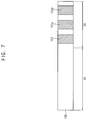
- FIG. 1 is a plan view illustrating a display device according to an embodiment.
- FIG. 2 is a cross-sectional view illustrating the display device in FIG. 1 .
- FIG. 3 is an enlarged partial cross-sectional view illustrating the display device in FIG. 2 .
- FIG. 4 is a plan view illustrating a sealing member and conductive members included in the display device in FIG. 3 .
- FIGS. 5 to 14 are cross-sectional views illustrating a method of manufacturing a display device, according to an embodiment.
- FIG. 15 is a cross-sectional view illustrating a display device according to another embodiment.
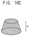
- FIGS. 16A to 16C are schematic diagrams illustrating a bump formed in the display device in FIG. 15 , according to various embodiments.
- FIGS. 17 to 19 are cross-sectional views illustrating a method of manufacturing a display device, according to another embodiment.
- FIG. 20 is a cross-sectional view illustrating a display device according to another embodiment.
- FIGS. 21 to 24 are cross-sectional views illustrating a method of manufacturing a display device, according to another embodiment.
- FIG. 1 is a plan view illustrating a display device according to an embodiment.
- a display device may include a display region 10 and a sealing region 20 .
- An image may be displayed at the display region 10 .
- a plurality of pixels may be disposed in the display region 10 , and light emitted from the pixels may form the image.
- the sealing region 20 may be located adjacent to the display region 10 . In an embodiment, the sealing region 20 may be disposed outside the display region 10 while surrounding a perimeter of the display region 10 .
- the sealing region 20 may be a non-display region on which an image is not displayed.
- FIG. 1 illustrates an embodiment in which the display device has a quadrangular shape in a plan view; however, a planar shape of the display device is not limited thereto.
- the display device may have any of other planar shapes, such as a star shape, a heart shape, a triangle shape, or the like.
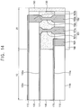
- FIG. 2 is a cross-sectional view illustrating the display device in FIG. 1 ; and FIG. 3 is an enlarged partial cross-sectional view illustrating the display device in FIG. 2 .
- a display device may include a first substrate 110 , a second substrate 120 , a sealing member 130 , a display member 140 , a driving circuit 160 , and conductive members 151 , 152 , and 153 .
- the first substrate 110 and the second substrate 120 may be opposite to each other.
- the first substrate 110 may have a first surface 110 a facing the second substrate 120 and a second surface 110 b opposite to the first surface 110 a .
- the first surface 110 a of the first substrate 110 may be an upper surface
- the second surface 110 b of the first substrate 110 may be a lower surface.
- the second substrate 120 may have a first surface 120 a facing the first substrate 110 and a second surface 120 b opposite to the first surface 120 a .
- the first surface 120 a of the second substrate 120 may be a lower surface
- the second surface 120 b of the second substrate 120 may be an upper surface.
- the first substrate 110 may include a thin film transistor and a pixel electrode
- the second substrate 120 may include a common electrode.
- the display member 140 may be disposed in the display region 10 between the first substrate 110 and the second substrate 120 .
- the display member 140 may include a liquid crystal layer.
- the sealing member 130 may be disposed in the sealing region 20 between the first substrate 110 and the second substrate 120 .
- the sealing member 130 may contact the first surface 110 a of the first substrate 110 and the first surface 120 a of the second substrate 120 so as to encapsulate the display member 140 .
- the display device may further include an external sealing member 190 .
- the external sealing member 190 may contact a side surface between the first surface 110 a and the second surface 110 b of the first substrate 110 and a side surface between the first surface 120 a and the second surface 120 b of the second substrate 120 so as to encapsulate the side surface of the first substrate 110 and the side surface of the second substrate 120 .
- Wirings 171 , 172 , and 173 may be formed on the first substrate 110 and the second substrate 120 .
- a first wiring 171 may be formed on the first surface 120 a of the second substrate 120 .
- the first wiring 171 may extend from the display region 10 to the sealing region 20 .
- the first wiring 171 may be a common voltage line.
- the first wiring 171 may be connected to the common electrode, and may transmit a common voltage.
- a second wiring 172 may be formed on the second surface 120 b of the second substrate 120 .
- the second wiring 172 may extend from the display region 10 to the sealing region 20 .
- the second wiring 172 may be a touch line.
- the second wiring 172 may be connected to a touch sensing member, and may transmit a driving signal or a sensing signal.
- the second wiring 172 may be connected to a fingerprint recognition member.
- a third wiring 173 may be formed on the first surface 110 a of the first substrate 110 .
- the third wiring 173 may extend from the display region 10 to the sealing region 20 .
- the third wiring 173 may be a gate line or a data line.
- the third wiring 173 may be connected to the thin film transistor, and may transmit a gate signal or a data voltage.
- the driving circuit 160 may be electrically connected to the first wiring 171 , the second wiring 172 , and the third wiring 173 .
- the driving circuit 160 may be disposed on the second surface 110 b of the first substrate 110 . Accordingly, an increase of a width of a bezel of the display device may be prevented or substantially prevented.
- the driving circuit 160 may generate the common voltage, the driving signal, the sensing signal, the gate signal, and the data voltage, and may transmit those to the wirings 171 , 172 , and 173 .
- the conductive members 151 , 152 , and 153 may connect the driving circuit 160 to the wirings 171 , 172 , and 173 .
- the conductive members 151 , 152 , and 153 may include a first conductive member 151 , a second conductive member 152 , and a third conductive member 153 .
- the first conductive member 151 may connect the driving circuit 160 to the first wiring 171 .
- the first conductive member 151 may overlap the sealing member 130 , and may pass through the first substrate 110 and the sealing member 130 .
- the first conductive member 151 may contact the first wiring 171 .
- the first conductive member 151 may transmit the common voltage transmitted from the driving circuit 160 to the first wiring 171 .
- the display device may include a plurality of first conductive members 151 .
- the first conductive member 151 may include a first lower conductive member 151 a passing through the first substrate 110 and a first middle conductive member 151 c passing through the sealing member 130 .
- a width of the first lower conductive member 151 a may be different from a width of the first middle conductive member 151 c .
- the width of the first middle conductive member 151 c may be less than the width of the first lower conductive member 151 a.
- the second conductive member 152 may connect the driving circuit 160 to the second wiring 172 .
- the second conductive member 152 may overlap the sealing member 130 , and may pass through the first substrate 110 , the sealing member 130 , and the second substrate 120 .
- the second conductive member 152 may contact the second wiring 172 .
- the second conductive member 152 may transmit the driving signal or the sensing signal transmitted from the driving circuit 160 to the second wiring 172 .
- the display device may include a plurality of second conductive members 152 .
- the second conductive member 152 may include a second lower conductive member 152 a passing through the first substrate 110 , an upper conductive member 152 b passing through the second substrate 120 , and a second middle conductive member 152 c passing through the sealing member 130 .
- a width of the second lower conductive member 152 a may be substantially the same as a width of the upper conductive member 152 b
- the width of the second lower conductive member 152 a may be different from a width of the second middle conductive member 152 c .
- the width of the second middle conductive member 152 c may be less than the width of the second lower conductive member 152 a.
- the third conductive member 153 may connect the driving circuit 160 to the third wiring 173 .
- the third conductive member 153 may overlap the sealing member 130 , and may pass through the first substrate 110 .
- the third conductive member 153 may contact the third wiring 173 .
- the third conductive member 153 may transmit the gate signal or the data voltage transmitted from the driving circuit 160 to the third wiring 173 .
- the display device according to an embodiment may include a plurality of third conductive members 153 .
- the driving circuit 160 may directly contact the conductive members 151 , 152 , and 153 .
- the display device may further include a printed circuit board.
- the driving circuit 160 may be disposed on the printed circuit board, and may be connected to the conductive members 151 , 152 , and 153 through the printed circuit board.
- the display device may further include a backlight unit.
- the backlight unit may be provided as a direct type backlight unit.
- the backlight unit may be disposed on the second surface 110 b of the first substrate 110 , and may emit light to the first substrate 110 . Accordingly, an increase of a width of a bezel of the display device may be prevented or substantially prevented.
- FIG. 4 is a plan view illustrating a sealing member and conductive members included in the display device in FIG. 3 .
- the sealing member 130 may be disposed in the sealing region 20 , and the conductive members 151 , 152 , and 153 may overlap the sealing member 130 .
- a width W of the sealing member 130 may be less than about 50 ⁇ m.
- the sealing member 130 may be located in a bezel of the display device, and in order to narrowly form the bezel of the display device, the smaller width W of the sealing member 130 may be more advantageous.
- each of the conductive members 151 , 152 , and 153 may have a circular shape in a plan view.
- a diameter of each of the conductive members 151 , 152 , and 153 may be less than about 30 ⁇ m, and, in an embodiment, less than about 10 ⁇ m.
- a planar shape of each of the conductive members 151 , 152 , and 153 is not limited thereto, and each of the conductive members 151 , 152 , and 153 may have any of various polygonal planar shapes.
- the conductive members 151 , 152 , and 153 may be alternately disposed with respect to each other.
- the first conductive member 151 and the second conductive member 152 may be alternately disposed with respect to each other in a width direction parallel to the width W of the sealing member 130
- the first conductive member 151 and the third conductive member 153 may be alternately disposed with respect to each other in the width direction.
- the width W of the sealing member 130 is relatively small, a relatively large number of the conductive members 151 , 152 , and 153 may be disposed while overlapping the sealing member 130 .
- the present invention is not limited thereto, and the conductive members 151 , 152 , and 153 may be disposed aligned to each other in the width direction.
- the conductive member 151 , 152 , and 153 connecting the driving circuit 160 and the wirings 171 , 172 , and 173 may overlap the sealing member 130 and, therefore, the display device may have a narrow bezel.
- FIGS. 5 to 14 are cross-sectional views illustrating a method of manufacturing a display device, according to an embodiment.
- a method of manufacturing a display device may include forming a lower conductive member in a first substrate in a sealing region of the display device, forming a wiring on a second substrate, forming a middle conductive member in the sealing region between the first substrate and the second substrate, and forming a sealing member surrounding the middle conductive member.
- the lower conductive members 151 a and 152 a may be formed in the sealing region 20 of the first substrate 110 .
- the first lower conductive member 151 a , the second lower conductive member 152 a , and the third conductive member 153 may be formed in the sealing region 20 of the first substrate 110 .
- the first substrate 110 including an insulation material, such as glass, plastic, etc. may be prepared.
- a thickness of the first substrate 110 may be about 500 ⁇ m.
- a first through hole 111 , a second through hole 112 , and a third through hole 113 may be formed in the sealing region 20 of the first substrate 110 .
- a laser FL may be irradiated at the sealing region 20 of the first substrate 110 .
- the through holes 111 , 112 , and 113 may be formed by a femtosecond laser.
- the through holes 111 , 112 , and 113 having a small diameter may be formed by using the femtosecond laser.
- a diameter of each of the through holes 111 , 112 , and 113 may be less than about 30 ⁇ m, and, in an embodiment, less than about 10 ⁇ m. In an embodiment, a distance between adjacent through holes 111 , 112 , and 113 may be less than about 100 ⁇ m. For example, a distance between the first through hole 111 and the second through hole 112 adjacent to each other and a distance between the first through hole 111 and the third through hole 113 adjacent to each other may be less than about 100 ⁇ m.
- the through holes 111 , 112 , and 113 may be filled with a conductive material.
- the through holes 111 , 112 , and 113 may be filled with silver (Ag).
- the through holes 111 , 112 , and 113 may be filled by using Ag paste.
- the first lower conductive member 151 a , the second lower conductive member 152 a , and the third conductive member 153 may be formed in the first through hole 111 , the second through hole 112 , and the third through hole 113 , respectively.
- the first lower conductive member 151 a and the second lower conductive member 152 a may be portions of the first conductive member 151 and the second conductive member 152 illustrated in FIG. 3 , respectively.
- the upper conductive member 152 b may be formed in a region of the second substrate 120 corresponding to the sealing region 20 .
- the second substrate 120 including an insulation material, such as glass, plastic, etc. may be prepared.
- a thickness of the second substrate 120 may be about 500 ⁇ m.
- a fourth through hole 122 may be formed in a region of the second substrate 120 corresponding to the sealing region 20 .
- a laser FL may be irradiated at the region of the second substrate 120 corresponding to the sealing region 20 .
- the fourth through hole 122 may be formed by a femtosecond laser.
- the fourth through hole 122 having a small diameter may be formed by using the femtosecond laser.
- a diameter of the fourth through hole 122 may be less than about 30 ⁇ m, and, in an embodiment, less than about 10 ⁇ m.
- the fourth through hole 122 may be filled with a conductive material.
- the fourth through hole 122 may be filled with silver (Ag).
- the fourth through hole 122 may be filled by using Ag paste.
- the upper conductive member 152 b may be formed in the fourth through hole 122 .
- the upper conductive member 152 b may be a portion of the second conductive member 152 illustrated in FIG. 3 .
- the wirings 171 , 172 , and 173 may be formed on the second substrate 120 and the first substrate 110 , and the second substrate 120 may be disposed opposite to the first substrate 110 . Further, a first preliminary sealing member 131 may be formed in the sealing region 20 between the first substrate 110 and the second substrate 120 , and the display member 140 may be formed in the display region 10 between the first substrate 110 and the second substrate 120 .
- the wirings 171 , 172 , and 173 may be formed on the first substrate 110 and the second substrate 120 .
- the first wiring 171 may be formed on the first surface 120 a of the second substrate 120 facing the first substrate 110
- the second wiring 172 may be formed on the second surface 120 b of the second substrate 120 opposite to the first surface 120 a
- the third wiring 173 may be formed on the first surface 110 a of the first substrate 110 facing the second substrate 120 .
- the first wiring 171 , the second wiring 172 , and the third wiring 173 may extend from the display region 10 to the sealing region 20 .
- the first preliminary sealing member 131 may be formed in the sealing region 20 between the first substrate 110 and the second substrate 120 .
- the first preliminary sealing member 131 may be a portion of the sealing member 130 illustrated in FIG. 3 .
- the first preliminary sealing member 131 may be formed of an organic material, such as polyimide (PI).
- the first preliminary sealing member 131 may cover the third conductive member 153 , and may expose at least a portion of the first lower conductive member 151 a and at least a portion of an end of the first wiring 171 .
- the display member 140 may be formed in the display region 10 between the first substrate 110 and the second substrate 120 .
- the display member 140 may be formed after the formation of the first preliminary sealing member 131 .
- a liquid crystal may be injected in the display region 10 between the first substrate 110 and the second substrate 120 .
- the display member 140 may be formed after a completion of forming the sealing member 130 .
- bumps may be formed on the first substrate 110 and the second substrate 120 .
- bumps may be formed on the first lower conductive member 151 a and the second lower conductive member 152 a on the first surface 110 a of the first substrate 110
- bumps may be formed on the end of the first wiring 171 and the upper conductive member 152 b on the first surface 120 a of the second substrate 120 .
- the bumps may not be formed.
- the middle conductive members 151 c and 152 c respectively connecting the lower conductive members 151 a and 152 a and the wirings 171 and 172 may be formed in the sealing region 20 between the first substrate 110 and the second substrate 120 .
- the first middle conductive member 151 c connecting the first lower conductive member 151 a and the first wiring 171 and the second middle conductive member 152 c connecting the second lower conductive member 152 a and the second wiring 172 while being in contact with the upper conductive member 152 b may be formed.
- a first conductive line connecting the first lower conductive member 151 a and the first wiring 171 may be formed.
- the first conductive line may be in contact with the bump formed on the first lower conductive member 151 a and the bump formed on the end of the first wiring 171 .
- the first middle conductive member 151 c may include the first conductive line and the bumps disposed at opposite ends thereof.
- the first conductive line may be formed by an inkjet method, a nano-wire filling method, or the like. According to the formation of the first middle conductive member 151 c , the first conductive member 151 including the first lower conductive member 151 a and the first middle conductive member 151 c may be formed.
- a second preliminary sealing member 132 may be formed in the sealing region 20 between the first substrate 110 and the second substrate 120 , and a second conductive line connecting the second lower conductive member 152 a and the upper conductive member 152 b may be formed.
- the second preliminary sealing member 132 may be a portion of the sealing member 130 .
- the second preliminary sealing member 132 may be formed of an organic material, such as polyimide (PI).
- PI polyimide
- the second conductive line may be in contact with the bump formed on the second lower conductive member 152 a and the bump formed on the upper conductive member 152 b .
- the second middle conductive member 152 c may include the second conductive line and the bumps disposed at opposite ends thereof.
- the second conductive line may be formed by an inkjet method, a nano-wire filling method, or the like. According to the formation of the second middle conductive member 152 c , the second conductive member 152 including the second lower conductive member 152 a , the upper conductive member 152 b , and the second middle conductive member 152 c may be formed.
- the sealing member 130 may be formed in the sealing region 20 between the first substrate 110 and the second substrate 120 , and the external sealing member 190 encapsulating side surfaces of the first substrate 110 and the second substrate 120 may be formed. Further, the driving circuit 160 connected to the first conductive member 151 , the second conductive member 152 , and the third conductive member 153 may be disposed.
- the external sealing member 190 may be formed of a material substantially the same as or different from that of the sealing member 130 .
- the external sealing member 190 may be formed of an inorganic material, such as frit.
- the driving circuit 160 may be disposed on the second surface 110 b of the first substrate 110 .
- the relatively small through holes may be formed in the relatively narrow sealing region 20 by the femtosecond laser, and the conductive members 151 , 152 , and 153 may be formed in the through holes. Accordingly, the display device having a relatively narrow bezel may be formed.
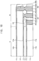
- FIG. 15 a display device according another embodiment will be described with reference to FIG. 15 and FIGS. 16A to 16C .
- FIG. 15 is a cross-sectional view illustrating a display device according to another embodiment.
- a display device may include the first substrate 110 , the second substrate 120 , the sealing member 130 , the display member 140 , the driving circuit 160 , and conductive members 251 , 252 , and 253 .
- a first conductive member 251 may include a first lower conductive member 251 a passing through the first substrate 110 and a first middle conductive member ( 251 d + 251 e ) passing through the sealing member 130 .
- the first middle conductive member ( 251 d + 251 e ) may include a first lower bump 251 d being in contact with the first lower conductive member 251 a and a first upper bump 251 e being in contact with the end of the first wiring 171 .
- a second conductive member 252 may include a second lower conductive member 252 a passing through the first substrate 110 , an upper conductive member 252 b passing through the second substrate 120 , and a second middle conductive member ( 252 d + 252 e ) passing through the sealing member 130 .
- the second middle conductive member ( 252 d + 252 e ) may include a second lower bump 252 d being in contact with the second lower conductive member 252 a and a second upper bump 252 e being in contact with the upper conductive member 252 b.
- FIGS. 16A to 16C are schematic diagrams illustrating a bump formed in the display device in FIG. 15 , according to various embodiments.
- each of the bumps 251 d , 251 e , 252 d , and 252 e may have any of various shapes, such as a hemisphere shape, like shown in FIG. 16A , a circular cylinder shape, like shown in FIG. 16B , a circular truncated cone shape, like shown in FIG. 16C , or the like.
- a height H of each of the bumps 251 d , 251 e , 252 d , and 252 e may be in a range from about 1 ⁇ m to about 2 ⁇ m.
- FIG. 15 a method of manufacturing a display device such as the display device illustrated in FIG. 15 will be described in further detail with reference to FIGS. 17 to 19 .
- FIGS. 17 to 19 are cross-sectional views illustrating a method of manufacturing a display device, according to another embodiment.
- a method of manufacturing a display device may include forming a lower conductive member in a first substrate in a sealing region of the display device, forming a wiring on a second substrate, forming a middle conductive member in the sealing region between the first substrate and the second substrate, and forming a sealing member surrounding the middle conductive member.
- the second substrate 120 may be disposed opposite to the first substrate 110 , and the bumps 251 d , 251 e , 252 d , and 252 e may be formed on the first substrate 110 and the second substrate 120 .
- a preliminary sealing member 133 may be formed in the sealing region 20 between the first substrate 110 and the second substrate 120 .
- the preliminary sealing member 133 may be a portion of the sealing member 130 illustrated in FIG. 15 .
- the display member 140 may be formed in the display region 10 between the first substrate 110 and the second substrate 120 .
- the first lower bump 251 d and the second lower bump 252 d may be formed on the first lower conductive member 251 a and the second lower conductive member 252 a on the first surface 110 a of the first substrate 110 , respectively.
- the first upper bump 251 e and the second upper bump 252 e may be formed on the end of the first wiring 171 and the upper conductive member 252 b on the first surface 120 a of the second substrate 120 , respectively.
- each of the bumps 251 d , 251 e , 252 d , and 252 e may be formed of metal having flexibility, such as silver (Ag).
- each of the bumps 251 d , 251 e , 252 d , and 252 e may be formed to have a thickness between about 1 ⁇ m to about 2 ⁇ m.
- the middle conductive members ( 251 d + 251 e ) and ( 252 d + 252 e ) respectively connecting the lower conductive members 251 a and 252 a and the wirings 171 and 172 may be formed in the sealing region 20 between the first substrate 110 and the second substrate 120 .
- the second middle conductive member ( 252 d + 252 e ) connecting the second lower conductive member 252 a and the second wiring 172 while being in contact with the upper conductive member 252 b may be formed.
- the first substrate 110 and the second substrate 120 may be combined such that the first lower bump 251 d and the second lower bump 252 d are in contact with the first upper bump 251 e and the second upper bump 252 e , respectively.
- the first conductive member 251 including the first lower conductive member 251 a , the first lower bump 251 d , and the first upper bump 251 e ; and the second conductive member 252 including the second lower conductive member 252 a , the upper conductive member 252 b , the second lower bump 252 d , and the second upper bump 252 e may be formed.
- a thickness of the display member 140 may be about 2 ⁇ m, and each of the bumps 251 d , 251 e , 252 d , and 252 e may be formed to have a thickness between about 1 ⁇ m to about 2 ⁇ m. Accordingly, the first conductive member 251 and the second conductive member 252 may be formed without influencing the display member 140 .
- the sealing member 130 may be formed in the sealing region 20 between the first substrate 110 and the second substrate 120 , and the external sealing member 190 encapsulating side surfaces of the first substrate 110 and the second substrate 120 may be formed. Further, the driving circuit 160 connected to the first conductive member 251 , the second conductive member 252 , and the third conductive member 253 may be disposed.
- FIG. 20 is a cross-sectional view illustrating a display device according to another embodiment.
- a display device may include the first substrate 110 , the second substrate 120 , the sealing member 130 , the display member 140 , the driving circuit 160 , and conductive members 351 , 352 , and 353 .
- a first conductive member 351 may include a first lower conductive member 351 a passing through the first substrate 110 and a first middle conductive member 351 f passing through the sealing member 130 .
- a width of the first middle conductive member 351 f may be substantially the same as a width of the first lower conductive member 351 a.
- a second conductive member 352 may include a second lower conductive member 352 a passing through the first substrate 110 , an upper conductive member 352 b passing through the second substrate 120 , and a second middle conductive member 352 f passing through the sealing member 130 .
- a width of the second lower conductive member 352 a , a width of the upper conductive member 352 b , and a width of the second middle conductive member 352 f may be substantially the same.
- FIG. 20 a method of manufacturing a display device such as the display device illustrated in FIG. 20 will be described in further detail with reference to FIGS. 21 to 24 .
- FIGS. 21 to 24 are cross-sectional views illustrating a method of manufacturing a display device, according to another embodiment.
- a method of manufacturing a display device may include forming a lower conductive member in a first substrate in a sealing region of the display device, forming a wiring on a second substrate, forming a middle conductive member in the sealing region between the first substrate and the second substrate, and forming a sealing member surrounding the middle conductive member.
- the second substrate 120 may be disposed opposite to the first substrate 110 , a preliminary sealing member 134 may be formed in the sealing region 20 between the first substrate 110 and the second substrate 120 , and a conductive structure 380 being in contact with the first lower conductive member 351 a , the second lower conductive member 352 a , the end of the first wiring 171 , and the upper conductive member 352 b may be formed in the sealing region 20 between the first substrate 110 and the second substrate 120 .
- the preliminary sealing member 134 may be a portion of the sealing member 130 illustrated in FIG. 20 .
- the conductive structure 380 may be formed of a conductive material.
- the conductive structure 380 may be formed of silver (Ag).
- the conductive structure 380 may be etched to form the first middle conductive member 351 f and the second middle conductive member 352 f.
- the conductive structure 380 may be etched by irradiating a laser FL.
- the laser FL may be irradiated from a side portion of the display device to etch the conductive structure 380 , as illustrated in FIG. 22 .
- the laser FL may be irradiated from an upper portion or a lower portion of the display device to etch the conductive structure 380 , as illustrated in FIG. 23 .
- the first substrate 110 or the second substrate 120 may include a material transmitting the laser FL.
- the sealing member 130 may be formed in the sealing region 20 between the first substrate 110 and the second substrate 120 , and the external sealing member 190 encapsulating the side surfaces of the first substrate 110 and the second substrate 120 may be formed. Further, the driving circuit 160 connected to the first conductive member 351 , the second conductive member 352 , and the third conductive member 353 may be disposed.
- the display device may be applied to a display device included in a computer, a notebook, a mobile phone, a smartphone, a smart pad, a PMP, a PDA, an MP3 player, or the like.
Landscapes
- Physics & Mathematics (AREA)
- Nonlinear Science (AREA)
- General Physics & Mathematics (AREA)
- Chemical & Material Sciences (AREA)
- Crystallography & Structural Chemistry (AREA)
- Optics & Photonics (AREA)
- Mathematical Physics (AREA)
- Engineering & Computer Science (AREA)
- Microelectronics & Electronic Packaging (AREA)
- Computer Hardware Design (AREA)
- Theoretical Computer Science (AREA)
- Spectroscopy & Molecular Physics (AREA)
- Devices For Indicating Variable Information By Combining Individual Elements (AREA)
- Liquid Crystal (AREA)
Abstract
Description
Claims (20)
Applications Claiming Priority (2)
| Application Number | Priority Date | Filing Date | Title |
|---|---|---|---|
| KR1020170143651A KR20190049972A (en) | 2017-10-31 | 2017-10-31 | Display device and method of manufacturing the same |
| KR10-2017-0143651 | 2017-10-31 |
Publications (2)
| Publication Number | Publication Date |
|---|---|
| US20190129266A1 US20190129266A1 (en) | 2019-05-02 |
| US10698280B2 true US10698280B2 (en) | 2020-06-30 |
Family
ID=66243744
Family Applications (1)
| Application Number | Title | Priority Date | Filing Date |
|---|---|---|---|
| US15/994,908 Expired - Fee Related US10698280B2 (en) | 2017-10-31 | 2018-05-31 | Display device and method of manufacturing the same |
Country Status (3)
| Country | Link |
|---|---|
| US (1) | US10698280B2 (en) |
| KR (1) | KR20190049972A (en) |
| CN (1) | CN109727545A (en) |
Cited By (1)
| Publication number | Priority date | Publication date | Assignee | Title |
|---|---|---|---|---|
| US11772191B2 (en) | 2019-10-24 | 2023-10-03 | Samsung Display Co., Ltd. | Substrate processing apparatus and method |
Families Citing this family (4)
| Publication number | Priority date | Publication date | Assignee | Title |
|---|---|---|---|---|
| KR102783662B1 (en) * | 2019-06-20 | 2025-03-20 | 삼성디스플레이 주식회사 | Display device |
| CN110782799B (en) * | 2019-11-21 | 2022-01-04 | 昆山国显光电有限公司 | Display panel and preparation method thereof |
| CN118884746A (en) * | 2024-07-29 | 2024-11-01 | 惠科股份有限公司 | Display panel and display device |
| CN118981131B (en) * | 2024-10-22 | 2025-01-17 | 惠科股份有限公司 | Liquid crystal display panel and electronic equipment |
Citations (11)
| Publication number | Priority date | Publication date | Assignee | Title |
|---|---|---|---|---|
| US6618111B1 (en) | 1999-10-21 | 2003-09-09 | Sharp Kabushiki Kaisha | Liquid crystal display device |
| JP2005274632A (en) | 2004-03-23 | 2005-10-06 | Sharp Corp | Liquid crystal module and liquid crystal display device including the same |
| JP2008077029A (en) | 2006-09-22 | 2008-04-03 | Samsung Sdi Co Ltd | Flat panel display device and portable display device |
| US20120033162A1 (en) * | 2010-08-09 | 2012-02-09 | Samsung Mobile Display Co., Ltd. | Liquid crystal display device |
| US20130016065A1 (en) * | 2011-07-13 | 2013-01-17 | Synaptics Incorporated | Trace shielding for input devices |
| KR20130109350A (en) | 2012-03-27 | 2013-10-08 | 엘지디스플레이 주식회사 | Display device and manufacturing for method thereof |
| US8687139B2 (en) | 2008-12-15 | 2014-04-01 | Lg Display Co., Ltd. | Liquid crystal display device having reduced static electricity |
| US20150002500A1 (en) * | 2013-07-01 | 2015-01-01 | Samsung Display Co., Ltd. | Liquid crystal display |
| KR20150145827A (en) | 2014-06-19 | 2015-12-31 | 삼성디스플레이 주식회사 | Display module and multi desplay device comprising the same |
| US9582031B2 (en) | 2010-05-19 | 2017-02-28 | Lg Electronics Inc. | Mobile device |
| US20170160866A1 (en) * | 2015-12-08 | 2017-06-08 | Innolux Corporation | Touch display device |
Family Cites Families (9)
| Publication number | Priority date | Publication date | Assignee | Title |
|---|---|---|---|---|
| TW479213B (en) * | 1999-07-22 | 2002-03-11 | Seiko Epson Corp | Liquid crystal apparatus, its manufacturing method, and electronic machine |
| JP2005215358A (en) * | 2004-01-30 | 2005-08-11 | Citizen Watch Co Ltd | Liquid crystal optical element and method for manufacturing the same |
| JP2007121687A (en) * | 2005-10-28 | 2007-05-17 | Epson Imaging Devices Corp | Liquid crystal display device |
| KR20110106084A (en) * | 2010-03-22 | 2011-09-28 | 삼성전자주식회사 | Field emission type surface light source device and image display device employing the same |
| CN103984145B (en) * | 2013-12-09 | 2017-07-07 | 上海天马微电子有限公司 | Embedded touch screen color film substrate and manufacturing method thereof |
| CN103698948B (en) * | 2013-12-20 | 2016-07-06 | 京东方科技集团股份有限公司 | A kind of liquid crystal panel and liquid crystal display |
| KR102124906B1 (en) * | 2013-12-26 | 2020-07-07 | 엘지디스플레이 주식회사 | Organic electro luminescent device having touch screen and method of fabricationg the same |
| CN104570520B (en) * | 2014-12-31 | 2017-12-26 | 上海天马微电子有限公司 | Liquid crystal lens |
| JP2017111297A (en) * | 2015-12-16 | 2017-06-22 | 株式会社ジャパンディスプレイ | Display device |
-
2017
- 2017-10-31 KR KR1020170143651A patent/KR20190049972A/en not_active Ceased
-
2018
- 2018-05-31 US US15/994,908 patent/US10698280B2/en not_active Expired - Fee Related
- 2018-09-14 CN CN201811072856.4A patent/CN109727545A/en active Pending
Patent Citations (11)
| Publication number | Priority date | Publication date | Assignee | Title |
|---|---|---|---|---|
| US6618111B1 (en) | 1999-10-21 | 2003-09-09 | Sharp Kabushiki Kaisha | Liquid crystal display device |
| JP2005274632A (en) | 2004-03-23 | 2005-10-06 | Sharp Corp | Liquid crystal module and liquid crystal display device including the same |
| JP2008077029A (en) | 2006-09-22 | 2008-04-03 | Samsung Sdi Co Ltd | Flat panel display device and portable display device |
| US8687139B2 (en) | 2008-12-15 | 2014-04-01 | Lg Display Co., Ltd. | Liquid crystal display device having reduced static electricity |
| US9582031B2 (en) | 2010-05-19 | 2017-02-28 | Lg Electronics Inc. | Mobile device |
| US20120033162A1 (en) * | 2010-08-09 | 2012-02-09 | Samsung Mobile Display Co., Ltd. | Liquid crystal display device |
| US20130016065A1 (en) * | 2011-07-13 | 2013-01-17 | Synaptics Incorporated | Trace shielding for input devices |
| KR20130109350A (en) | 2012-03-27 | 2013-10-08 | 엘지디스플레이 주식회사 | Display device and manufacturing for method thereof |
| US20150002500A1 (en) * | 2013-07-01 | 2015-01-01 | Samsung Display Co., Ltd. | Liquid crystal display |
| KR20150145827A (en) | 2014-06-19 | 2015-12-31 | 삼성디스플레이 주식회사 | Display module and multi desplay device comprising the same |
| US20170160866A1 (en) * | 2015-12-08 | 2017-06-08 | Innolux Corporation | Touch display device |
Cited By (1)
| Publication number | Priority date | Publication date | Assignee | Title |
|---|---|---|---|---|
| US11772191B2 (en) | 2019-10-24 | 2023-10-03 | Samsung Display Co., Ltd. | Substrate processing apparatus and method |
Also Published As
| Publication number | Publication date |
|---|---|
| US20190129266A1 (en) | 2019-05-02 |
| CN109727545A (en) | 2019-05-07 |
| KR20190049972A (en) | 2019-05-10 |
Similar Documents
| Publication | Publication Date | Title |
|---|---|---|
| US10698280B2 (en) | Display device and method of manufacturing the same | |
| KR102783387B1 (en) | Display apparatus and method of manufacturing the same | |
| US11532797B2 (en) | Display apparatus including glass substrates | |
| KR102369089B1 (en) | Flexible display device | |
| US9899428B2 (en) | Display device having terminal electrode including stepped surface | |
| KR102300254B1 (en) | Display device | |
| TWI545632B (en) | Organic light emitting display device and method of manufacturing same | |
| KR102204976B1 (en) | Display apparatus and fabrication method thereof | |
| US9508752B2 (en) | Display device and method of manufacturing the same | |
| KR102654664B1 (en) | Organic light emitting display device | |
| US20170010638A1 (en) | Display device | |
| US12015007B2 (en) | Adhesive member and display device including the same | |
| US10817025B2 (en) | Narrow-bezel display module and display device | |
| KR20190122920A (en) | Display device | |
| KR20250114469A (en) | Display apparatus | |
| KR20250047513A (en) | Display device | |
| KR20250112203A (en) | Sensing unit | |
| WO2020118836A1 (en) | Touch screen and display device | |
| KR102888967B1 (en) | Display apparatus | |
| CN106848086B (en) | Organic Light Emitting Diode and preparation method thereof, display device | |
| KR20240049124A (en) | Thin film transistor, and transistor array substrate | |
| KR20260032802A (en) | Display device and method for fabricating the same | |
| KR20250098054A (en) | Display device and method of manufacturing the same | |
| KR20250045507A (en) | Display device and method of manufacturing the same | |
| KR20220097742A (en) | Display device and method of manufacturing the display device |
Legal Events
| Date | Code | Title | Description |
|---|---|---|---|
| AS | Assignment |
Owner name: SAMSUNG DISPLAY CO., LTD., KOREA, REPUBLIC OF Free format text: ASSIGNMENT OF ASSIGNORS INTEREST;ASSIGNOR:FUKASAWA, TAKAYUKI;REEL/FRAME:045957/0127 Effective date: 20180427 |
|
| FEPP | Fee payment procedure |
Free format text: ENTITY STATUS SET TO UNDISCOUNTED (ORIGINAL EVENT CODE: BIG.); ENTITY STATUS OF PATENT OWNER: LARGE ENTITY |
|
| STPP | Information on status: patent application and granting procedure in general |
Free format text: DOCKETED NEW CASE - READY FOR EXAMINATION |
|
| STPP | Information on status: patent application and granting procedure in general |
Free format text: NON FINAL ACTION MAILED |
|
| STPP | Information on status: patent application and granting procedure in general |
Free format text: NON FINAL ACTION MAILED |
|
| STPP | Information on status: patent application and granting procedure in general |
Free format text: NOTICE OF ALLOWANCE MAILED -- APPLICATION RECEIVED IN OFFICE OF PUBLICATIONS |
|
| STCF | Information on status: patent grant |
Free format text: PATENTED CASE |
|
| FEPP | Fee payment procedure |
Free format text: MAINTENANCE FEE REMINDER MAILED (ORIGINAL EVENT CODE: REM.); ENTITY STATUS OF PATENT OWNER: LARGE ENTITY |
|
| LAPS | Lapse for failure to pay maintenance fees |
Free format text: PATENT EXPIRED FOR FAILURE TO PAY MAINTENANCE FEES (ORIGINAL EVENT CODE: EXP.); ENTITY STATUS OF PATENT OWNER: LARGE ENTITY |
|
| STCH | Information on status: patent discontinuation |
Free format text: PATENT EXPIRED DUE TO NONPAYMENT OF MAINTENANCE FEES UNDER 37 CFR 1.362 |
|
| FP | Lapsed due to failure to pay maintenance fee |
Effective date: 20240630 |