US10698147B2 - Polarizing element - Google Patents
Polarizing element Download PDFInfo
- Publication number
- US10698147B2 US10698147B2 US15/564,503 US201615564503A US10698147B2 US 10698147 B2 US10698147 B2 US 10698147B2 US 201615564503 A US201615564503 A US 201615564503A US 10698147 B2 US10698147 B2 US 10698147B2
- Authority
- US
- United States
- Prior art keywords
- grid
- polarizing element
- inclination
- width
- tips
- Prior art date
- Legal status (The legal status is an assumption and is not a legal conclusion. Google has not performed a legal analysis and makes no representation as to the accuracy of the status listed.)
- Active
Links
- 239000000758 substrate Substances 0.000 claims abstract description 47
- 238000010521 absorption reaction Methods 0.000 claims description 76
- 238000003491 array Methods 0.000 claims 1
- 238000002834 transmittance Methods 0.000 description 49
- 230000005540 biological transmission Effects 0.000 description 43
- 238000004088 simulation Methods 0.000 description 26
- 239000000463 material Substances 0.000 description 20
- 230000000694 effects Effects 0.000 description 15
- 238000005259 measurement Methods 0.000 description 14
- 229910052751 metal Inorganic materials 0.000 description 10
- 239000002184 metal Substances 0.000 description 10
- 230000003287 optical effect Effects 0.000 description 10
- 238000013461 design Methods 0.000 description 9
- VYPSYNLAJGMNEJ-UHFFFAOYSA-N Silicium dioxide Chemical compound O=[Si]=O VYPSYNLAJGMNEJ-UHFFFAOYSA-N 0.000 description 8
- 230000008033 biological extinction Effects 0.000 description 7
- 230000007423 decrease Effects 0.000 description 6
- 230000005684 electric field Effects 0.000 description 6
- 230000006872 improvement Effects 0.000 description 6
- 230000031700 light absorption Effects 0.000 description 6
- 238000000034 method Methods 0.000 description 6
- 239000004065 semiconductor Substances 0.000 description 6
- 230000002238 attenuated effect Effects 0.000 description 4
- 239000000470 constituent Substances 0.000 description 4
- 239000011521 glass Substances 0.000 description 4
- 230000008859 change Effects 0.000 description 3
- 229910052732 germanium Inorganic materials 0.000 description 3
- 239000011347 resin Substances 0.000 description 3
- 229920005989 resin Polymers 0.000 description 3
- 239000011034 rock crystal Substances 0.000 description 3
- 229910052710 silicon Inorganic materials 0.000 description 3
- 239000000126 substance Substances 0.000 description 3
- 229910052719 titanium Inorganic materials 0.000 description 3
- 239000010936 titanium Substances 0.000 description 3
- 229910052721 tungsten Inorganic materials 0.000 description 3
- GWEVSGVZZGPLCZ-UHFFFAOYSA-N Titan oxide Chemical compound O=[Ti]=O GWEVSGVZZGPLCZ-UHFFFAOYSA-N 0.000 description 2
- 229910045601 alloy Inorganic materials 0.000 description 2
- 239000000956 alloy Substances 0.000 description 2
- 229910052782 aluminium Inorganic materials 0.000 description 2
- 229910052804 chromium Inorganic materials 0.000 description 2
- 229910052681 coesite Inorganic materials 0.000 description 2
- 229910052802 copper Inorganic materials 0.000 description 2
- 229910052906 cristobalite Inorganic materials 0.000 description 2
- 239000013078 crystal Substances 0.000 description 2
- 238000009792 diffusion process Methods 0.000 description 2
- 238000005530 etching Methods 0.000 description 2
- 229910052742 iron Inorganic materials 0.000 description 2
- 239000004973 liquid crystal related substance Substances 0.000 description 2
- 229910001635 magnesium fluoride Inorganic materials 0.000 description 2
- 238000004519 manufacturing process Methods 0.000 description 2
- 239000007769 metal material Substances 0.000 description 2
- 150000002739 metals Chemical class 0.000 description 2
- 229910052759 nickel Inorganic materials 0.000 description 2
- 230000008569 process Effects 0.000 description 2
- 239000010980 sapphire Substances 0.000 description 2
- 229910052594 sapphire Inorganic materials 0.000 description 2
- 239000000377 silicon dioxide Substances 0.000 description 2
- 229910052709 silver Inorganic materials 0.000 description 2
- 229910052682 stishovite Inorganic materials 0.000 description 2
- 229910052715 tantalum Inorganic materials 0.000 description 2
- 229910052905 tridymite Inorganic materials 0.000 description 2
- FRWYFWZENXDZMU-UHFFFAOYSA-N 2-iodoquinoline Chemical compound C1=CC=CC2=NC(I)=CC=C21 FRWYFWZENXDZMU-UHFFFAOYSA-N 0.000 description 1
- 229910052582 BN Inorganic materials 0.000 description 1
- 229910016064 BaSi2 Inorganic materials 0.000 description 1
- PZNSFCLAULLKQX-UHFFFAOYSA-N Boron nitride Chemical compound N#B PZNSFCLAULLKQX-UHFFFAOYSA-N 0.000 description 1
- OKTJSMMVPCPJKN-UHFFFAOYSA-N Carbon Chemical compound [C] OKTJSMMVPCPJKN-UHFFFAOYSA-N 0.000 description 1
- 229910021359 Chromium(II) silicide Inorganic materials 0.000 description 1
- 229910018999 CoSi2 Inorganic materials 0.000 description 1
- 229910017623 MgSi2 Inorganic materials 0.000 description 1
- 229910012990 NiSi2 Inorganic materials 0.000 description 1
- -1 SiO2 Chemical class 0.000 description 1
- XUIMIQQOPSSXEZ-UHFFFAOYSA-N Silicon Chemical compound [Si] XUIMIQQOPSSXEZ-UHFFFAOYSA-N 0.000 description 1
- 230000004075 alteration Effects 0.000 description 1
- PNEYBMLMFCGWSK-UHFFFAOYSA-N aluminium oxide Inorganic materials [O-2].[O-2].[O-2].[Al+3].[Al+3] PNEYBMLMFCGWSK-UHFFFAOYSA-N 0.000 description 1
- 230000004888 barrier function Effects 0.000 description 1
- LTPBRCUWZOMYOC-UHFFFAOYSA-N beryllium oxide Inorganic materials O=[Be] LTPBRCUWZOMYOC-UHFFFAOYSA-N 0.000 description 1
- 230000015572 biosynthetic process Effects 0.000 description 1
- 229910000416 bismuth oxide Inorganic materials 0.000 description 1
- 229910052810 boron oxide Inorganic materials 0.000 description 1
- 229910052799 carbon Inorganic materials 0.000 description 1
- 238000004040 coloring Methods 0.000 description 1
- 238000007796 conventional method Methods 0.000 description 1
- 238000001816 cooling Methods 0.000 description 1
- 229910052593 corundum Inorganic materials 0.000 description 1
- 229910001610 cryolite Inorganic materials 0.000 description 1
- 230000006866 deterioration Effects 0.000 description 1
- TYIXMATWDRGMPF-UHFFFAOYSA-N dibismuth;oxygen(2-) Chemical compound [O-2].[O-2].[O-2].[Bi+3].[Bi+3] TYIXMATWDRGMPF-UHFFFAOYSA-N 0.000 description 1
- JKWMSGQKBLHBQQ-UHFFFAOYSA-N diboron trioxide Chemical compound O=BOB=O JKWMSGQKBLHBQQ-UHFFFAOYSA-N 0.000 description 1
- 238000011156 evaluation Methods 0.000 description 1
- GNPVGFCGXDBREM-UHFFFAOYSA-N germanium atom Chemical compound [Ge] GNPVGFCGXDBREM-UHFFFAOYSA-N 0.000 description 1
- ORUIBWPALBXDOA-UHFFFAOYSA-L magnesium fluoride Chemical compound [F-].[F-].[Mg+2] ORUIBWPALBXDOA-UHFFFAOYSA-L 0.000 description 1
- 229910044991 metal oxide Inorganic materials 0.000 description 1
- 150000004706 metal oxides Chemical class 0.000 description 1
- 239000002923 metal particle Substances 0.000 description 1
- 239000000203 mixture Substances 0.000 description 1
- 229910052750 molybdenum Inorganic materials 0.000 description 1
- 229910052758 niobium Inorganic materials 0.000 description 1
- 239000005304 optical glass Substances 0.000 description 1
- 238000005457 optimization Methods 0.000 description 1
- BPUBBGLMJRNUCC-UHFFFAOYSA-N oxygen(2-);tantalum(5+) Chemical compound [O-2].[O-2].[O-2].[O-2].[O-2].[Ta+5].[Ta+5] BPUBBGLMJRNUCC-UHFFFAOYSA-N 0.000 description 1
- 238000000206 photolithography Methods 0.000 description 1
- 230000001681 protective effect Effects 0.000 description 1
- 239000010453 quartz Substances 0.000 description 1
- 230000005855 radiation Effects 0.000 description 1
- 230000009467 reduction Effects 0.000 description 1
- 230000004044 response Effects 0.000 description 1
- 239000005368 silicate glass Substances 0.000 description 1
- 229910021332 silicide Inorganic materials 0.000 description 1
- FVBUAEGBCNSCDD-UHFFFAOYSA-N silicide(4-) Chemical compound [Si-4] FVBUAEGBCNSCDD-UHFFFAOYSA-N 0.000 description 1
- 239000010703 silicon Substances 0.000 description 1
- 239000005361 soda-lime glass Substances 0.000 description 1
- 238000004544 sputter deposition Methods 0.000 description 1
- 238000000992 sputter etching Methods 0.000 description 1
- 229910001936 tantalum oxide Inorganic materials 0.000 description 1
- 229910052714 tellurium Inorganic materials 0.000 description 1
- 229910052718 tin Inorganic materials 0.000 description 1
- 239000004408 titanium dioxide Substances 0.000 description 1
- 238000007740 vapor deposition Methods 0.000 description 1
- 229910001845 yogo sapphire Inorganic materials 0.000 description 1
- XLOMVQKBTHCTTD-UHFFFAOYSA-N zinc oxide Inorganic materials [Zn]=O XLOMVQKBTHCTTD-UHFFFAOYSA-N 0.000 description 1
- 229910006578 β-FeSi2 Inorganic materials 0.000 description 1
Images


Classifications
-
- G—PHYSICS
- G02—OPTICS
- G02B—OPTICAL ELEMENTS, SYSTEMS OR APPARATUS
- G02B5/00—Optical elements other than lenses
- G02B5/30—Polarising elements
- G02B5/3025—Polarisers, i.e. arrangements capable of producing a definite output polarisation state from an unpolarised input state
- G02B5/3058—Polarisers, i.e. arrangements capable of producing a definite output polarisation state from an unpolarised input state comprising electrically conductive elements, e.g. wire grids, conductive particles
-
- G—PHYSICS
- G02—OPTICS
- G02B—OPTICAL ELEMENTS, SYSTEMS OR APPARATUS
- G02B5/00—Optical elements other than lenses
- G02B5/30—Polarising elements
- G02B5/3025—Polarisers, i.e. arrangements capable of producing a definite output polarisation state from an unpolarised input state
- G02B5/3066—Polarisers, i.e. arrangements capable of producing a definite output polarisation state from an unpolarised input state involving the reflection of light at a particular angle of incidence, e.g. Brewster's angle
Definitions
- This disclosure relates to a polarizing element having a wire grid structure.
- a polarizing element is an optical element that absorbs light polarized in one direction and transmits light polarized in a direction perpendicular to this direction.
- liquid-crystal displays are required to include polarizing elements.
- a polarizing element needs to have excellent heat resistance due to being exposed to intense radiation, and is also demanded to have a size on the scale of a few centimeters and a high extinction ratio.
- Wire grid inorganic polarizing elements have been proposed in response to these demands (for example, refer to PTL 1 and 2).
- a wire grid polarizing element has a structure in which many conductive wires (reflection layer) that extend in one direction are arranged on a substrate at a narrower pitch (tens of nanometers to hundreds of nanometers) than the operating wavelength band.
- TE waves S-waves
- TM waves P-waves
- Wire grid polarizing elements have excellent heat resistance, can be made with a relatively large size, and have a high extinction ratio, which makes them suitable for LCD projector applications and the like.
- a grid structure layer in which protrusion-like lines are arranged at specific intervals is formed on a transparent substrate.
- the grid structure layer is formed from resin.
- sputter etching is used to process tips of the protrusion-like lines into pointed shapes.
- oblique irradiation with metal particles is performed to form a metal layer around each tip of the grid structure layer made of resin.
- wire grid polarizing element In the case of a wire grid polarizing element described in PTL 2, metal wires are formed on a transparent substrate and then a dielectric layer and an absorption layer are provided thereon. Light polarized parallel to an extension direction of the wires (TE waves (S-waves)) is selectively absorbed by the dielectric layer and the absorption layer.
- TE waves S-waves
- the TM wave (P-wave) transmittance of a polarizing element is preferably as high as possible.
- transmittance can be increased by making the grid width of a polarizing element narrower.
- an objective of this disclosure is to provide a wire grid polarizing element having an improved transmission axis direction light transmission characteristic.
- a polarizing element having a wire grid structure comprising: a transparent substrate; and grid-shaped convexities that are arranged on the transparent substrate at a smaller pitch than a wavelength of operating band light and that extend in a specific direction, wherein the grid-shaped convexities include a reflection layer formed on the transparent substrate and grid tips formed with side surfaces that, when viewed in the specific direction, are inclined in a direction of tip tapering.
- ⁇ represents an angle of inclination of the side surfaces of the grid tips relative to the transparent substrate
- a represents height of the grid tips when viewed in the specific direction
- b represents width of the grid-shaped convexities when viewed in the specific direction
- ⁇ 0 arctan(2a/b).
- ⁇ 5> The polarizing element according to any one of the foregoing ⁇ 2> to ⁇ 4>, wherein the polarizing element is designed for light of a specific wavelength in a visible light region and the angle of inclination ⁇ is selected from a range of angles for which absorption axis direction reflectance of light of the specific wavelength is 10% or less.
- ⁇ 6> The polarizing element according to any one of the foregoing ⁇ 1> to ⁇ 5>, wherein the grid tips include, in order from a side corresponding to the transparent substrate, a reflection layer, a dielectric layer, and an absorption layer.
- FIG. 1 is a cross-sectional view illustrating a polarizing element in which the disclosed techniques are adopted;
- FIG. 2 illustrates parameters expressing the shape of the polarizing element in FIG. 1 ;
- FIG. 3 illustrates the definition of an angle of inclination of a grid tip
- FIG. 4 is a graph illustrating a transmission axis transmittance characteristic of a polarizing element relative to the angle of inclination of grid tips as calculated by a simulation for a case in which the height a and width b of the grid tips have a ratio of 6:9;
- FIG. 5 is a graph illustrating an absorption axis reflectance characteristic of a polarizing element relative to the angle of inclination of grid tips as calculated by a simulation for a case in which the height a and width b of the grid tips have a ratio of 6:9;
- FIG. 6 is a graph illustrating a transmission axis transmittance characteristic of a polarizing element relative to the angle of inclination of grid tips as calculated by a simulation for a case in which the height a and width b of the grid tips have a ratio of 8:11;
- FIG. 7 is a graph illustrating an absorption axis reflectance characteristic of a polarizing element relative to the angle of inclination of grid tips as calculated by a simulation for a case in which the height a and width b of the grid tips have a ratio of 8:11;
- FIG. 8 is a graph illustrating a transmission axis transmittance characteristic of a polarizing element relative to the angle of inclination of grid tips as calculated by a simulation for a case in which the height a and width b of the grid tips have a ratio of 8:9;
- FIG. 9 is a graph illustrating an absorption axis reflectance characteristic of a polarizing element relative to the angle of inclination of grid tips as calculated by a simulation for a case in which the height a and width b of the grid tips have a ratio of 8:9;
- FIG. 10 is a graph illustrating a transmission axis transmittance characteristic of a polarizing element relative to the angle of inclination of grid tips as calculated by a simulation for a case in which the height a and width b of the grid tips have a ratio of 10:9;
- FIG. 11 is a graph illustrating an absorption axis reflectance characteristic of a polarizing element relative to the angle of inclination of grid tips as calculated by a simulation for a case in which the height a and width b of the grid tips have a ratio of 10:9;
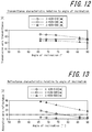
- FIG. 12 is a graph illustrating a transmission axis transmittance characteristic of a polarizing element relative to the angle of inclination of grid tips as calculated by a simulation for a case in which the height a and width b of the grid tips have a ratio of 8:7;
- FIG. 13 is a graph illustrating an absorption axis reflectance characteristic of a polarizing element relative to the angle of inclination of grid tips as calculated by a simulation for a case in which the height a and width b of the grid tips have a ratio of 8:7;
- FIG. 14 is a table indicating ranges for the angle of inclination of grid tips with respect to ratios of the height a and width b of the grid tips;
- FIG. 15 is a graph illustrating actual measurement values and simulation values, in comparison, for a transmission axis transmittance characteristic of a polarizing element relative to the angle of inclination of grid tips for a case in which the height a and width b of the grid tips have a ratio of 8:9;
- FIG. 16 is a graph illustrating actual measurement values of a transmission axis transmittance characteristic for different angles of inclination ⁇ ;
- FIG. 17 is a graph illustrating actual measurement values of an absorption axis transmittance characteristic for different angles of inclination ⁇ ;
- FIG. 18 is a graph illustrating actual measurement values of a transmission axis reflectance characteristic for different angles of inclination ⁇ .
- FIG. 19 is a graph illustrating actual measurement values of an absorption axis reflectance characteristic for different angles of inclination ⁇ .
- FIG. 1 is a schematic cross-sectional view illustrating a polarizing element 1 according to one disclosed embodiment.
- the polarizing element 1 includes a transparent substrate 11 that is transparent with respect to operating band light, and also includes a reflection layer 12 on one surface of the transparent substrate 11 , a dielectric layer 13 formed on the reflection layer 12 , and an absorption layer 14 formed on the dielectric layer 13 that form grid-shaped convexities 10 arranged at a smaller pitch than the wavelength of operating band light.
- the polarizing element 1 has a one-dimensional grid-shaped wire grid structure in which the grid-shaped convexities 10 , having the reflection layer 12 , the dielectric layer 13 , and the absorption layer 14 stacked in this order from the transparent substrate 11 , are arranged at specific intervals on the transparent substrate 11 .
- the grid-shaped convexities 10 are divided into grid bases 15 having side surfaces that extend in parallel in a direction perpendicular to the transparent substrate 11 and grid tips 16 having side surfaces that are inclined in a direction of tapering toward tips of the grid-shaped convexities 10 .
- the boundary between the grid bases 15 and the grid tips 16 is positioned in the reflection layer 12 .
- the grid bases 15 are formed from part of the reflection layer 12 and the grid tips 16 are formed from part of the reflection layer 12 , the dielectric layer 13 , and the absorption layer 14 .
- a direction in which the one-dimensional grid convexities of the grid-shaped convexities 10 extend is referred to as the Y axis direction and a direction along the transparent substrate 11 that is perpendicular to the Y axis direction is referred to as the X axis direction.
- the polarizing element 1 is preferably irradiated with light from a direction that is perpendicular to the X axis direction and the Y axis direction, at a side of the transparent substrate 11 at which the grid-shaped convexities 10 are formed.
- the absorption layer 14 is a material such as a metal or a semiconductor having a non-zero extinction coefficient as an optical constant.
- the absorption layer 14 is a material that displays a light absorption effect.
- the polarizing element 1 may further include a metal film of Ta, W, Nb, Ti, or the like as a diffusion barrier layer between the dielectric layer 13 and the absorption layer 14 to prevent diffusion of the absorption layer 14 .
- the polarizing element 1 may include a deposited protective film of SiO 2 or the like at an uppermost part to improve reliability in terms of moisture resistance or the like, as necessary, so long as any change in optical characteristics does not have an effect in application.
- the polarizing element 1 exploits the four effects of transmission, reflection, interference, and selective light absorption of polarized light waves through optical anisotropy to attenuate polarized light waves having an electric field component parallel to the Y axis direction (TE waves (S-waves)) and transmit polarized light waves having an electric field component parallel to the X axis direction (TM waves (P-waves)).
- TE waves S-waves
- TM waves polarized light waves
- the Y axis direction is an absorption axis direction of the polarizing element 1
- the X axis direction is a transmission axis direction of the polarizing element 1 .
- TM waves that have passed through the absorption layer 14 and the dielectric layer 13 are also transmitted through the reflection layer 12 with a high transmittance.
- TE waves are attenuated due to the light absorption effect of the absorption layer 14 .
- the one-dimensional grid-shaped reflection layer 12 functions as a wire grid and reflects TE waves that have passed through the absorption layer 14 and the dielectric layer 13 .
- a portion of TE waves that are reflected by the reflection layer 12 are absorbed while passing through the absorption layer 14 , and a portion of the TE waves are reflected and return to the reflection layer 12 .
- Light that has passed through the absorption layer 14 is attenuated by interference. In this manner, the polarizing element 1 enables desired polarized light characteristics to be obtained through the selective attenuation of TE waves.
- the transparent substrate 11 is made from a material that is transparent with respect to operating band light and has a refractive index of 1.1 to 2.2.
- the transparent substrate 11 may be made from glass, sapphire, rock crystal, or the like.
- the transparent substrate 11 is formed from an optically active crystal such as rock crystal
- excellent optical characteristics can be obtained by arranging the grid-shaped convexities 10 in a parallel direction or a perpendicular direction relative to the optic axis of the crystal.
- the optic axis is a directional axis for which the difference in refractive indices of an ordinary ray (O) and an extraordinary ray (E) of light travelling in the direction is smallest.
- glass and in particular quartz (refractive index 1.46) or soda lime glass (refractive index 1.51), may be used.
- quartz reffractive index 1.466
- soda lime glass reffractive index 1.51
- a cheap glass material such as silicate glass that is widely available as optical glass may be used so as to lower production costs.
- the reflection layer 12 is an array of thin metal films that extend in a belt shape in the Y axis direction (absorption axis) on the transparent substrate 11 .
- the reflection layer 12 functions as a wire grid polarizer, and among light radiated toward the surface of the transparent substrate 11 on which the wire grid is formed, the reflection layer 12 causes attenuation of polarized light waves (TE waves (S-waves)) having an electric field component in a parallel direction (Y axis direction) to the direction in which the convexities of the wire grid extend, and transmits polarized light waves (TM waves (P-waves)) having an electric field component in a perpendicular direction (X axis direction) to the direction in which the convexities of the wire grid extend.
- TE waves S-waves
- TM waves polarized light waves
- the constituent material of the reflection layer 12 may be a simple substance of a metal such as Al, Ag, Cu, Mo, Cr, Ti, Ni, W, Fe, Si, Ge, or Te, an alloy containing any of these metals, or a semiconductor material.
- a metal such as Al, Ag, Cu, Mo, Cr, Ti, Ni, W, Fe, Si, Ge, or Te
- an alloy containing any of these metals or a semiconductor material.
- metal materials it is possible to use a resin film or an inorganic film other than a metal that is provided with high surface reflectance through coloring or the like.
- the dielectric layer 13 is formed with a film thickness such that the phase of polarized light that has passed through the absorption layer 14 and been reflected by the reflection layer 12 is shifted by a half wavelength relative to polarized light reflected by the absorption layer 14 .
- the film thickness is appropriately set in a range of 1 nm to 500 nm that enables adjustment of the phase of polarized light and enables an increased interference effect.
- the constituent material of the dielectric layer 13 may be a commonly used material, examples of which include metal oxides such as SiO 2 , Al 2 O 3 , beryllium oxide, and bismuth oxide; MgF 2 , cryolite, germanium, titanium dioxide, silicon, magnesium fluoride, boron nitride, boron oxide, tantalum oxide, and carbon, and combinations of any of the preceding examples.
- the refractive index of the dielectric layer 13 is preferably greater than 1.0 and no greater than 2.5. Polarizing element characteristics may be controlled through the material of the dielectric layer 13 since optical characteristics of the reflection layer 12 are also influenced by the refractive index at the periphery of the reflection layer 12 .
- the absorption layer 14 is made from at least one material having a non-zero extinction coefficient as an optical constant and displaying a light absorption effect, such as a metal or a semiconductor.
- the material of the absorption layer 14 is selected in accordance with the wavelength range of used light.
- metal materials that can be used include simple substances of Ta, Al, Ag, Cu, Au, Mo, Cr, Ti, W, Ni, Fe, and Sn, and alloys including any of these metals.
- semiconductor materials that can be used include Si, Ge, Te, ZnO, and silicide materials (for example, ⁇ —FeSi 2 , MgSi 2 , NiSi 2 , BaSi 2 , CrSi 2 , CoSi 2 , and TaSi).
- the polarizing element 1 can be provided with a high extinction ratio with respect to the used visible light region.
- the band gap energy of the semiconductor is required to be no higher than the operating band because the band gap energy influences the absorption effect.
- the band gap energy of the semiconductor is required to be no higher than the operating band because the band gap energy influences the absorption effect.
- the absorption layer 14 can be formed with a high film density by vapor deposition or sputtering. Moreover, the absorption layer 14 may include two or more layers formed from different materials.
- the polarizing element 1 configured as described above can exploit the four effects of transmission, reflection, interference, and selective light absorption of polarized light waves to attenuate polarized light waves having an electric field component in the Y axis direction parallel to the grid of the reflection layer 12 (TE waves (S-waves)) and transmit polarized light waves having an electric field component in the X axis direction perpendicular to the grid (TM waves (P-waves)).
- TE waves are attenuated by the selective light absorption effect of polarized light waves by the absorption layer 14
- TE waves that have passed through the absorption layer 14 and the dielectric layer 13 are reflected by the grid-shaped reflection layer 12 that functions as a wire grid.
- a portion of TE waves reflected by the reflection layer 12 can be reflected when passing through the absorption layer 14 such as to return to the reflection layer 12 , and light that has passed through the absorption layer 14 can be attenuated by interference. In this manner, desired polarized light characteristics can be obtained through the selective attenuation of TE waves.
- FIG. 2 illustrates parameters expressing the shape of the polarizing element 1 illustrated in FIG. 1 .
- “height” refers to a dimension in a direction perpendicular to the surface of the transparent substrate 11 and “width” refers to a dimension in a direction (X axis direction) that perpendicularly intersects the height direction when viewed in a direction (Y axis direction) along the grid-shaped convexities 10 .
- the polarizing element 1 when the polarizing element 1 is viewed in the direction along the grid-shaped convexities 10 (Y axis direction), the repeated intervals between the grid-shaped convexities 10 in the X axis direction are referred to as the “pitch” and the width of each of the grid-shaped convexities 10 in the X axis direction is referred to as the “grid width”.
- the pitch of the polarizing element 1 is smaller than the wavelength of operating band light.
- each of the grid-shaped convexities 10 has a roughly constant width b in the X axis direction at the grid base 15 thereof and has a smaller width than b in the X axis direction at a part at a certain height or higher, close to the tip of the grid-shaped convexity 10 .
- the part of the grid-shaped convexity 10 having a smaller width than b is the grid tip 16 .
- the height of the grid tip 16 is referred to as “a”.
- the angle of inclination of the side surface of the grid tip 16 relative to the surface of the transparent substrate 11 is referred to as “e”. In a case in which the angle of inclination ⁇ of the side surface of the grid tip 16 is constant as illustrated in FIG. 2 , the angle of inclination ⁇ is an angle in a range
- the angle of inclination ⁇ is defined as the angle of inclination of the side surface of the grid tip 16 relative to the transparent substrate 11 at a central position in terms of height of the grid tip 16 (i.e., a position at a height a/2).
- Formation of the grid-shaped convexities 10 of the polarizing element 1 is carried out by, for example, forming films of the reflection layer 12 , the dielectric layer 13 , and the absorption layer 14 on the transparent substrate 11 , and subsequently forming a grid-shaped mask pattern by nanoimprinting, photolithography, or the like. Parts of the reflection layer 12 , the dielectric layer 13 , and the absorption layer 14 at which the mask pattern is not formed are selectively removed by etching to produce a one-dimensional grid extending in a perpendicular direction relative to the transparent substrate 11 . During this process, the grid tips 16 can be provided with inclined side surfaces through optimization of the etching conditions (gas flow rate, gas pressure, power, substrate cooling temperature).
- the transmittance of TM waves is increased through the grid tips 16 each having a shape in which the side surface thereof is inclined in a direction of tapering.
- the reason for this improvement of TM wave transmittance is thought to be that the tapering of the grid tips 16 makes it difficult for scattering of incident light of variable angles to occur.
- the following describes optical characteristics of the polarizing element 1 using simulations and actual measurement results.
- FIGS. 4 to 13 illustrate a transmission axis transmittance characteristic and an absorption axis reflectance characteristic of the polarizing element 1 , relative to the angle of inclination of the grid tips 16 , as calculated by simulations for various ratios of the height (a) and width (b) of the grid tips 16 .
- the term “transmission axis transmittance” refers to the transmittance of transmission axis direction (X axis direction) polarized light (TM waves) that is incident on the polarizing element 1
- the term “absorption axis reflectance” refers to the reflectance of absorption axis direction (Y axis direction) polarized light (TE waves) by the polarizing element 1 .
- These graphs are each for a polarizing element 1 designed such as to be optimized for green band (wavelength 520 nm to 590 nm (specific wavelength)) light.
- FIG. 4 is a graph illustrating the transmission axis transmittance characteristic of the polarizing element 1 relative to the angle of inclination of the grid tip 16 as calculated by a simulation for a case in which the height a and width b of the grid tips 16 have a ratio of 6:9.
- a higher transmission axis transmittance indicates that a higher intensity of desired light is transmitted by the polarizing element 1 .
- FIG. 4 illustrates that a higher intensity of desired light is transmitted by the polarizing element 1 .
- the transmittance increases as the angle of inclination ⁇ becomes inclined from 90° (i.e., moving from right to left in the graph). In particular, there is a significant increase in the transmittance for the blue band.
- FIG. 5 is a graph illustrating the absorption axis reflectance characteristic of the polarizing element 1 relative to the angle of inclination of the grid tips 16 as calculated by a simulation for the case in which the height a and width b of the grid tips 16 have a ratio of 6:9.
- a higher absorption axis reflectance indicates that the polarizing element 1 reflects light polarized in the absorption axis direction (TE waves) with a higher intensity.
- the absorption axis reflectance is preferably low because the reflected light mentioned above reduces the extinction ratio. In many LCD projector applications, there is demand for an absorption axis reflectance of less than 10%. According to FIG.
- the absorption axis reflectance for the green band which is the design wavelength of the polarizing element 1 in this simulation, increases as the angle of inclination ⁇ decreases, and the absorption axis reflectance exceeds 10% when the angle of inclination ⁇ is less than 61°. Therefore, permissible values for the angle of inclination ⁇ in LCD projector applications satisfy 61° ⁇ 90°. This angle is referred to as the “device characteristic angle of inclination”.
- the reason that the absorption axis reflectance increases as the inclination of the grid tips 16 increases is presumed to be that the absorption effect of the dielectric layer 13 and the absorption layer 14 with respect to reflected light (TE waves) decreases due to a decrease in the size of the dielectric layer 13 and the absorption layer 14 in a direction along the transparent substrate 11 as viewed in the direction illustrated in FIGS. 1 and 2 (Y axis direction).
- FIGS. 6 and 7 the transmission axis transmittance characteristic and the absorption axis reflectance characteristic of the polarizing element 1 , relative to the angle of inclination of the grid tips 16 , are illustrated in FIGS. 6 and 7 for a case in which the height a and width b of the grid tips 16 have a ratio of 8:11
- FIGS. 8 and 9 for a case in which the height a and width b of the grid tips 16 have a ratio of 8:9
- FIGS. 10 and 11 for a case in which the height a and width b of the grid tips 16 have a ratio of 10:9
- FIGS. 10 and 11 the transmission axis transmittance characteristic and the absorption axis reflectance characteristic of the polarizing element 1 , relative to the angle of inclination of the grid tips 16 .
- the height a and width b of the grid tips 16 have a ratio of 8:7.
- improvement of the transmission axis transmittance is observed for each of the blue band, the green band, and the red band as the inclination of the side surfaces of the grid tips 16 increases (i.e., as the angle of inclination ⁇ decreases).
- the increase in the transmission axis transmittance for the blue band is greater than for the other bands.
- the absorption axis reflectance of light having a wavelength in the green band exceeds 10% when ⁇ 77° as illustrated in FIG. 13 . Accordingly, the device characteristic angle of inclination in this case is 77° ⁇ 90°.
- the effect of improving the transmission axis transmittance characteristic as the side surfaces of the grid tips 16 are inclined is large as illustrated in FIG. 8 , and the angle of inclination ⁇ can be set as 60° ⁇ 90°.
- FIG. 14 is a table indicating ranges for the angle of inclination ⁇ of the grid tips 16 , relative to the ratio of the height a and width b of the grid tips 16 , based on the results of the simulations illustrated in FIGS. 4 to 13 .
- the transmission axis transmittance of light in each wavelength band increases in the range of the angle of inclination ⁇ for each range included in 2 ⁇ 3 ⁇ a/b ⁇ 8/7, where a/b represents the ratio of the height a and width b of the shape of the grid tips 16 .
- the “device characteristic angle of inclination” refers to an angle of inclination in a range in which the absorption axis reflectance does not exceed 10%.
- the angle of inclination ⁇ preferably satisfies the range for this device characteristic angle of inclination.
- FIG. 15 is a graph illustrating actual measurement results and simulation results, in comparison, for the transmission axis transmittance characteristic of the polarizing element 1 relative to the angle of inclination ⁇ of the side surfaces of the grid tips 16 for a case in which the height a and width b of the grid tips 16 have a ratio of 8:9.
- white marks indicate the same simulation results as illustrated in FIG. 8
- black marks indicate actual measurement values for a case in which the average value of the angle of inclination ⁇ is 77° and a case in which the average value of the angle of inclination ⁇ is 74°.
- the average value of the angle of inclination ⁇ is used because, when an actual polarizing element 1 is produced, there is variation in the angle of inclination of the side surfaces of the grid tips 16 .
- FIG. 15 indicates that even with actual measurement results, the transmission axis transmittance is higher for each of the bands in the case in which the average value of the of the angle of inclination ⁇ is 74° than in the case in which the average value of the angle of inclination ⁇ is 77°.
- the transmission axis transmittance is significantly improved in the blue band. The above demonstrates that the transmission axis transmittance is improved through inclination of the side surfaces of the grid tips 16 (i.e., through reduction of the angle of inclination ⁇ ).
- FIGS. 16 to 19 illustrate actual measurement results for a transmission axis transmittance characteristic, an absorption axis transmittance characteristic, a transmission axis reflectance characteristic, and an absorption axis reflectance characteristic of each of two actual polarizing elements 1 that were produced.
- absorption axis transmittance refers to the transmittance of absorption axis direction (Y axis direction) polarized light (TE waves) that is incident on the polarizing element 1
- transmission axis reflectance refers to the reflectance of transmission axis direction (X axis direction) polarized light (TM waves) that is incident on the polarizing element 1 .
- a solid line indicates a polarizing element for which the angle of inclination ⁇ of side surfaces of grid tips 16 varies in a range of 80° to 84° and a dashed line indicates a polarizing element for which the angle of inclination ⁇ of side surfaces of grid tips 16 varies in a range of 76° to 80°.
- the grid height (a) and width (b) of these two polarizing elements have respective ratios of approximately 2/3 and 8/11, which are close to each other.
- the transmission axis transmittance is substantially constant at approximately 92% to 93% in a visible light region including the blue band for which the wavelength is 430 nm or higher, regardless of wavelength, and transmittance is sufficiently improved. Therefore, the transmittance improvement effect of the disclosed techniques is considered to be large when the angle of inclination ⁇ is 80° or less.
- the absorption axis transmittance illustrated in FIG. 17 which indicates the transmittance of TE waves
- the transmission axis reflectance illustrated in FIG. 18 which indicates the reflectance of TM waves
- the transmission axis reflectance is almost 0 at a wavelength of 450 nm, and increases with increasing deviation from this wavelength.
- the transmission axis reflectance is smaller than the absorption axis reflectance illustrated in FIG. 19 , which indicates the reflectance of TE waves.
- the disclosed polarizing element 1 enables improvement of transmittance of light that is polarized in the transmission axis direction through control of the angle of inclination of the side surfaces of the grid tips 16 in the grid-shaped convexities 10 of the wire grid structure.
- the effect of improving transmittance is particularly large for light at the short wavelength end of the region, inclusive of the blue band.
- the disclosed techniques only the shape of the grid tips 16 is changed, rather than the overall shape of the grid-shaped convexities 10 , and thus the basic structure is the same as in conventional techniques such as described in PTL 2. Therefore, there is no change from conventional polarizing elements in terms of difficulty of production, and reliability can also be maintained.
- the results of simulations and actual measurements are provided for an example in which a polarizing element is designed with the green band as a design wavelength, but the disclosed polarizing element is not limited to being a polarizing element having a wavelength in the green band as a design wavelength.
- the “specific wavelength” can be selected from wavelengths in any visible light region and is not limited to being a wavelength in the green band (520 nm to 590 nm).
- the above-described improvement of transmission axis transmittance achieved by providing the grid tips with a tapered shape can expected whichever wavelength is adopted as the design wavelength. In particular, a large effect can be expected at a short wavelength side of the design wavelength.
- the absorption axis reflectance with respect to the design wavelength can still be reduced by adjusting the film thickness, refractive index, and so forth of the dielectric layer. Therefore, it is possible to ensure a device characteristic angle of inclination range for which the absorption axis reflectance is 10% or less.
- the boundary between the grid bases and the grid tips is positioned in a reflection layer, and although the grid tips include a reflection layer, a dielectric layer, and an absorption layer in the embodiment set forth above, this is not a limitation.
- the grid tips may be formed from an absorption layer and a dielectric layer without including a reflection layer, or may be formed from just an absorption layer.
- inclusion of a reflection layer in the grid tips does enable significant improvement of the transmittance of TM waves passing through the polarizing element 1 .
- the disclosed polarizing element is not limited to LCD projector applications. The disclosed polarizing element can be adopted for various applications as a polarizing element having high transmittance with respect to light polarized in the transmission axis direction.
- the disclosed polarizing element has a high extinction ratio and is, therefore, suitable for adoption as a polarizing element used in an LCD projector.
Landscapes
- Physics & Mathematics (AREA)
- General Physics & Mathematics (AREA)
- Optics & Photonics (AREA)
- Polarising Elements (AREA)
- Liquid Crystal (AREA)
Abstract
Description
Claims (5)
Applications Claiming Priority (3)
| Application Number | Priority Date | Filing Date | Title |
|---|---|---|---|
| JP2015093351A JP5960319B1 (en) | 2015-04-30 | 2015-04-30 | Polarizing element |
| JP2015-093351 | 2015-04-30 | ||
| PCT/JP2016/002023 WO2016174838A1 (en) | 2015-04-30 | 2016-04-14 | Polarizing element |
Publications (2)
| Publication Number | Publication Date |
|---|---|
| US20180081103A1 US20180081103A1 (en) | 2018-03-22 |
| US10698147B2 true US10698147B2 (en) | 2020-06-30 |
Family
ID=56550521
Family Applications (1)
| Application Number | Title | Priority Date | Filing Date |
|---|---|---|---|
| US15/564,503 Active US10698147B2 (en) | 2015-04-30 | 2016-04-14 | Polarizing element |
Country Status (4)
| Country | Link |
|---|---|
| US (1) | US10698147B2 (en) |
| JP (1) | JP5960319B1 (en) |
| CN (1) | CN107407770B (en) |
| WO (1) | WO2016174838A1 (en) |
Cited By (2)
| Publication number | Priority date | Publication date | Assignee | Title |
|---|---|---|---|---|
| US12248118B2 (en) | 2019-12-02 | 2025-03-11 | 3M Innovative Properties Company | Optical metasurface films |
| US12461276B2 (en) | 2020-05-01 | 2025-11-04 | 3M Innovative Properties Company | Reflective optical metasurface films |
Families Citing this family (21)
| Publication number | Priority date | Publication date | Assignee | Title |
|---|---|---|---|---|
| JP6935318B2 (en) * | 2016-12-28 | 2021-09-15 | デクセリアルズ株式会社 | Polarizing plate and its manufacturing method, and optical equipment |
| JP6230689B1 (en) * | 2016-12-28 | 2017-11-15 | デクセリアルズ株式会社 | Polarizing plate, method for producing the same, and optical instrument |
| JP6302040B1 (en) * | 2016-12-28 | 2018-03-28 | デクセリアルズ株式会社 | Polarizing plate, method for producing the same, and optical instrument |
| JP6312917B1 (en) * | 2017-02-07 | 2018-04-18 | デクセリアルズ株式会社 | Inorganic polarizing plate, method for producing the same, and optical instrument |
| JP6410906B1 (en) | 2017-09-26 | 2018-10-24 | デクセリアルズ株式会社 | Polarizing element and optical device |
| TWI702424B (en) * | 2017-10-24 | 2020-08-21 | 日商旭化成股份有限公司 | Image display device, wire grid polarizer and its manufacturing method, observation method of wire grid polarizer, and method of estimating the direction of polarization axis of wire grid polarizer |
| CN109975910B (en) | 2017-12-28 | 2022-02-18 | 迪睿合株式会社 | Polarizing plate, method for manufacturing the same, and optical device |
| JP7101028B2 (en) * | 2018-04-12 | 2022-07-14 | デクセリアルズ株式会社 | Polarizing elements, their manufacturing methods, and optical equipment |
| JP6826073B2 (en) | 2018-05-31 | 2021-02-03 | デクセリアルズ株式会社 | Polarizing plate and its manufacturing method, and optical equipment |
| JP7226936B2 (en) * | 2018-07-26 | 2023-02-21 | デクセリアルズ株式会社 | Polarizing plate and optical equipment |
| JP6577641B2 (en) * | 2018-08-20 | 2019-09-18 | デクセリアルズ株式会社 | Polarizing plate, method for producing the same, and optical instrument |
| JP7226966B2 (en) * | 2018-10-26 | 2023-02-21 | デクセリアルズ株式会社 | Polarizing plate and method for producing polarizing plate |
| JP7262720B2 (en) * | 2018-11-02 | 2023-04-24 | エルジー・ケム・リミテッド | circular polarizer |
| JP7333168B2 (en) | 2018-11-19 | 2023-08-24 | デクセリアルズ株式会社 | POLARIZING ELEMENT, POLARIZING ELEMENT MANUFACTURING METHOD, AND OPTICAL DEVICE |
| JP7075372B2 (en) * | 2019-04-26 | 2022-05-25 | デクセリアルズ株式会社 | Polarizing plate and its manufacturing method, and optical equipment |
| JP7204611B2 (en) * | 2019-08-05 | 2023-01-16 | デクセリアルズ株式会社 | Polarizing plate and manufacturing method thereof |
| JP7219735B2 (en) * | 2020-03-26 | 2023-02-08 | デクセリアルズ株式会社 | Polarizing plate, manufacturing method thereof, and optical device |
| JP7394020B2 (en) * | 2020-05-25 | 2023-12-07 | デクセリアルズ株式会社 | Polarizing plate and its manufacturing method, and optical equipment |
| CN113867032A (en) | 2020-06-30 | 2021-12-31 | 京东方科技集团股份有限公司 | A kind of wire grid polarizer and its manufacturing method |
| JP2021058805A (en) * | 2021-01-21 | 2021-04-15 | 株式会社三洋物産 | Game machine |
| JP7592521B2 (en) * | 2021-03-15 | 2024-12-02 | デクセリアルズ株式会社 | Optical Instruments |
Citations (10)
| Publication number | Priority date | Publication date | Assignee | Title |
|---|---|---|---|---|
| JP2007058106A (en) | 2005-08-26 | 2007-03-08 | Nippon Zeon Co Ltd | Polarized light separating film, method for producing polarized light separating film, and liquid crystal display device |
| CN101185013A (en) | 2005-05-27 | 2008-05-21 | 日本瑞翁株式会社 | Grid polarizing film, manufacturing method of grid polarizing film, optical laminate, manufacturing method of optical laminate, and liquid crystal display device |
| JP2010066635A (en) | 2008-09-12 | 2010-03-25 | Sony Corp | Wire grid polarizing element and method for manufacturing the same, and liquid crystal display |
| JP2010145854A (en) | 2008-12-19 | 2010-07-01 | Asahi Kasei E-Materials Corp | Wire grid polarizer |
| JP2011133912A (en) | 2011-04-01 | 2011-07-07 | Sony Corp | Method for producing optical apparatus |
| US20120105745A1 (en) * | 2010-11-01 | 2012-05-03 | Seiko Epson Corporation | Polarization element, projector, liquid crystal device, electronic apparatus, and method of manufacturing polarization element |
| US20130120672A1 (en) * | 2011-11-14 | 2013-05-16 | Seiko Epson Corporation | Polarizer, polarizer producing process, projector, liquid crystal device, and electronic device |
| US20130215508A1 (en) * | 2012-02-16 | 2013-08-22 | Dexerials Corporation | Polarizing element and a method for manufacturing the same |
| US20130215507A1 (en) * | 2012-02-16 | 2013-08-22 | Dexerials Corporation | Inorganic polarizing plate |
| JP2014052439A (en) | 2012-09-05 | 2014-03-20 | Dexerials Corp | Polarizing element, projector and method for manufacturing polarizing element |
Family Cites Families (2)
| Publication number | Priority date | Publication date | Assignee | Title |
|---|---|---|---|---|
| JP5682437B2 (en) * | 2010-09-07 | 2015-03-11 | ソニー株式会社 | Solid-state imaging device, solid-state imaging device, imaging apparatus, and polarizing element manufacturing method |
| JP5929860B2 (en) * | 2013-09-24 | 2016-06-08 | ウシオ電機株式会社 | Grid polarizing element manufacturing method |
-
2015
- 2015-04-30 JP JP2015093351A patent/JP5960319B1/en active Active
-
2016
- 2016-04-14 US US15/564,503 patent/US10698147B2/en active Active
- 2016-04-14 WO PCT/JP2016/002023 patent/WO2016174838A1/en not_active Ceased
- 2016-04-14 CN CN201680022107.3A patent/CN107407770B/en active Active
Patent Citations (12)
| Publication number | Priority date | Publication date | Assignee | Title |
|---|---|---|---|---|
| CN101185013A (en) | 2005-05-27 | 2008-05-21 | 日本瑞翁株式会社 | Grid polarizing film, manufacturing method of grid polarizing film, optical laminate, manufacturing method of optical laminate, and liquid crystal display device |
| JP2007058106A (en) | 2005-08-26 | 2007-03-08 | Nippon Zeon Co Ltd | Polarized light separating film, method for producing polarized light separating film, and liquid crystal display device |
| JP2010066635A (en) | 2008-09-12 | 2010-03-25 | Sony Corp | Wire grid polarizing element and method for manufacturing the same, and liquid crystal display |
| JP2010145854A (en) | 2008-12-19 | 2010-07-01 | Asahi Kasei E-Materials Corp | Wire grid polarizer |
| US20120105745A1 (en) * | 2010-11-01 | 2012-05-03 | Seiko Epson Corporation | Polarization element, projector, liquid crystal device, electronic apparatus, and method of manufacturing polarization element |
| JP2011133912A (en) | 2011-04-01 | 2011-07-07 | Sony Corp | Method for producing optical apparatus |
| US20130120672A1 (en) * | 2011-11-14 | 2013-05-16 | Seiko Epson Corporation | Polarizer, polarizer producing process, projector, liquid crystal device, and electronic device |
| US20130215508A1 (en) * | 2012-02-16 | 2013-08-22 | Dexerials Corporation | Polarizing element and a method for manufacturing the same |
| US20130215507A1 (en) * | 2012-02-16 | 2013-08-22 | Dexerials Corporation | Inorganic polarizing plate |
| JP2013167824A (en) | 2012-02-16 | 2013-08-29 | Dexerials Corp | Polarization element, and manufacturing method of polarization element |
| JP2013167823A (en) | 2012-02-16 | 2013-08-29 | Dexerials Corp | Inorganic polarizing plate |
| JP2014052439A (en) | 2012-09-05 | 2014-03-20 | Dexerials Corp | Polarizing element, projector and method for manufacturing polarizing element |
Non-Patent Citations (4)
| Title |
|---|
| Apr. 1, 2019, Office Action issued by the China National Intellectual Property Administration in the corresponding Chinese Patent Application No. 201680022107.3. |
| Feb. 16, 2016, Notification of Reasons for Refusal issued by the Japan Patent Office in the corresponding Japanese Patent Application No. 2015-093351. |
| Jul. 12, 2016, International Search Report issued in the International Patent Application No. PCT/JP2016/002023. |
| Oct. 31, 2017, International Preliminary Report on Patentability issued in the International Patent Application No. PCT/JP2016/002023. |
Cited By (2)
| Publication number | Priority date | Publication date | Assignee | Title |
|---|---|---|---|---|
| US12248118B2 (en) | 2019-12-02 | 2025-03-11 | 3M Innovative Properties Company | Optical metasurface films |
| US12461276B2 (en) | 2020-05-01 | 2025-11-04 | 3M Innovative Properties Company | Reflective optical metasurface films |
Also Published As
| Publication number | Publication date |
|---|---|
| US20180081103A1 (en) | 2018-03-22 |
| CN107407770A (en) | 2017-11-28 |
| JP5960319B1 (en) | 2016-08-02 |
| WO2016174838A1 (en) | 2016-11-03 |
| JP2016212156A (en) | 2016-12-15 |
| CN107407770B (en) | 2020-03-10 |
Similar Documents
| Publication | Publication Date | Title |
|---|---|---|
| US10698147B2 (en) | Polarizing element | |
| US11543702B2 (en) | Polarizer and optical apparatus | |
| US10209420B2 (en) | Polarizing plate, method of manufacturing the same, and optical apparatus | |
| US10698148B2 (en) | Polarizing element and method of producing same | |
| US10209421B2 (en) | Polarizing plate, method of manufacturing the same, and optical apparatus | |
| US11754766B2 (en) | Polarizing element, polarizing element manufacturing method, and optical device | |
| US11874484B2 (en) | Polarizing plate, method of manufacturing the same, and optical apparatus | |
| JP6577641B2 (en) | Polarizing plate, method for producing the same, and optical instrument | |
| JP6722832B2 (en) | Polarizing plate and optical device including the same | |
| US11630254B2 (en) | Wire grid polarizing plate having trapezoidal absorption layer | |
| JP6935318B2 (en) | Polarizing plate and its manufacturing method, and optical equipment | |
| JP7226936B2 (en) | Polarizing plate and optical equipment | |
| US11543573B2 (en) | Polarizing plate and optical apparatus containing same | |
| JP7333168B2 (en) | POLARIZING ELEMENT, POLARIZING ELEMENT MANUFACTURING METHOD, AND OPTICAL DEVICE | |
| JP2020086426A (en) | Polarizing plate and optical device including the same | |
| JP7101028B2 (en) | Polarizing elements, their manufacturing methods, and optical equipment |
Legal Events
| Date | Code | Title | Description |
|---|---|---|---|
| AS | Assignment |
Owner name: DEXERIALS CORPORATION, JAPAN Free format text: ASSIGNMENT OF ASSIGNORS INTEREST;ASSIGNOR:TAKEDA, TOMU;REEL/FRAME:043794/0073 Effective date: 20170925 |
|
| FEPP | Fee payment procedure |
Free format text: ENTITY STATUS SET TO UNDISCOUNTED (ORIGINAL EVENT CODE: BIG.); ENTITY STATUS OF PATENT OWNER: LARGE ENTITY |
|
| STPP | Information on status: patent application and granting procedure in general |
Free format text: NON FINAL ACTION MAILED |
|
| STPP | Information on status: patent application and granting procedure in general |
Free format text: RESPONSE TO NON-FINAL OFFICE ACTION ENTERED AND FORWARDED TO EXAMINER |
|
| STPP | Information on status: patent application and granting procedure in general |
Free format text: FINAL REJECTION MAILED |
|
| STPP | Information on status: patent application and granting procedure in general |
Free format text: RESPONSE AFTER FINAL ACTION FORWARDED TO EXAMINER |
|
| STPP | Information on status: patent application and granting procedure in general |
Free format text: ADVISORY ACTION MAILED |
|
| STPP | Information on status: patent application and granting procedure in general |
Free format text: DOCKETED NEW CASE - READY FOR EXAMINATION |
|
| STPP | Information on status: patent application and granting procedure in general |
Free format text: NON FINAL ACTION MAILED |
|
| STPP | Information on status: patent application and granting procedure in general |
Free format text: RESPONSE TO NON-FINAL OFFICE ACTION ENTERED AND FORWARDED TO EXAMINER |
|
| STPP | Information on status: patent application and granting procedure in general |
Free format text: NOTICE OF ALLOWANCE MAILED -- APPLICATION RECEIVED IN OFFICE OF PUBLICATIONS |
|
| STPP | Information on status: patent application and granting procedure in general |
Free format text: PUBLICATIONS -- ISSUE FEE PAYMENT RECEIVED |
|
| STCF | Information on status: patent grant |
Free format text: PATENTED CASE |
|
| MAFP | Maintenance fee payment |
Free format text: PAYMENT OF MAINTENANCE FEE, 4TH YEAR, LARGE ENTITY (ORIGINAL EVENT CODE: M1551); ENTITY STATUS OF PATENT OWNER: LARGE ENTITY Year of fee payment: 4 |