US10694964B2 - Neural spike scanning for high-density implantable neural recording systems - Google Patents
Neural spike scanning for high-density implantable neural recording systems Download PDFInfo
- Publication number
- US10694964B2 US10694964B2 US15/695,408 US201715695408A US10694964B2 US 10694964 B2 US10694964 B2 US 10694964B2 US 201715695408 A US201715695408 A US 201715695408A US 10694964 B2 US10694964 B2 US 10694964B2
- Authority
- US
- United States
- Prior art keywords
- electrodes
- signal
- signals
- neural
- neural spike
- Prior art date
- Legal status (The legal status is an assumption and is not a legal conclusion. Google has not performed a legal analysis and makes no representation as to the accuracy of the status listed.)
- Active, expires
Links
Images


Classifications
-
- A61B5/04001—
-
- A—HUMAN NECESSITIES
- A61—MEDICAL OR VETERINARY SCIENCE; HYGIENE
- A61B—DIAGNOSIS; SURGERY; IDENTIFICATION
- A61B5/00—Measuring for diagnostic purposes; Identification of persons
- A61B5/68—Arrangements of detecting, measuring or recording means, e.g. sensors, in relation to patient
- A61B5/6846—Arrangements of detecting, measuring or recording means, e.g. sensors, in relation to patient specially adapted to be brought in contact with an internal body part, i.e. invasive
- A61B5/6867—Arrangements of detecting, measuring or recording means, e.g. sensors, in relation to patient specially adapted to be brought in contact with an internal body part, i.e. invasive specially adapted to be attached or implanted in a specific body part
- A61B5/6868—Brain
-
- A—HUMAN NECESSITIES
- A61—MEDICAL OR VETERINARY SCIENCE; HYGIENE
- A61B—DIAGNOSIS; SURGERY; IDENTIFICATION
- A61B5/00—Measuring for diagnostic purposes; Identification of persons
- A61B5/24—Detecting, measuring or recording bioelectric or biomagnetic signals of the body or parts thereof
- A61B5/30—Input circuits therefor
- A61B5/307—Input circuits therefor specially adapted for particular uses
- A61B5/31—Input circuits therefor specially adapted for particular uses for electroencephalography [EEG]
-
- A—HUMAN NECESSITIES
- A61—MEDICAL OR VETERINARY SCIENCE; HYGIENE
- A61B—DIAGNOSIS; SURGERY; IDENTIFICATION
- A61B5/00—Measuring for diagnostic purposes; Identification of persons
- A61B5/0002—Remote monitoring of patients using telemetry, e.g. transmission of vital signals via a communication network
- A61B5/0031—Implanted circuitry
-
- A61B5/04004—
-
- A61B5/04017—
-
- A—HUMAN NECESSITIES
- A61—MEDICAL OR VETERINARY SCIENCE; HYGIENE
- A61B—DIAGNOSIS; SURGERY; IDENTIFICATION
- A61B5/00—Measuring for diagnostic purposes; Identification of persons
- A61B5/07—Endoradiosondes
- A61B5/076—Permanent implantation
-
- A—HUMAN NECESSITIES
- A61—MEDICAL OR VETERINARY SCIENCE; HYGIENE
- A61B—DIAGNOSIS; SURGERY; IDENTIFICATION
- A61B5/00—Measuring for diagnostic purposes; Identification of persons
- A61B5/24—Detecting, measuring or recording bioelectric or biomagnetic signals of the body or parts thereof
- A61B5/316—Modalities, i.e. specific diagnostic methods
-
- A—HUMAN NECESSITIES
- A61—MEDICAL OR VETERINARY SCIENCE; HYGIENE
- A61B—DIAGNOSIS; SURGERY; IDENTIFICATION
- A61B2562/00—Details of sensors; Constructional details of sensor housings or probes; Accessories for sensors
- A61B2562/02—Details of sensors specially adapted for in-vivo measurements
- A61B2562/0219—Inertial sensors, e.g. accelerometers, gyroscopes, tilt switches
-
- A—HUMAN NECESSITIES
- A61—MEDICAL OR VETERINARY SCIENCE; HYGIENE
- A61B—DIAGNOSIS; SURGERY; IDENTIFICATION
- A61B2562/00—Details of sensors; Constructional details of sensor housings or probes; Accessories for sensors
- A61B2562/04—Arrangements of multiple sensors of the same type
- A61B2562/046—Arrangements of multiple sensors of the same type in a matrix array
Definitions
- the present invention generally relates to neurological brain activity, and more particularly, to recording neural signals received from multiple electrodes coupled to the brain.
- Electrical neural signals can be directly recorded from the brain using, for example, an implantable system (i.e., an implanted chip).
- an implantable system i.e., an implanted chip.
- the provision of adequate spatial and temporal resolution for brain-mapping can require the real-time monitoring of a large number of electrodes in contact with the brain.
- recording neural signals e.g., neural spikes
- neural signal activity e.g., neural spike signals
- a neural signal recording device includes a scan-mode circuit that detects neural spike activity at one or more M groups of electrodes selected from a total of N electrodes that are coupled to a brain.
- the neural signal recording device also includes a read-mode circuit that records all neural spike signals present at the one or more M groups of electrodes where the neural spike activity is detected by the scan-mode circuit, whereby less than N electrodes are recorded at any one time by the read-mode circuit.
- a method of recording neural spike signals from a brain includes dividing N electrodes coupled to the brain into M groups, the M groups each having a plurality of electrodes; combining signals received from the plurality of electrodes corresponding to each one of the M groups of electrodes to generate M signal outputs; scanning all of the M signal outputs for the detection of neural spike signals; and responsive to the detection of the neural spike signals within any one or more of the M signal outputs, recording neural spike activity on all of the plurality of electrodes corresponding to the any one or more of the M groups of electrodes where the neural spike signals are detected, whereby less than N electrodes are recorded at any one time.
- a neural signal recording device includes a first signal combiner circuit having a first group of inputs and a first output, where the first group of inputs are coupled to a first group of C 1 electrodes of N electrodes coupled to a brain, and the first output combines one or more first neural spike signals received from the first group of C 1 electrodes; a second signal combiner circuit having a second group of inputs and a second output, where the second group of inputs are coupled to a second group of C 2 electrodes of the N electrodes, and the second output combines one or more second neural spike signals received from the second group of C 2 electrodes; a plurality of neural signal detection circuits respectively coupled to the first and the second outputs for detecting one or more neural spike signals from either the C 1 electrodes or the C 2 electrodes; and a switch matrix coupled to the N electrodes that either routes only all of the first group of C 1 electrodes for signal recording responsive to the detecting of the one or more first neural spike signals from the C 1 electrodes or only routes all
- a computer-implemented method of recording neural spike signals from a brain includes generating a scan control signal for enabling the receiving of a plurality of M output signals, where each of the plurality of M output signals are based on a combining of a plurality of input signals respectively received from a plurality of N electrodes coupled to the brain; receiving digitized versions of the received plurality of M output signals for detecting neural spike signals from one or more of the plurality of M output signals; and generating a read control signal for enabling a signal recording from all of the plurality of electrodes corresponding to the one or more of the plurality M output signals having the detected neural spike signals.
- the receiving of the plurality of output signals is disabled by the scan control signal such that M ⁇ N.
- a computer program product for recording neural spike signals from a brain includes one or more non-transitory computer-readable storage devices and program instructions stored on at least one of the one or more non-transitory storage devices, such that the program instructions are executable by a processor.
- the program instructions include instructions to generate a scan control signal for enabling the receiving of a plurality of M output signals, where each of the plurality of M output signals are based on a combining of a plurality of input signals respectively received from a plurality of N electrodes coupled to the brain; instructions to receive digitized versions of the received plurality of M output signals for detecting neural spike signals from one or more of the plurality of M output signals; and instructions to generate a read control signal for enabling a signal recording from all of the plurality of electrodes corresponding to the one or more of the plurality M output signals having the detected neural spike signals, whereby during the signal recording, the receiving of the plurality of output signals is disabled by the scan control signal, and wherein M ⁇ N.
- FIG. 1 shows a block diagram of a system for monitoring neurological brain activity, according to one exemplary embodiment
- FIG. 2 shows a neural recording device associated with FIG. 1 's system for monitoring neurological brain activity, according to one exemplary embodiment
- FIGS. 3A-3D are functional flow diagrams associated with the operation of a neural recording device, according to one exemplary embodiment
- FIG. 4 is a neural signal combining circuit associated with FIG. 2 's neural recording system, according to one exemplary embodiment
- FIG. 5 shows another neural signal combining circuit associated with FIG. 2 's neural recording system, according to another exemplary embodiment
- FIG. 6 shows another neural recording device associated with FIG. 1 's system for monitoring neurological brain activity, according to another exemplary embodiment
- FIG. 7 is a flow diagram associated with the scan-mode and read-mode controlling of a neural recording device, according to one exemplary embodiment.
- FIG. 8 is a block diagram of hardware and software for executing one or more the processes of FIGS. 3A-3D and/or FIG. 7 , according to one embodiment.
- the present invention may be a circuit, a system, a method, and/or a computer program product.
- the computer program product may include a computer readable storage medium (or media) having computer readable program instructions thereon for causing a processor to carry out aspects of the present invention.
- the computer readable storage medium can be a tangible device that can retain and store instructions for use by an instruction execution device.
- the computer readable storage medium may be, for example, but is not limited to, an electronic storage device, a magnetic storage device, an optical storage device, an electromagnetic storage device, a semiconductor storage device, or any suitable combination of the foregoing.
- a non-exhaustive list of more specific examples of the computer readable storage medium includes the following: a portable computer diskette, a hard disk, a random access memory (RAM), a read-only memory (ROM), an erasable programmable read-only memory (EPROM or Flash memory), a static random access memory (SRAM), a portable compact disc read-only memory (CD-ROM), a digital versatile disk (DVD), a memory stick, a floppy disk, a mechanically encoded device such as punch-cards or raised structures in a groove having instructions recorded thereon, and any suitable combination of the foregoing.
- RAM random access memory
- ROM read-only memory
- EPROM or Flash memory erasable programmable read-only memory
- SRAM static random access memory
- CD-ROM compact disc read-only memory
- DVD digital versatile disk
- memory stick a floppy disk
- a mechanically encoded device such as punch-cards or raised structures in a groove having instructions recorded thereon
- a computer readable storage medium is not to be construed as being transitory signals per se, such as radio waves or other freely propagating electromagnetic waves, electromagnetic waves propagating through a waveguide or other transmission media (e.g., light pulses passing through a fiber-optic cable), or electrical signals transmitted through a wire.
- Computer readable program instructions described herein can be downloaded to respective computing/processing devices from a computer readable storage medium or to an external computer or external storage device via a network, for example, the Internet, a local area network, a wide area network and/or a wireless network.
- the network may comprise copper transmission cables, optical transmission fibers, wireless transmission, routers, firewalls, switches, gateway computers and/or edge servers.
- a network adapter card or network interface in each computing/processing device receives computer readable program instructions from the network and forwards the computer readable program instructions for storage in a computer readable storage medium within the respective computing/processing device.
- Computer readable program instructions for carrying out operations of the present invention may be assembler instructions, instruction-set-architecture (ISA) instructions, machine instructions, machine dependent instructions, microcode, firmware instructions, state-setting data, or either source code or object code written in any combination of one or more programming languages, including an object oriented programming language such as Smalltalk, C++ or the like, and conventional procedural programming languages, such as the “C” programming language or similar programming languages.
- the computer readable program instructions may execute entirely on the user's computer, partly on the user's computer, as a stand-alone software package, partly on the user's computer and partly on a remote computer or entirely on the remote computer or server.
- the remote computer may be connected to the user's computer through any type of network, including a local area network (LAN) or a wide area network (WAN), or the connection may be made to an external computer (for example, through the Internet using an Internet Service Provider).
- electronic circuitry including, for example, programmable logic circuitry, field-programmable gate arrays (FPGA), or programmable logic arrays (PLA) may execute the computer readable program instructions by utilizing state information of the computer readable program instructions to personalize the electronic circuitry, in order to perform aspects of the present invention.
- These computer readable program instructions may be provided to a processor of a general purpose computer, special purpose computer, or other programmable data processing apparatus to produce a machine, such that the instructions, which execute via the processor of the computer or other programmable data processing apparatus, create means for implementing the functions/acts specified in the flowchart and/or block diagram block or blocks.
- These computer readable program instructions may also be stored in a computer readable storage medium that can direct a computer, a programmable data processing apparatus, and/or other devices to function in a particular manner, such that the computer readable storage medium having instructions stored therein comprises an article of manufacture including instructions which implement aspects of the function/act specified in the flowchart and/or block diagram block or blocks.
- the computer readable program instructions may also be loaded onto a computer, other programmable data processing apparatus, or other device to cause a series of operational steps to be performed on the computer, other programmable apparatus or other device to produce a computer implemented process, such that the instructions which execute on the computer, other programmable apparatus, or other device implement the functions/acts specified in the flowchart and/or block diagram block or blocks.
- each block in the flowchart or block diagrams may represent a module, segment, or portion of instructions, which comprises one or more executable instructions for implementing the specified logical function(s).
- the functions noted in the block may occur out of the order noted in the figures.
- two blocks shown in succession may, in fact, be executed substantially concurrently, or the blocks may sometimes be executed in the reverse order, depending upon the functionality involved.
- the one or more exemplary embodiments described herein are directed to, among other things, recording neural signals (e.g., neural spikes) from a large number of electrodes using a smaller number of recording channels.
- neural signals e.g., neural spikes
- 512-electrodes can be processed using a reduced (i.e., factor of 8) number of 64-channels.
- N-electrodes can be recorded using a reduced number of M-channels.
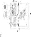
- FIG. 1 shows a block diagram of a system 100 for monitoring neurological brain activity, according to one exemplary embodiment.
- the system for monitoring neurological brain activity 100 may include an external unit 102 having inductive power coupling device 104 , an implant chip 106 having inductive power coupling device 108 , and a plurality of N electrodes 110 each having signal conducting means 111 for coupling to the implant chip 106 .
- the implant chip 106 may be placed between the surface of the subject's skull 114 and the skin 116 covering the skull 114 .
- the plurality of N electrodes 110 are coupled to the cortex region 120 of the subject's brain, while the signal conducting means 111 of the plurality of N electrodes are passed through both an opening 121 in the dura 118 covering the outer surface of the cortex 120 and an opening 123 created in the skull 114 .
- the plurality of N electrodes 110 and their corresponding signal conducting means 111 receive and transmit neurological signal activity (e.g., neural spike signals) from the cortex region 120 to the implant chip 106 .
- the implant chip 106 may then subsequently process and record any neurological signals (e.g., neural spikes) received from, for example, different areas r1, r2, r3 of the cortex region 120 .
- Data associated with the processed and recorded neurological signals can then be wirelessly transmitted by the implant chip 106 to the external unit 102 , which may be any type of computer device (e.g., laptop, desktop, tablet, mobile device, etc.).
- the external unit 102 causes a current to energize inductive power coupling device 104 .
- An electromagnetic field generated by the energized inductive power coupling device 104 then induces current within the inductive power coupling device 108 coupled to the implant chip 106 .
- the implant chip 106 can subsequently utilize this induced current to power a wireless transceiver located within the implant device 106 for data transmission/reception purposes.
- the external unit 102 may include software programming for further processing the data associated with the processed and recorded neurological signals (e.g., neural spikes). For example, the external unit 102 may pole the implant chip at regular intervals in order to receive and further process any neurological signals received from the cortex region 120 . According to another example, the external unit 102 may provide software updates and operational configurations to the implant device 106 .
- neurological signals e.g., neural spikes
- the external unit 102 may pole the implant chip at regular intervals in order to receive and further process any neurological signals received from the cortex region 120 .
- the external unit 102 may provide software updates and operational configurations to the implant device 106 .
- FIG. 2 shows a neural recording device 200 associated with FIG. 1 's exemplary system 100 for monitoring neurological brain activity, according to one embodiment.
- the neural recording device 200 includes both scan mode and read mode circuits for detecting and recording neural spike signals associated with a subject's brain (e.g., FIG. 1 : cortex region 120 ).
- the scan mode and read mode circuits may contemplate using separate devices or circuits to provide the scan mode and read mode operations. Alternatively, however, the scan mode and read mode circuits may contemplate using common/shared devices or circuits during the scan mode and read mode operations.
- the scan mode circuit includes a plurality of M signal combining circuits 202 a - 202 m that each detect the occurrence of one or more neural spike signals occurring within a corresponding group of electrodes taken from the total of N electrodes coupled to the brain.
- signal combining circuit 202 a detects the occurrence of one or more neural spike signals occurring within a first group (i.e., Group 1) of 1 to C electrodes
- signal combining circuit 202 b detects the occurrence of one or more neural spike signals occurring within a second group (i.e., Group 2) of other 1 to C electrodes
- signal combining circuit 202 c detects the occurrence of one or more neural spike signals occurring within a third group (i.e., Group 3) of other 1 to C electrodes, etc.
- Each of the plurality of M signal combining circuits 202 a - 202 m aggregate the signals received from respective input electrodes 1 to C.
- signal combining circuit 202 a includes high-pass filters 204 a - 204 c , a switch control unit 206 , and a power combiner 208 . Accordingly, signals received from input electrodes 1 to C are each filtered in order to pass the higher frequency neural spike signals, while filtering other spurious unwanted signals.
- high-pass filter 204 a filters neural spike signals that may be received from electrode 1
- high-pass filter 204 b filters neural spike signals that may be received from electrode 2, etc.
- high-pass filter 204 c filters neural spike signals that may be received from electrode C.
- the filtered outputs from the high-pass filters 204 a - 204 c are coupled to the switch control unit 206 , which enables or inhibits the transmission of the filtered outputs to the power combiner 208 .
- the power combiner 208 may then couple any of the neural spikes signals received from high-pass filters 204 a - 204 c to a single output O/P 1 .
- the power combiner 208 output O/P 1 thus enables the aggregation of any neural spike activity within the group of 1 to C electrodes regardless of whether only a single neural spike signal is received (e.g., neural spike received from only electrode 1), a few neural spike signals are received (e.g., neural spikes received from electrodes 1, 3, and 6), or all the neural spike signals are received (e.g., neural spikes received from every electrode 1 to C).
- Signal combining circuits 202 b - 202 m may also include the same or similar high-pass filters, switch control units, and power combiners to that of signal combining circuit 202 a described above.
- the scan mode circuit may also include a plurality of M neural signal detection circuits 210 a - 210 m that are each coupled to a respective one of the signal combining circuits 202 a - 202 m .
- neural signal detection circuit 210 a is coupled to signal combining circuit 202 a
- neural signal detection circuit 210 b is coupled to signal combining circuit 202 b
- neural signal detection circuit 210 c is coupled to signal combining circuit 202 c , etc.
- M neural signal detection circuits 202 a - 202 m are utilized, whereby each of the M neural signal detection circuits 210 a - 210 m detect the occurrence of any neural spike signals output from a respective one of the M signal combining circuits 202 a - 202 m to which it is coupled.
- neural signal detection circuit 210 a detects the occurrence of any neural spike signals output from signal combining circuit 202 a
- neural signal detection circuit 210 b detects the occurrence of any neural spike signals output from signal combining circuit 202 b
- neural signal detection circuit 210 c detects the occurrence of any neural spike signals output from signal combining circuit 202 c , etc.
- Each of the plurality of M neural signal detection circuits 210 a - 210 m may include a filtering and signal amplification circuit 212 (i.e., a preprocessing stage) and an analog-to-digital (A/D) convertor circuit 214 coupled to the filtering and signal amplification circuit 212 .
- the filtering and signal amplification circuit 212 may include a bandpass filter that is configured to pass a range of frequency components corresponding to the presence of neural spike signals, while suppressing other unwanted spurious signals (e.g., noise reduction). Any neural spike signals passed by the bandpass filter are then amplified by an amplifier circuit prior to being coupled to and received by the analog-to-digital (A/D) convertor circuit 214 .
- any filtered and amplified neural spike signals are converted to digitized neural spike signals.
- detected neural spike signals are converted into a digital format for facilitating a read mode operation of the neural recording device 200 . Accordingly, during the read mode, one or more neural spike signals present on all of the 1 to C electrodes associated with each of the M groups exhibiting a detected spike signal are recorded for further neurologically-related analysis, as described in more detail in the following paragraphs. As such, each of the M groups that do not have any detected neural spike signals are not considered for signal recording.
- the analog-to-digital (A/D) convertor circuit 214 may contemplate the use of a digital threshold comparison capability, whereby the digitized signals are compared with a digital threshold value in order to ensure that neural spikes, and not an unwanted signal components, have been detected and digitized.
- a digital threshold comparison capability can be incorporated within other circuitry/devices (e.g., DSP 218 ) associated with the neural recording device 200 .
- the read mode circuit records all neural spike signals present within any one of the M groups of electrodes where neural spike activity is detected by the scan mode circuit.
- a neural spike signal is detected on at least one of the electrodes within one of the M groups of electrodes, all of the electrodes within that group are routed through for signal recordation. Accordingly, routing and signal recordation is only applied to groups within the M groups where neural signals are detected, while signal routing and recordation is suspended for any of the groups within the M groups with no detected neural signal activity.
- routing and recordation of neural signals from the N electrodes can be achieved using a reduced number of M channels.
- the read mode circuit may include a switch matrix 216 and a digital signal processor (DSP) 218 .
- the read mode circuit may additionally include a telemetry and data storage unit 220 .
- the N electrodes coupled to the brain are also received as inputs to the switch matrix 216 .
- the switch matrix 216 has a reduced number of M outputs O/P m that are also coupled to the plurality of M neural signal detection circuits 210 a - 210 m associated with the scan mode circuit.
- the illustrated exemplary embodiment includes a circuit/device/component (i.e., neural signal detection circuits 210 a - 210 m ) that can form part of both the read mode circuit and the scan mode circuit.
- the M outputs of the switch matrix 216 may be coupled to M other neural signal detection circuits (not shown) that operate in a similar or identical manner to that of neural signal detection circuits 210 a - 210 m .
- any neural spike signals routed to the M outputs of the switch matrix 216 are filtered, amplified, and digitized (i.e., front end processing) by a respective one of the plurality of M neural signal detection circuits 210 a - 210 m.
- the DSP 218 may include any circuit capable of processing digital signals (e.g., neural signals, etc.) and generating commands for the execution of the neural recording device 200 operability.
- the DSP 218 may initiate, via a read control signal 203 , the routing operation of the switch matrix 216 based on the scan circuit detecting which groups of the M groups are exhibiting neural switch activity.
- the DSP 218 may active and deactivate the operation of the M signal combining circuits 202 a - 202 m and consequently the scan control circuit, via a scan control signal 201 .
- neural signals routed to switch outputs O/P m are detected and sent to the DSP 218 from the neural signal detection circuits 210 a - 210 m .
- the neural spike activity is detected on only signal combining circuit 202 a (Group 1) and signal combining circuit 202 b (Group 2)
- the signals associated with the 1 to C electrodes coupled to combining circuits 202 a and 202 b are routed to the switch matrix 216 outputs O/P m .
- a total of 16 electrodes corresponding to the inputs of both combining circuits 202 a , 202 b are routed to 16 outputs of the switch's M outputs O/P m .
- These 16 outputs are then processed by 16 neural signal detection circuits, whereby the processed outputs from these 16 neural signal detection circuits are received and recorded by the DSP 218 .
- the recording process may include storing the neural spike digital values of the routed 1 to C electrodes corresponding to the one or more signal combining circuits that exhibited neural spike activity during the scan mode.
- the DSP 216 stores the digital values associated with any of the neural spike signals detected on the 16 input electrodes of combining circuits 202 a and 202 b .
- the DSP 218 may store the neural spike digital values either within memory located on the DSP 218 , or alternatively, the DSP 218 may forward this data to the data storage and telemetry unit 220 .
- the recording process may also include storing additional information associated with each of the neural spike digital values. For example, data corresponding to each neural signal's time/date of recording (e.g., Mar. 31, 2016 at 10:30 AM) and electrode number (e.g., electrode 1006 ) may be stored with each of the neural spike digital values.
- the stored data corresponding to each neural signal's time/date of recording (e.g., Mar. 31, 2016 at 10:30 AM), electrode number (e.g., electrode 1006 ), and digital value may be transmitted via the telemetry functionality of unit 220 .
- the DSP 218 may include an embedded transceiver circuit, whereby the stored data corresponding to each neural signal's time/date of recording (e.g., Mar. 31, 2016 at 10:30 AM), electrode number (e.g., electrode 1006 ), and digital value may be transmitted using such a transceiver.
- both the telemetry/data storage unit 220 and the DSP's 218 transceiver can provide simultaneous transmission means for, among other things, each neural signal's time/date of recording (e.g., Mar. 31, 2016 at 10:30 AM), electrode number (e.g., electrode #1006), and digital value.
- each neural signal's time/date of recording e.g., Mar. 31, 2016 at 10:30 AM
- electrode number e.g., electrode #1006
- digital value e.g., digital value
- the throughput of neural spike data transmitted from the neural recording device 200 to the external unit 102 ( FIG. 1 ) can be dynamically increased to facilitate real-time monitoring of neurological activity.
- scan mode and read mode circuits have been described using the exemplary embodiment of neural recording device 200 , it will be appreciated that such scan and read mode functionality can be implemented using alternative hardware, software, firmware, or any combination thereof.
- FIGS. 3A-3D are flow diagrams associated with the operation of a neural recording system, according to one exemplary embodiment.
- the following operational description of a neural recording system is facilitated with the aid of the exemplary neural recording system of FIG. 2 , although any other hardware, software, or hardware/software-based neural recording system may be contemplated.
- a finite number of N electrodes to be processed are received.
- the N electrodes ( FIG. 2 ) are received by the signal combining circuits 202 a - 202 m ( FIG. 2 ) and the switch matrix 216 ( FIG. 2 ).
- a combined signal output (P) for each of the M groups is generated by filtering each input channel (C) within the group and combining the output signal of each of the filtered channels.
- O/P 1 FIG. 2
- Combined signal outputs O/P 2 -O/P m . ( FIG. 2 ) for the remaining combining circuits are thus generated in the same or similar manner.
- M outputs O/P 1 -O/P m . ( FIG. 2 ) are generated from the signal combining circuits 202 a - 202 m ( FIG. 2 ).
- the combined signal output (P) of each one of the M groups are scanned in order to determine the presence of one or more neural spike signals associated with each of the M groups. For example, using neural signal detection circuits 210 a - 210 m ( FIG. 2 ), the combined signal outputs O/P 1 -O/P m . ( FIG. 2 ) received from each of the respective combining circuits 202 a - 202 m ( FIG. 2 ) are scanned in order to determine the presence of one or more neural spike signals. For example, neural signal detection circuit 210 a ( FIG. 2 ) determines whether one or more neural spike signals can be detected from the output O/P 1 of combining circuit 202 a ( FIG.
- neural signal detection circuit 210 b determines whether one or more neural spike signals can be detected from the output O/P 2 of combining circuit 202 b ( FIG. 2 ), neural signal detection circuit 210 c ( FIG. 2 ) determines whether one or more neural spike signals can be detected from the output O/P 3 of combining circuit 202 c ( FIG. 2 ), etc.
- Neural signal detection circuit 210 a determines the presence of one or more neural spike signals by bandpass filtering, amplifying, and digitizing signals that are received from the output O/P 1 ; neural signal detection circuit 210 b ( FIG.
- neural signal detection circuit 210 c determines the presence of one or more neural spike signals by bandpass filtering, amplifying, and digitizing signals that are received from the output O/P 2 ; neural signal detection circuit 210 c ( FIG. 2 ) determines the presence of one or more neural spike signals by bandpass filtering, amplifying, and digitizing signals that are received from the output O/P 3 , etc. At these outputs O/P 1 -O/P m . ( FIG. 2 ), the digitized signals having a value above a certain threshold (e.g., above the noise level or spurious signals conducted on the electrodes) may thus correspond to detected neural spike signals.
- a certain threshold e.g., above the noise level or spurious signals conducted on the electrodes
- a neural spike signal is present at any of the combined signal outputs. For example, based on the scanning described above in relation to process 308 , it is determined whether a neural spike signal or signals is present on one or more of the combined signal outputs O/P 1 -O/P m . ( FIG. 2 ). For example, based on the scanning, it may be determined that neural spike signals are present on only O/P 1 , O/P 2 , and O/P 3 ( FIG. 2 ). If no neural spike signals are present on any of the outputs O/P 1 -O/P m . ( FIG. 2 ), then processing returns to 306 and 308 , where signal combining and scanning is continued until neural spike signal activity on any of the combined outputs O/P 1 -O/P m . ( FIG. 2 ) is detected.
- neural spike signals from each of the channels (C) corresponding to S of the M groups where the presence of one or more neural spike signals was detected during the scanning are preprocessed (e.g., amplified and filtered), whereby S ⁇ M.
- one or more neural spike signals may be detected at only output O/P 1 of combining circuit 202 a ( FIG. 2 ), O/P 2 of combining circuit 202 b ( FIG. 2 ), and O/P 3 of combining circuit 202 c ( FIG. 2 ).
- the DSP 218 FIG. 2
- each of combining circuits 202 a , 202 b , and 202 c include ‘8’ electrodes that are routed by the switch 216 . Therefore, a total of ‘24’ electrodes (3 ⁇ 8) are routed to ‘24’ corresponding neural signal detection circuits 210 a - 210 m ( FIG. 2 ) for preprocessing, whereby electrodes conducting neural spike signals are filtered and amplified.
- a reduced number of electrodes are processed at any given time, since routing and recording are initiated only for groups of electrodes exhibiting signal activity.
- the preprocessed neural spike signals from each of the channels (C) corresponding to the S groups identified from the M groups are digitized and may be further processed (e.g., whereby M-S groups are inactive (i.e., no neural spike activity).
- M-S groups are inactive (i.e., no neural spike activity).
- the total of ‘24’ electrodes (3 ⁇ 8) that are routed to the ‘24’ corresponding neural signal detection circuits 210 a - 210 m ( FIG. 2 ) are digitized and stored following the filtering and amplification (i.e., preprocessing).
- preprocessing may not be required.
- neural spike signals that are routed are directly digitized and stored.
- the processing can include not only the storing of the digitized neural signals (i.e., digital values), but also providing several other actions, such as but not limited to, adding metadata (e.g., timestamp, date, electrode information, etc.), adding communication protocol information, and controlling the data transmission of the stored digitized neural signals.
- the scanning and recording process may be conditionally reconfigured to include certain groups of electrodes that are in a read only mode (continuous routing and recording), while other groups of electrodes are assigned as operating in the scan and read mode configuration described in relation to FIG. 3A .
- the conditional reconfiguration can be overridden in favor of a manual reconfiguration process where a user may determine which groups of electrodes are in a read only mode (continuous routing and recording), and what groups of electrodes are to be assigned as operating in the scan and subsequent read mode configuration.
- continuously routed means that the K groups are recorded without the groups being scanned for the detection of a neural spike signal prior to being routed through for recording purposes.
- combining circuits e.g., FIG. 2 : 202 a - 202 m
- neural signal detection circuits e.g., FIG. 2 : 210 a - 210 m
- combining circuits e.g., FIG. 2 : 202 a - 202 m
- neural signal detection circuits e.g., FIG. 2 : 210 a - 210 m
- a constant recording of user-selected groups may be adopted without the delay of scanning and then reading the neural spike signals. Since the conditional process of 318 allocates a predetermined allocation of J and K groups, process 320 allows a user to vary the designation of the J and K groups based on further observation of the neural activity.
- continuously routed means that the K′ groups are recorded without the groups being scanned for the detection of a neural spike signal prior to being routed through for recording purposes.
- combining circuits e.g., FIG. 2 : 202 a - 202 m
- neural signal detection circuits e.g., FIG. 2 : 210 a - 210 m
- combining circuits e.g., FIG. 2 : 202 a - 202 m
- neural signal detection circuits e.g., FIG. 2 : 210 a - 210 m
- a constant recording of user-selected groups may be adopted without the delay of scanning and then reading the neural spike signals. Since the conditional process of 324 allocates a predetermined allocation of J′ and K′ groups, process 326 allows a user to vary the designation of the J′ and K′ groups based on further observation of the neural activity.
- the operation follows that of FIG. 3A (see Label B).
- the operation returns to that of FIG. 3A , as indicated by label B.
- the exemplary threshold of process 316 is for capturing relatively smaller regions of neural activity on a continuous basis, while conversely, the threshold of process 322 is for capturing relatively larger regions of neural activity on a continuous basis.
- the operation is governed by a scan mode followed by a read mode that responds to the results of the scan mode.
- FIG. 3C shows the process steps of providing an embodiment for simultaneously scanning and reading neural signal activity on the electrodes, once electrode groups J and K have been designated based on satisfying threshold condition 316 illustrated in FIG. 3B .
- Processes 330 - 338 thus correspond to a scan mode of operation for the electrodes of group J, while processes 340 - 342 are associated with simultaneously reading group K electrodes during the scanning of group J.
- a combined signal output (P′) for each of the J groups is generated by filtering each channel (C) and combining the output signal of each filtered channel.
- P′ a combined signal output for each of the J groups
- C channel
- a combined signal output (P′) for each of the J groups is generated by filtering each channel (C) and combining the output signal of each filtered channel.
- the combined signal output (P′) of each one of the J groups are scanned in order to determine the presence of a neural spike signal associated with each of the J groups.
- At 334 it is determined whether at least one neural spike signal is detected during the scanning ( 332 ) of, for example, outputs O/P 4 -O/P m . ( FIG. 2 ). If no neural spike signal is detected, the process returns to 330 . However, if at least one neural spike signal is detected from S′ of the J groups, at 336 neural spike signals from each of the channels (C) corresponding to the S′ groups where the presence of one or more neural spike signals were detected during the scanning are preprocessed (e.g., filtered and amplified).
- the neural spike signals of the S′ groups (e.g., Group 4-Group 6) that are preprocessed (e.g., filtered and amplified) using twenty-four of the neural signal detection circuits 210 a - 210 m ( FIG. 2 ) are then digitized by the A/D conversion units within these three neural signal detection circuits. Following this conversion, other processing may occur such as, but not limited, storing the digitized neural spike signals detected from all the channels of the S′ groups (e.g., Group 4-Group 6). According to other processing, the digitized neural spike signals may be packetized for WiFi, Bluetooth, or other radio transmission.
- other processing may occur such as, but not limited to, storing the digitized neural spike signals detected from all the channels of the K groups (e.g., Group 1-Group 3).
- the digitized neural spike signals may be packetized for WiFi, Bluetooth, or other radio type transmissions.
- FIG. 3D shows the process steps of providing an embodiment for simultaneously scanning and reading neural signal activity on the electrodes, once electrode groups J′ and K′ have been designated based on satisfying threshold condition 322 illustrated in FIG. 3B .
- Processes 346 - 354 thus correspond to a scan mode of operation for the electrodes of group J′, while processes 356 - 358 are associated with simultaneously reading group K′ electrodes during the scanning of group J′.
- a combined signal output (P′′) for each of the J′ groups is generated by filtering each channel (C) and combining the output signal of each filtered channel.
- P′′ a combined signal output for each of the J′ groups
- the combined signal output (P′′) of each one of the J groups are scanned in order to determine the presence of a neural spike signal associated with each of the J groups.
- At 350 it is determined whether at least one neural spike signal is detected during the scanning ( 332 ) of, for example, outputs O/P 7 -O/P m . ( FIG. 2 ). If no neural spike signal is detected, the process returns to 346 . However, if at least one neural spike signal is detected from S′′ of the J′ groups, at 352 neural spike signals from each of the channels (C) corresponding to the S′′ groups where the presence of one or more neural spike signals were detected during the scanning are preprocessed (e.g., filtered and amplified).
- the neural spike signals of the S′′ groups (e.g., Group 7-Group 8) that are preprocessed (e.g., filtered and amplified) using sixteen of the neural signal detection circuits 210 a - 210 m ( FIG. 2 ) are then digitized by the A/D conversion units within these three neural signal detection circuits. Following this conversion, other processing may occur such as, but not limited, storing the digitized neural spike signals detected from all the channels of the S′′ groups (e.g., Group 7-Group 8). According to other processing, the digitized neural spike signals may be packetized for WiFi, Bluetooth, or other radio transmission.
- other processing may occur such as, but not limited to, storing the digitized neural spike signals detected from all the channels of the K′ groups (e.g., Group 1-Group 6).
- the digitized neural spike signals may be packetized for WiFi, Bluetooth, or other radio type transmissions.
- the allocation of groups for simultaneous read mode and scan mode operations can be configured based on detected neural spike signal activities. In other embodiments, however, the allocation of groups for simultaneous read mode and scan mode operations can be responsive to which groups, and thus what area or areas of the brain, is exhibiting neural spike signal activity.
- Signal combining circuit 400 can be used to implement each of the plurality of M signal combining circuits 202 a - 202 m within the neural recording device 200 of FIG. 2 .
- the circuit 400 includes a plurality of signal combining circuits 402 a - 402 m , a switch control unit 410 , and a final stage power combiner unit 412 .
- the plurality of signal combining circuits 402 a - 402 m can each include a plurality of high pass filters 404 a - 404 c , a switch control unit 406 , and a power combiner unit 408 .
- the neural signals are received by the plurality of inputs 401 , whereby each input from the plurality of inputs 401 is coupled in series to a high pass filter in the respective signal combining circuits 402 a - 402 m .
- inputs 1 to C are each coupled in series with high pass filters 404 a - 404 c .
- inputs 1 to C are each coupled in series with the high pass filters within those signal combining circuits 402 b - 402 m.
- Each high pass filter associated with signal combining circuits 402 a - 402 m is configured to output high-frequency signals (i.e. neural spikes), which may then be passed to their respective switch control units.
- high-frequency signals i.e. neural spikes
- high pass filters 404 a - 404 c may then be passed to switch control unit 406 .
- the neural spike signals may then be passed onto power combiner unit 408 when a corresponding switch within the switch control unit 406 is actuated to a closed circuit position (i.e., enabled).
- the high pass filters, switch control units, and power combiner units associated with the other signal combining circuits 402 b - 402 m are identical to signal combining circuit 402 a , and thus operate in the same manner. Accordingly, within each of the signal combining circuits 402 a - 402 m , filtered neural spike signals received from inputs or channels 1 to C are combined by respective power combiner units and output to switch control unit 410 . Switch control unit 410 then receives one or more combined neural spike signals that are output from each of the signal combining circuits 402 a - 402 m .
- switch control unit 410 controls the transmission of the combined neural spike signals to power combiner 412 , whereby under the control of switch control unit 410 , the output of any one or more of the signal combining circuits 402 a - 402 m can be further combined at the output O/P T of power combiner 412 .
- the combined output O/P G1 from signal combining circuit 402 a may be transmitted to power combiner 412 under the control of switch control unit 410
- the combined output O/P G2 from signal combining circuit 402 b may be transmitted to power combiner 412 under the control of switch control unit 410
- the combined output O/P G3 from signal combining circuit 402 c may be transmitted to power combiner 412 under the control of switch control unit 410
- the combined output O/P G4 from signal combining circuit 402 d may be transmitted to power combiner 412 under the control of switch control unit 410
- the combined output O/P GY from signal combining circuit 402 m may be transmitted to power combiner 412 under the control of switch control unit 410 .
- any combination of these outputs O/P G1 -O/P GY can be combined at the output O/P T of the final stage power combiner 412 using the final stage switch control unit 410 .
- DSP 218 FIG. 2
- DSP 218 may generate a configuration signal that enables the predetermined combining of any combination of outputs O/P G1 -O/P GY .
- scanning for neural spike signals within a given area of the brain cortex can be adjusted to be more or less coarse by configuring the number of outputs from the respective signal combining circuits 402 a - 402 m that are combined.
- signal combining circuit 400 can be incorporated within signal combining circuit 202 a ( FIG. 2 ) or any other one or more of the other signal combining circuits 202 b - 202 m ( FIG. 2 ) of the neural recording device 200 of FIG. 2 .
- switch control unit 410 may be programmed to only enable the output O/P G1 of signal combining circuit 402 a to be sent to the power combiner 412 and thus provide the output O/P T of circuit 400 .
- the power combiner 412 Since in the given example, the only output received by the power combiner 412 is output O/P G1 from signal combining circuit 402 a , the power combiner 412 has no other signal or signals to combine at its output O/P T .
- the first configuration can be utilized to generate a single output (i.e., one of O/P G1 -O/P GY ) from one of the plurality of signal combining circuits 402 a - 402 m of circuit 400 .
- circuit 400 facilitates the operation of the signal combining circuits 202 a - 202 m of FIG. 2 , whereby, for example, signal combining circuit 402 a is used to scan neural spike signal activities within region r1 ( FIG. 1 ) of the cortex 110 ( FIG. 1 ).
- switch control unit 410 may be programmed to enable both the output O/P G1 of signal combining circuit 402 a and the output O/P G2 of signal combining circuit 402 b to be sent to the power combiner 412 for generating the output O/P T of circuit 400 .
- outputs O/P G1 and O/P G2 are received and combined by the power combiner 412 to form the combined output O/P T of circuit 400 .
- circuit 400 facilitates an alternative operation of the signal combining circuits 202 a - 202 m of FIG.
- signal combining circuits 402 a and 402 b are used to scan neural spike signal activities within larger region r′1 ( FIG. 1 ) of the cortex 110 ( FIG. 1 ).
- a single signal combining circuit 402 a can be used to scan for neural spike signal activity over an increase area of the cortex.
- This configuration may be utilized in scenarios where there is reduced neural spike signal activity over a given area of the cortex and, therefore, signal processing efficiency is facilitated by monitoring a larger group of electrodes.
- some of the of M outputs include a combination of more of the N inputs, while other ones of the M outputs include an aggregation of less of the N inputs.
- the larger group configurations enable the use of a reduced number of neural signal detection circuits, thus contributing to power consumption savings facilitated by turning off unused neural signal detection circuits.
- circuit 400 is used in neural recording device 200 ( FIG. 2 )
- signal combining circuits 402 a and 402 b being used to scan neural spike signal activities over a larger region r′1 ( FIG. 1 ) of the cortex 110 ( FIG. 1 )
- a single neural signal detection circuit such as neural signal detection circuit 210 a may be utilized. Consequently, neural signal detection circuit 210 b may be switched off.
- Signal combining circuit 500 can be used to implement each of the plurality of M signal combining circuits 202 a - 202 m within the neural recording device 200 of FIG. 2 .
- the exemplary embodiment of signal combining circuit 500 can be used to implement each of the signal combining circuits 402 a - 402 m ( FIG. 4 ) within signal combining circuit 400 ( FIG. 4 ).
- the circuit 500 can include a plurality of capacitors 502 a - 502 c , input switches 504 a - 504 c , a resistive unit 510 , and an output switch 506 .
- the capacitors 502 a - 502 c are respectively in series with input switches 504 a - 504 c .
- capacitor 502 a is coupled in series with switch 504 a
- capacitor 502 b is coupled in series with switch 504 b
- capacitor 502 c is coupled in series with switch 504 c .
- the output of each of the switches 504 a - 504 c are electrically coupled to both switch 506 and resistive unit 510 , as indicated at A.
- resistive unit 510 is also connected to ground, as indicated at B.
- a neural spike signal NSS received at input 501 a is passed through the high-pass filter formed by capacitor 502 a and resistive unit 510 , while other signals outside the frequency band of this filter are attenuated.
- the resistive unit 510 may need a large resistance value (e.g. 100s of Mega-Ohms or more) to accomplish the requisite filtering.
- the resistive unit 510 can thus be implemented with transistor-based pseudo resistors capable of generating a higher resistance per chip area compared to fabricating, for example, passive resistive components.
- Signals are generated based on different voltages generated by the resistive unit 510 based on the neural spike signals received from inputs 501 . Accordingly, as neural spike signals are received by more inputs, an increase in voltage is generated by the resistive unit 510 at A. For example, if neural spike signals are received at input 501 a , a voltage V 1 is generated. However, if neural spike signals are received at inputs 501 a , 501 b , and 501 c , an increased current from these aggregate neural spike signal generates a voltage V 2 , whereby V 2 >V 1 . Thus, different voltage levels are generated as a function of the combined neural spike signals received from inputs 501 .
- FIG. 6 shows another neural recording system 600 associated with FIG. 1 's system for monitoring neurological brain activity, according to another exemplary embodiment.
- the various components of neural recording system 600 are identical to, and operate in the same or similar manner with, the neural recording system 200 of FIG. 2 .
- two (2) signal combining circuits 602 a - 602 b are coupled to two (2) neural signal detection circuits 610 a - 610 b
- a plurality of other (3 . . . C) neural signal detection circuits 610 c - 610 m are coupled directly to the switch matrix 616 output without being utilized in the scan mode operation.
- the neural recording device 600 includes both scan mode and read mode circuits for detecting and recording neural spike signals associated with a subject's brain (e.g., FIG. 1 : cortex region 120 ).
- the scan mode and read mode circuits may contemplate using separate devices or circuits to provide the scan mode and read mode operations. Alternatively, however, the scan mode and read mode circuits may contemplate using common/shared devices or circuits during the scan mode and read mode operations.
- the scan mode circuit includes signal combining circuits 602 a - 602 b that each detect the occurrence of one or more neural spike signals occurring within a corresponding group of electrodes taken from the total of N electrodes coupled to the brain.
- signal combining circuit 602 a detects the occurrence of one or more neural spike signals occurring within the first group (i.e., Group 1) of 1 to C electrodes
- signal combining circuit 602 b detects the occurrence of one or more neural spike signals occurring within the second group (i.e., Group 2) of other 1 to C electrodes.
- Each of the signal combining circuits 602 a - 602 b aggregate the signals received from respective input electrodes 1 to C.
- signal combining circuit 602 a includes high-pass filters 604 a - 604 c , a switch control unit 606 , and a power combiner 608 .
- signals received from input electrodes 1 to C are each filtered in order to pass the higher frequency neural spike signals, while filtering other spurious unwanted signals.
- the filtered outputs from the high-pass filters 604 a - 604 c are coupled to the switch control unit 606 , which enables or inhibits the transmission of the filtered outputs to the power combiner 608 .
- the power combiner 608 may then couple any of the neural spikes signals received from high-pass filters 604 a - 604 c to a single output O/P 1 .
- the power combiner 608 output O/P 1 thus enables the aggregation of any neural spike activity within the group of 1 to C electrodes regardless of whether only a single neural spike signal is received (e.g., neural spike received from only electrode 1), a few neural spike signals are received (e.g., neural spikes received from electrodes 1, 3, and 6), or all the neural spike signals are received (e.g., neural spikes received from electrodes 1 to C).
- Signal combining circuit 602 b may also include the same or similar high-pass filters, switch control units, and power combiners to that of signal combining circuit 602 a described above.
- the signal combining circuits 602 a - 602 b may each receive a different number of input electrodes.
- combining circuit 602 a receives input electrodes 1 to C (e.g., electrodes 1-32)
- combining circuit 602 b can receive input electrodes 1 to C′ (e.g., electrodes 1-64).
- more electrodes e.g., electrodes 1-64) may be assigned to a combining circuit for a given area A r of the cortex where less neurological signal activity is expected.
- Electrodes 1-32 may be assigned to a combining circuit for the same give area A r of the cortex where more neurological signal activity is expected.
- the assignment of electrodes to combining circuits can be determined based on neural signal detection granularity requirements.
- the scan mode circuit may also include a plurality of M neural signal detection circuits 610 a - 610 m , some of which (i.e., 610 a - 610 b ) are each coupled to a respective one of the signal combining circuits (i.e., 602 a - 602 b ), while others (i.e., 610 c - 610 m ) are coupled directly to the switch matrix for the read-mode operation.
- neural signal detection circuit 610 a is coupled to signal combining circuit 602 a
- neural signal detection circuit 610 b is coupled to signal combining circuit 602 b
- neural signal detection circuit 610 a detects the occurrence of any neural spike signals output from signal combining circuit 602 a
- neural signal detection circuit 610 b detects the occurrence of any neural spike signals output from signal combining circuit 602 b.
- Each of the plurality of neural signal detection circuits 610 a - 610 m may include a filtering and signal amplification circuit 612 and an analog-to-digital (A/D) convertor circuit 614 coupled to the filtering and signal amplification circuit 612 .
- the filtering and signal amplification circuit 612 may include a bandpass filter that is configured to pass a range of frequency components corresponding to the presence of neural spike signals, while suppressing other unwanted spurious signals (e.g., noise). Any neural spike signals passed by the bandpass filter are then amplified by an amplifier circuit prior to being coupled to and received by the analog-to-digital (A/D) convertor circuit 614 .
- any filtered and amplified neural spike signals are converted to digitized neural spike signals.
- detected neural spike signals are converted into a digital format for facilitating read/scan mode operations of the neural recording device 600 . Accordingly, during the read mode, one or more neural spike signals present on all of the 1 to C electrodes associated with either one of the two (2) groups are recorded for further neurologically-related analysis, as described in more detail in the following paragraphs.
- the analog-to-digital (A/D) convertor circuit 614 may contemplate the use of a digital threshold comparison capability, whereby the digitized signals are compared with a digital threshold value in order to ensure that neural spikes, and not an unwanted signal components, have been detected and digitized.
- a digital threshold comparison capability can be incorporated within other circuitry/devices (e.g., DSP 618 ) associated with the neural recording device 600 .
- the read mode circuit records all neural spike signals present within any one of the two groups (i.e., Group 1 or Group 2) of electrodes where neural spike activity is detected by the scan mode circuit.
- a neural spike signal is detected on at least one of the electrodes within one of the two groups of electrodes (e.g., Group 1)
- all of the electrodes within that group are routed through for signal recordation.
- routing and signal recordation e.g., digitization, formatting, storage, etc.
- routing and recordation is applied to one of the two groups (e.g., Group 1) where neural signals are detected, while signal routing and recordation is suspended for the other group (e.g., Group 2) within the two (2) groups with no detected neural signal activity.
- a reduced number of C channels e.g. 50% reduction).
- the read mode circuit may include a switch matrix 616 and a digital signal processor (DSP) 618 .
- the read mode circuit may additionally include a telemetry and data storage unit 620 .
- the N electrodes coupled to the brain are also received as inputs to the switch matrix 616 .
- the switch matrix 616 has a reduced number outputs (e.g., 1 to C) that are also coupled to the plurality of neural signal detection circuits 610 a - 610 m , some of which (i.e., 610 a - 610 b ) are associated with the scan mode circuit.
- the illustrated exemplary embodiment includes a first circuit/device/component (i.e., neural signal detection circuits 210 a - 210 b ) that can form part of both the read mode circuit and the scan mode circuit, while a second circuit/device/component (i.e., neural signal detection circuits 210 c - 210 m ) is part of the read mode circuit.
- a first circuit/device/component i.e., neural signal detection circuits 210 a - 210 b
- a second circuit/device/component i.e., neural signal detection circuits 210 c - 210 m
- the 3-C outputs of the switch matrix 616 are coupled to neural signal detection circuits 610 c - 610 m that operate in a similar or identical manner to that of neural signal detection circuits 610 a - 610 b .
- any neural spike signals routed to the 1-C outputs of the switch matrix 216 are filtered, amplified, and digitized (i.e., front end processing) by a respective one of the plurality of 1-C neural signal detection circuits 610 a - 610 m.
- the DSP 618 may include any circuit capable of processing digital signals (e.g., neural signals, etc.) and generating commands for the execution of the neural recording device 600 operability.
- the DSP 618 may initiate, via a read control signal 603 , the routing operation of the switch matrix 616 based on the scan circuit detecting which groups of the two groups are exhibiting neural switch activity.
- the DSP 618 may activate and deactivate the operation of the signal combining circuits 602 a - 602 b and consequently the scan control circuit, via a scan control signal 601 .
- neural signals routed to switch outputs 1-C are detected and sent to the DSP 618 from the neural signal detection circuits 610 a - 610 m .
- the neural spike activity is detected on only signal combining circuit 602 a (Group 1)
- the signals associated with the 1 to C electrodes coupled to combining circuit 602 a is routed to the switch matrix 616 output 1-C.
- 8 electrodes corresponding to the input of combining circuit 202 a are routed to 8 outputs of the switch's 616 outputs.
- These 8 outputs are then processed by 8 neural signal detection circuits, whereby the processed outputs from these 8 neural signal detection circuits are received and recorded by the DSP 618 .
- the recording process may include storing the neural spike digital values of the routed 1 to C electrodes corresponding to the one of the signal combining circuits that exhibited neural spike activity during the scan mode.
- the DSP 616 stores the digital values associated with any of the neural spike signals detected on the 8 input electrodes of combining circuit 602 a .
- the DSP 618 may store the neural spike digital values either within memory located on the DSP 618 , or alternatively, the DSP 618 may forward this data to the data storage and telemetry unit 620 .
- the recording process may also include storing additional information associated with each of the neural spike digital values. For example, data corresponding to each neural signal's time/date of recording (e.g., Mar. 31, 2016 at 10:30 AM) and electrode number (e.g., electrode #1006) may be stored with each of the neural spike digital values.
- the stored data corresponding to each neural signal's time/date of recording (e.g., Mar. 31, 2016 at 10:30 AM), electrode number (e.g., electrode #1006), and digital value may be transmitted via the telemetry functionality of unit 620 .
- the DSP 618 may include an embedded transceiver circuit, whereby the stored data corresponding to each neural signal's time/date of recording (e.g., Mar. 31, 2016 at 10:30 AM), electrode number (e.g., electrode #1006), and digital value may be transmitted using such a transceiver.
- both the telemetry/data storage unit 620 and the DSP's 618 transceiver can provide simultaneous transmission means for, among other things, the each neural signal's time/date of recording (e.g., Mar. 31, 2016 at 10:30 AM), electrode number (e.g., electrode #1006), and digital value.
- the throughput of neural spike data transmitted from the neural recording device 600 to the external unit 102 ( FIG. 1 ) can be dynamically increased to facilitate real-time monitoring of neurological activity.
- Exemplary neural recording device 600 is an alternative embodiment, where the received electrodes are split into two groups as opposed to three or more groups, as with neural recording device 200 ( FIG. 2 ). Since each of the signal combining circuits can include more than two inputs (e.g., 128 electrodes), for signal recording purposes, more than two signal detection circuits (e.g., 128 detection circuits) are utilized. As such, two (2) detection circuits coupled to the two signal combining circuits are used along with an additional hundred and twenty-six (126) detection circuits dedicated for the signal recording.
- FIG. 7 is a flow diagram 700 associated with controlling the scan-mode and read-mode processes of a neural recording system, according to one exemplary embodiment.
- the corresponding processes of flow diagram 700 may be executed as a Neural Signal Recording Control (NSRC) program on any processing device, such as, for example, DSP 218 ( FIG. 2 ) or DSP 618 ( FIG. 6 ).
- NRC Neural Signal Recording Control
- FIG. 7 is described with the aid of the exemplary embodiment of FIG. 2 .
- a scan control signal for enabling the receiving of a plurality of M output signals is generated, where each of the plurality of M output signals are based on a combining of a plurality of input signals (i.e., signal groups) respectively received from a plurality of N electrodes coupled to the brain.
- a Scan Ctr signal 201 which is output from DSP 218 , enables the switch control units 206 within each of the plurality of M signal combining circuits 202 a - 202 m (Groups 1-M) by actuating them to a closed position.
- This switch enabling function allows the outputs O/P 1 -O/P m of the plurality of M signal combining circuits 202 a - 202 m (Groups 1-M) to be coupled to the plurality of M neural signal detection circuits 210 a - 210 m for the scan mode operation.
- digitized versions of the plurality of M output signals are received for detecting neural spike signals from one or more of the plurality of M output signals.
- the plurality of M neural signal detection circuits 210 a - 210 m pre-process (e.g., amplify and filter) and digitize any neural spike signals that are received from the respective outputs O/P 1 -O/P m of the plurality of M signal combining circuits 202 a - 202 m (Groups 1-M).
- a read control signal is generated for enabling the recording of neural spike signals received from all of the plurality of electrodes (i.e., signal groups) corresponding to any one or more of the plurality M output signals having detected neural spike signals.
- the scan mode receiving of the plurality of output signals is disabled by the scan control signal.
- a Read Ctr signal 203 which is output from DSP 218 , enables the switch matrix 216 to route all of the input signals associated with the one or more plurality of M signal combining circuits 202 a - 202 m (Groups 1-M) having the detected neural spike signals.
- the number of M output signals that can be routed is less than the total number of N electrodes coupled to the brain, thus providing an increased processing efficiency caused by having less scan-mode and read-mode channels relative to the received N electrodes (i.e., input channels).
- processes 708 - 714 correspond to partitioning the total of M outputs (for M groups) into J outputs (for J groups) that are scanned and then recorded based on the scanning, and M-J remaining outputs (for M-J remaining groups) that are directly recorded without any prior scanning.
- a scan control signal for enabling the receiving of a plurality of J output signals is generated, where each of the plurality of J output signals are based on a combining of a plurality of input signals (i.e., signal groups) respectively received from a group or subset of the plurality of N electrodes coupled to the brain.
- digitized versions of the plurality of J output signals are received for detecting neural spike signals from one or more of the plurality of J output signals.
- a first read control signal is generated for enabling the recording of neural spike signals received from all of the plurality of electrodes (i.e., signal groups) corresponding to any one or more of the plurality J output signals having the detected neural spike signals.
- the receiving of the plurality of output signals is disabled by the scan control signal.
- a second read control signal is generated for enabling a signal recording from a plurality of input signals received from a second group or subset (M-J) of the plurality of N electrodes, where the second group of the plurality of N electrodes (i.e., M-J electrodes) are respectively recorded via M-J output signals from the switch matrix.
- M-J second group or subset
- a total of 16 inputs are routed via the switch input 231 to switch output 233 .
- FIG. 8 shows a block diagram of the components of a data processing system 800 , 900 , that may be incorporated within a processing component such as 106 ( FIG. 1 ) and/or 108 ( FIG. 1 ) in accordance with an illustrative embodiment of the present invention. It should be appreciated that FIG. 8 provides only an illustration of one implementation and does not imply any limitations with regard to the environments in which different embodiments may be implemented. Many modifications to the depicted environments may be made based on design and implementation requirements.
- Data processing system 800 , 900 is representative of any electronic device capable of executing machine-readable program instructions.
- Data processing system 800 , 900 may be representative of a smart phone, a computer system, PDA, or other electronic devices.
- Examples of computing systems, environments, and/or configurations that may represented by data processing system 800 , 900 include, but are not limited to, personal computer systems, server computer systems, thin clients, thick clients, hand-held or laptop devices, multiprocessor systems, microprocessor-based systems, network PCs, minicomputer systems, and distributed cloud computing environments that include any of the above systems or devices.
- the data processing system 800 , 900 may include may include a set of internal components 800 and a set of external components 900 illustrated in FIG. 8 .
- the set of internal components 800 includes one or more processors 820 , one or more computer-readable RAMS 822 and one or more computer-readable ROMS 824 on one or more buses 826 , and one or more operating systems 828 and one or more computer-readable tangible storage devices 830 .
- the one or more operating systems 828 and programs such as neural signal recording control (NSRC) Program 801 (also see FIG. 7 ) and the processes of FIGS. 3A-3D can be stored on one or more computer-readable tangible storage devices 830 for execution by one or more processors 820 via one or more RAMS 822 (which typically include cache memory).
- NSRC neural signal recording control
- each of the computer-readable tangible storage devices 830 is a magnetic disk storage device of an internal hard drive.
- each of the computer-readable tangible storage devices 830 is a semiconductor storage device such as ROM 824 , EPROM, flash memory or any other computer-readable tangible storage device that can store a computer program and digital information.
- the set of internal components 800 also includes a R/W drive or interface 832 to read from and write to one or more portable computer-readable tangible storage devices 936 such as a CD-ROM, DVD, memory stick, magnetic tape, magnetic disk, optical disk or semiconductor storage device.
- the NSRC program 801 can be stored on one or more of the respective portable computer-readable tangible storage devices 936 , read via the respective R/W drive or interface 832 and loaded into the respective hard drive 830 .
- the set of internal components 800 may also include network adapters (or switch port cards) or interfaces 836 such as a TCP/IP adapter cards, wireless wi-fi interface cards, or 3G or 4G wireless interface cards or other wired or wireless communication links.
- NSRC program 801 and/or the processes of FIGS. 3A-3D can be downloaded from an external computer (e.g., server) via a network (for example, the Internet, a local area network or other, wide area network) and respective network adapters or interfaces 836 . From the network adapters (or switch port adaptors) or interfaces 836 , the NSRC program 801 and/or the processes of FIGS. 3A-3D are loaded into the respective hard drive 830 .
- the network may comprise copper wires, optical fibers, wireless transmission, routers, firewalls, switches, gateway computers and/or edge servers.
- the set of external components 900 can include a computer display monitor 920 , a keyboard 930 , and a computer mouse 934 .
- External component 900 can also include touch screens, virtual keyboards, touch pads, pointing devices, and other human interface devices.
- the set of internal components 800 also includes device drivers 840 to interface to computer display monitor 920 , keyboard 930 and computer mouse 934 .
- the device drivers 840 , R/W drive or interface 832 and network adapter or interface 836 comprise hardware and software (stored in storage device 830 and/or ROM 824 ).
Landscapes
- Health & Medical Sciences (AREA)
- Life Sciences & Earth Sciences (AREA)
- Engineering & Computer Science (AREA)
- Medical Informatics (AREA)
- Surgery (AREA)
- Biophysics (AREA)
- Biomedical Technology (AREA)
- Heart & Thoracic Surgery (AREA)
- Physics & Mathematics (AREA)
- Molecular Biology (AREA)
- Pathology (AREA)
- Animal Behavior & Ethology (AREA)
- General Health & Medical Sciences (AREA)
- Public Health (AREA)
- Veterinary Medicine (AREA)
- Neurology (AREA)
- Computer Networks & Wireless Communication (AREA)
- Measurement And Recording Of Electrical Phenomena And Electrical Characteristics Of The Living Body (AREA)
Abstract
Description
Claims (13)
Priority Applications (6)
| Application Number | Priority Date | Filing Date | Title |
|---|---|---|---|
| US15/695,408 US10694964B2 (en) | 2017-09-05 | 2017-09-05 | Neural spike scanning for high-density implantable neural recording systems |
| CN201880054765.XA CN111032145B (en) | 2017-09-05 | 2018-08-30 | Neural pulse scanning for high-density implantable neural recording systems |
| PCT/IB2018/056617 WO2019048994A1 (en) | 2017-09-05 | 2018-08-30 | Neural spike scanning for high-density implantable neural recording systems |
| GB2003859.2A GB2579986B (en) | 2017-09-05 | 2018-08-30 | Neural spike scanning for high-density implantable neural recording systems |
| JP2020512847A JP7104380B2 (en) | 2017-09-05 | 2018-08-30 | Devices, methods, computer-implemented methods, and computer programs for recording nerve spike signals from the brain. |
| DE112018003757.6T DE112018003757B4 (en) | 2017-09-05 | 2018-08-30 | NERVE IMPULSE SCANNING FOR HIGH DENSITY IMPLANTABLE NEURAL RECORDING SYSTEMS |
Applications Claiming Priority (1)
| Application Number | Priority Date | Filing Date | Title |
|---|---|---|---|
| US15/695,408 US10694964B2 (en) | 2017-09-05 | 2017-09-05 | Neural spike scanning for high-density implantable neural recording systems |
Publications (2)
| Publication Number | Publication Date |
|---|---|
| US20190069787A1 US20190069787A1 (en) | 2019-03-07 |
| US10694964B2 true US10694964B2 (en) | 2020-06-30 |
Family
ID=65517544
Family Applications (1)
| Application Number | Title | Priority Date | Filing Date |
|---|---|---|---|
| US15/695,408 Active 2038-08-09 US10694964B2 (en) | 2017-09-05 | 2017-09-05 | Neural spike scanning for high-density implantable neural recording systems |
Country Status (6)
| Country | Link |
|---|---|
| US (1) | US10694964B2 (en) |
| JP (1) | JP7104380B2 (en) |
| CN (1) | CN111032145B (en) |
| DE (1) | DE112018003757B4 (en) |
| GB (1) | GB2579986B (en) |
| WO (1) | WO2019048994A1 (en) |
Cited By (1)
| Publication number | Priority date | Publication date | Assignee | Title |
|---|---|---|---|---|
| EP4445843A4 (en) * | 2022-01-10 | 2025-05-14 | Wuhan Neuracom Technology Development Co., Ltd. | Neural interface circuit for bidirectional signal transmission |
Families Citing this family (2)
| Publication number | Priority date | Publication date | Assignee | Title |
|---|---|---|---|---|
| WO2020160613A1 (en) * | 2019-02-05 | 2020-08-13 | Commonwealth Scientific And Industrial Research Organisation | Brain activity monitoring |
| US12301243B2 (en) | 2022-11-16 | 2025-05-13 | Magnolia Electronics Inc. | Machine learning-enabled analog-to-digital converter |
Citations (12)
| Publication number | Priority date | Publication date | Assignee | Title |
|---|---|---|---|---|
| US20050090756A1 (en) | 2003-10-23 | 2005-04-28 | Duke University | Apparatus for acquiring and transmitting neural signals and related methods |
| WO2005092183A1 (en) | 2004-03-12 | 2005-10-06 | Cyberkinetics, Inc. | Neurological event monitoring and therapy systems and related methods |
| US20090004685A1 (en) | 2007-02-28 | 2009-01-01 | Interuniversitair Microelektronica Centrum (Imec) | Interface Device and Method for Using the Same |
| US20090265287A1 (en) | 2008-04-11 | 2009-10-22 | Haas Alfred M | Adaptive Programmable Template Matching System |
| US20100081958A1 (en) | 2006-10-02 | 2010-04-01 | She Christy L | Pulse-based feature extraction for neural recordings |
| CN103190903A (en) | 2013-01-24 | 2013-07-10 | 上海帝仪科技有限公司 | EEG signal amplifier and method for amplifying EEG signal |
| CN103961094A (en) | 2014-05-23 | 2014-08-06 | 电子科技大学 | Multifunctional electroencephalogram collector for achieving Laplace technology on basis of hardware |
| WO2015114347A1 (en) | 2014-01-30 | 2015-08-06 | University Of Leicester | System for a brain-computer interface |
| US20150231397A1 (en) | 2011-10-05 | 2015-08-20 | Case Western Reserve University | Methods and associated neural prosthetic devices for bridging brain areas to improve function |
| US20150369634A1 (en) | 2010-07-08 | 2015-12-24 | Indian Institute Of Science | Surfaces with embedded sensing and actuation networks using complementary-metal-oxide-semiconductor (cmos) sensing chips |
| US20160073887A1 (en) | 2013-04-11 | 2016-03-17 | Brown University | Optoelectronic device to write-in and read-out activity in brain circuits |
| WO2016187039A1 (en) | 2015-05-15 | 2016-11-24 | The Charles Stark Draper Laboratory, Inc. | Implantable hub and satellite system for neural recording and stimulation |
Family Cites Families (5)
| Publication number | Priority date | Publication date | Assignee | Title |
|---|---|---|---|---|
| JPS5819292B2 (en) * | 1978-11-13 | 1983-04-18 | 日本光電工業株式会社 | Biosignal measurement device |
| JPH0382444A (en) * | 1989-08-28 | 1991-04-08 | Nec San-Ei Instr Co Ltd | Brain wave indicator |
| US20060293578A1 (en) * | 2005-02-03 | 2006-12-28 | Rennaker Robert L Ii | Brian machine interface device |
| EP4424360A3 (en) * | 2011-01-28 | 2025-01-22 | Curonix LLC | Neural stimulator system |
| KR101970692B1 (en) * | 2017-10-23 | 2019-04-19 | 고려대학교 산학협력단 | Neural signal scanning and recording apparatus for multi-channel implantable neural recording systems and method of the same |
-
2017
- 2017-09-05 US US15/695,408 patent/US10694964B2/en active Active
-
2018
- 2018-08-30 GB GB2003859.2A patent/GB2579986B/en active Active
- 2018-08-30 DE DE112018003757.6T patent/DE112018003757B4/en active Active
- 2018-08-30 CN CN201880054765.XA patent/CN111032145B/en active Active
- 2018-08-30 WO PCT/IB2018/056617 patent/WO2019048994A1/en not_active Ceased
- 2018-08-30 JP JP2020512847A patent/JP7104380B2/en active Active
Patent Citations (12)
| Publication number | Priority date | Publication date | Assignee | Title |
|---|---|---|---|---|
| US20050090756A1 (en) | 2003-10-23 | 2005-04-28 | Duke University | Apparatus for acquiring and transmitting neural signals and related methods |
| WO2005092183A1 (en) | 2004-03-12 | 2005-10-06 | Cyberkinetics, Inc. | Neurological event monitoring and therapy systems and related methods |
| US20100081958A1 (en) | 2006-10-02 | 2010-04-01 | She Christy L | Pulse-based feature extraction for neural recordings |
| US20090004685A1 (en) | 2007-02-28 | 2009-01-01 | Interuniversitair Microelektronica Centrum (Imec) | Interface Device and Method for Using the Same |
| US20090265287A1 (en) | 2008-04-11 | 2009-10-22 | Haas Alfred M | Adaptive Programmable Template Matching System |
| US20150369634A1 (en) | 2010-07-08 | 2015-12-24 | Indian Institute Of Science | Surfaces with embedded sensing and actuation networks using complementary-metal-oxide-semiconductor (cmos) sensing chips |
| US20150231397A1 (en) | 2011-10-05 | 2015-08-20 | Case Western Reserve University | Methods and associated neural prosthetic devices for bridging brain areas to improve function |
| CN103190903A (en) | 2013-01-24 | 2013-07-10 | 上海帝仪科技有限公司 | EEG signal amplifier and method for amplifying EEG signal |
| US20160073887A1 (en) | 2013-04-11 | 2016-03-17 | Brown University | Optoelectronic device to write-in and read-out activity in brain circuits |
| WO2015114347A1 (en) | 2014-01-30 | 2015-08-06 | University Of Leicester | System for a brain-computer interface |
| CN103961094A (en) | 2014-05-23 | 2014-08-06 | 电子科技大学 | Multifunctional electroencephalogram collector for achieving Laplace technology on basis of hardware |
| WO2016187039A1 (en) | 2015-05-15 | 2016-11-24 | The Charles Stark Draper Laboratory, Inc. | Implantable hub and satellite system for neural recording and stimulation |
Non-Patent Citations (1)
| Title |
|---|
| Sodagar, Amir M. et al., "An implantable 64-channel wireless microsystem for single-unit neural recording", IEEE Journal of Solid-State Circuits 44.9 (2009): 2591-2604. |
Cited By (1)
| Publication number | Priority date | Publication date | Assignee | Title |
|---|---|---|---|---|
| EP4445843A4 (en) * | 2022-01-10 | 2025-05-14 | Wuhan Neuracom Technology Development Co., Ltd. | Neural interface circuit for bidirectional signal transmission |
Also Published As
| Publication number | Publication date |
|---|---|
| JP7104380B2 (en) | 2022-07-21 |
| CN111032145A (en) | 2020-04-17 |
| GB2579986A (en) | 2020-07-08 |
| CN111032145B (en) | 2023-10-20 |
| JP2020532380A (en) | 2020-11-12 |
| WO2019048994A1 (en) | 2019-03-14 |
| GB2579986B (en) | 2022-05-18 |
| DE112018003757T5 (en) | 2020-04-16 |
| GB202003859D0 (en) | 2020-04-29 |
| DE112018003757B4 (en) | 2021-04-29 |
| US20190069787A1 (en) | 2019-03-07 |
Similar Documents
| Publication | Publication Date | Title |
|---|---|---|
| US10694964B2 (en) | Neural spike scanning for high-density implantable neural recording systems | |
| US10441189B2 (en) | High definition EEG | |
| WO2023034879A1 (en) | Privacy switch for mobile communications device | |
| Ramsier et al. | Social drive and the evolution of primate hearing | |
| Jacques et al. | Electrophysiological evidence for temporal dissociation between spatial attention and sensory competition during human face processing | |
| US20220095992A1 (en) | Brain activity monitoring | |
| JP2018072957A (en) | Image processing method, image processing system and program | |
| DE112021000193T5 (en) | AUDIO PRIVACY FOR SURVEILLANCE SYSTEMS | |
| US20160307021A1 (en) | Fingerprint detection device and driving method therefor | |
| US20170296081A1 (en) | Frame based spike detection module | |
| Gauthier et al. | Hippocampal contribution to ordinal psychological time in the human brain | |
| DE112021000195T5 (en) | LOW LIGHT MONITORING SYSTEM WITH DUAL VIDEO STREAMING | |
| US8655438B2 (en) | Electroencephalography monitoring device having a self-adaptive analog-to-digital converter | |
| US11192262B2 (en) | Controlling robot with head mounted controller | |
| KR20150027903A (en) | Apparatus and method for selectively collecting electroencephalogram data through motion recognition | |
| Ball et al. | Rodent scope: a user-configurable digital wireless telemetry system for freely behaving animals | |
| US20180120785A1 (en) | Switch terminal with wiring components secured to circuitry wiring without live points of contact | |
| US20180167770A1 (en) | Computer-readable recording medium, transmission control method and information processing device | |
| DE202017104587U1 (en) | Gesture-activated remote control | |
| CN117648617A (en) | Stroke identification method, device, electronic device and storage medium | |
| RS20140628A1 (en) | MOBILE SYSTEM FOR MEASUREMENT OF ELECTROPHYSIOLOGICAL SIGNALS BY A PORTABLE DEVICE WITH AN INTEGRATED MODULE FOR CONNECTION WITH CENTRAL SERVER BY INTERNET CONNECTION | |
| CN113509188A (en) | EEG signal amplification method, device, electronic device and storage medium | |
| US20220361802A1 (en) | Electrophysiology system and method for neural recording | |
| US11864551B1 (en) | Aerial wildlife survey and wounded game animal tracking process for completing accurate aerial wildlife surveys by machine learning and AI-supported filtering of non-relevant information to count and report on specific targeted aspects of wildlife | |
| Nascimben et al. | EEG-Based Methods to Characterize Memorised Visual Space |
Legal Events
| Date | Code | Title | Description |
|---|---|---|---|
| AS | Assignment |
Owner name: INTERNATIONAL BUSINESS MACHINES CORPORATION, NEW Y Free format text: ASSIGNMENT OF ASSIGNORS INTEREST;ASSIGNORS:LEE, HYUNG-MIN;MEGHELLI, MOUNIR;PROESEL, JONATHAN E.;SIGNING DATES FROM 20170831 TO 20170901;REEL/FRAME:043488/0923 Owner name: INTERNATIONAL BUSINESS MACHINES CORPORATION, NEW YORK Free format text: ASSIGNMENT OF ASSIGNORS INTEREST;ASSIGNORS:LEE, HYUNG-MIN;MEGHELLI, MOUNIR;PROESEL, JONATHAN E.;SIGNING DATES FROM 20170831 TO 20170901;REEL/FRAME:043488/0923 |
|
| FEPP | Fee payment procedure |
Free format text: ENTITY STATUS SET TO UNDISCOUNTED (ORIGINAL EVENT CODE: BIG.); ENTITY STATUS OF PATENT OWNER: LARGE ENTITY |
|
| STPP | Information on status: patent application and granting procedure in general |
Free format text: DOCKETED NEW CASE - READY FOR EXAMINATION |
|
| STPP | Information on status: patent application and granting procedure in general |
Free format text: NON FINAL ACTION MAILED |
|
| STPP | Information on status: patent application and granting procedure in general |
Free format text: RESPONSE TO NON-FINAL OFFICE ACTION ENTERED AND FORWARDED TO EXAMINER |
|
| STPP | Information on status: patent application and granting procedure in general |
Free format text: NOTICE OF ALLOWANCE MAILED -- APPLICATION RECEIVED IN OFFICE OF PUBLICATIONS |
|
| STCF | Information on status: patent grant |
Free format text: PATENTED CASE |
|
| FEPP | Fee payment procedure |
Free format text: MAINTENANCE FEE REMINDER MAILED (ORIGINAL EVENT CODE: REM.); ENTITY STATUS OF PATENT OWNER: LARGE ENTITY |
|
| FEPP | Fee payment procedure |
Free format text: SURCHARGE FOR LATE PAYMENT, LARGE ENTITY (ORIGINAL EVENT CODE: M1554); ENTITY STATUS OF PATENT OWNER: LARGE ENTITY |
|
| MAFP | Maintenance fee payment |
Free format text: PAYMENT OF MAINTENANCE FEE, 4TH YEAR, LARGE ENTITY (ORIGINAL EVENT CODE: M1551); ENTITY STATUS OF PATENT OWNER: LARGE ENTITY Year of fee payment: 4 |