US10692995B2 - Insulated-gate bipolar transistor structure and method for manufacturing the same - Google Patents
Insulated-gate bipolar transistor structure and method for manufacturing the same Download PDFInfo
- Publication number
- US10692995B2 US10692995B2 US15/571,230 US201615571230A US10692995B2 US 10692995 B2 US10692995 B2 US 10692995B2 US 201615571230 A US201615571230 A US 201615571230A US 10692995 B2 US10692995 B2 US 10692995B2
- Authority
- US
- United States
- Prior art keywords
- region
- conductive type
- forming
- emitter
- buried oxide
- Prior art date
- Legal status (The legal status is an assumption and is not a legal conclusion. Google has not performed a legal analysis and makes no representation as to the accuracy of the status listed.)
- Active, expires
Links
- 238000004519 manufacturing process Methods 0.000 title claims abstract description 14
- 238000000034 method Methods 0.000 title claims abstract description 10
- 238000000137 annealing Methods 0.000 claims description 22
- 238000002513 implantation Methods 0.000 claims description 20
- 239000010410 layer Substances 0.000 claims description 17
- -1 oxygen ions Chemical class 0.000 claims description 12
- 238000000206 photolithography Methods 0.000 claims description 10
- 238000000151 deposition Methods 0.000 claims description 8
- 238000000059 patterning Methods 0.000 claims description 8
- 239000000758 substrate Substances 0.000 claims description 7
- 239000011229 interlayer Substances 0.000 claims description 5
- 239000004065 semiconductor Substances 0.000 claims description 5
- 230000001590 oxidative effect Effects 0.000 claims description 4
- 229910052760 oxygen Inorganic materials 0.000 claims description 4
- 239000001301 oxygen Substances 0.000 claims description 4
- 238000005275 alloying Methods 0.000 claims description 3
- 229910021420 polycrystalline silicon Inorganic materials 0.000 claims description 3
- 229920005591 polysilicon Polymers 0.000 claims description 3
- 238000001039 wet etching Methods 0.000 claims description 3
- 238000001465 metallisation Methods 0.000 claims 4
- 230000008021 deposition Effects 0.000 claims 2
- 235000012431 wafers Nutrition 0.000 description 13
- VYPSYNLAJGMNEJ-UHFFFAOYSA-N Silicium dioxide Chemical compound O=[Si]=O VYPSYNLAJGMNEJ-UHFFFAOYSA-N 0.000 description 8
- XUIMIQQOPSSXEZ-UHFFFAOYSA-N Silicon Chemical compound [Si] XUIMIQQOPSSXEZ-UHFFFAOYSA-N 0.000 description 8
- 229910052710 silicon Inorganic materials 0.000 description 8
- 239000010703 silicon Substances 0.000 description 8
- 108091006146 Channels Proteins 0.000 description 7
- 229910052796 boron Inorganic materials 0.000 description 6
- 229910052751 metal Inorganic materials 0.000 description 6
- 239000002184 metal Substances 0.000 description 6
- 229920002120 photoresistant polymer Polymers 0.000 description 6
- 235000012239 silicon dioxide Nutrition 0.000 description 4
- 239000000377 silicon dioxide Substances 0.000 description 4
- 229910052785 arsenic Inorganic materials 0.000 description 3
- 238000009792 diffusion process Methods 0.000 description 3
- ZOXJGFHDIHLPTG-UHFFFAOYSA-N Boron Chemical compound [B] ZOXJGFHDIHLPTG-UHFFFAOYSA-N 0.000 description 2
- RQNWIZPPADIBDY-UHFFFAOYSA-N arsenic atom Chemical compound [As] RQNWIZPPADIBDY-UHFFFAOYSA-N 0.000 description 2
- 239000002019 doping agent Substances 0.000 description 2
- 230000005684 electric field Effects 0.000 description 2
- 238000005224 laser annealing Methods 0.000 description 2
- 230000003071 parasitic effect Effects 0.000 description 2
- 230000001052 transient effect Effects 0.000 description 2
- 108090000699 N-Type Calcium Channels Proteins 0.000 description 1
- 102000004129 N-Type Calcium Channels Human genes 0.000 description 1
- 108010075750 P-Type Calcium Channels Proteins 0.000 description 1
- QVGXLLKOCUKJST-UHFFFAOYSA-N atomic oxygen Chemical compound [O] QVGXLLKOCUKJST-UHFFFAOYSA-N 0.000 description 1
- 238000003486 chemical etching Methods 0.000 description 1
- 238000005229 chemical vapour deposition Methods 0.000 description 1
- 238000010586 diagram Methods 0.000 description 1
- 238000009826 distribution Methods 0.000 description 1
- 238000000227 grinding Methods 0.000 description 1
- BHEPBYXIRTUNPN-UHFFFAOYSA-N hydridophosphorus(.) (triplet) Chemical compound [PH] BHEPBYXIRTUNPN-UHFFFAOYSA-N 0.000 description 1
- 239000012535 impurity Substances 0.000 description 1
- 238000002347 injection Methods 0.000 description 1
- 239000007924 injection Substances 0.000 description 1
- 239000013067 intermediate product Substances 0.000 description 1
- 150000002500 ions Chemical class 0.000 description 1
- 238000004151 rapid thermal annealing Methods 0.000 description 1
- 238000005204 segregation Methods 0.000 description 1
- 238000000926 separation method Methods 0.000 description 1
- 230000002459 sustained effect Effects 0.000 description 1
Images


Classifications
-
- H01L29/7393—
-
- H—ELECTRICITY
- H10—SEMICONDUCTOR DEVICES; ELECTRIC SOLID-STATE DEVICES NOT OTHERWISE PROVIDED FOR
- H10D—INORGANIC ELECTRIC SEMICONDUCTOR DEVICES
- H10D12/00—Bipolar devices controlled by the field effect, e.g. insulated-gate bipolar transistors [IGBT]
- H10D12/411—Insulated-gate bipolar transistors [IGBT]
-
- H01L29/0623—
-
- H01L29/0649—
-
- H01L29/0653—
-
- H01L29/0696—
-
- H01L29/41708—
-
- H01L29/66333—
-
- H01L29/7395—
-
- H—ELECTRICITY
- H10—SEMICONDUCTOR DEVICES; ELECTRIC SOLID-STATE DEVICES NOT OTHERWISE PROVIDED FOR
- H10D—INORGANIC ELECTRIC SEMICONDUCTOR DEVICES
- H10D12/00—Bipolar devices controlled by the field effect, e.g. insulated-gate bipolar transistors [IGBT]
- H10D12/01—Manufacture or treatment
- H10D12/031—Manufacture or treatment of IGBTs
- H10D12/032—Manufacture or treatment of IGBTs of vertical IGBTs
-
- H—ELECTRICITY
- H10—SEMICONDUCTOR DEVICES; ELECTRIC SOLID-STATE DEVICES NOT OTHERWISE PROVIDED FOR
- H10D—INORGANIC ELECTRIC SEMICONDUCTOR DEVICES
- H10D12/00—Bipolar devices controlled by the field effect, e.g. insulated-gate bipolar transistors [IGBT]
- H10D12/411—Insulated-gate bipolar transistors [IGBT]
- H10D12/441—Vertical IGBTs
-
- H—ELECTRICITY
- H10—SEMICONDUCTOR DEVICES; ELECTRIC SOLID-STATE DEVICES NOT OTHERWISE PROVIDED FOR
- H10D—INORGANIC ELECTRIC SEMICONDUCTOR DEVICES
- H10D62/00—Semiconductor bodies, or regions thereof, of devices having potential barriers
- H10D62/10—Shapes, relative sizes or dispositions of the regions of the semiconductor bodies; Shapes of the semiconductor bodies
- H10D62/102—Constructional design considerations for preventing surface leakage or controlling electric field concentration
- H10D62/103—Constructional design considerations for preventing surface leakage or controlling electric field concentration for increasing or controlling the breakdown voltage of reverse-biased devices
- H10D62/105—Constructional design considerations for preventing surface leakage or controlling electric field concentration for increasing or controlling the breakdown voltage of reverse-biased devices by having particular doping profiles, shapes or arrangements of PN junctions; by having supplementary regions, e.g. junction termination extension [JTE]
- H10D62/106—Constructional design considerations for preventing surface leakage or controlling electric field concentration for increasing or controlling the breakdown voltage of reverse-biased devices by having particular doping profiles, shapes or arrangements of PN junctions; by having supplementary regions, e.g. junction termination extension [JTE] having supplementary regions doped oppositely to or in rectifying contact with regions of the semiconductor bodies, e.g. guard rings with PN or Schottky junctions
- H10D62/107—Buried supplementary regions, e.g. buried guard rings
-
- H—ELECTRICITY
- H10—SEMICONDUCTOR DEVICES; ELECTRIC SOLID-STATE DEVICES NOT OTHERWISE PROVIDED FOR
- H10D—INORGANIC ELECTRIC SEMICONDUCTOR DEVICES
- H10D62/00—Semiconductor bodies, or regions thereof, of devices having potential barriers
- H10D62/10—Shapes, relative sizes or dispositions of the regions of the semiconductor bodies; Shapes of the semiconductor bodies
- H10D62/113—Isolations within a component, i.e. internal isolations
- H10D62/115—Dielectric isolations, e.g. air gaps
- H10D62/116—Dielectric isolations, e.g. air gaps adjoining the input or output regions of field-effect devices, e.g. adjoining source or drain regions
-
- H—ELECTRICITY
- H10—SEMICONDUCTOR DEVICES; ELECTRIC SOLID-STATE DEVICES NOT OTHERWISE PROVIDED FOR
- H10D—INORGANIC ELECTRIC SEMICONDUCTOR DEVICES
- H10D62/00—Semiconductor bodies, or regions thereof, of devices having potential barriers
- H10D62/10—Shapes, relative sizes or dispositions of the regions of the semiconductor bodies; Shapes of the semiconductor bodies
- H10D62/124—Shapes, relative sizes or dispositions of the regions of semiconductor bodies or of junctions between the regions
- H10D62/126—Top-view geometrical layouts of the regions or the junctions
- H10D62/127—Top-view geometrical layouts of the regions or the junctions of cellular field-effect devices, e.g. multicellular DMOS transistors or IGBTs
-
- H—ELECTRICITY
- H10—SEMICONDUCTOR DEVICES; ELECTRIC SOLID-STATE DEVICES NOT OTHERWISE PROVIDED FOR
- H10D—INORGANIC ELECTRIC SEMICONDUCTOR DEVICES
- H10D64/00—Electrodes of devices having potential barriers
- H10D64/20—Electrodes characterised by their shapes, relative sizes or dispositions
- H10D64/23—Electrodes carrying the current to be rectified, amplified, oscillated or switched, e.g. sources, drains, anodes or cathodes
- H10D64/231—Emitter or collector electrodes for bipolar transistors
-
- H01L29/1095—
-
- H—ELECTRICITY
- H10—SEMICONDUCTOR DEVICES; ELECTRIC SOLID-STATE DEVICES NOT OTHERWISE PROVIDED FOR
- H10D—INORGANIC ELECTRIC SEMICONDUCTOR DEVICES
- H10D62/00—Semiconductor bodies, or regions thereof, of devices having potential barriers
- H10D62/10—Shapes, relative sizes or dispositions of the regions of the semiconductor bodies; Shapes of the semiconductor bodies
- H10D62/17—Semiconductor regions connected to electrodes not carrying current to be rectified, amplified or switched, e.g. channel regions
- H10D62/393—Body regions of DMOS transistors or IGBTs
Definitions
- the present invention relates generally to the structure of a power semiconductor device and the process for manufacturing the same, and specifically, to an insulated-gate bipolar transistor (IGBT).
- IGBT insulated-gate bipolar transistor
- IGBTs are widely used in high-voltage power electronic systems such as variable-frequency drives and inverters. It is desirable that there is a low power loss in the device. Conduction loss of an IGBT is a major component of the power loss, and the conduction loss is characterized by the on-state voltage drop of the device. Therefore, an objective of the present invention is to provide an IGBT having the theoretically lowest on-state voltage drop.
- FIG. 1 shows a cross section of an IGBT device 100 as the prior art.
- the device 100 is a MOS-controlled PNP bipolar junction transistor.
- the MOS channel includes an n + emitter region ( 112 ), a p-type base region ( 113 ), an n ⁇ drift region ( 114 ), a gate dielectric ( 130 ) and a gate electrode ( 121 ).
- the p-type base region ( 113 ) is connected to an emitter electrode ( 120 ) through a p + diffusion region ( 111 ).
- the MOS channel controls the on-state and off-state of the device.
- FIG. 2 shows the concentration of electron-hole plasma as a function of the distance in the n ⁇ drift region ( 114 ).
- the width of the silicon mesa between trenches needs to be reduced.
- the width of the mesa is approximately 20 nm, two adjacent inversion layers will merge.
- the on-state voltage drop of the device can be the same as the on-state voltage drop of a p-i-n diode.
- an objective of the present invention is to provide an IGBT structure having the theoretically lowest on-state voltage drop and a method for manufacturing the same.
- the present invention provides an IGBT structure, including: a collector electrode ( 322 ) located at the bottom; a p + collector region ( 316 ) located on top of the collector electrode ( 322 ); an n-type buffer region ( 315 ) located on top of the p + collector region ( 316 ); an n ⁇ drift region ( 314 ) located on top of the n-type buffer region ( 315 ); a p-type floating region ( 317 ), where the floating region is partially surrounded by the upper surface of the n ⁇ drift region ( 314 ); buried oxide ( 332 ) located on top of the p-type floating region ( 317 ); an ultra-thin p-type base region ( 313 ) located on top of the buried oxide ( 332 ); a p + contact region ( 311 ) adjacent to the p-type base region ( 313 ); an n + emitter region ( 312 ) adjacent to the p-type base region ( 313 )
- the present invention further provides a method for manufacturing an IGBT structure.
- FIG. 1 is a cross-sectional view of an IGBT device 100 as the prior art
- FIG. 2 is an illustration diagram showing a profile curve and an ideal profile curve of on-state electron-hole plasma in a drift region of the device 100 ;
- FIG. 3 is a cross-sectional view of the present invention implemented by using an IGBT device 300 ;
- FIG. 4 is a top view of the device 300 shown in FIG. 3 .
- FIG. 5 shows forming of a mask oxide layer ( 333 ) on a surface of an initial wafer
- FIG. 6 shows forming of the buried oxide ( 332 );
- FIG. 7 shows forming of the p-type base region ( 313 ) and the p-type floating region ( 317 );
- FIG. 8 shows forming of the gate stack
- FIG. 9 shows forming of the p + contact region ( 311 ) and n + emitter region ( 312 );
- FIG. 10 shows forming of the inter-layer dielectric (ILD) ( 331 );
- FIG. 11 shows forming of a contact hole ( 340 );
- FIG. 12 shows forming of a the emitter electrode ( 321 ) and n ⁇ drift region ( 314 );
- FIG. 13 shows forming of the n-type buffer region ( 315 ) and p + collector region ( 316 );
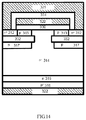
- FIG. 14 shows forming of the collector electrode ( 322 ).
- n-type channel device As an example. However, in the description below, it should be understood that the present invention is also applicable to a p-type channel device.
- a heavily doped n-type region is marked with n +
- a heavily doped p-type region is marked with p + .
- a heavily doped region generally has a doping concentration ranging from 1 ⁇ 10 19 cm ⁇ 3 to 1 ⁇ 10 21 cm ⁇ 3 .
- a lightly doped n-type region is marked with n ⁇
- a lightly doped p-type region is marked with p ⁇ .
- a lightly doped region generally has a doping concentration ranging from 1 ⁇ 10 13 cm ⁇ 3 to 1 ⁇ 10 17 cm ⁇ 3 .
- FIG. 3 is a cross-sectional view of the present invention implemented by using an IGBT device 300 .
- FIG. 4 is a top view of the IGBT device 300 .
- the device 300 includes: a collector electrode ( 322 ) located at the bottom; a p + collector region ( 316 ) located on top of the collector electrode ( 322 ); an n-type buffer region ( 315 ) located on top of the p + collector region ( 316 ); an n ⁇ drift region ( 314 ) located on top of the n-type buffer region ( 315 ); a p-type floating region ( 317 ), where the floating region is partially surrounded by the upper surface of the n ⁇ drift region ( 314 ); A buried oxide ( 332 ) located on top of the p-type floating region ( 317 ); an ultra-thin p-type base region ( 313 ) located on top of the buried oxide ( 332 ); a p + contact region ( 311 ) adjacent to the p
- the device 300 is a planar IGBT.
- V GE gate-emitter voltage
- the p-base ( 313 )/n ⁇ drift ( 314 ) junction can block the current from flowing from the collector electrode ( 322 ) to the emitter electrode ( 321 ). This keeps the device 300 at off-state.
- V CE collector-emitter voltage
- the p-type floating region ( 317 ) can protect the p-type base region ( 313 ) from being affected by the high electric field in the n ⁇ drift region ( 314 ).
- the ultra-thin p-type base region ( 313 ) is completely converted into an n + inversion layer.
- the n + inversion layer can conduct electrons from the n + emitter region ( 312 ) to the n ⁇ drift region ( 314 ), and therefore, the device is at an on-state.
- the concentration of electron-hole plasma near the n ⁇ inversion layer can be as high as the concentration of electron-hole plasma in a p-i-n diode. Therefore, the device 300 can implement the theoretically lowest on-state voltage drop.
- a negative V GE for example, ⁇ 15 V
- holes can be injected from the p + collector region ( 316 ) at the on-state of the device 300 , which is the same as the case in the device 100 .
- a doping concentration ranging from 1 ⁇ 10 18 cm ⁇ 3 to 1 ⁇ 10 21 cm ⁇ 3 and a depth ranging from 0.1 ⁇ m to 1 ⁇ m are preferable for the p + collector region ( 316 ).
- the doping concentration and the length of the n ⁇ drift region ( 314 ) depend on the rated voltage of the device 300 .
- An IGBT generally has a rated voltage ranging from 400 V to 6000 V. Based on the range, the doping concentration of the n ⁇ drift region ( 314 ) ranges from 1 ⁇ 10 12 cm ⁇ 3 to 1 ⁇ 10 15 cm ⁇ 3 , and the length of the n ⁇ drift region ( 314 ) ranges from 30 ⁇ m to 400 ⁇ m.
- the p-type floating region ( 317 ) should effectively protect the p-type base region ( 313 ) from the electric field in the n ⁇ drift region ( 314 ).
- the doping concentration of the p-type floating region ( 317 ) should be at least ten times greater than the doping concentration of the n ⁇ drift region ( 314 ), so as to avoid depletion in the off-state.
- the p-type floating region ( 317 ) should have a small depth, so that at the on-state, there is a wide current path in the n ⁇ drift region ( 314 ) near the p-type floating region ( 317 ).
- the depth of the p-type floating region ( 317 ) ranges from 0.3 ⁇ m to 3 ⁇ m.
- the n-type buffer region ( 315 ) should stop the expansion of the depletion region.
- the doping concentration of the n-type buffer region ( 315 ) should be greater than the doping concentration of the n ⁇ drift region ( 314 ). Because the off-state voltage is sustained mainly by the depleted n ⁇ drift region ( 314 ), the length of the n-type buffer region ( 315 ) can be much shorter than the length of the n ⁇ drift region ( 314 ).
- the function of the buried oxide ( 332 ) is electrically separating the p-type floating region ( 317 ) from the p-type base region ( 313 ). Therefore, thin buried oxide ( 332 ) is preferable, so as to reduce processing time and cost during manufacturing.
- the thickness of the buried oxide ( 332 ) ranges from 20 nm to 200 nm.
- the buried oxide ( 332 ) should have a width greater than widths of the p-type base region ( 313 ), the p + contact region ( 311 ), and the n + emitter region ( 312 ).
- neighboring cells should share the buried oxide ( 332 ), the p + contact region ( 311 ), and the n + emitter region ( 312 ).
- the buried oxide ( 332 ) is completely surrounded by semiconductor regions composed of the p-type floating region ( 317 ), the n ⁇ drift region ( 314 ), the p-type base region ( 313 ), the p + contact region ( 311 ) and the n + emitter region ( 312 ).
- the p-type base region ( 313 ) needs to be completely converted to an n + inversion layer.
- the feature can be implemented only by using an ultra-thin silicon layer and a proper doping concentration.
- An inversion layer generally has a thickness of approximately 10 nm.
- the thickness of the p-type base region ( 313 ) ranges from 5 nm to 20 nm, and the doping concentration of the p-type base region ( 313 ) is determined according to the threshold voltage requirement.
- the p + contact region ( 311 ) should connect the accumulated p-type base region ( 313 ) to the emitter electrode ( 321 ). Therefore, the p + contact region ( 311 ) should be heavily doped, to provide low parasitic resistance.
- the n + emitter region ( 312 ) should provide electrons to the channel, and the on-state current should flow though the n + emitter region ( 312 ) to reach the emitter electrode ( 321 ). Therefore, the n + emitter region ( 312 ) should be heavily doped, to provide low parasitic resistance.
- the width of the p + contact region ( 311 ) and the width of the n + emitter region ( 312 ) are not necessarily the same.
- a required saturation current should be provided. For example, in the state-of-the-art IGBTs, the saturation current is approximately 500 A/cm 2 .
- the p + contact region ( 311 ) should be capable of conducting a hole current that is large enough. Therefore, by means of design on the width of the p + contact region ( 311 ), a hole conducting area that is large enough should be provided, so as to safely switch off the device.
- FIG. 5 to FIG. 14 show a method for manufacturing the device 300 as shown in FIG. 3 and FIG. 4 .
- FIG. 5 shows forming of a mask oxide layer ( 333 ) on the surface of an initial wafer.
- the initial wafer is a lightly doped n-type substrate wafer.
- the doping concentration of the wafer depends on the rated voltage of the device 300 . Generally, the doping concentration of the n-type substrate wafer ranges from 1 ⁇ 10 12 cm ⁇ 3 to 1 ⁇ 10 15 cm ⁇ 3 .
- An intermediate product, that is, the mask oxide ( 333 ) is formed by depositing or thermally growing a silicon dioxide layer and then patterning the silicon dioxide layer.
- FIG. 6 shows forming of the buried oxide ( 332 ).
- the buried oxide ( 332 ) is made from silicon dioxide.
- the buried oxide is formed by using a method generally referred to as SIMOX, that is, separation with implanted oxygen.
- oxygen ions are injected by using the patterned oxide ( 333 ) as a hard mask.
- the wafer is annealed at a high temperature (for example, 1300° C.).
- a high temperature for example, 1300° C.
- a high temperature for example, 1300° C.
- FIG. 7 shows forming of the p-type base region ( 313 ) and the p-type floating region ( 317 ).
- photolithography is performed to define an implantation region.
- boron implantation is performed by using the patterned photoresist as a mask.
- implantation is performed once for forming the p-type base region ( 313 ) and the p-type floating region ( 317 ).
- implantation is performed multiple times for forming the p-type base region ( 313 ) and the p-type floating region ( 317 ), so as to meet different requirements on the concentrations and depths of the two regions.
- the photoresist is removed.
- annealing is performed to activate the dopant.
- the annealing is rapid thermal annealing, so as to minimize diffusion of the dopant.
- FIG. 8 shows forming of the gate stack.
- the gate dielectric ( 330 ) is formed.
- the gate dielectric ( 330 ) is formed by oxidizing the surface of silicon. This can further reduce the thickness of the p-type base region ( 313 ).
- the gate dielectric ( 330 ) is formed by oxidizing the surface of silicon and then depositing a dielectric having a high dielectric constant. This can reduce thermal diffusion in the p-type base region ( 313 ), and therefore, impurity concentration distribution is more controllable.
- polysilicon is deposited and patterned to form the gate electrode ( 320 ).
- FIG. 9 shows forming of the p + contact region ( 311 ) and n + emitter region ( 312 ).
- photolithography is performed for the p + contact region ( 311 ).
- boron implantation is performed by using the patterned photoresist as a mask.
- the photoresist is removed.
- annealing is performed to activate the boron ions, so as to form the p + contact region ( 311 ).
- photolithography is performed for the n + emitter region ( 312 ).
- arsenic or phosphorous implantation is performed by using the patterned photoresist as a mask.
- the photoresist is removed.
- annealing is performed to activate the arsenic ions or phosphorous ions, so as to form the n + emitter region ( 312 ).
- the foregoing annealing steps can be combined, so as to activate boron ions and arsenic/phosphorous ions ions at the same time.
- FIG. 10 shows forming of the ILD ( 331 ).
- the ILD ( 331 ) is silicon dioxide.
- the ILD ( 331 ) is deposited by means of chemical vapor deposition.
- FIG. 11 shows forming of a contact hole ( 340 ).
- the contact hole ( 340 ) is formed by patterning the ILD ( 331 ).
- FIG. 12 shows forming of the emitter electrode ( 321 ) and n ⁇ drift region ( 314 ).
- metal is deposited and the contact hole ( 340 ) is filled with the metal.
- the metal is patterned, so as to form the emitter electrode ( 321 ).
- the substrate wafer is thinned from the back surface, so as to form the n ⁇ drift region ( 314 ).
- the thinning process is first performing mechanical grinding, and then performing chemical etching.
- FIG. 13 shows forming of the n-type buffer region ( 315 ) and p + collector region ( 316 ).
- phosphorous ions are implanted into the back surface of the wafer.
- annealing is performed to activate the implanted phosphorous ions, thereby forming the n-type buffer region ( 315 ).
- boron ions are implanted into the back surface of the wafer.
- annealing is performed to activate the implanted boron ions, thereby forming the p + collector region ( 316 ).
- annealing is usually performed on the n-type buffer region ( 315 ) and the p + collector region ( 316 ) at a low temperature (for example, 480° C.). However, laser annealing can be performed at a high temperature (for example, 1000° C.). In addition, annealing can be performed once to activate the n-type buffer region ( 315 ) and the p + collector region ( 316 ) at the same time.
- FIG. 14 shows forming of the collector electrode ( 322 ).
- the collector electrode ( 322 ) is formed by depositing a metal layer on the back surface of the wafer. After the metal is deposited, preferably, alloying is performed, so as to reduce contact resistance between the collector electrode ( 322 ) and the p + collector region ( 316 ).
- the order of the steps above can be adjusted according to the manufacturing capability. For example, if ions in the n-type buffer region ( 315 ) and the p + collector region ( 316 ) need to be activated completely without using an expensive laser annealing system, the contact hole ( 340 ) and the emitter electrode ( 321 ) can be formed after the n-type buffer region ( 315 ) and the p + collector region ( 316 ) are formed. However, if the contact hole ( 340 ) and the emitter electrode ( 321 ) are formed after the wafer is thinned, a photolithography system applicable to thin wafers is needed.
Landscapes
- Electrodes Of Semiconductors (AREA)
- Thin Film Transistor (AREA)
Abstract
Description
Claims (18)
Applications Claiming Priority (1)
| Application Number | Priority Date | Filing Date | Title |
|---|---|---|---|
| PCT/CN2016/087583 WO2018000223A1 (en) | 2016-06-29 | 2016-06-29 | Insulated gate bipolar transistor structure and manufacturing method therefor |
Publications (2)
| Publication Number | Publication Date |
|---|---|
| US20180226500A1 US20180226500A1 (en) | 2018-08-09 |
| US10692995B2 true US10692995B2 (en) | 2020-06-23 |
Family
ID=60785064
Family Applications (1)
| Application Number | Title | Priority Date | Filing Date |
|---|---|---|---|
| US15/571,230 Active 2036-10-29 US10692995B2 (en) | 2016-06-29 | 2016-06-29 | Insulated-gate bipolar transistor structure and method for manufacturing the same |
Country Status (2)
| Country | Link |
|---|---|
| US (1) | US10692995B2 (en) |
| WO (1) | WO2018000223A1 (en) |
Families Citing this family (4)
| Publication number | Priority date | Publication date | Assignee | Title |
|---|---|---|---|---|
| CN110690278B (en) * | 2019-10-22 | 2023-02-03 | 上海睿驱微电子科技有限公司 | A kind of insulated gate bipolar transistor and its preparation method |
| CN112864234B (en) * | 2019-11-27 | 2022-04-15 | 苏州东微半导体股份有限公司 | IGBT power devices |
| CN113066867B (en) * | 2021-03-15 | 2022-09-09 | 无锡新洁能股份有限公司 | High reliability silicon carbide MOSFET device and process method thereof |
| CN113270492A (en) * | 2021-05-13 | 2021-08-17 | 重庆邮电大学 | Trench type GaN insulated gate bipolar transistor |
Citations (7)
| Publication number | Priority date | Publication date | Assignee | Title |
|---|---|---|---|---|
| JP2005135979A (en) | 2003-10-28 | 2005-05-26 | Shindengen Electric Mfg Co Ltd | Insulated gate-type bipolar transistor and manufacturing method therefor |
| US20090050932A1 (en) * | 2005-03-03 | 2009-02-26 | Fuji Electric Holdings Co., Ltd. | Semiconductor device and the method of manufacturing the same |
| CN101901830A (en) | 2009-11-09 | 2010-12-01 | 苏州博创集成电路设计有限公司 | Forward and reverse conduction lateral insulated gate bipolar transistor of silicon on insulator |
| US20110204413A1 (en) * | 2010-02-25 | 2011-08-25 | Daisuke Arai | Semiconductor device and manufacturing method of the same |
| CN102254942A (en) | 2011-07-27 | 2011-11-23 | 江苏物联网研究发展中心 | Novel Insulated Gate Bipolar Transistor (IGBT) with stepped gate structure and manufacturing method thereof |
| CN104810282A (en) | 2014-01-26 | 2015-07-29 | 国家电网公司 | Method for manufacturing N-channel IGBT device by using N-type silicon carbide substrate |
| CN105390536A (en) | 2015-09-30 | 2016-03-09 | 深圳市可易亚半导体科技有限公司 | Insulated gate bipolar transistor and manufacturing method thereof |
-
2016
- 2016-06-29 WO PCT/CN2016/087583 patent/WO2018000223A1/en not_active Ceased
- 2016-06-29 US US15/571,230 patent/US10692995B2/en active Active
Patent Citations (8)
| Publication number | Priority date | Publication date | Assignee | Title |
|---|---|---|---|---|
| JP2005135979A (en) | 2003-10-28 | 2005-05-26 | Shindengen Electric Mfg Co Ltd | Insulated gate-type bipolar transistor and manufacturing method therefor |
| US20090050932A1 (en) * | 2005-03-03 | 2009-02-26 | Fuji Electric Holdings Co., Ltd. | Semiconductor device and the method of manufacturing the same |
| CN101901830A (en) | 2009-11-09 | 2010-12-01 | 苏州博创集成电路设计有限公司 | Forward and reverse conduction lateral insulated gate bipolar transistor of silicon on insulator |
| US20110204413A1 (en) * | 2010-02-25 | 2011-08-25 | Daisuke Arai | Semiconductor device and manufacturing method of the same |
| CN102804384A (en) | 2010-02-25 | 2012-11-28 | 瑞萨电子株式会社 | Semiconductor device and manufacturing method thereof |
| CN102254942A (en) | 2011-07-27 | 2011-11-23 | 江苏物联网研究发展中心 | Novel Insulated Gate Bipolar Transistor (IGBT) with stepped gate structure and manufacturing method thereof |
| CN104810282A (en) | 2014-01-26 | 2015-07-29 | 国家电网公司 | Method for manufacturing N-channel IGBT device by using N-type silicon carbide substrate |
| CN105390536A (en) | 2015-09-30 | 2016-03-09 | 深圳市可易亚半导体科技有限公司 | Insulated gate bipolar transistor and manufacturing method thereof |
Non-Patent Citations (1)
| Title |
|---|
| International Search Report and Written Opinion of PCT/CN2016/087583, dated Mar. 2, 2017, 11 pages. |
Also Published As
| Publication number | Publication date |
|---|---|
| US20180226500A1 (en) | 2018-08-09 |
| WO2018000223A1 (en) | 2018-01-04 |
Similar Documents
| Publication | Publication Date | Title |
|---|---|---|
| KR100886883B1 (en) | Method for fabricating forward and reverse blocking devices | |
| US9209242B2 (en) | Semiconductor device with an edge termination structure having a closed vertical trench | |
| US10593788B2 (en) | Reverse-conducting insulated-gate bipolar transistor structure and corresponding fabrication method thereof | |
| US11081575B2 (en) | Insulated gate bipolar transistor device and method for manufacturing the same | |
| KR101955055B1 (en) | Power semiconductor device and method of fabricating the same | |
| CN106997899B (en) | A kind of IGBT device and preparation method thereof | |
| CN112930601A (en) | Insulated gate power semiconductor device and method of manufacturing the same | |
| CN107634094B (en) | Insulated gate bipolar transistor structure and manufacturing method thereof | |
| US7355263B2 (en) | Semiconductor device and manufacturing method thereof | |
| EP3474330B1 (en) | Lateral insulated-gate bipolar transistor and manufacturing method therefor | |
| KR102088181B1 (en) | A semiconductor transistor and method for forming the semiconductor transistor | |
| CN110518058A (en) | A kind of lateral trench type insulated gate bipolar transistor and preparation method thereof | |
| US10692995B2 (en) | Insulated-gate bipolar transistor structure and method for manufacturing the same | |
| CN107534053A (en) | Semiconductor device and manufacturing method thereof | |
| JP4096722B2 (en) | Manufacturing method of semiconductor device | |
| US9245986B2 (en) | Power semiconductor device and method of manufacturing the same | |
| CN107833915A (en) | Semiconductor devices | |
| CN110473905A (en) | A kind of separate gate TIGBT and preparation method thereof with automatic biasing PMOS | |
| JP5114832B2 (en) | Semiconductor device and manufacturing method thereof | |
| JP4904635B2 (en) | Semiconductor device and manufacturing method thereof | |
| JP5028749B2 (en) | Manufacturing method of semiconductor device | |
| US20160284826A1 (en) | Bipolar non-punch-through power semiconductor device | |
| JPH10335630A (en) | Semiconductor device and manufacturing method thereof | |
| CN105762077A (en) | Manufacturing method of insulated gate bipolar transistor | |
| CN106098761A (en) | Insulated gate bipolar transistor structure and manufacturing method thereof |
Legal Events
| Date | Code | Title | Description |
|---|---|---|---|
| AS | Assignment |
Owner name: WONG, KA KIT, HONG KONG Free format text: ASSIGNMENT OF ASSIGNORS INTEREST;ASSIGNORS:ZHOU, XIANDA;WONG, KA KIT;SIN, KIN ON JOHNNY;REEL/FRAME:044011/0095 Effective date: 20171018 |
|
| FEPP | Fee payment procedure |
Free format text: ENTITY STATUS SET TO UNDISCOUNTED (ORIGINAL EVENT CODE: BIG.); ENTITY STATUS OF PATENT OWNER: SMALL ENTITY |
|
| FEPP | Fee payment procedure |
Free format text: ENTITY STATUS SET TO SMALL (ORIGINAL EVENT CODE: SMAL); ENTITY STATUS OF PATENT OWNER: SMALL ENTITY |
|
| STPP | Information on status: patent application and granting procedure in general |
Free format text: APPLICATION DISPATCHED FROM PREEXAM, NOT YET DOCKETED |
|
| STPP | Information on status: patent application and granting procedure in general |
Free format text: DOCKETED NEW CASE - READY FOR EXAMINATION |
|
| STPP | Information on status: patent application and granting procedure in general |
Free format text: NON FINAL ACTION MAILED |
|
| STPP | Information on status: patent application and granting procedure in general |
Free format text: NON FINAL ACTION MAILED |
|
| STPP | Information on status: patent application and granting procedure in general |
Free format text: EX PARTE QUAYLE ACTION MAILED |
|
| STPP | Information on status: patent application and granting procedure in general |
Free format text: RESPONSE TO EX PARTE QUAYLE ACTION ENTERED AND FORWARDED TO EXAMINER |
|
| STPP | Information on status: patent application and granting procedure in general |
Free format text: NOTICE OF ALLOWANCE MAILED -- APPLICATION RECEIVED IN OFFICE OF PUBLICATIONS |
|
| STPP | Information on status: patent application and granting procedure in general |
Free format text: PUBLICATIONS -- ISSUE FEE PAYMENT VERIFIED |
|
| STCF | Information on status: patent grant |
Free format text: PATENTED CASE |
|
| AS | Assignment |
Owner name: JSAB TECHNOLOGIES (SHENZHEN) LIMITED, CHINA Free format text: ASSIGNMENT OF ASSIGNORS INTEREST;ASSIGNOR:WONG, KA KIT;REEL/FRAME:058165/0245 Effective date: 20210923 |
|
| MAFP | Maintenance fee payment |
Free format text: PAYMENT OF MAINTENANCE FEE, 4TH YR, SMALL ENTITY (ORIGINAL EVENT CODE: M2551); ENTITY STATUS OF PATENT OWNER: SMALL ENTITY Year of fee payment: 4 |