US10692890B2 - Display device, stacked substrate including the same, and method for manufacturing the display device - Google Patents
Display device, stacked substrate including the same, and method for manufacturing the display device Download PDFInfo
- Publication number
- US10692890B2 US10692890B2 US16/273,554 US201916273554A US10692890B2 US 10692890 B2 US10692890 B2 US 10692890B2 US 201916273554 A US201916273554 A US 201916273554A US 10692890 B2 US10692890 B2 US 10692890B2
- Authority
- US
- United States
- Prior art keywords
- layer
- soluble
- cover layer
- forming
- carrier substrate
- Prior art date
- Legal status (The legal status is an assumption and is not a legal conclusion. Google has not performed a legal analysis and makes no representation as to the accuracy of the status listed.)
- Active
Links
Images


Classifications
-
- H—ELECTRICITY
- H10—SEMICONDUCTOR DEVICES; ELECTRIC SOLID-STATE DEVICES NOT OTHERWISE PROVIDED FOR
- H10K—ORGANIC ELECTRIC SOLID-STATE DEVICES
- H10K71/00—Manufacture or treatment specially adapted for the organic devices covered by this subclass
-
- H—ELECTRICITY
- H10—SEMICONDUCTOR DEVICES; ELECTRIC SOLID-STATE DEVICES NOT OTHERWISE PROVIDED FOR
- H10D—INORGANIC ELECTRIC SEMICONDUCTOR DEVICES
- H10D86/00—Integrated devices formed in or on insulating or conducting substrates, e.g. formed in silicon-on-insulator [SOI] substrates or on stainless steel or glass substrates
- H10D86/01—Manufacture or treatment
- H10D86/021—Manufacture or treatment of multiple TFTs
- H10D86/0214—Manufacture or treatment of multiple TFTs using temporary substrates
-
- H01L27/1218—
-
- H01L25/048—
-
- H01L27/1266—
-
- H01L27/3276—
-
- H01L51/003—
-
- H01L51/0097—
-
- H01L51/5237—
-
- H01L51/56—
-
- H—ELECTRICITY
- H10—SEMICONDUCTOR DEVICES; ELECTRIC SOLID-STATE DEVICES NOT OTHERWISE PROVIDED FOR
- H10D—INORGANIC ELECTRIC SEMICONDUCTOR DEVICES
- H10D86/00—Integrated devices formed in or on insulating or conducting substrates, e.g. formed in silicon-on-insulator [SOI] substrates or on stainless steel or glass substrates
- H10D86/40—Integrated devices formed in or on insulating or conducting substrates, e.g. formed in silicon-on-insulator [SOI] substrates or on stainless steel or glass substrates characterised by multiple TFTs
- H10D86/411—Integrated devices formed in or on insulating or conducting substrates, e.g. formed in silicon-on-insulator [SOI] substrates or on stainless steel or glass substrates characterised by multiple TFTs characterised by materials, geometry or structure of the substrates
-
- H—ELECTRICITY
- H10—SEMICONDUCTOR DEVICES; ELECTRIC SOLID-STATE DEVICES NOT OTHERWISE PROVIDED FOR
- H10D—INORGANIC ELECTRIC SEMICONDUCTOR DEVICES
- H10D86/00—Integrated devices formed in or on insulating or conducting substrates, e.g. formed in silicon-on-insulator [SOI] substrates or on stainless steel or glass substrates
- H10D86/40—Integrated devices formed in or on insulating or conducting substrates, e.g. formed in silicon-on-insulator [SOI] substrates or on stainless steel or glass substrates characterised by multiple TFTs
- H10D86/60—Integrated devices formed in or on insulating or conducting substrates, e.g. formed in silicon-on-insulator [SOI] substrates or on stainless steel or glass substrates characterised by multiple TFTs wherein the TFTs are in active matrices
-
- H—ELECTRICITY
- H10—SEMICONDUCTOR DEVICES; ELECTRIC SOLID-STATE DEVICES NOT OTHERWISE PROVIDED FOR
- H10K—ORGANIC ELECTRIC SOLID-STATE DEVICES
- H10K50/00—Organic light-emitting devices
- H10K50/80—Constructional details
- H10K50/84—Passivation; Containers; Encapsulations
-
- H—ELECTRICITY
- H10—SEMICONDUCTOR DEVICES; ELECTRIC SOLID-STATE DEVICES NOT OTHERWISE PROVIDED FOR
- H10K—ORGANIC ELECTRIC SOLID-STATE DEVICES
- H10K50/00—Organic light-emitting devices
- H10K50/80—Constructional details
- H10K50/84—Passivation; Containers; Encapsulations
- H10K50/844—Encapsulations
-
- H—ELECTRICITY
- H10—SEMICONDUCTOR DEVICES; ELECTRIC SOLID-STATE DEVICES NOT OTHERWISE PROVIDED FOR
- H10K—ORGANIC ELECTRIC SOLID-STATE DEVICES
- H10K59/00—Integrated devices, or assemblies of multiple devices, comprising at least one organic light-emitting element covered by group H10K50/00
- H10K59/10—OLED displays
- H10K59/12—Active-matrix OLED [AMOLED] displays
- H10K59/1201—Manufacture or treatment
-
- H—ELECTRICITY
- H10—SEMICONDUCTOR DEVICES; ELECTRIC SOLID-STATE DEVICES NOT OTHERWISE PROVIDED FOR
- H10K—ORGANIC ELECTRIC SOLID-STATE DEVICES
- H10K59/00—Integrated devices, or assemblies of multiple devices, comprising at least one organic light-emitting element covered by group H10K50/00
- H10K59/10—OLED displays
- H10K59/12—Active-matrix OLED [AMOLED] displays
- H10K59/131—Interconnections, e.g. wiring lines or terminals
-
- H—ELECTRICITY
- H10—SEMICONDUCTOR DEVICES; ELECTRIC SOLID-STATE DEVICES NOT OTHERWISE PROVIDED FOR
- H10K—ORGANIC ELECTRIC SOLID-STATE DEVICES
- H10K59/00—Integrated devices, or assemblies of multiple devices, comprising at least one organic light-emitting element covered by group H10K50/00
- H10K59/90—Assemblies of multiple devices comprising at least one organic light-emitting element
-
- H—ELECTRICITY
- H10—SEMICONDUCTOR DEVICES; ELECTRIC SOLID-STATE DEVICES NOT OTHERWISE PROVIDED FOR
- H10K—ORGANIC ELECTRIC SOLID-STATE DEVICES
- H10K71/00—Manufacture or treatment specially adapted for the organic devices covered by this subclass
- H10K71/10—Deposition of organic active material
- H10K71/16—Deposition of organic active material using physical vapour deposition [PVD], e.g. vacuum deposition or sputtering
-
- H—ELECTRICITY
- H10—SEMICONDUCTOR DEVICES; ELECTRIC SOLID-STATE DEVICES NOT OTHERWISE PROVIDED FOR
- H10K—ORGANIC ELECTRIC SOLID-STATE DEVICES
- H10K71/00—Manufacture or treatment specially adapted for the organic devices covered by this subclass
- H10K71/20—Changing the shape of the active layer in the devices, e.g. patterning
- H10K71/231—Changing the shape of the active layer in the devices, e.g. patterning by etching of existing layers
-
- H—ELECTRICITY
- H10—SEMICONDUCTOR DEVICES; ELECTRIC SOLID-STATE DEVICES NOT OTHERWISE PROVIDED FOR
- H10K—ORGANIC ELECTRIC SOLID-STATE DEVICES
- H10K71/00—Manufacture or treatment specially adapted for the organic devices covered by this subclass
- H10K71/311—Purifying organic semiconductor materials
-
- H—ELECTRICITY
- H10—SEMICONDUCTOR DEVICES; ELECTRIC SOLID-STATE DEVICES NOT OTHERWISE PROVIDED FOR
- H10K—ORGANIC ELECTRIC SOLID-STATE DEVICES
- H10K71/00—Manufacture or treatment specially adapted for the organic devices covered by this subclass
- H10K71/80—Manufacture or treatment specially adapted for the organic devices covered by this subclass using temporary substrates
-
- H—ELECTRICITY
- H10—SEMICONDUCTOR DEVICES; ELECTRIC SOLID-STATE DEVICES NOT OTHERWISE PROVIDED FOR
- H10K—ORGANIC ELECTRIC SOLID-STATE DEVICES
- H10K71/00—Manufacture or treatment specially adapted for the organic devices covered by this subclass
- H10K71/851—Division of substrate
-
- H01L2251/5338—
-
- H01L2251/566—
-
- H01L27/3244—
-
- H—ELECTRICITY
- H10—SEMICONDUCTOR DEVICES; ELECTRIC SOLID-STATE DEVICES NOT OTHERWISE PROVIDED FOR
- H10K—ORGANIC ELECTRIC SOLID-STATE DEVICES
- H10K2102/00—Constructional details relating to the organic devices covered by this subclass
- H10K2102/301—Details of OLEDs
- H10K2102/311—Flexible OLED
-
- H—ELECTRICITY
- H10—SEMICONDUCTOR DEVICES; ELECTRIC SOLID-STATE DEVICES NOT OTHERWISE PROVIDED FOR
- H10K—ORGANIC ELECTRIC SOLID-STATE DEVICES
- H10K59/00—Integrated devices, or assemblies of multiple devices, comprising at least one organic light-emitting element covered by group H10K50/00
- H10K59/10—OLED displays
- H10K59/12—Active-matrix OLED [AMOLED] displays
-
- H—ELECTRICITY
- H10—SEMICONDUCTOR DEVICES; ELECTRIC SOLID-STATE DEVICES NOT OTHERWISE PROVIDED FOR
- H10K—ORGANIC ELECTRIC SOLID-STATE DEVICES
- H10K59/00—Integrated devices, or assemblies of multiple devices, comprising at least one organic light-emitting element covered by group H10K50/00
- H10K59/80—Constructional details
- H10K59/87—Passivation; Containers; Encapsulations
-
- H—ELECTRICITY
- H10—SEMICONDUCTOR DEVICES; ELECTRIC SOLID-STATE DEVICES NOT OTHERWISE PROVIDED FOR
- H10K—ORGANIC ELECTRIC SOLID-STATE DEVICES
- H10K77/00—Constructional details of devices covered by this subclass and not covered by groups H10K10/80, H10K30/80, H10K50/80 or H10K59/80
- H10K77/10—Substrates, e.g. flexible substrates
- H10K77/111—Flexible substrates
-
- Y—GENERAL TAGGING OF NEW TECHNOLOGICAL DEVELOPMENTS; GENERAL TAGGING OF CROSS-SECTIONAL TECHNOLOGIES SPANNING OVER SEVERAL SECTIONS OF THE IPC; TECHNICAL SUBJECTS COVERED BY FORMER USPC CROSS-REFERENCE ART COLLECTIONS [XRACs] AND DIGESTS
- Y02—TECHNOLOGIES OR APPLICATIONS FOR MITIGATION OR ADAPTATION AGAINST CLIMATE CHANGE
- Y02E—REDUCTION OF GREENHOUSE GAS [GHG] EMISSIONS, RELATED TO ENERGY GENERATION, TRANSMISSION OR DISTRIBUTION
- Y02E10/00—Energy generation through renewable energy sources
- Y02E10/50—Photovoltaic [PV] energy
- Y02E10/549—Organic PV cells
-
- Y—GENERAL TAGGING OF NEW TECHNOLOGICAL DEVELOPMENTS; GENERAL TAGGING OF CROSS-SECTIONAL TECHNOLOGIES SPANNING OVER SEVERAL SECTIONS OF THE IPC; TECHNICAL SUBJECTS COVERED BY FORMER USPC CROSS-REFERENCE ART COLLECTIONS [XRACs] AND DIGESTS
- Y02—TECHNOLOGIES OR APPLICATIONS FOR MITIGATION OR ADAPTATION AGAINST CLIMATE CHANGE
- Y02P—CLIMATE CHANGE MITIGATION TECHNOLOGIES IN THE PRODUCTION OR PROCESSING OF GOODS
- Y02P70/00—Climate change mitigation technologies in the production process for final industrial or consumer products
- Y02P70/50—Manufacturing or production processes characterised by the final manufactured product
Definitions
- Exemplary embodiments of the present invention relate to a display device, and more particularly, to a stacked substrate including the same, and a method for manufacturing the display device.
- Display panels may display images to provide a user with information.
- the display panels may include a base substrate and a display element disposed on the base substrate.
- the display device may generate an image according to an electrical signal.
- Display panels may include a base substrate having flexibility, and thus a flexible display panel may be provided.
- the flexible display panel may be provided in such a manner in which a flexible base substrate is provided on a carrier substrate, and a display element may be disposed on the base substrate through depositing and patterning, and then the base substrate may be separated from the carrier substrate.
- an irradiating process using a laser may be used.
- An exemplary embodiment of the present invention provides a stacked substrate, which is separated from a carrier substrate while omitting a separation process such as laser irradiation, and a method for manufacturing a display device.
- An exemplary embodiment of the present invention provides a display device including a base substrate that is separated from a carrier substrate in which an occurrence of damage to the display device is reduced or eliminated. For example, an occurrence of heat damage during a heat treatment process, such as a laser irradiation process, may be eliminated. Additionally, a manufacturing cost of the display device may be reduced.
- An exemplary embodiment of the present invention provides a method for manufacturing a display device including providing a carrier substrate and forming a soluble layer on the carrier substrate.
- the soluble layer includes a material that dissolves in a washing solution.
- the method includes forming a cover layer on a top surface of the soluble layer and a side surface of the soluble layer.
- the method includes forming a display panel on the cover layer.
- the display panel includes a base layer.
- the method includes removing a portion of the cover layer from the side surface of the soluble layer to form a remaining part.
- the method includes providing the washing solution to the soluble layer to remove the soluble layer.
- the method includes separating the display panel and the remaining part from the carrier substrate.
- the soluble layer may include MoO 3
- the cover layer and the remaining part may include MoO 2 .
- the soluble layer and the cover layer may be formed using a sputtering process.
- the forming of the remaining part may be performed using a wet etching process in which an etching solution is provided to the cover layer to remove the portion of the cover layer.
- a plurality of soluble layers may be formed in the forming of the soluble layer.
- a plurality of display panels may be formed, and the display panels may be disposed on the soluble layers in a one-to-one corresponding manner.
- the method may include cutting boundaries between the display panels to separate the display panels from each other.
- a portion of the cover layer may be removed to form a plurality of remaining parts.
- the method may include removing a portion of the cover layer to form a plurality of remaining parts, in the forming of the remaining part.
- the method may include dissolving the plurality of soluble layers to separate the display panels and the remaining parts from the carrier substrate.
- the method may include cutting boundaries between the display panels to separate the display panels from each other.
- through-holes may be defined in a region of the carrier substrate, which does not overlap the soluble layers on a plane.
- An etching solution for removing the portion of the cover layer may pass through the through-holes and may be supplied to the cover layer disposed between the soluble layers.
- the method may include defining through-holes in the carrier substrate.
- the method may include forming a lower cover layer on a top surface of the carrier substrate.
- the lower cover layer may be disposed between the carrier substrate and the soluble layer such that top and side surfaces of the soluble layer are covered by the cover layer and a bottom surface of the soluble layer is covered by the lower cover layer.
- the cover layer and the lower cover layer may include a same material as each other. In the removing of the portion of the cover layer to form the remaining part, a portion of the lower cover layer, which overlaps the through-holes on a plane, may be removed.
- the washing solution in the removing of the soluble layer, may be supplied along the side surface of the soluble layer, the through-holes, and the removed portion of the lower cover layer.
- the base layer may include a central region and a peripheral region adjacent to the central region. The remaining part may overlap the central region and need not overlap the peripheral region, on a plane.
- the forming of the display panel may include forming the base layer on the cover layer using a coating process.
- a circuit layer may be formed on the base layer.
- a light emitting element layer may be formed on the circuit layer.
- a thin film encapsulation layer may be formed on the light emitting element layer.
- a stacked substrate includes a carrier substrate and a soluble layer disposed on the carrier substrate.
- a cover layer is disposed on a top surface of the soluble layer and a side surface of the soluble layer.
- a display panel includes a base layer which is disposed on the cover layer and includes a central region and a peripheral region adjacent to the central region. The soluble layer overlaps the central region and does not overlap the peripheral region, on a plane.
- a plurality of through-holes may be defined in the carrier substrate.
- the stacked substrate may include a lower cover layer which covers the plurality of through-holes and is disposed between the carrier substrate and the soluble layer.
- the soluble layer and the display panel may be provided in plurality.
- the plurality of the soluble layers may be spaced apart from each other, and the cover layer may cover a top surface and a side surface of each of the soluble layers.
- a plurality of through-holes may be defined in a region of the carrier substrate, which does not overlap the soluble layers on plane.
- the soluble layer may include MoO 3
- the cover layer may include MoO 2 .
- a display device in an exemplary embodiment of the present invention, includes a display panel including a base layer which includes a central region and a peripheral region adjacent to the central region. A remaining part of a cover layer is disposed under the display panel, and overlaps the central region and does not overlap the peripheral region.
- the remaining part may include MoO 2 .
- FIG. 1 is a perspective view of a display device according to an exemplary embodiment of the present invention
- FIG. 2A is a cross-sectional view of the display device of FIG. 1 ;
- FIG. 2B is a rear view of the display device of FIG. 2A ;
- FIGS. 3A, 3B, 3C, 3D, 3E, 3F, 3G and 3H are cross-sectional views of a method for manufacturing a display device according to an exemplary embodiment of the present invention.
- FIGS. 4A, 4B, 4C, 4D, 4E, 4F, 4G and 4H are cross-sectional views of a method for manufacturing a display device according to an exemplary embodiment of the present invention.
- FIGS. 5A, 5B, 5C, 5D, 5E, 5F, 5G, 5H and 5I are cross-sectional views of a method for manufacturing a display device according to an exemplary embodiment of the present invention.
- FIGS. 6A, 6B, 6C, 6D, 6E, 6F, 6G, 6H and 6I are cross-sectional views of a method for manufacturing a display device according to an exemplary embodiment of the present invention.
- FIG. 7A is a plan view of a carrier substrate according to an exemplary embodiment of the present invention.
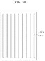
- FIG. 7B is a plan view of a carrier substrate according to an exemplary embodiment of the present invention.
- a component such as a layer, a film, a region, or a plate
- the component may be directly on the other component or intervening components may be present.
- FIG. 1 is a perspective view of a display device according to an exemplary embodiment of the present invention.
- a display device DD may display an image IM through a display surface IS.
- the display surface IS may be parallel to a surface defined by a first direction DR 1 and a second direction DR 2 crossing the first direction DR 1 .
- a display device may have a curved shape.
- the display device may be a bendable or foldable display device that is in a curved or bent state at some times and is in a substantially flat state at other times.
- the display device may be in a permanently folded, curved or bent state.
- the first direction DR 1 may be perpendicular to the second direction DR 2 .
- the first direction DR 1 and the second direction DR 2 may define a plane along which the display panel extends.
- a third direction DR 3 may be perpendicular to the first and second direction DR 1 and DR 2 .
- the third direction DR 3 may be orthogonal to a plane extending in the first and second direction DR 1 and DR 2 .
- a normal direction of the display surface IS for example, a thickness direction of the display device DD may extend in the third direction DR 3 .
- a front surface (e.g., a top surface) and a rear surface (e.g., a bottom surface) in each of the members may be spaced apart from each other in the third direction DR 3 .
- directions that are indicated as the first to third directions DR 1 , DR 2 , and DR 3 may have a relative concept and thus be changed to other directions.
- first to third directions may refer to the same reference symbols as the directions indicated by the first and third directions DR 1 , DR 2 , and DR 3 , respectively.
- the display device DD may be a mobile electronic device.
- the display device DD may be used in relatively large scale electronic devices such as a television, a monitor, an outdoor advertising board, as well as, in relatively small-to-medium scale electronic devices such as a personal computer, a laptop computer, a personal digital terminal, a vehicle navigation unit, a game console, a smart phone, a tablet, or a camera; however, exemplary embodiments of the present invention are not limited thereto, and thus other electronic devices may include the display device DD described herein.
- the display surface IS may include a display area DA on which the image IM is displayed and a non-display area NDA adjacent to the display area DA.
- the non-display area NDA an image might not be displayed.
- application icons are illustrated as one example of the image IM.
- the display area DA may have a tetragonal shape.
- the non-display area NDA may surround the display area DA.
- exemplary embodiments of the present invention are not limited thereto, and the shapes of the display area DA and the non-display area NDA may be relatively designed.
- the non-display area NDA need not be present on a front surface of the display device DD.
- the non-display area NDA may be positioned at a curved side surface of the display device DD that extends at an angle with respect to the first and second directions DR 1 and DR 2 .
- the non-display region NDA may be arranged at four sides of the display region DA in a plan view; however, exemplary embodiments of the present invention are not limited thereto.
- the non-display region NDA may be arranged at less than four sides (e.g., three sides) of the display region DA in a plan view.
- FIG. 2A is a cross-sectional view of the display device of FIG. 1 .
- FIG. 2B is a rear view of the display device of FIG. 2A .
- the display device DD may include a display panel DP, a sensing unit SU, and a remaining part CL- 1 .
- the display panel DP may be a light emitting-type display panel, but is not particularly limited thereto.
- the display panel DP may be an organic light emitting display panel or a quantum-dot light emitting display panel.
- a light emitting layer of the organic light emitting display panel may include an organic light emitting material.
- a light emitting layer of the quantum-dot light emitting display panel may include at least one of quantum dots and quantum rods.
- the display panel DP is described as an organic light emitting display panel below as an example; however, exemplary embodiments of the present invention are not limited thereto.
- the display panel DP may include a base layer BL, a circuit layer ML, a light emitting element layer EL, and a thin film encapsulation layer ECL.
- the base layer BL may include an insulation substrate.
- the base layer BL may have flexible characteristics.
- the base layer may be optically transparent.
- the base layer may be translucent.
- the base layer BL may be a stacked structure including a plastic substrate, an organic/inorganic composite material substrate, or a plurality of insulation layers.
- the base substrate BL may include at least one of polyimide, polycarbonate, polyester, or polyacrylate.
- the circuit layer ML may be disposed on the base layer BL.
- the circuit layer ML may include a plurality of insulation layers, a plurality of conductive layers, and a semiconductor layer.
- the plurality of conductive layers of the circuit layer ML may include signal lines and a control circuit of a pixel.
- the light emitting element layer EL may include, for example, an organic light emitting diode.
- exemplary embodiments of the present invention are not limited thereto, and the light emitting element layer EL may include inorganic light emitting diodes or organic-inorganic hybrid light emitting diodes (e.g., according to the types of the display panel DP).
- the thin film encapsulation layer ECL may seal the light emitting element layer EL.
- the thin film encapsulation layer ECL may include at least one insulation layer.
- the thin film encapsulation layer ECL according to an exemplary embodiment of the present invention may include at least one encapsulation-organic film and at least one encapsulation-inorganic film.
- the encapsulation-inorganic film may protect the light emitting element layer EL against moisture/oxygen, and the encapsulation-organic film may protect the light emitting element layer EL against impurities such as dust particles.
- the encapsulation-inorganic film may include, but is not particularly limited to, a silicon nitride layer, a silicon oxynitride layer, a silicon oxide layer, a titanium oxide layer, or an aluminum oxide layer.
- the encapsulation-organic film may include, but is not particularly limited to, an acrylic-based organic film.
- the sensing unit SU may be disposed on the thin film encapsulation layer ECL.
- the sensing unit SU may detect an external input, for example, by a capacitive method.
- an operation method of the sensing unit SU is not particularly limited to a particular method, and in an exemplary embodiment of the present invention, the sensing unit SU may detect an external input by a magnetic induction method or a pressure detection method.
- the sensing unit SU may be directly formed on the thin film encapsulation layer ECL.
- the sensing unit SU and the thin film encapsulation layer ECL may be formed through a single continuous process, but exemplary embodiments of the present invention are not limited thereto.
- the sensing unit SU may be coupled to the thin film encapsulation layer ECL by an adhesive provided between the thin film encapsulation layer ECL and the sensing unit SU.
- the display device DD need not include the sensing unit SU.
- the remaining part CL- 1 may be disposed under the base layer BL.
- the remaining part CL- 1 may directly contact a rear surface of the base layer BL.
- the base layer BL may include a central region CA and a peripheral region PA, which may be adjacent to each other on a plane (e.g., a plane defined by the first and second direction DR 1 and DR 2 ).
- the peripheral region PA may be a region that surrounds the central region CA.
- the remaining part CL- 1 may be disposed in the central region CA, and need not be disposed in the peripheral region PA.
- the area of the remaining part CL- 1 may be smaller than that of the base layer BL.
- the peripheral region PA may be arranged at four sides of the central region CA in a plan view; however, exemplary embodiments of the present invention are not limited thereto.
- the peripheral region PA may be arranged at less than four sides (e.g., three sides) of the central region CA in a plan view.
- the remaining part CL- 1 may include a metal or a metal oxide.
- the remaining part CL- 1 may include at least one of materials which may be wet-etched or dry-etched, such as Al, Mo, Ti, Ag, W, Ta, Nb, or MoO 2 .
- materials which may be wet-etched or dry-etched such as Al, Mo, Ti, Ag, W, Ta, Nb, or MoO 2 .
- these are described as examples, and exemplary embodiments of the present invention are not limited thereto.
- FIGS. 3A, 3B, 3C, 3D, 3E, 3F, 30 and 3H are cross-sectional views of a method for manufacturing a display device according to an exemplary embodiment of the present invention.
- a method for manufacturing a display device according to an exemplary embodiment of the present invention will be described in more detail below with reference to FIGS. 3A to 3H .
- a carrier substrate CS may be provided.
- the carrier substrate CS may be a substrate that moves along a processing line for forming elements of the display device DD (see, e.g., FIG. 2A ) in a manufacturing process of the display device DD.
- the carrier substrate CS may have relatively rigid properties and insulating characteristics.
- the carrier substrate CS may include a material different from that of the base layer BL (see, e.g., FIG. 2A ).
- the carrier substrate CS may include glass.
- a cover layer CL may be formed.
- the soluble layer SL may include a material that reacts with a washing solution (e.g., washing solution WT described in more detail below).
- the washing solution may be, for example, de-ionized water.
- the soluble layer SL may include a material that dissolves in the washing solution.
- the soluble layer SL may include MoO 3 .
- this is described as an example, and exemplary embodiments of the present invention are not limited thereto.
- the thickness of the soluble layer SL may be determined in consideration of the rate at which products are manufactured.
- the thickness of the soluble layer SL may be 100 ⁇ or less (e.g., in consideration of the rate at which a washing is performed by the washing solution).
- this is an example, and exemplary embodiments of the present invention are not limited thereto.
- the cover layer CL may be formed on the soluble layer SL.
- the cover layer CL may be formed on upper and side surfaces of the soluble layer SL.
- the cover layer CL may substantially entirely cover the top surface of the soluble layer SL and side surfaces of the soluble layer SL.
- the soluble layer SL may be substantially completely surrounded by the cover layer CL and the carrier substrate CS.
- the cover layer CL may prevent the soluble layer SL from dissolving by a washing process during the processes for manufacturing the display panel DP (see, e.g., FIG. 2A ).
- the soluble layer SL may be dissolved during a washing process that is performed after a portion of the cover layer CL is removed to expose a portion of the soluble layer SL.
- the cover layer CL may include a metal or a metal oxide.
- the cover layer CL may include at least one of materials which may be wet-etched or dry-etched, such as Al, Mo, Ti, Ag, W, Ta, Nb, or MoO 2 .
- these are described as examples, and the cover layer CL may include a material that may be dry-etched.
- the processes for forming the soluble layer SL and the cover layer CL may be continuously performed.
- the soluble layer SL and the cover layer CL may be formed by a sputtering process.
- a sputtering target may include a same material as a material included in soluble layer SL and the cover layer CL. Therefore, the processes for forming the soluble layer SL and the cover layer CL may be further simplified and manufacturing costs of the display device may be reduced.
- the sputtering target used to form the soluble layer SL and the cover layer CL may include Mo.
- the soluble layer SL and the cover layer CL may be formed by controlling an oxygen partial pressure, with the use of the same sputtering target.
- the oxygen partial pressure in forming the soluble layer SL may be, for example, about 87 percent or more, and the oxygen partial pressure in forming the cover layer CL may be about 50 percent to about 85 percent. However, this is an example, and a sputtering condition may be changed.
- a base layer BL may be formed on the cover layer CL.
- the base layer BL may include organic films and inorganic films.
- the organic and inorganic films may be alternately and repeatedly stacked.
- the organic films may be formed using a coating process, and the inorganic films may be formed using a chemical vapor deposition process.
- the base layer BL may be spaced apart from the carrier substrate CS with the soluble layer SL and the cover layer CL therebetween. The base layer BL need not contact the carrier substrate CS.
- a circuit layer ML, a light emitting element layer EL, a thin film encapsulation layer ECL, and a sensing unit SU may be formed on the base layer BL, thus forming a stacked substrate SS. Therefore, the stacked substrate SS may include the carrier substrate CS, the soluble layer SL, the cover layer CL, the base layer BL, the circuit layer ML, the light emitting element layer EL, the thin film encapsulation layer ECL, and the sensing unit SU. However, this is described as an example, and the sensing unit SU may be omitted.
- the soluble layer SL may overlap a central region CA of the base layer BL, and need not overlap an outer region PA.
- a first component or layer when a first component or layer is described as overlapping a second component or layer herein, it may refer to the first component or layer overlapping the second element or layer along a direction orthogonal to an upper surface of the carrier substrate CS (e.g., along the third direction DR 3 ).
- the area of the soluble layer SL may be smaller than that of the display panel DP (e.g., on a plane).
- the display panel DP may overhang the soluble layer SL. Therefore, although the cover layer CL may cover the side surface of the soluble layer SL, the outermost portion of the cover layer CL need not exceed the display panel DP. Thus, the display panel DP may also overhang the cover layer CL.
- the cover layer CL may be removed to form a remaining part CL- 1 .
- an etching solution EC may be supplied to the cover layer CL.
- a portion of the cover layer CL may be etched by a wet etching process.
- the portion of the cover layer CL which is disposed on the side surface of the soluble layer SL, may be etched to form the remaining part CL- 1 .
- the removed portion of the cover layer CL may be a portion that has been disposed under the display panel DP.
- the etching solution EC may be, for example, a solution including at least one or more of phosphoric acid, nitric acid, or acetic acid. However, this is described as an example, and a material included in the etching solution EC is not limited to the above-described example.
- the portion of the cover layer CL, which is disposed on the side surface of the soluble layer SL, may be removed such that the side surface of the soluble layer SL may be exposed.
- a washing solution WT may be supplied to the soluble layer SL.
- the material constituting the soluble layer SL for example, MoO 3 , may dissolve in the washing solution WT.
- the display panel DP and the remaining part CL- 1 may be separated from the carrier substrate CS.
- a heat treatment process such as a laser process for separating the display panel DP from the carrier substrate CS may be omitted. Therefore, heat damage of the display panel DP may be prevented. Further, manufacturing costs of the display panel D may be reduced.
- the soluble layer SL and the cover layer CL may be used to separate the display panel DP from the carrier substrate CS. Since the soluble layer SL and the cover layer CL are manufactured by a sputtering process, existing sputtering equipment may be used. Also, according to an exemplary embodiment of the present invention, without using the laser but using the etchant (e.g., etching solution EC) and the washing solution WT, the display panel DP may be separated from the carrier substrate CS. Therefore, the increase in expense due to use of the laser may be prevented.
- the etchant e.g., etching solution EC
- FIGS. 4A, 4B, 4C, 4D, 4E, 4F, 4G and 4H are cross-sectional views of a method for manufacturing a display device according to an exemplary embodiment of the present invention.
- a method for manufacturing a display device according to an exemplary embodiment of the present invention will be described in more detail below with reference to FIGS. 4A to 4H .
- a carrier substrate CS-L may be provided.
- the carrier substrate CS-L may have a size bigger than that of the carrier substrate CS (see, e.g., FIG. 3A ).
- a length and/or width of the carrier substrate CS-L in the first and/or second directions DR 1 and DR 2 may be greater than that of the carrier substrate CS.
- Soluble layers SL-L may be formed on the carrier substrate CS-L.
- the soluble layers SL-L may be spaced apart from each other.
- Each of the soluble layers SL-L may include MoO 3 .
- the soluble layers SL-L may be spaced apart from each other in the first or second directions DR 1 or DR 2 .
- a plurality of soluble layers SL-L may be arranged in rows and columns in a matrix configuration on the carrier substrate CS-L.
- the soluble layers of the plurality of soluble layers SL-L may be spaced apart from each other in the first direction DR 1 and the second direction DR 2 .
- a cover layer CL-L may be formed on the soluble layers SL-L.
- the cover layer CL-L may be formed on upper and side surfaces of the soluble layers SL-L.
- the cover layer CL-L may substantially cover all the plurality of soluble layers SL-L.
- the cover layer CL-L may substantially cover the top surface and side surfaces of each of the soluble layers SL-L.
- the soluble layers SL-L and the cover layer CL-L may be formed using a sputtering process.
- the cover layer CL-L may include a metal or a metal oxide.
- the cover layer CL-L may include at least one of materials which may be wet-etched or dry-etched, such as Al, Mo, Ti, Ag, W, Ta, Nb, or MoO 2 .
- display panels DP-L are formed on the cover layer CL-L, thereby forming a stacked substrate SS-L.
- Each display panel DP-L may be formed above a corresponding soluble layer SL-L and side surfaces of each display panel DP-L may be aligned with side surfaces of the corresponding soluble layer SL-L along a direction orthogonal to an upper surface of the carrier substrate CS-L (e.g., along the third direction DR 3 ).
- the forming of the display panels DP-L may includes forming a base layer BL-L on the cover layer CL-L; forming a circuit layer ML-L on the base layer BL-L; forming light emitting element layers EL-L on the circuit layer ML-L; and forming a thin film encapsulation layer ECL-L on the light emitting element layers EL-L.
- the thin film encapsulation layer ECL-L may substantially cover the light emitting element layers EL-L (e.g., upper and side surfaces of the light emitting element layers EL-L).
- the display panels DP-L may have an integrated shape before being separated from each other.
- the number of the display panels DP-L may correspond to the number of soluble layers SL-L.
- a sensing unit SU-L may be formed on the thin film encapsulation layer ECL-L.
- the stacked substrate SS-L may further include the sensing unit SU-L.
- the stacked substrate SS-L might not include the sensing unit SU-L.
- the boundaries between the display panels DP-L may be cut.
- cut lines need not overlap the soluble layers SL-L.
- the soluble layers SL-L need not be cut when the boundaries between the display panels DP-L are cut.
- an etching solution EC may be supplied to the cover layer CL-L.
- the etching solution EC may be also supplied to regions between the display panels DP-L, where gaps are created by the cutting (CUT). Therefore, the etching solution EC may be supplied to the cover layer CL-L disposed between the soluble layers SL-L, as well as the outermost regions of the cover layer CL-L.
- a portion of the cover layer CL-L (e.g., a portion which substantially covers a side surface of each of the soluble layers SL-L), may be etched, thus forming a plurality of remaining parts CL-L 1 .
- the remaining parts CL-L 1 may respectively be disposed between the soluble layers SL-L and the base layer BL-L.
- one remaining part CL-L 1 may be disposed on one soluble layer SL-L.
- a washing solution WR may be supplied to the soluble layers SL-L.
- a material included in the soluble layers SL-L, for example, MoO 3 may dissolve in the washing solution WR.
- the display panels DP-L and the remaining parts CL-L 1 may be separated from the carrier substrate CS-L.
- the area of each of the soluble layers SL-L may be smaller than that of each of the display panels DP-L, on a plane (e.g., in the first direction DR 1 and/or the second direction DR 2 ). Therefore, although the side surfaces of each of the soluble layers SL-L may be covered by the cover layer CL-L, the display panels DP-L may be disposed adjacent to each other. Therefore, the number of the display panels DP-L, which may be formed on one carrier substrate CS-L, may increase, and the manufacturing yield may be increased.
- FIGS. 5A, 5B, 5C, 5D, 5E, 5F, 5G, 5H and 5I are cross-sectional views of a method for manufacturing a display device according to an exemplary embodiment of the present invention. Descriptions of components or layers described above may be similarly applicable to the components or layers described below with reference to FIGS. 5A, 5B, 5C, 5D, 5E, 5F, 5G, 5H and 5I , and thus duplicative descriptions may be omitted below.
- a carrier substrate CS-L 1 may be provided.
- Through-holes HL may be provided in the carrier substrate CS-L 1 .
- a through-hole HL may be formed to completely penetrate the carrier substrate CS-L 1 .
- Each of the through-holes HL may extend from the top surface of the carrier substrate CS-L 1 to the bottom surface of the carrier substrate CS-L 1 .
- the solution may pass through the through-holes HL and move to the top surface of the carrier substrate CS-L 1 .
- soluble layers SL-L may be formed on the carrier substrate CS-L 1 .
- the soluble layers SL-L might not cover the through-holes HL. Therefore, the soluble layers SL-L may be spaced apart from the through-holes HL, on a plane.
- the soluble layers might not overlap the through-holes HL along a direction orthogonal to an upper surface of the carrier substrate CS-L 1 (e.g., along the third direction DR 3 ).
- a cover layer CL-L may be formed on the soluble layers SL-L.
- the cover layer CL-L may substantially entirely cover the top surface and side surfaces of each of the soluble layers SL-L.
- the through-holes HL which may be present between the soluble layers SL-L, may be covered by the cover layer CL-L.
- a base layer BL-L, a circuit layer ML-L, light emitting element layers EL-L, a thin film encapsulation layer ECL-L, and a sensing unit SU-L may be formed on the cover layer CL-L, thus forming a stacked substrate SS-L 1 .
- the stacked substrate SS-L 1 may include a plurality of display panels DP-L.
- the display panels DP-L may have an integrated shape before being separated from each other.
- an etching solution EC may be supplied to the cover layer CL-L.
- the etching solution EC may be also supplied, through the through-holes HL, to the cover layer CL-L between the soluble layers SL-L.
- the regions of the cover layer CL-L between the soluble layers SL-L as well as the outermost regions thereof may be etched by the etching solution EC.
- a portion of the cover layer CL-L which substantially covers a side surface of each of the soluble layers SL-L, may be etched, thus forming a plurality of remaining parts CL-L 1 .
- the remaining parts CL-L 1 may be disposed on the soluble layers SL-L.
- the remaining parts CL-L 1 may be disposed between the soluble layers SL-L and the base layer BL-L.
- a washing solution WR may be supplied to the soluble layers SL-L.
- the washing solution WR may be also supplied, through the through-holes HL, to the soluble layers SL-L. Therefore, the rate at which the soluble layers SL-L dissolve may be further increased.
- the display panels DP-L and the remaining parts CL-L 1 may be separated from the carrier substrate CS-L 1 .
- the display panels DP-L may be separated from the carrier substrate CS-L 1 while in a combined state before they are separated from each other.
- a cutting (CUT) may be performed between the display panels DP-L to separate the display panels DP-L from each other.
- the cutting (CUT) may be formed substantially simultaneously with separating the display panels DP-L from the carrier substrate CS-L 1 .
- the cutting (CUT) may be performed before the display panels DP-L are separated from the carrier substrate CS-L 1 .
- FIGS. 6A, 6B, 6C, 6D, 6E, 6F, 6G, 6H and 6I are cross-sectional views of a method for manufacturing a display device according to an exemplary embodiment of the present invention.
- a carrier substrate CS-H may be provided.
- Through-holes HLS may be provided in the carrier substrate CS-H.
- the through-holes HLS may be formed to completely penetrate the carrier substrate CS-H.
- Each of the through-holes HLS may extend from the top surface of the carrier substrate CS-H to the bottom surface of the carrier substrate CS-H.
- a first cover layer CS 1 may be formed on the top surface of the carrier substrate CS-H.
- the first cover layer CS 1 may substantially cover the through-holes HLS.
- the first cover layer CS 1 may include a metal or a metal oxide.
- the first cover layer CS 1 may include at least one of materials which may be wet-etched or dry-etched, such as Al, Mo, Ti, Ag, W, Ta, Nb, or MoO 2 .
- a soluble layer SL-H may be formed on the first cover layer CS 1 .
- the area of the soluble layer SL-H may be smaller than that of the first cover layer CS 1 .
- the soluble layer SL-H may include a material that dissolves in a washing solution such as MoO 3 .
- the first cover layer CS 1 may be disposed under the soluble layer SL-H.
- the first cover layer CS 1 may be referred to as a lower cover layer.
- a second cover layer CS 2 substantially covering the soluble layer SL-H may be formed.
- the second cover layer CS 2 may include a metal or a metal oxide.
- the second cover layer CS 2 may include at least one of materials which may be wet-etched or dry-etched, such as Al, Mo, Ti, Ag, W, Ta, Nb, or MoO 2 .
- the first cover layer CS 1 and the second cover layer CS 2 include MoO 2
- the first cover layer CS 1 , the soluble layer SL-H, and the second cover layer CS 2 may be formed by the same sputtering process.
- a sputtering target may be Mo, and each layer may be formed by controlling an oxygen partial pressure.
- the second cover layer CS 2 may substantially cover the top surface of the soluble layer SL-H and the side surfaces of the soluble layer SL-H. Therefore, the soluble layer SL-H may be completely sealed by the first cover layer CS 1 and the second cover layer CS 2 .
- the first cover layer CS 1 and the second cover layer CS 2 may prevent the soluble layer SL-H from dissolving by a washing process in the processes for manufacturing the display panel DP (see, e.g., FIG. 2A ).
- the first cover layer CS 1 may prevent the soluble layer SL-H from dissolving by a washing solution that is introduced through the through-holes HLS.
- a base layer BL may be formed on the second cover layer CS 2 .
- a circuit layer ML, a light emitting element layer EL, a thin film encapsulation layer ECL, and a sensing unit SU are formed on the base layer BL, thus forming a stacked substrate SS-H.
- an etching solution EC may be supplied to the first cover layer CS 1 and the second cover layer CS 2 .
- the etching solution EC may etch the second cover layer CS 2 , which substantially covers the side surface of the soluble layer SL-H, such that the soluble layer SL-H may be exposed.
- the etching solution EC may etch the second cover layer CS 2 such that a remaining part CL-H may be formed.
- the etching solution EC may etch the outermost portion of the first cover layer CS 1 .
- the etching solution EC may pass through the through-holes HLS to etch a portion of the first cover layer CS 1 disposed under the soluble layer SL-H.
- a plurality of holes CLH may be formed in a first cover layer CS 1 -H formed by etching the first cover layer CS 1 .
- the plurality of through-holes HLS may be connected to the plurality of holes CLH. Therefore, when a solution is supplied to the bottom surface of the carrier substrate CS-H, the solution may pass through the through-holes HLS and the holes CLH and may contact the soluble layer SL-H.
- a washing solution WT may be supplied to the soluble layer SL-H.
- the washing solution WT may be also supplied, through the through-holes HLS, to the soluble layer SL-H. Therefore, the rate at which the soluble layer SL-H dissolves may be further increased.
- the display panel DP and the remaining part CL-H may be separated from the carrier substrate CS-H and the first cover layer CS 1 -H.
- a method for manufacturing a display device may include providing the carrier substrate CS-H and forming the first cover layer CS 1 on the carrier substrate CS-H.
- the method may include forming the soluble layer SL-H on the first cover layer CS 1 .
- the method may include forming the second cover layer CS 2 on the soluble layer SL-H.
- the method may include forming the display panel DP on the second cover layer CS 2 .
- the method may include forming the through hole HLS penetrating the carrier substrate CS-H and the first cover layer CS 1 .
- the method may include passing the washing solution WT through the through hole HLS to contact the soluble layer SL-H to remove the soluble layer SL-H between the first cover layer CS 1 and the second cover layer CS 2 ; and separating the display panel DP from the carrier substrate CS-H.
- the method for manufacturing a display device may include etching side surfaces of the first cover layer CS 1 and the second cover layer CS 2 such that widths of the first cover layer CS 1 , the second cover layer CS 2 and the soluble layer SL-H are narrower than a width of the display panel DP.
- FIG. 7A is a plan view of a carrier substrate according to an exemplary embodiment of the present invention.
- through-holes HLS may be provided in a carrier substrate CS-H.
- Each of the through-holes HLS may have a circular edge, on a plane.
- each of the through-holes HLS may have a cylindrical shape extending in the third direction DR 3 .
- the through-holes HLS may be spaced apart from each other (e.g., in the first and/or second direction DR 1 and/or DR 2 ) and may be disposed in matrix form.
- each of the through-holes HLS may have a polygonal edge.
- FIG. 7B is a plan view of a carrier substrate according to an exemplary embodiment of the present invention.
- through-holes HLSt may be provided in a carrier substrate CS-Ha according to an exemplary embodiment of the present invention.
- a plane e.g., a plane defined by the first and second directions DR 1 and DR 2
- each of the through-holes HLSt may have a slit shape extending in a predetermined direction (e.g., in the first direction or the second direction DR 1 or DR 2 ).
- a slit shape extending in a predetermined direction (e.g., in the first direction or the second direction DR 1 or DR 2 ).
- each of the through-holes HLSt may have a slit with a same length, but exemplary embodiments of the present invention are not limited thereto.
- the lengths of the through-holes HLSt may be different from each other, and may be arranged in various forms.
- the display device including the base substrate, which is prevented from being damaged due to the laser may be provided.
- the stacked substrate, in which the base layer is relatively easily separable from the carrier substrate may be provided, which may simplify a manufacturing processes.
- the base layer may be stably separated from the carrier substrate without laser irradiation, which may increase the process reliability in manufacturing the display device. For example, an occurrence of heat damage during a heat treatment process, such as a laser irradiation process, may be eliminated.
Landscapes
- Engineering & Computer Science (AREA)
- Manufacturing & Machinery (AREA)
- Physics & Mathematics (AREA)
- Optics & Photonics (AREA)
- Microelectronics & Electronic Packaging (AREA)
- Electroluminescent Light Sources (AREA)
Abstract
Description
Claims (13)
Applications Claiming Priority (2)
| Application Number | Priority Date | Filing Date | Title |
|---|---|---|---|
| KR10-2018-0019369 | 2018-02-19 | ||
| KR1020180019369A KR102568600B1 (en) | 2018-02-19 | 2018-02-19 | Display device, stacked substrate including the same, and method of manufacturing the display device |
Publications (2)
| Publication Number | Publication Date |
|---|---|
| US20190259783A1 US20190259783A1 (en) | 2019-08-22 |
| US10692890B2 true US10692890B2 (en) | 2020-06-23 |
Family
ID=67617022
Family Applications (1)
| Application Number | Title | Priority Date | Filing Date |
|---|---|---|---|
| US16/273,554 Active US10692890B2 (en) | 2018-02-19 | 2019-02-12 | Display device, stacked substrate including the same, and method for manufacturing the display device |
Country Status (2)
| Country | Link |
|---|---|
| US (1) | US10692890B2 (en) |
| KR (1) | KR102568600B1 (en) |
Families Citing this family (3)
| Publication number | Priority date | Publication date | Assignee | Title |
|---|---|---|---|---|
| IL288417B2 (en) | 2019-05-29 | 2024-10-01 | Editforce Inc | A PPR protein that causes less aggregation and use |
| WO2021240574A1 (en) * | 2020-05-25 | 2021-12-02 | シャープ株式会社 | Display device |
| US11869435B2 (en) * | 2020-05-25 | 2024-01-09 | Shar Kabushiki Kaisha | Display device and proximity sensor control method |
Citations (5)
| Publication number | Priority date | Publication date | Assignee | Title |
|---|---|---|---|---|
| KR20110042899A (en) | 2009-10-20 | 2011-04-27 | 엘지디스플레이 주식회사 | Manufacturing Method of Flexible Display |
| KR20150009289A (en) | 2013-07-16 | 2015-01-26 | 삼성디스플레이 주식회사 | A flexible display apparatus and method thereof |
| KR20160125584A (en) | 2015-04-21 | 2016-11-01 | 삼성디스플레이 주식회사 | Display device and manufacturing method thereof |
| KR101731116B1 (en) | 2010-10-12 | 2017-05-12 | 엘지디스플레이 주식회사 | Manufacturing Method For Flexible Flat Panel Display Device |
| US20180061639A1 (en) * | 2016-08-31 | 2018-03-01 | Semiconductor Energy Laboratory Co., Ltd. | Manufacturing method of semiconductor device |
Family Cites Families (2)
| Publication number | Priority date | Publication date | Assignee | Title |
|---|---|---|---|---|
| KR102503845B1 (en) * | 2016-04-20 | 2023-02-27 | 삼성디스플레이 주식회사 | Organic light emitting diode and organic light emitting display panel having the same |
| KR102632569B1 (en) * | 2016-05-12 | 2024-02-05 | 삼성디스플레이 주식회사 | Cover unit, and display device having the same |
-
2018
- 2018-02-19 KR KR1020180019369A patent/KR102568600B1/en active Active
-
2019
- 2019-02-12 US US16/273,554 patent/US10692890B2/en active Active
Patent Citations (7)
| Publication number | Priority date | Publication date | Assignee | Title |
|---|---|---|---|---|
| KR20110042899A (en) | 2009-10-20 | 2011-04-27 | 엘지디스플레이 주식회사 | Manufacturing Method of Flexible Display |
| KR101731116B1 (en) | 2010-10-12 | 2017-05-12 | 엘지디스플레이 주식회사 | Manufacturing Method For Flexible Flat Panel Display Device |
| KR20150009289A (en) | 2013-07-16 | 2015-01-26 | 삼성디스플레이 주식회사 | A flexible display apparatus and method thereof |
| US9184180B2 (en) | 2013-07-16 | 2015-11-10 | Samsung Display Co., Ltd. | Flexible display apparatus and method of manufacturing same |
| KR20160125584A (en) | 2015-04-21 | 2016-11-01 | 삼성디스플레이 주식회사 | Display device and manufacturing method thereof |
| US9773823B2 (en) | 2015-04-21 | 2017-09-26 | Samsung Display Co., Ltd. | Display device and method of manufacturing the same |
| US20180061639A1 (en) * | 2016-08-31 | 2018-03-01 | Semiconductor Energy Laboratory Co., Ltd. | Manufacturing method of semiconductor device |
Also Published As
| Publication number | Publication date |
|---|---|
| US20190259783A1 (en) | 2019-08-22 |
| KR102568600B1 (en) | 2023-08-23 |
| KR20190100551A (en) | 2019-08-29 |
Similar Documents
| Publication | Publication Date | Title |
|---|---|---|
| CN111596783B (en) | Display apparatus | |
| CN106887523A (en) | Organic light emitting display and manufacturing method thereof | |
| CN107785380B (en) | Display device | |
| CN104241544A (en) | Array substrate | |
| US10692890B2 (en) | Display device, stacked substrate including the same, and method for manufacturing the display device | |
| JP2018092018A (en) | Display device and method of manufacturing display device | |
| JP2017147044A (en) | Display device and method for manufacturing display device | |
| CN116897613A (en) | Touch display panel, touch display device, touch display motherboard | |
| US20260068476A1 (en) | Electronic device and method of manufacturing the same | |
| JP2018124504A (en) | Display device | |
| CN107452767B (en) | display device | |
| KR20250166832A (en) | Electroluminescent display device | |
| KR102819881B1 (en) | Touch sensor and image display device including the same | |
| KR20180078830A (en) | Organic light emitting display device and method of manufacturing the same | |
| EP4387427A1 (en) | Display device | |
| CN120583864B (en) | Display panel, manufacturing method of display panel and display device | |
| US12501800B2 (en) | Display device | |
| US20240431162A1 (en) | Display device and manufacturing method thereof | |
| US12477903B2 (en) | Display device and manufacturing method of the same | |
| KR102912366B1 (en) | Display device | |
| US20250212611A1 (en) | Display device and method of fabricating the display device | |
| CN121057472A (en) | Display modules, display panels and their manufacturing methods, and display devices. | |
| KR20240116613A (en) | Display apparatus and manufacturing methode thereof | |
| KR20170050732A (en) | Flexible display device and fabricating method thereof | |
| CN120936223A (en) | Display panel, preparation method thereof and display device |
Legal Events
| Date | Code | Title | Description |
|---|---|---|---|
| AS | Assignment |
Owner name: SAMSUNG DISPLAY CO., LTD., KOREA, REPUBLIC OF Free format text: ASSIGNMENT OF ASSIGNORS INTEREST;ASSIGNORS:BAEK, GYUNGMIN;LEE, JUHYUN;SHIN, SANGWON;AND OTHERS;REEL/FRAME:048309/0631 Effective date: 20181214 |
|
| FEPP | Fee payment procedure |
Free format text: ENTITY STATUS SET TO UNDISCOUNTED (ORIGINAL EVENT CODE: BIG.); ENTITY STATUS OF PATENT OWNER: LARGE ENTITY |
|
| STPP | Information on status: patent application and granting procedure in general |
Free format text: NON FINAL ACTION MAILED |
|
| STPP | Information on status: patent application and granting procedure in general |
Free format text: RESPONSE TO NON-FINAL OFFICE ACTION ENTERED AND FORWARDED TO EXAMINER |
|
| STPP | Information on status: patent application and granting procedure in general |
Free format text: EX PARTE QUAYLE ACTION MAILED |
|
| STPP | Information on status: patent application and granting procedure in general |
Free format text: NOTICE OF ALLOWANCE MAILED -- APPLICATION RECEIVED IN OFFICE OF PUBLICATIONS |
|
| STPP | Information on status: patent application and granting procedure in general |
Free format text: PUBLICATIONS -- ISSUE FEE PAYMENT VERIFIED |
|
| STCF | Information on status: patent grant |
Free format text: PATENTED CASE |
|
| MAFP | Maintenance fee payment |
Free format text: PAYMENT OF MAINTENANCE FEE, 4TH YEAR, LARGE ENTITY (ORIGINAL EVENT CODE: M1551); ENTITY STATUS OF PATENT OWNER: LARGE ENTITY Year of fee payment: 4 |