US10692883B2 - Semiconductor memory device - Google Patents
Semiconductor memory device Download PDFInfo
- Publication number
- US10692883B2 US10692883B2 US16/114,045 US201816114045A US10692883B2 US 10692883 B2 US10692883 B2 US 10692883B2 US 201816114045 A US201816114045 A US 201816114045A US 10692883 B2 US10692883 B2 US 10692883B2
- Authority
- US
- United States
- Prior art keywords
- stacked body
- insulator
- electrode layers
- memory device
- semiconductor memory
- Prior art date
- Legal status (The legal status is an assumption and is not a legal conclusion. Google has not performed a legal analysis and makes no representation as to the accuracy of the status listed.)
- Expired - Fee Related
Links
Images


Classifications
-
- H01L27/11582—
-
- H—ELECTRICITY
- H10—SEMICONDUCTOR DEVICES; ELECTRIC SOLID-STATE DEVICES NOT OTHERWISE PROVIDED FOR
- H10B—ELECTRONIC MEMORY DEVICES
- H10B43/00—EEPROM devices comprising charge-trapping gate insulators
- H10B43/20—EEPROM devices comprising charge-trapping gate insulators characterised by three-dimensional [3D] arrangements, e.g. with cells on different height levels
- H10B43/23—EEPROM devices comprising charge-trapping gate insulators characterised by three-dimensional [3D] arrangements, e.g. with cells on different height levels with source and drain on different levels, e.g. with sloping channels
- H10B43/27—EEPROM devices comprising charge-trapping gate insulators characterised by three-dimensional [3D] arrangements, e.g. with cells on different height levels with source and drain on different levels, e.g. with sloping channels the channels comprising vertical portions, e.g. U-shaped channels
-
- H01L27/1157—
-
- H01L29/4234—
-
- H—ELECTRICITY
- H10—SEMICONDUCTOR DEVICES; ELECTRIC SOLID-STATE DEVICES NOT OTHERWISE PROVIDED FOR
- H10B—ELECTRONIC MEMORY DEVICES
- H10B41/00—Electrically erasable-and-programmable ROM [EEPROM] devices comprising floating gates
- H10B41/20—Electrically erasable-and-programmable ROM [EEPROM] devices comprising floating gates characterised by three-dimensional [3D] arrangements, e.g. with cells on different height levels
- H10B41/23—Electrically erasable-and-programmable ROM [EEPROM] devices comprising floating gates characterised by three-dimensional [3D] arrangements, e.g. with cells on different height levels with source and drain on different levels, e.g. with sloping channels
- H10B41/27—Electrically erasable-and-programmable ROM [EEPROM] devices comprising floating gates characterised by three-dimensional [3D] arrangements, e.g. with cells on different height levels with source and drain on different levels, e.g. with sloping channels the channels comprising vertical portions, e.g. U-shaped channels
-
- H—ELECTRICITY
- H10—SEMICONDUCTOR DEVICES; ELECTRIC SOLID-STATE DEVICES NOT OTHERWISE PROVIDED FOR
- H10B—ELECTRONIC MEMORY DEVICES
- H10B43/00—EEPROM devices comprising charge-trapping gate insulators
- H10B43/30—EEPROM devices comprising charge-trapping gate insulators characterised by the memory core region
- H10B43/35—EEPROM devices comprising charge-trapping gate insulators characterised by the memory core region with cell select transistors, e.g. NAND
-
- H—ELECTRICITY
- H10—SEMICONDUCTOR DEVICES; ELECTRIC SOLID-STATE DEVICES NOT OTHERWISE PROVIDED FOR
- H10D—INORGANIC ELECTRIC SEMICONDUCTOR DEVICES
- H10D30/00—Field-effect transistors [FET]
- H10D30/60—Insulated-gate field-effect transistors [IGFET]
- H10D30/69—IGFETs having charge trapping gate insulators, e.g. MNOS transistors
- H10D30/694—IGFETs having charge trapping gate insulators, e.g. MNOS transistors characterised by the shapes, relative sizes or dispositions of the gate electrodes
Definitions
- Embodiments described herein relate generally to semiconductor memory devices.
- a semiconductor memory device there is, for example, a three-dimensional semiconductor memory having a structure in which a stacked body formed of stacked word lines and selected gate lines is divided.
- a memory hole is formed in part of a division area. Furthermore, two memory cell films share this memory hole.
- FIG. 1 is a schematic plan view of a semiconductor memory device according to a first embodiment
- FIG. 2 is a sectional view taken along the cutting-plane line A-A depicted in FIG. 1 ;
- FIG. 3 is a sectional view taken along the cutting-plane line B-B depicted in FIG. 1 ;
- FIG. 4 is a sectional view depicting an example of the structure of a memory cell film
- FIG. 5 is a perspective view depicting a process of forming a stacked body
- FIG. 6 is a perspective view depicting a process of forming first grooves in the stacked body
- FIG. 7 is a perspective view depicting a process of embedding an insulator in the first grooves
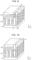
- FIG. 8 is a perspective view depicting a process of forming another stacked body on the stacked body
- FIG. 9 is a perspective view depicting a process of forming a second groove in the other stacked body
- FIG. 10 is a perspective view depicting a process of embedding an insulator in the second groove
- FIG. 11 is a perspective view depicting a process of forming holes in the two stacked bodies
- FIG. 12 is a schematic plan view of a semiconductor memory device according to a second embodiment
- FIG. 13 is a sectional view taken along the cutting-plane line C-C depicted in FIG. 12 ;
- FIG. 14 is a sectional view of principal portions of a semiconductor memory device according to some embodiments.
- Embodiments disclosed herein provide a semiconductor memory device that can improve product performance and reliability.
- a semiconductor memory device includes a substrate; a stacked body that is provided on the substrate and includes a first stacked body which is formed of a plurality of stacked first electrode layers and a second stacked body which is provided on the first stacked body and includes at least one second electrode layer; a hole that passes through the first stacked body and the second stacked body in a first direction perpendicular to the substrate and has a first insulator; and a channel film that is located between the first insulator and the first electrode layers and between the first insulator and the second electrode layer and has a first portion and a second portion which face each other with the first insulator placed therebetween.
- a first memory unit that is located between the first electrode layers and the first portion and a second memory unit that is located between the first electrode layers and the second portion are electrically insulated, and a third memory unit that is located between the second electrode layer and the first portion and a fourth memory unit that is located between the second electrode layer and the second portion are electrically connected.
- FIG. 1 is a schematic plan view of a semiconductor memory device according to a first embodiment.
- FIG. 2 is a sectional view taken along the cutting-plane line A-A depicted in FIG. 1 .
- FIG. 3 is a sectional view taken along the cutting-plane line B-B depicted in FIG. 1 .
- a semiconductor memory device 1 according to the present embodiment includes a semiconductor substrate 10 which is a silicon substrate, for example, a stacked body 20 , and memory cell films 30 .
- the stacked body 20 has a first region 21 provided on the semiconductor substrate 10 and a second region 22 provided on the first region 21 .
- electrode layers (word lines) 121 and insulating layers 122 which extend parallel to an X direction, are alternately stacked in a Z direction perpendicular to the X direction.
- the Z direction is a direction perpendicular to the substrate.
- selected gate electrode layers (selection gate electrode layers) (SGD) 221 and insulating layers 222 which are parallel to the X direction, are alternately stacked in the Z direction.
- the number of stacked electrode layers 121 and the number of stacked selected gate electrode layers 221 are not limited to particular numbers.
- FIG. 1 is a diagram showing the X-Y plane, which is viewed from above, of the selected gate electrode layer 221 depicted in FIGS. 2 and 3 , and the electrode layer 121 and a first groove 24 , which are located on the side closer to the substrate in the Z direction than the selected gate electrode layer 221 , are indicated by broken lines. Moreover, the insulating layer 222 is not depicted in the drawing.
- the electrode layers 121 and the selected gate electrode layers 221 are formed as conductive layers containing tungsten, for instance.
- the insulating layers 122 and the insulating layers 222 are formed as silicon oxide (SiO 2 ) layers, for instance.
- a dummy word line (not depicted in the drawing) which does not function as an electrode layer may be provided below the selected gate electrode layer 221 .
- the dummy word line is used to adjust a voltage between the electrode layers 121 and the selected gate electrode layers 221 , for example.
- the memory cell films 30 face each other with an insulator 40 (a first insulator) which is silicon oxide, for example, placed therebetween or surround the insulator 40 .
- the hole is surrounded by the second electrode, which is formed radially around the hole. That is, the second electrode is formed with an annular shape around the hole (i.e., a ring shape), so as to surround the hole in a radial direction.
- a plurality of holes 23 are arranged in a staggered manner in the X direction.
- An example of the structure of each memory cell film 30 will be briefly described with reference to FIG. 4 .
- FIG. 4 is a sectional view depicting an example of the structure of the memory cell film 30 .
- the memory cell film 30 has a memory film including a charge block film 31 , a charge storage film 32 , and a tunnel insulating film 33 and a channel film (a semiconductor layer) 34 .
- a memory cell transistor including the tunnel insulating film 33 , the charge storage film 32 , and the charge block film 31 is formed.
- the memory film and the channel film 34 are collectively depicted as the memory cell film 30 .
- the charge block film 31 and the tunnel insulating film 33 may be formed as silicon oxide films, for instance.
- the charge storage film 32 may be formed as a silicon nitride (SiN) film, for example.
- the channel film 34 may be formed as a polysilicon film, for instance. The channel film 34 is connected to a bit line 50 (see FIGS. 2 and 3 ) extending in a Y direction.
- the electrode layers 121 are divided by the first groove 24 extending in the X direction.
- an insulator 41 which is silicon oxide, for example, is embedded. That is, in the Y direction, an electrode 121 a and an electrode 121 b are formed via a first groove 24 a.
- the electrode 121 b and an electrode 121 c may be formed via a first groove 24 b provided parallel to the first groove 24 a in the X direction.
- each hole 23 has a memory cell transistor for each of the two electrodes which face each other.
- a memory cell transistor formation region is treated as a memory unit (a memory).
- the selected gate electrode layers 221 are not divided by the first grooves 24 a and 24 b, and the electrodes are continuous.
- the holes 23 are surrounded with the electrode layers 221 . That is, the outer periphery of the memory cell film 30 faces the electrode layers 221 .
- the selected gate electrode layers 221 have a second groove 25 that divides the selected gate electrode layers 221 by extending in the X direction.
- an insulator 42 which is silicon oxide, for example, is embedded.
- the selected gate electrode layers 221 include selected gate electrode layers 221 a and 221 b divided by the second groove 25 .
- the selected gate electrode layers 221 a and 221 b are electrically insulated from each other by the second groove 25 .
- a hole 23 H provided in a position in which the hole 23 H passes through the second groove 25 is not connected to the bit line 50 . That is, the hole 23 H formed in the second groove 25 is a dummy memory cell transistor.
- the structure depicted in FIGS. 1 to 3 has a stacked body 21 a including the electrode 121 a and formed of the layers stacked in the Z direction, a stacked body 21 b including the electrode 121 b and formed of the layers stacked in the Z direction, a stacked body 21 c including the electrode 121 c and formed of the layers stacked in the Z direction, and a stacked body 22 a provided over these stacked bodies 21 a, 21 b, and 21 c and having the same width as that of the stacked bodies 21 a, 21 b, and 21 c in the Y direction.
- a stacked body 210 is formed on the semiconductor substrate 10 .
- the stacked body 210 corresponds to the above-described first region 21 of the stacked body 20 .
- insulating layers 123 and the insulating layers 122 are alternately stacked.
- the insulating layers 123 are formed as silicon nitride layers, for example.
- An under layer may be provided between the semiconductor substrate 10 and the stacked body 210 .
- a cell source line or the like is possible.
- a plurality of first grooves 24 extending parallel to the X direction are formed.
- the stacked body 210 is divided.
- the insulator 41 is embedded in the first grooves 24 .
- a stacked body 220 is formed on the stacked body 210 .
- the stacked body 220 corresponds to the above-described second region 22 of the stacked body 20 .
- insulating layers 223 and the insulating layers 222 are alternately stacked.
- the insulating layers 223 are formed as silicon nitride layers, for example.
- the second groove 25 extending parallel to the X direction is formed. As a result, part of the stacked body 220 is divided.
- the second groove 25 is formed on the first groove 24 , for example.
- the insulator 42 is embedded in the second groove 25 .
- the holes 23 and 23 H are formed as depicted in FIG. 11 .
- the holes are formed so as to be aligned such that the holes pass through the insulator 41 embedded in the first grooves 24 of the stacked body 210 in the Z direction. That is, some holes 23 (the holes 23 H) are formed so as to pass through both the insulator 41 embedded in the first grooves 24 and the insulator 42 embedded in the second groove 25 .
- the memory cell films 30 are formed in the holes 23 and 23 H.
- an opening (not depicted in the drawing), which is different from the holes 23 , and passing through the stacked body 210 and the stacked body 220 , is formed.
- the insulating layers 123 are replaced with the electrode layers 121 and the insulating layers 223 are replaced with the selected gate electrode layers 221 .
- the semiconductor memory device 1 according to some embodiments is produced.
- the opening may have the shape of a hole or the shape of a slit that divides the stacked body.
- the selected gate electrode layers 221 are required to have high characteristics about on and off because the selected gate electrode layers 221 select the memory cell films 30 in operation units (i.e., the selection cells) at the time of writing and reading.
- operation units i.e., the selection cells
- a leakage current flowing through the division area may result in deterioration of the cutoff characteristics of a non-selected region.
- boost voltage of the non-selected region is reduced, leading to a reduction in product performance and a reduction in reliability such as the erasure of write data.
- the operation unit is, for example, a write unit (a page unit).
- each of the selected gate electrode layers 221 a and 221 b generated as a result of division by the second groove 25 is the operation unit.
- the number of electrode layers 121 configuring the operation unit, the number of first grooves 24 , and the number of bit lines 50 are not limited to any particular quantities.
- FIG. 12 is a schematic plan view of a semiconductor memory device according to a second embodiment.
- FIG. 13 is a sectional view taken along the cutting-plane line C-C depicted in FIG. 12 .
- FIGS. 12 and 13 component elements similar to those of the above-described first embodiment will be identified with the same reference signs and the detailed description thereof will be omitted.
- FIG. 12 is a diagram showing the X-Y plane, which is viewed from above, of the selected gate electrode layer 221 depicted in FIG. 13 , and the electrode layer 121 and the first grooves 24 , which are located on the side closer to the substrate in the Z direction than the selected gate electrode layer 221 , are indicated by broken lines.
- the insulating layer 222 is not depicted in the drawing.
- the second groove 25 that divides the selected gate electrode layers 221 is formed in the position in which the holes 23 H are formed in the second region 22 of the stacked body 20 .
- a slit 26 that divides the stacked body 20 is formed in a position which is different from the positions in which the holes 23 are formed.
- the slit 26 is provided in any position that divides the operation units, for example.
- the selected gate electrode layers 221 a and 221 b are formed via the slit 26 .
- the selected gate electrode layers 221 a and 221 b are electrically insulated from each other.
- an insulator 43 (a fourth insulator) which is silicon oxide, for instance, is embedded.
- This slit 26 is formed, in a position different from the positions in which the first grooves 24 are formed, as a through groove passing through the stacked bodies after the process (see FIG. 8 ) described in the first embodiment by which the stacked body 22 a is formed on the stacked body 21 a.
- the hole 23 H having a dummy memory cell transistor may be formed in the position in which the slit 26 is formed.
- the selected gate electrode layers 221 whose operation units are the same are continuous without being divided.
- product performance and reliability can be improved.
- the slit 26 is formed at the boundary of the operation units in one operation.
- FIG. 14 is a sectional view depicting the structure of principal portions of a semiconductor memory device according to some embodiments. Component elements similar to those of the above-described first embodiment will be identified with the same reference signs and the detailed description thereof will be omitted.
- a semiconductor memory device 3 according to this modification includes a lower layer stacked body and an upper layer stacked body which are divided parts of the first region 21 of the stacked body 20 .
- a stopper 60 is provided between the lower layer stacked body and the upper layer stacked body.
- the lower layer stacked body is located, in the Z direction, on the side where the substrate is located, and the upper layer stacked body is located on the lower layer stacked body.
- the lower layer stacked body and the upper layer stacked body have an equal number of stacked layers, for example, but the number of stacked layers is not limited to a particular number.
- a hole is first formed in the lower layer stacked body, the stopper 60 and the upper layer stacked body are then formed on the lower layer stacked body, and a hole is formed in the upper layer stacked body. In this way, the hole 23 is formed in stages. At this time, by placing the stopper 60 between the holes, the stopper 60 functions as an etching stopper film.
- the stopper 60 is formed as a polysilicon film, for example.
- the stopper 60 is formed of polysilicon, the channel film 34 of the lower layer stacked body and the channel film 34 of the upper layer stacked body are electrically connected to each other. Moreover, since the hole is formed in stages, there may be a slight difference between the hole position in the lower layer stacked body and the hole position in the upper layer stacked body. The number of stages for formation of the hole is not limited to two, and the hole may be formed in three or more stages.
- the first groove 24 in which the insulator is embedded and the hole 23 passing through the groove are formed in the lower layer stacked body, and the memory cell films 30 are formed in the hole 23 .
- the stopper 60 and the upper layer stacked body are formed on the lower layer stacked body, and the first groove 24 in which the insulator is embedded is formed so as to be located in almost the same position as the first groove 24 formed in the lower layer stacked body.
- the second region 22 of the stacked body is formed on the upper layer stacked body, and the following is the same as the method of the first embodiment depicted in FIG. 9 and the drawings that follow.
- the first groove 24 in which the insulator is embedded and the hole 23 passing through the groove are first formed in the lower layer stacked body, and the memory cell films 30 are formed in the hole 23 . Then, the stopper 60 and the upper layer stacked body are formed on the lower layer stacked body. Then, the first groove 24 in which the insulator is embedded is formed in a manner similar to the second embodiment, and the second region 22 of the stacked body is formed on the upper layer stacked body. A hole that passes through the upper layer stacked body and the second region 22 is formed, and the slit 26 that divides the lower layer, the upper layer, and the stacked body of the second region 22 is then formed.
- a sacrificial layer which is different from the material of the first groove 24 is embedded in the hole 23 .
- the sacrificial layer is a silicon nitride layer, for example.
- the upper layer stacked body is formed, and the first groove 24 is formed in the upper layer stacked body.
- the first groove 24 which is formed in the upper layer stacked body is aligned so as to be located in the same position, in the Z direction, as the first groove 24 formed in the lower layer stacked body. Then, by the method depicted in FIG.
- the second groove 25 and the hole 23 are formed.
- the lower end of the hole 23 formed in the upper layer stacked body reaches the sacrificial layer embedded in the hole 23 of the lower layer stacked body.
- An opening which is different from the hole 23 is formed, and the silicon nitride layers forming the stacked body and the sacrificial layer embedded in the hole 23 of the lower layer stacked body are removed.
- the memory cell films are formed, in one operation, in the hole 23 passing through the lower layer stacked body, the upper layer stacked body, and the second region 22 .
- a sacrificial layer is embedded in the hole 23 passing through the lower layer stacked body, the upper layer stacked body and the second region 22 are formed, and the hole 23 is formed therein so as to reach the sacrificial layer.
- the sacrificial layer is removed from the slit 26 , and the memory cell films are formed, in one operation, in the hole 23 passing through the lower layer stacked body, the upper layer stacked body, and the second region 22 .
- the selected gate electrode layers 221 whose operation units are the same are continuous without being divided by the first groove 24 .
- product performance and reliability can be improved.
Landscapes
- Semiconductor Memories (AREA)
- Non-Volatile Memory (AREA)
- Read Only Memory (AREA)
Abstract
Description
Claims (16)
Applications Claiming Priority (2)
| Application Number | Priority Date | Filing Date | Title |
|---|---|---|---|
| JP2018052841A JP2019165150A (en) | 2018-03-20 | 2018-03-20 | Semiconductor storage device |
| JP2018-052841 | 2018-03-20 |
Publications (2)
| Publication Number | Publication Date |
|---|---|
| US20190296037A1 US20190296037A1 (en) | 2019-09-26 |
| US10692883B2 true US10692883B2 (en) | 2020-06-23 |
Family
ID=67984515
Family Applications (1)
| Application Number | Title | Priority Date | Filing Date |
|---|---|---|---|
| US16/114,045 Expired - Fee Related US10692883B2 (en) | 2018-03-20 | 2018-08-27 | Semiconductor memory device |
Country Status (2)
| Country | Link |
|---|---|
| US (1) | US10692883B2 (en) |
| JP (1) | JP2019165150A (en) |
Cited By (1)
| Publication number | Priority date | Publication date | Assignee | Title |
|---|---|---|---|---|
| US12160991B2 (en) | 2020-12-24 | 2024-12-03 | Samsung Electronics Co., Ltd. | Semiconductor device and data storage system including the same |
Citations (6)
| Publication number | Priority date | Publication date | Assignee | Title |
|---|---|---|---|---|
| US20050196922A1 (en) * | 2004-03-08 | 2005-09-08 | Josef Willer | Method for producing semiconductor memory devices and integrated memory device |
| JP2013093577A (en) | 2011-10-26 | 2013-05-16 | Sk Hynix Inc | Three-dimensional nonvolatile memory element and method of manufacturing the same |
| US20140043916A1 (en) * | 2012-08-13 | 2014-02-13 | Sandisk Technologies Inc. | Erase For 3D Non-Volatile Memory With Sequential Selection Of Word Lines |
| US20150255486A1 (en) | 2014-03-05 | 2015-09-10 | Kabushiki Kaisha Toshiba | Nonvolatile semiconductor storage device |
| US20160268279A1 (en) * | 2015-03-12 | 2016-09-15 | Kabushiki Kaisha Toshiba | Semiconductor memory device |
| JP2016171280A (en) | 2015-03-16 | 2016-09-23 | 株式会社東芝 | Manufacturing method of semiconductor memory device |
-
2018
- 2018-03-20 JP JP2018052841A patent/JP2019165150A/en active Pending
- 2018-08-27 US US16/114,045 patent/US10692883B2/en not_active Expired - Fee Related
Patent Citations (9)
| Publication number | Priority date | Publication date | Assignee | Title |
|---|---|---|---|---|
| US20050196922A1 (en) * | 2004-03-08 | 2005-09-08 | Josef Willer | Method for producing semiconductor memory devices and integrated memory device |
| JP2013093577A (en) | 2011-10-26 | 2013-05-16 | Sk Hynix Inc | Three-dimensional nonvolatile memory element and method of manufacturing the same |
| US9117700B2 (en) | 2011-10-26 | 2015-08-25 | SK Hynix Inc. | 3-D nonvolatile memory devices and methods of manufacturing the same |
| US20140043916A1 (en) * | 2012-08-13 | 2014-02-13 | Sandisk Technologies Inc. | Erase For 3D Non-Volatile Memory With Sequential Selection Of Word Lines |
| US20150255486A1 (en) | 2014-03-05 | 2015-09-10 | Kabushiki Kaisha Toshiba | Nonvolatile semiconductor storage device |
| JP2015170643A (en) | 2014-03-05 | 2015-09-28 | 株式会社東芝 | Nonvolatile semiconductor memory device |
| US20160268279A1 (en) * | 2015-03-12 | 2016-09-15 | Kabushiki Kaisha Toshiba | Semiconductor memory device |
| JP2016171280A (en) | 2015-03-16 | 2016-09-23 | 株式会社東芝 | Manufacturing method of semiconductor memory device |
| US9786679B2 (en) | 2015-03-16 | 2017-10-10 | Toshiba Memory Corporation | Method for manufacturing semiconductor memory device |
Cited By (1)
| Publication number | Priority date | Publication date | Assignee | Title |
|---|---|---|---|---|
| US12160991B2 (en) | 2020-12-24 | 2024-12-03 | Samsung Electronics Co., Ltd. | Semiconductor device and data storage system including the same |
Also Published As
| Publication number | Publication date |
|---|---|
| JP2019165150A (en) | 2019-09-26 |
| US20190296037A1 (en) | 2019-09-26 |
Similar Documents
| Publication | Publication Date | Title |
|---|---|---|
| US20220173032A1 (en) | Semiconductor memory device | |
| US10971515B2 (en) | Semiconductor memory device | |
| US10832776B2 (en) | Semiconductor device and semiconductor memory device | |
| US10553603B2 (en) | Semiconductor device and method for manufacturing semiconductor device | |
| US10056150B2 (en) | Non-volatile semiconductor memory device | |
| US20210384215A1 (en) | Semiconductor storage device | |
| US11289505B2 (en) | Semiconductor memory device | |
| JP2008186868A (en) | Nonvolatile semiconductor memory device | |
| TWI714211B (en) | Semiconductor memory device | |
| CN114203712A (en) | Semiconductor memory device with a plurality of memory cells | |
| TWI793430B (en) | semiconductor memory device | |
| TW202111932A (en) | Semiconductor memory device and method of manufacturing the same | |
| US20220415416A1 (en) | Systems and methods for compensating for erase speed variations due to semi-circle sgd | |
| US10396091B2 (en) | Semiconductor memory device | |
| US12543309B2 (en) | Semiconductor storage device and method of manufacturing semiconductor storage device | |
| US10692883B2 (en) | Semiconductor memory device | |
| US10797069B2 (en) | Semiconductor memory device | |
| US11600629B2 (en) | Semiconductor memory device and method of manufacturing semiconductor memory device | |
| US20220302023A1 (en) | Semiconductor device and manufacturing method thereof | |
| US20230072833A1 (en) | Semiconductor memory device | |
| US12507415B2 (en) | Semiconductor memory device | |
| US11462562B2 (en) | Semiconductor device | |
| US20250107085A1 (en) | Semiconductor memory device and method of manufacturing the same | |
| US20240244852A1 (en) | Memory device | |
| US20220285440A1 (en) | Semiconductor storage device |
Legal Events
| Date | Code | Title | Description |
|---|---|---|---|
| FEPP | Fee payment procedure |
Free format text: ENTITY STATUS SET TO UNDISCOUNTED (ORIGINAL EVENT CODE: BIG.); ENTITY STATUS OF PATENT OWNER: LARGE ENTITY |
|
| STPP | Information on status: patent application and granting procedure in general |
Free format text: NON FINAL ACTION MAILED |
|
| STPP | Information on status: patent application and granting procedure in general |
Free format text: RESPONSE TO NON-FINAL OFFICE ACTION ENTERED AND FORWARDED TO EXAMINER |
|
| STPP | Information on status: patent application and granting procedure in general |
Free format text: NOTICE OF ALLOWANCE MAILED -- APPLICATION RECEIVED IN OFFICE OF PUBLICATIONS |
|
| AS | Assignment |
Owner name: TOSHIBA MEMORY CORPORATION, JAPAN Free format text: ASSIGNMENT OF ASSIGNORS INTEREST;ASSIGNOR:UCHIYAMA, YASUHIRO;REEL/FRAME:052182/0291 Effective date: 20180820 |
|
| STPP | Information on status: patent application and granting procedure in general |
Free format text: PUBLICATIONS -- ISSUE FEE PAYMENT RECEIVED |
|
| STCF | Information on status: patent grant |
Free format text: PATENTED CASE |
|
| AS | Assignment |
Owner name: K.K. PANGEA, JAPAN Free format text: MERGER;ASSIGNOR:TOSHIBA MEMORY CORPORATION;REEL/FRAME:055659/0471 Effective date: 20180801 Owner name: KIOXIA CORPORATION, JAPAN Free format text: CHANGE OF NAME AND ADDRESS;ASSIGNOR:TOSHIBA MEMORY CORPORATION;REEL/FRAME:055669/0001 Effective date: 20191001 Owner name: TOSHIBA MEMORY CORPORATION, JAPAN Free format text: CHANGE OF NAME AND ADDRESS;ASSIGNOR:K.K. PANGEA;REEL/FRAME:055669/0401 Effective date: 20180801 |
|
| FEPP | Fee payment procedure |
Free format text: MAINTENANCE FEE REMINDER MAILED (ORIGINAL EVENT CODE: REM.); ENTITY STATUS OF PATENT OWNER: LARGE ENTITY |
|
| LAPS | Lapse for failure to pay maintenance fees |
Free format text: PATENT EXPIRED FOR FAILURE TO PAY MAINTENANCE FEES (ORIGINAL EVENT CODE: EXP.); ENTITY STATUS OF PATENT OWNER: LARGE ENTITY |
|
| STCH | Information on status: patent discontinuation |
Free format text: PATENT EXPIRED DUE TO NONPAYMENT OF MAINTENANCE FEES UNDER 37 CFR 1.362 |
|
| FP | Lapsed due to failure to pay maintenance fee |
Effective date: 20240623 |