US10692707B2 - RF substrate bias with high power impulse magnetron sputtering (HIPIMS) - Google Patents
RF substrate bias with high power impulse magnetron sputtering (HIPIMS) Download PDFInfo
- Publication number
- US10692707B2 US10692707B2 US13/859,854 US201313859854A US10692707B2 US 10692707 B2 US10692707 B2 US 10692707B2 US 201313859854 A US201313859854 A US 201313859854A US 10692707 B2 US10692707 B2 US 10692707B2
- Authority
- US
- United States
- Prior art keywords
- magnetron
- pulse
- switch
- hipims
- substrate
- Prior art date
- Legal status (The legal status is an assumption and is not a legal conclusion. Google has not performed a legal analysis and makes no representation as to the accuracy of the status listed.)
- Active, expires
Links
Images


Classifications
-
- H—ELECTRICITY
- H01—ELECTRIC ELEMENTS
- H01J—ELECTRIC DISCHARGE TUBES OR DISCHARGE LAMPS
- H01J37/00—Discharge tubes with provision for introducing objects or material to be exposed to the discharge, e.g. for the purpose of examination or processing thereof
- H01J37/32—Gas-filled discharge tubes
- H01J37/34—Gas-filled discharge tubes operating with cathodic sputtering
- H01J37/3411—Constructional aspects of the reactor
- H01J37/3444—Associated circuits
-
- H—ELECTRICITY
- H01—ELECTRIC ELEMENTS
- H01J—ELECTRIC DISCHARGE TUBES OR DISCHARGE LAMPS
- H01J37/00—Discharge tubes with provision for introducing objects or material to be exposed to the discharge, e.g. for the purpose of examination or processing thereof
- H01J37/32—Gas-filled discharge tubes
- H01J37/32917—Plasma diagnostics
- H01J37/32935—Monitoring and controlling tubes by information coming from the object and/or discharge
- H01J37/32944—Arc detection
-
- C—CHEMISTRY; METALLURGY
- C23—COATING METALLIC MATERIAL; COATING MATERIAL WITH METALLIC MATERIAL; CHEMICAL SURFACE TREATMENT; DIFFUSION TREATMENT OF METALLIC MATERIAL; COATING BY VACUUM EVAPORATION, BY SPUTTERING, BY ION IMPLANTATION OR BY CHEMICAL VAPOUR DEPOSITION, IN GENERAL; INHIBITING CORROSION OF METALLIC MATERIAL OR INCRUSTATION IN GENERAL
- C23C—COATING METALLIC MATERIAL; COATING MATERIAL WITH METALLIC MATERIAL; SURFACE TREATMENT OF METALLIC MATERIAL BY DIFFUSION INTO THE SURFACE, BY CHEMICAL CONVERSION OR SUBSTITUTION; COATING BY VACUUM EVAPORATION, BY SPUTTERING, BY ION IMPLANTATION OR BY CHEMICAL VAPOUR DEPOSITION, IN GENERAL
- C23C14/00—Coating by vacuum evaporation, by sputtering or by ion implantation of the coating forming material
- C23C14/22—Coating by vacuum evaporation, by sputtering or by ion implantation of the coating forming material characterised by the process of coating
- C23C14/34—Sputtering
- C23C14/3435—Applying energy to the substrate during sputtering
- C23C14/345—Applying energy to the substrate during sputtering using substrate bias
-
- C—CHEMISTRY; METALLURGY
- C23—COATING METALLIC MATERIAL; COATING MATERIAL WITH METALLIC MATERIAL; CHEMICAL SURFACE TREATMENT; DIFFUSION TREATMENT OF METALLIC MATERIAL; COATING BY VACUUM EVAPORATION, BY SPUTTERING, BY ION IMPLANTATION OR BY CHEMICAL VAPOUR DEPOSITION, IN GENERAL; INHIBITING CORROSION OF METALLIC MATERIAL OR INCRUSTATION IN GENERAL
- C23C—COATING METALLIC MATERIAL; COATING MATERIAL WITH METALLIC MATERIAL; SURFACE TREATMENT OF METALLIC MATERIAL BY DIFFUSION INTO THE SURFACE, BY CHEMICAL CONVERSION OR SUBSTITUTION; COATING BY VACUUM EVAPORATION, BY SPUTTERING, BY ION IMPLANTATION OR BY CHEMICAL VAPOUR DEPOSITION, IN GENERAL
- C23C14/00—Coating by vacuum evaporation, by sputtering or by ion implantation of the coating forming material
- C23C14/22—Coating by vacuum evaporation, by sputtering or by ion implantation of the coating forming material characterised by the process of coating
- C23C14/34—Sputtering
- C23C14/3485—Sputtering using pulsed power to the target
-
- H—ELECTRICITY
- H01—ELECTRIC ELEMENTS
- H01J—ELECTRIC DISCHARGE TUBES OR DISCHARGE LAMPS
- H01J37/00—Discharge tubes with provision for introducing objects or material to be exposed to the discharge, e.g. for the purpose of examination or processing thereof
- H01J37/32—Gas-filled discharge tubes
- H01J37/32009—Arrangements for generation of plasma specially adapted for examination or treatment of objects, e.g. plasma sources
- H01J37/32018—Glow discharge
- H01J37/32045—Circuits specially adapted for controlling the glow discharge
-
- H—ELECTRICITY
- H01—ELECTRIC ELEMENTS
- H01J—ELECTRIC DISCHARGE TUBES OR DISCHARGE LAMPS
- H01J37/00—Discharge tubes with provision for introducing objects or material to be exposed to the discharge, e.g. for the purpose of examination or processing thereof
- H01J37/32—Gas-filled discharge tubes
- H01J37/34—Gas-filled discharge tubes operating with cathodic sputtering
- H01J37/3402—Gas-filled discharge tubes operating with cathodic sputtering using supplementary magnetic fields
- H01J37/3405—Magnetron sputtering
- H01J37/3408—Planar magnetron sputtering
-
- H—ELECTRICITY
- H01—ELECTRIC ELEMENTS
- H01J—ELECTRIC DISCHARGE TUBES OR DISCHARGE LAMPS
- H01J37/00—Discharge tubes with provision for introducing objects or material to be exposed to the discharge, e.g. for the purpose of examination or processing thereof
- H01J37/32—Gas-filled discharge tubes
- H01J37/34—Gas-filled discharge tubes operating with cathodic sputtering
- H01J37/3464—Operating strategies
- H01J37/3467—Pulsed operation, e.g. HIPIMS
-
- C—CHEMISTRY; METALLURGY
- C23—COATING METALLIC MATERIAL; COATING MATERIAL WITH METALLIC MATERIAL; CHEMICAL SURFACE TREATMENT; DIFFUSION TREATMENT OF METALLIC MATERIAL; COATING BY VACUUM EVAPORATION, BY SPUTTERING, BY ION IMPLANTATION OR BY CHEMICAL VAPOUR DEPOSITION, IN GENERAL; INHIBITING CORROSION OF METALLIC MATERIAL OR INCRUSTATION IN GENERAL
- C23C—COATING METALLIC MATERIAL; COATING MATERIAL WITH METALLIC MATERIAL; SURFACE TREATMENT OF METALLIC MATERIAL BY DIFFUSION INTO THE SURFACE, BY CHEMICAL CONVERSION OR SUBSTITUTION; COATING BY VACUUM EVAPORATION, BY SPUTTERING, BY ION IMPLANTATION OR BY CHEMICAL VAPOUR DEPOSITION, IN GENERAL
- C23C14/00—Coating by vacuum evaporation, by sputtering or by ion implantation of the coating forming material
- C23C14/22—Coating by vacuum evaporation, by sputtering or by ion implantation of the coating forming material characterised by the process of coating
- C23C14/34—Sputtering
- C23C14/35—Sputtering by application of a magnetic field, e.g. magnetron sputtering
-
- H—ELECTRICITY
- H01—ELECTRIC ELEMENTS
- H01J—ELECTRIC DISCHARGE TUBES OR DISCHARGE LAMPS
- H01J37/00—Discharge tubes with provision for introducing objects or material to be exposed to the discharge, e.g. for the purpose of examination or processing thereof
- H01J37/32—Gas-filled discharge tubes
- H01J37/32009—Arrangements for generation of plasma specially adapted for examination or treatment of objects, e.g. plasma sources
- H01J37/32055—Arc discharge
- H01J37/32064—Circuits specially adapted for controlling the arc discharge
Definitions
- the present invention relates generally to sputtering, and more particularly, to high power impulse magnetron sputtering (HIPIMS).
- HIPIMS high power impulse magnetron sputtering
- Sputtering is a physical process whereby atoms in a solid target material are ejected into the gas phase due to bombardment of the material by energetic ions.
- the process of sputtering is commonly used for thin-film deposition.
- the energetic ions for the sputtering process are supplied by a plasma that is induced in the sputtering equipment.
- a variety of techniques are used to modify the plasma properties, especially ion density, to achieve the optimum sputtering conditions.
- Some of the techniques that are used to modify the plasma properties include the usage of RF (radio frequency) alternating current, an AC power source, a DC power source, a superposition of DC and AC power sources, a pulsed DC power source such as a bipolar or unipolar power source, the utilization of magnetic fields, and the application of a bias voltage to the target.
- RF radio frequency
- Sputtering sources are usually magnetrons that utilize magnetic fields to trap electrons in a closed plasma loop close to the surface of a target.
- the electrons follow helical paths in a loop around the magnetic field lines.
- the electrons undergo more ionizing collisions with gaseous neutrals near the target surface than would otherwise occur.
- the sputter gas is inert, typically argon, though other gases can be used.
- the extra argon ions created as a result of these collisions leads to a relatively higher deposition rate.
- a racetrack can be formed, which is the area of preferred erosion of material.
- movable magnetic arrangements are being used, that allow for sweeping the plasma loop over relatively larger areas of the target.
- Direct current (DC) magnetron sputtering is a well-known technique using crossed electric and magnetic fields.
- An enhancement of DC magnetron sputtering is pulsed DC.
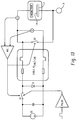
- the technique uses a so-called “chopper,” where an inductor coil L and a switch are used to modify a DC power supply into a supply of unipolar or bipolar pulses, see FIG. 1 .
- the inductor coil L is the chopper and can preferably include a tap located between the DC power supply and the magnetron cathode.
- the electronic switch S is periodically open and closed to create the pulses.
- an effective shortcut between the tap of the coil L and the magnetron anode switches the negative cathode voltage off, preferably overshooting to positive voltages by the auto transforming effect of coil L.
- the current from the DC power supply continues to flow into the coil L and storing energy in its magnetic field.
- a short negative high voltage peak is formed at the magnetron cathode. This helps for relatively fast reigniting of the magnetron plasma and restoring the original discharge current.
- the High Power Impulse Magnetron Sputtering (HIPIMS) technology as described in the prior art uses relatively lower repetition frequency of pulses typically 5 Hz to 200 Hz, and pulse times 20 to 500 ⁇ s.
- the discharge peak currents range from 100 A for relatively small cathodes up to 4 kA for relatively large cathodes, which corresponds to current density at cathode in the order of magnitude of 0.1 to 10 A/cm2.
- a common technique uses wiring as in FIG. 1 .
- the work piece holder is either on an external potential, such as a DC potential, or the work piece holder is left on a floating potential in the plasma.
- the prior art design of FIG. 1 involves applying a DC bias to the workpiece holder.
- FIG. 2 shows the result of an experiment.
- the data shows the measured rise time of the current as a function of frequency in a state of the art HIPIMS discharge.
- the target in this example was made of Tantalum (Ta), with the target having a diameter of 300 mm, and the experiment was using a rotating magnet array.
- Ta Tantalum
- an apparatus for generating sputtering of a target to produce a coating on a substrate comprises a magnetron including a cathode and an anode.
- a power supply is operably connected to the magnetron and at least one capacitor is operably connected to the power supply.
- a first switch is also provided. The first switch operably connects the power supply to the magnetron to charge the magnetron and the first switch is configured to charge the magnetron according to a first pulse.
- An electrical bias device is operably connected to the substrate and configured to apply a substrate bias.
- a chuck is operably connected to the electrical bias device where the substrate is located on the chuck.
- a coil is operably connected to the at least one capacitor.
- a second switch is operably connected to discharge the magnetron and connected at a point along the coil.
- the second switch is configured to discharge the magnetron according to a second pulse.
- At least one detector is operably connected to the magnetron where the at least one detector is configured for detecting an arc that is forming.
- the first switch and the second switch are controlled in response to a detection of the arc by the at least one detector to inhibit a formation of the arc.
- a method of applying a substrate bias in an apparatus for generating sputtering to produce a coating on a substrate includes the step of applying a first pulse to a first switch to charge a magnetron from a power supply. The method further includes the step of applying the substrate bias from an electrical bias device operably connected to the substrate.
- FIG. 1 is a prior art schematic of a HIPIMS application
- FIG. 2 is a plot illustrating the voltage and amps of an HIPIMS application in the prior art during a typical pulse
- FIG. 3 is a first example schematic of the subject invention with an RF generator
- FIG. 4 is a plot illustrating the voltage and amps of an HIPIMS application in the prior art during a typical pulse when an RF is off;
- FIG. 5 is a plot illustrating the voltage and amps of an HIPIMS application during a typical pulse when a low power RF is used on the chuck of FIG. 3 ;
- FIG. 6 is a plot illustrating the voltage and amps of an HIPIMS application during a typical pulse when a relatively higher power RF is used on the chuck of FIG. 3 ;
- FIG. 7 is a schematic of an HIPIMS application showing the bottom thickness of the substrate when no RF bias is used
- FIG. 8 is a schematic of an HIPIMS application showing the bottom thickness of the substrate when RF bias is used
- FIG. 9 is a second example schematic of the subject invention using RF bias in combination with two switches for applying different modes
- FIG. 10 is an example schematic of a high frequency mode for use with FIG. 9 ;
- FIG. 11 is an example schematic of a multiple sub-pulse mode within a main pulse that is used with FIG. 9 ;
- FIG. 12 is an example schematic of a pulsed pre-ionization mode for use with FIG. 9 ;
- FIG. 13 is a third example schematic of the subject invention using RF bias in combination with two switches and an arc detection design.
- FIG. 14 is a fourth example schematic of the subject invention using RF bias in combination with two switches for applying different modes and an arc detection design.
- FIG. 3 shows a first example schematic of the subject invention.
- the invention can use standard HIPIMS wiring, such as the wiring in FIG. 1 , but in addition, an electrical bias device 10 , such as an RF generator, is connected to a substrate 14 .
- the electrical bias device can be connected to a chuck 12 that holds the substrate 14 .
- This first example can include a magnetron including a cathode and an anode, a target located near the magnetron where the target is used for sputtering atoms to produce the coating on the substrate, a power supply operably connected to the magnetron, at least one capacitor C operably connected to the power supply, and a first switch S 1 operably connected to charge the magnetron and configured for administering a first pulse to the magnetron.
- an electrical bias device 10 such as an RF generator
- the chuck 12 can be a wafer pedestal which holds a substrate 14 .
- the substrate 14 in this example is a wafer, but the substrate can also be other materials for other applications as well.
- the distance between the magnetron and the chuck 12 is relatively small and is generally between 20 mm to 100 mm. A test experiment was performed at 50 mm. Some magnetic field lines of the magnetron, preferably in the form of an unbalanced magnetron field, reach the chuck 12 with a magnetic field intensity of at least 10 Gauss. This way, magnetic confinement improves the stability of the RF discharge when the magnetron plasma is off. At the same time, the remaining RF discharge between pulses serves as a pre-ionization for the HIPIMS discharge, in one example method.
- the HIPIMS pulse can be provided in the example of FIG. 3 through the first switch S 1 that is operably connected to charge a magnetron and is configured to charge the magnetron according to the first pulse.
- Combining an electrical bias device 10 , such as an RF generator, connected to a chuck 12 can usually result in a relatively faster, more reliable ignition of an HIPIMS pulse.
- the time delay between the pulses is shorter, the energy delivered for charging the capacitors between the pulses is relatively smaller and the capacitors can have a lower capacity, which results in relatively smaller dimensions and lower cost. Shorter pulses with relatively higher frequencies can be provided with use of the method of the subject invention.
- a RF bias such as a capacitive RF bias
- the RF bias usually reduces or even eliminates arcing and substrate or wafer damage.
- the RF bias works on insulating surfaces, such as in trenches and vias that use oxide materials.
- An additional advantage of using an RF bias over an ICP coil is that a shorter target-substrate distance can be used due to not requiring an ICP coil between the magnetron and the substrate.
- a relatively higher deposition rate occurs due to the fact that fewer parts are in the reactor and as a result of a shorter target-substrate distance.
- FIGS. 4-6 illustrate the benefit of providing an electrical bias device, such as a RF generator, connected to a chuck.
- FIGS. 4-6 were obtained by using an Oerlikon ClusterLine CL200 with a Cathode type ARQ151.
- the target for these example plots was made of Tantalum (Ta), with the target having a diameter of 300 mm.
- the gas flow rate is the amount of gas transferred into a chamber housing the target and the substrate.
- the pulse in the example plots has a frequency of 500 Hz, an on-time of 15 ⁇ s, and a voltage of approximately 1400V. Thus, this frequency can be applied through the first pulse.
- FIG. 4 shows a plot illustrating the voltage and amps of an HIPIMS application in the prior art during a typical pulse without the use of an electrical bias device, such as a RF generator.
- FIG. 4 thus is an example of the prior art and shows a typical delay of about 10 ⁇ s for the current to rise during a HIPIMS pulse. Only in the last 5 ⁇ s of the on-time does the current rise to a peak value of approximately 980 A.
- FIG. 5 shows a plot illustrating the voltage and amps of an HIPIMS application during a typical pulse when an RF generator is used to apply a relatively lower power RF load of 17 W with a self-bias of 10V is used on the chuck of FIG. 3 .
- Both the RF power load and self-bias voltage mentioned here are time-averaged values determined over several pulse periods.
- the delay between the start of a pulse, such as during the first pulse, and the beginning of the current rising is much shorter, as it is approximately 1.8 ⁇ s.
- the current in this example rises to a much higher peak current value of approximately 1580 A, in comparison to the peak value of 980 A when an RF is not used.
- FIG. 6 shows a plot illustrating the voltage and amps of an HIPIMS application during a typical pulse when a relatively higher power RF of 132 W with a self-bias of 103V is used on the chuck of FIG. 3 , again measured as time-average.
- the delay for the current beginning to rise between the start of a pulse, such as during the first pulse, and the beginning of the current rising is even shorter than in the lower power RF application of FIG. 5 , as the delay is approximately 0.8 ⁇ s.
- the current rises even relatively faster and the higher RF power usually results in a relatively higher self-bias potential of approximately 103V.
- the peak value of the current is approximately 1500 A in this example.
- Providing RF power also enables the HIPIMS impulse, applied by the first switch S 1 , to start at a relatively lower pressure range.
- the gas pressure corresponding to this flow rate was about 3 ⁇ 10 ⁇ 3 mbar.
- a HIPIMS impulse can occur with an RF power of greater than 50 W under the same argon gas flow conditions. With an RF power of greater than 50 W, the HIPIMS impulse starts repeatedly.
- Other low pressure operations are also possible and the argon gas flow of 15 sccm is just one example of an application of the subject invention.
- FIG. 7 and FIG. 8 illustrate the improved bottom coverage of the target.
- a Tantalum (Ta) target was used for deposition of a trench of approximately 180 ⁇ m deep and 50 ⁇ m wide.
- FIG. 7 shows the results of coverage on the substrate without the use of RF bias.
- FIG. 7 shows that a bottom thickness of approximately 251 nm was measured.
- the top thickness was measured at only 1.7 ⁇ m, resulting in only approximately 15% bottom coverage.
- FIG. 8 the results of using RF bias is shown.
- An example method of the subject invention involves applying a substrate bias in an apparatus for generating sputtering where pulses are applied to produce a coating on a substrate.
- One step in this method is to apply a first pulse to a first switch to charge a magnetron from a power supply.
- Another step in this example method is to apply a substrate bias from an electrical bias device that is operably connected to the substrate.
- the example method can also include the step of using an RF discharge of the RF generator during the first pulse, or rather, between pulses occurring with the first pulse pattern. Using the RF discharge during the first pulse, such as the HIPIMS pulse, will achieve a pre-ionization for the discharge of the magnetron.
- the RF power can be utilized to etch and pre-clean the substrate prior to deposition.
- Etching of a substrate such as selective sputtering or sputter-cleaning of topmost layers such as surface oxides, can be done under a closed shutter to avoid contamination of the target. Deposition of the substrate can then start after the shutter is opened.
- the method can further include the step of adjusting a voltage of the substrate bias to regulate the energy of ions bombarding the substrate to provide a desired coating for the substrate.
- the RF power can be applied in a pulsed mode of operation.
- the apparatus can be synchronized with the HIPIMS pulsing.
- the RF pulse can be started first, and then the HIPIMS magnetron pulse can be applied through the use of the first switch S 1 .
- the RF pulse can be switched off before the HIPIMS voltage pulse switches off.
- the RF pulse can be switched off after the HIPIMS voltage pulse switches off.
- the method and the device of the subject invention of providing an electrical bias device 10 can be combined with two switches for applying varying modes, including HIPIMS and a high frequency HIPIMS mode, as seen in FIG. 9 .
- the electrical bias device 10 such as an RF generator, is operably connected to the substrate 14 , such as to a chuck 12 which holds the substrate 14 .
- the example of the subject invention of FIG. 9 includes a first switch S 1 and a second switch S 2 in this design.
- the first switch S 1 is operably connected to charge the magnetron and is configured to administer a first voltage and can charge the magnetron according to a first pulse.
- the second switch S 2 is operably connected to discharge the magnetron and can be configured to discharge the magnetron according to a second pulse.
- the coil L in FIG. 9 can be provided that is operably connected to the at least one capacitor C.
- the coil L limits the slope of the magnetron discharge current rise.
- the coil L also limits the peak current when an arc occurs.
- pulse form for the first switch S 1 the first pulse
- has a high frequency
- Example pulse shapes for the first pulse of the first switch S 1 and the second pulse of the second switch S 2 are shown in the schematic of FIG. 10 for this high frequency mode.
- the high frequency mode of FIG. 10 can be operated at different levels, including a high frequency pulsed operation of 500 Hz-100 kHz, with preferable examples occurring between 1 kHz to 20 kHz.
- a relatively low effective duty cycle (0.1% to 10%) with lower power losses can also be achieved in this mode.
- An on-time (time period of t 1 ⁇ t 0 ) of 0.2 ⁇ s to 100 ⁇ s can be used in this example, with preferable examples occurring from 2 ⁇ s to 20 ⁇ s.
- the high frequency mode can start with connecting the charged capacitor C to the coil L at time t 0 .
- the charged capacitor can be at least one capacitor and the drawings can refer to a plurality of capacitors.
- Activating the switch S 2 to be opened at time t 2 ignites the plasma, after a delay of time (t 2 ⁇ t 0 ).
- the energy stored in the coil L can result in a voltage overshoot that occurs almost immediately on the magnetron cathode and in a relatively faster rise time of the magnetron current, as shown in the example of FIG. 10 .
- the magnetron discharge current decays between time t 1 (S 1 is off) and t 3 (S 2 is on).
- the time t 3 can be chosen between short times after t 1 to relatively long times, including the rest of the period.
- Each first pulse in the example mode of FIG. 10 starts with the voltage overshoot and the relatively fast rise of current during the same initial time period of (t 2 ⁇ t 0 ).
- the energy effectiveness is reached by a relatively long off-time for the first switch S 1 that is used for charging the capacitor C. This time period is shown by the period before t 0 occurs.
- the initial time period (t 2 ⁇ t 0 ) is relatively short and is used to store energy in the coil L.
- the relatively short time elapses when the first switch S 1 is activated to store energy in the coil L before the second pulse activates the second switch S 2 .
- the activation of the second switch S 2 causes a discharging of the magnetron. From a time t 0 ⁇ t 1 the charge of the capacitor C loads the coil L and discharging of the current of the magnetron takes place. Specifically, the magnetron discharge takes place from a time t 2 ⁇ t 3 . From a time t 1 ⁇ t 3 the rest energy from the coil L is discharged into the magnetron.
- FIG. 11 A second mode of operation for the example of FIG. 9 is shown in FIG. 11 .
- the second pulse exerts multiple sub-pulses that are formed within one main HIPIMS pulse of the first pulse.
- the first pulse can be a single, relatively long pulse to administer a voltage to the magnetron, and the first pulse is formed by using the first switch S 1 , during the time period t 1 ⁇ t 0 .
- the second pulse can be a multiple of sub-pulses, or a series of shorter sub-pulses, that are then formed at switch S 2 , as shown in the example of the mode in FIG. 11 .
- the first pulse has a duty cycle (0.1% to 10%) can be used in this mode.
- an on-time time period of t 1 ⁇ t 0
- the second pulse on-time time period of t 3 ⁇ t 2 , which is equal to ⁇ t on
- the second pulse off-time (time period of ⁇ t off ) can be 0.2 ⁇ s to 100 ⁇ s, with preferable examples of 2 ⁇ s to 20 ⁇ s.
- the second pulse duty cycle can have a wide range of values.
- the second pulse duty cycle ( ⁇ t on )/( ⁇ t on + ⁇ t off ) can range from 30% to 99%. It is thus appreciated that many different types of pulse configurations can be devised involving different types of constant and varied time periods for the second pulses. For example, even the ⁇ t on can have different amounts of time during each second pulse within a single main HIPIMS pulse of S 1 .
- the time period t 1 ⁇ t 0 is used to charge the capacitor C, load the coil L, and discharge the current of the magnetron.
- the second pulse, or rather the first sub-pulse can start with a proper delay when the switch S 2 opens.
- the charge of the capacitor C loads the coil L only.
- the energy stored in the coil L can result in a voltage overshoot on the magnetron cathode and in a relatively faster rise time of the magnetron current.
- the second pulse then can exert a sequence of shorter pulses by switching S 2 open and closed. Each of the pulses within the second pulse can start with a voltage overshoot and a relatively fast rise of current.
- the magnetron discharge takes place from a time t 2 ⁇ t 3 , each time S 2 is turned on. During the time period t 1 ⁇ t 3 , the energy from the coil L is discharged into the magnetron. At the end of the sub-pulse series of the second pulse, the magnetron discharge current decays after time t 1 , when switch S 1 is turned off, until the rest of the energy stored in the coil L is discharged. During the off time of switch S 1 before t 0 , the capacitors C are being charged and the plasma density decays without any energy input.
- FIG. 12 A third mode of operation of FIG. 9 is shown in FIG. 12 .
- This mode can be referred to as a pulsed pre-ionization mode.
- This mode is similar to the second mode of FIG. 11 in that multiple sub-pulses of the second pulse are formed within the first pulse, being the main HIPIMS pulse.
- there are pulses similar to the first mode within the second pulse that can be used during the first pulse of the switch S 1 to ensure that the decay of plasma density is not too rapid by still keeping the average discharge power low.
- this example mode can be viewed as combining elements of the first two example modes.
- the second pulse includes a series of short pulses that are activated every fourth time that the first switch S 1 is activated.
- the series of short pulses can be activated at other points in time as well, such as every third time, fifth time, sixth time, etc.
- the mode of FIG. 12 can be operated at different levels, including a main frequency of a first pulse of 1 Hz-10 kHz, with preferable examples occurring between 10 Hz to 1 kHz.
- an on-time time period of t 1 ⁇ t 0
- the sub-pulse on-time of the second pulse during the first pulse off-time can be 0.2 ⁇ s to 10 ⁇ s with preferable examples between 1 ⁇ s to 5 ⁇ s.
- the duty cycle of the first pulse can be between 0.1% and 10% in this mode.
- Many examples of the mode are present, as the sub-pulse duty cycle of the second pulse during the first switch S 1 off-time can have a wide range of values.
- the sub-pulse duty cycle ( ⁇ t on )/( ⁇ t on + ⁇ t off ) of the second pulse can range from 0.01% to 20%.
- other types of pulses can be used within the second pulse that are different than the elements in the first example mode.
- Either of the examples of FIG. 10-12 can be used as a method of applying a substrate bias in an apparatus for generating sputtering where voltage pulses are applied to produce a coating on a substrate.
- a first pulse is applied to a first switch to charge a magnetron from a power supply.
- the example method also includes the step of applying a substrate bias from an electrical bias device operably connected to the substrate.
- the first pulse can include the examples of FIGS. 10-12 in this example method.
- the electrical bias device such as an RF generator, is operably connected to the substrate and is configured to apply the substrate bias.
- the generator of the subject invention itself can be smaller, cheaper and faster.
- the time delay between the pulses is shorter, the energy delivered for charging the capacitors between the pulses is relatively smaller and the capacitors can have a relatively lower capacity, which results in relatively smaller dimensions and lower cost.
- the transforming effects of the coil L allow the use of a lower voltage in the power supply.
- the cost of the power supply can be reduced.
- the smaller capacitors allow less of a delay of the regulating feedback loop.
- Each of the advantages contribute to reliable, repeatable, arc-free processes that are key features for short processing (200 ms to 10 min) of substrates sensitive to particles, such as the processing of semiconductor wafers, thin film heads, MEMS, optical data storage, magnetic data storage media, or flat panel displays.
- Other advantages of the subject invention are related to the beneficial effects of the chopper off-time when a chopper switch S 2 turns on.
- the switch S 2 can be used as a chopper switch when it is operably connected at a point along a coil L.
- the target voltage switches to positive values. Some electrons from the plasma end on the target and the plasma potential reach positive values.
- the effect for a single pulse depends on the pulse off-time and the target voltage.
- the final effect depends in part on the repetition frequency.
- the effect depends also on the point of contact of the switch S 2 along the coil L. This point of contact can be called the tap.
- the more windings that are present between the magnetron end of the coil L and the tap result in a higher voltage transformation effect, a higher positive voltage on target during off-time, and in higher ion energy and relatively faster depletion of the ions from the near-target region.
- a method of film deposition using the second example that includes an RF bias and a switching method can be used for the metallization of a trench and a via in the processing of front-end semiconductor wafers.
- the method can be also used for general metallization, wetting or seed layers in deep vias in silicon, for through/wafer vias.
- the second pulse and the position of the second switch along the inductor coil can be both adjusted to provide a desired coating for the substrate, as well as for forming one or more layers on the substrate. Examples of additional layers can be a wetting layer or a seed layer.
- the method can also be used for optimizing the bottom and/or sidewall coverage in the trenches and/or vias by chopper off-time and/or position of the coil tap.
- the method can be used to optimize the ion flux to the substrate by adjusting the chopper off-time and/or the position of the coil tap.
- the deposition rate can also be optimized by an adjustment of the second pulse off-time (i.e. the chopper off-time) and/or adjusting the position of the second switch along an inductor coil.
- different and relatively higher deposition rates can be obtained that are desirable for many applications.
- Using a coil with more switchable tabs, such as a coil where the point of contact with the switch S 2 can be adjusted, or changing the coil L helps to find an optimum level for the apparatus.
- Such effects can be used to optimize the ion flux to the substrate as well as the ion energy.
- the bottom and sidewall coverage of trenches and vias in semiconductor wafers or other structures on substrates can be optimized as well.
- the method of using the RF generator along with pulsing can be used to optimize a film stress, a microstructure, a mechanical property, an electrical property, an optical property, and other properties of the coating by the adjustment of the second pulse (i.e. the chopper off-time) and/or the adjustment of the position of the coil tap, such as adjustment of the second switch along an inductor coil.
- the method and device of the subject invention can be combined with an arc detection design, as seen in FIG. 13 .
- the electrical bias device 10 is operably connected to the substrate 14 , such as to a chuck 12 which holds the substrate 14 .
- the basic idea is to prevent or inhibit the formation of an arc at a location close to the cathode of the magnetron after an arc is detected as the arc is forming or beginning to form.
- the example of FIG. 13 includes at least one detector.
- the detector can be a meter such as a voltage meter (V) or an amp meter (A).
- the detector can be one device that can monitor amps, volts, or a plurality of indicators to detect that an arc is forming.
- V voltage meter
- A amp meter
- two detectors a voltage meter (V) and an amp meter (A) are placed in close proximity to the magnetron and are operably connected to the magnetron.
- the voltage meter (V) and the amp meter (A) are configured for detecting an arc that is forming or beginning to form. It is appreciated that in other examples, only one detector is provided, and in other examples, further detectors can be provided in various locations, including locations in close proximity to the magnetron. When one detector is provided, it can be either a voltage meter or an amp meter that is configured to detect the arc that is forming.
- the 13 also can include a magnetron including a cathode and an anode, a target located near the magnetron and used for sputtering atoms to produce the coating on the substrate, a power supply operably connected to the magnetron, at least one capacitor C operably connected to the power supply, and a first switch S 1 operably connected to charge the magnetron and configured to charge the magnetron according to a first pulse.
- the power supply can be a DC power supply.
- a second switch S 2 is placed close to the cathode of the magnetron in the example of FIG. 13 .
- the second switch S 2 is operably connected to discharge the magnetron and is configured to discharge the magnetron and inhibit the formation of an arc upon a detection of an arc forming by the at least one detector.
- the second switch S 2 is normally open and allows for a pulsing operation. When an arc is detected, the second switch S 2 switches on and makes an effective shortcut between the magnetron cathode and anode. At the same time that the second switch S 2 makes a shortcut, the first switch S 1 switches off.
- the first switch S 1 can turn on at a short time period before or after the second switch S 2 is activated.
- the first switch S 1 can also be controlled in response to the detection of an arc forming by at least one detector.
- the switch S 1 can be controlled to inhibit or limit the formation of the arc. Controlling the first switch in addition to the second switch provides additional control of the energy in the apparatus.
- Coils L can also be used with the example of FIG. 13 , the arc detection example, where the coil is operably connected to the at least one capacitor C and the coil is configured to limit a rise time of a magnetron discharge current and to limit a peak current when an arc occurs.
- the method and device of the subject invention can be combined with a relatively fast switching power supply in a high frequency HIPIMS and with a relatively fast arc suppression design, as seen in FIG. 14 .
- This example uses a coil L 2 , which can include a switch S 2 connected at a point along the coil L to produce a chopper effect, in addition to the scheme shown in FIG. 13 .
- the switch S 2 is configured to administer a second pulse and is also configured to be activated to inhibit the formation of an arc upon a detection of an arc forming by at least one detector in the apparatus.
- the power supply charges a bank of capacitors C to a starting voltage, that is discharged into the magnetron through a cable with some inductance L cab and resistance R cab .
- the power supply can be a DC power supply.
- the coil L 2 has a similar functionality during HIPIMS operation as prior art designs, i.e. to limit the rise time of the magnetron discharge current.
- the coil L 2 in FIG. 14 , also limits the peak current when an arc occurs.
- the example of FIG. 14 also can include a magnetron including a cathode and an anode, and a target located near the magnetron and used for sputtering atoms to produce the coating on the substrate.
- FIG. 14 also can include a magnetron including a cathode and an anode, and a target located near the magnetron and used for sputtering atoms to produce the coating on the substrate.
- the switch S 2 switches on and makes an effective shortcut between the point along the coil L 2 where the switch S 2 is connected and the magnetron anode. Detection of an arc forming activates the second switch S 2 to inhibit the formation of the arc.
- the detection reduces the harmful effects of an arc by causing the apparatus to react to the detection of an arc forming, or beginning to form. This results in an even shorter time at which the voltage on the magnetron cathode is zero, followed by positive voltage by the auto transforming effect of coil L 2 .
- the shortcut helps to extinguish the arc relatively faster.
- the example of FIG. 14 is also configured to provide the pulsing method discussed for FIG. 9 , where the first switch S 1 charges the magnetron according to a first pulse and the second switch S 2 discharges the magnetron according to a second pulse. Any of the three example modes used for FIG. 9 can be used with the two switches of FIG. 14 . Moreover, this example also includes the RF generator 10 for the chuck 12 and the substrate 14 .
Landscapes
- Chemical & Material Sciences (AREA)
- Engineering & Computer Science (AREA)
- Physics & Mathematics (AREA)
- Plasma & Fusion (AREA)
- Analytical Chemistry (AREA)
- Chemical Kinetics & Catalysis (AREA)
- Materials Engineering (AREA)
- Mechanical Engineering (AREA)
- Metallurgy (AREA)
- Organic Chemistry (AREA)
- Physical Vapour Deposition (AREA)
- Electrodes Of Semiconductors (AREA)
Abstract
Description
Claims (12)
Priority Applications (1)
| Application Number | Priority Date | Filing Date | Title |
|---|---|---|---|
| US13/859,854 US10692707B2 (en) | 2006-12-12 | 2013-04-10 | RF substrate bias with high power impulse magnetron sputtering (HIPIMS) |
Applications Claiming Priority (5)
| Application Number | Priority Date | Filing Date | Title |
|---|---|---|---|
| US86956606P | 2006-12-12 | 2006-12-12 | |
| US86957806P | 2006-12-12 | 2006-12-12 | |
| US86991206P | 2006-12-14 | 2006-12-14 | |
| US11/954,490 US8435389B2 (en) | 2006-12-12 | 2007-12-12 | RF substrate bias with high power impulse magnetron sputtering (HIPIMS) |
| US13/859,854 US10692707B2 (en) | 2006-12-12 | 2013-04-10 | RF substrate bias with high power impulse magnetron sputtering (HIPIMS) |
Related Parent Applications (1)
| Application Number | Title | Priority Date | Filing Date |
|---|---|---|---|
| US11/954,490 Division US8435389B2 (en) | 2006-12-12 | 2007-12-12 | RF substrate bias with high power impulse magnetron sputtering (HIPIMS) |
Publications (2)
| Publication Number | Publication Date |
|---|---|
| US20130220802A1 US20130220802A1 (en) | 2013-08-29 |
| US10692707B2 true US10692707B2 (en) | 2020-06-23 |
Family
ID=39146873
Family Applications (4)
| Application Number | Title | Priority Date | Filing Date |
|---|---|---|---|
| US11/954,490 Active 2031-12-03 US8435389B2 (en) | 2006-12-12 | 2007-12-12 | RF substrate bias with high power impulse magnetron sputtering (HIPIMS) |
| US11/954,507 Active 2032-08-23 US9355824B2 (en) | 2006-12-12 | 2007-12-12 | Arc suppression and pulsing in high power impulse magnetron sputtering (HIPIMS) |
| US13/859,854 Active 2028-07-21 US10692707B2 (en) | 2006-12-12 | 2013-04-10 | RF substrate bias with high power impulse magnetron sputtering (HIPIMS) |
| US15/139,438 Expired - Fee Related US11211234B2 (en) | 2006-12-12 | 2016-04-27 | Arc suppression and pulsing in high power impulse magnetron sputtering (HIPIMS) |
Family Applications Before (2)
| Application Number | Title | Priority Date | Filing Date |
|---|---|---|---|
| US11/954,490 Active 2031-12-03 US8435389B2 (en) | 2006-12-12 | 2007-12-12 | RF substrate bias with high power impulse magnetron sputtering (HIPIMS) |
| US11/954,507 Active 2032-08-23 US9355824B2 (en) | 2006-12-12 | 2007-12-12 | Arc suppression and pulsing in high power impulse magnetron sputtering (HIPIMS) |
Family Applications After (1)
| Application Number | Title | Priority Date | Filing Date |
|---|---|---|---|
| US15/139,438 Expired - Fee Related US11211234B2 (en) | 2006-12-12 | 2016-04-27 | Arc suppression and pulsing in high power impulse magnetron sputtering (HIPIMS) |
Country Status (7)
| Country | Link |
|---|---|
| US (4) | US8435389B2 (en) |
| EP (2) | EP2102889B1 (en) |
| JP (2) | JP5259618B2 (en) |
| KR (2) | KR101447302B1 (en) |
| CN (2) | CN101589451B (en) |
| TW (2) | TWI464282B (en) |
| WO (2) | WO2008071734A2 (en) |
Cited By (2)
| Publication number | Priority date | Publication date | Assignee | Title |
|---|---|---|---|---|
| WO2023156117A1 (en) | 2022-02-18 | 2023-08-24 | Evatec Ag | Vacuum layer deposition apparatus and method of depositing a layer on a substrate, especially on a substrate comprising indentations in the surface to be coated |
| US12414278B2 (en) | 2019-09-26 | 2025-09-09 | Raytheon Company | Method for protecting IR transmitting windows and domes from EMI |
Families Citing this family (110)
| Publication number | Priority date | Publication date | Assignee | Title |
|---|---|---|---|---|
| EP2102889B1 (en) * | 2006-12-12 | 2020-10-07 | Evatec AG | Rf substrate bias with high power impulse magnetron sputtering (hipims) |
| EP1978542B1 (en) * | 2007-03-08 | 2010-12-29 | HÜTTINGER Elektronik GmbH + Co. KG | Method and device for suppressing arc discharges during a plasma process |
| US8691058B2 (en) * | 2008-04-03 | 2014-04-08 | Oerlikon Advanced Technologies Ag | Apparatus for sputtering and a method of fabricating a metallization structure |
| JP5500794B2 (en) * | 2008-06-30 | 2014-05-21 | 株式会社アルバック | Power supply |
| JP5429772B2 (en) * | 2008-06-30 | 2014-02-26 | 株式会社アルバック | Power supply |
| ATE535629T1 (en) * | 2008-07-29 | 2011-12-15 | Sulzer Metaplas Gmbh | PULSED HIGH POWER MAGNETRON SPUTTERING PROCESS AND HIGH POWER ELECTRICAL ENERGY SOURCE |
| WO2010012293A1 (en) * | 2008-08-01 | 2010-02-04 | Fraunhofer-Gesellschaft zur Förderung der angewandten Forschung e.V. | Arrangement and method for generating a plasma having a defined and stable ionization state |
| DE102008057286B3 (en) * | 2008-11-14 | 2010-05-20 | Systec System- Und Anlagentechnik Gmbh & Co. Kg | Method and device for PVD coating with switchable bias voltage |
| US11615941B2 (en) * | 2009-05-01 | 2023-03-28 | Advanced Energy Industries, Inc. | System, method, and apparatus for controlling ion energy distribution in plasma processing systems |
| US9287086B2 (en) * | 2010-04-26 | 2016-03-15 | Advanced Energy Industries, Inc. | System, method and apparatus for controlling ion energy distribution |
| US20110005920A1 (en) * | 2009-07-13 | 2011-01-13 | Seagate Technology Llc | Low Temperature Deposition of Amorphous Thin Films |
| US8956516B2 (en) * | 2009-08-31 | 2015-02-17 | Semicat, Inc. | System and apparatus to facilitate physical vapor deposition to modify non-metal films on semiconductor substrates |
| US8936703B2 (en) * | 2009-08-31 | 2015-01-20 | Semicat, Inc. | Methods to fabricate non-metal films on semiconductor substrates using physical vapor deposition |
| US8855336B2 (en) * | 2009-12-11 | 2014-10-07 | Qualcomm Incorporated | System and method for biasing active devices |
| DE202010001497U1 (en) * | 2010-01-29 | 2010-04-22 | Hauzer Techno-Coating B.V. | Coating device with a HIPIMS power source |
| CN101838795B (en) * | 2010-06-30 | 2011-07-20 | 哈尔滨工业大学 | Ion implantation and deposit method of high-power composite pulse by magnetic control sputtering |
| US20120000767A1 (en) * | 2010-06-30 | 2012-01-05 | Primestar Solar, Inc. | Methods and apparatus of arc prevention during rf sputtering of a thin film on a substrate |
| DE102010031568B4 (en) | 2010-07-20 | 2014-12-11 | TRUMPF Hüttinger GmbH + Co. KG | Arclöschanordnung and method for erasing arcs |
| DE102011117177A1 (en) * | 2011-10-28 | 2013-05-02 | Oerlikon Trading Ag, Trübbach | Method for providing sequential power pulses |
| DE102011115145A1 (en) * | 2011-09-27 | 2013-03-28 | Fraunhofer-Gesellschaft zur Förderung der angewandten Forschung e.V. | Method for magnetron sputtering with compensation of the target erosion |
| WO2013045454A2 (en) * | 2011-09-30 | 2013-04-04 | Cemecon Ag | Coating of substrates using hipims |
| US9175382B2 (en) * | 2011-10-25 | 2015-11-03 | Intermolecular, Inc. | High metal ionization sputter gun |
| EP2587518B1 (en) * | 2011-10-31 | 2018-12-19 | IHI Hauzer Techno Coating B.V. | Apparatus and Method for depositing Hydrogen-free ta C Layers on Workpieces and Workpiece |
| EP2653583B1 (en) * | 2012-04-20 | 2021-03-10 | Oerlikon Surface Solutions AG, Pfäffikon | Coating method for depositing a coating system on a substrate |
| US9685297B2 (en) | 2012-08-28 | 2017-06-20 | Advanced Energy Industries, Inc. | Systems and methods for monitoring faults, anomalies, and other characteristics of a switched mode ion energy distribution system |
| CN102938968B (en) * | 2012-11-12 | 2015-05-27 | 西安交通大学 | Circuit for triggering two-gap plasma jet apparatus |
| US20140217832A1 (en) * | 2013-02-06 | 2014-08-07 | Astec International Limited | Disconnect switches in dc power systems |
| JP6239346B2 (en) | 2013-02-28 | 2017-11-29 | 株式会社アヤボ | Pulse sputtering equipment |
| KR101440771B1 (en) * | 2013-03-07 | 2014-09-17 | (주)화인솔루션 | Electrical Power Supply for Sputter |
| US10000843B2 (en) * | 2013-09-13 | 2018-06-19 | DePuy Synthes Products, Inc. | Coating process for non-conductive substrates and devices made from the coating process |
| DE102013110883B3 (en) | 2013-10-01 | 2015-01-15 | TRUMPF Hüttinger GmbH + Co. KG | Apparatus and method for monitoring a discharge in a plasma process |
| WO2015082547A1 (en) | 2013-12-04 | 2015-06-11 | Oerlikon Advanced Technologies Ag | Sputtering source arrangement, sputtering system and method of manufacturing metal-coated plate-shaped substrates |
| CN103715070B (en) * | 2013-12-30 | 2018-05-29 | 国家电网公司 | A kind of method with glue magnetron sputtering thick film |
| WO2015112661A1 (en) * | 2014-01-23 | 2015-07-30 | Isoflux Incorporated | Open drift field sputtering cathode |
| EP2905801B1 (en) * | 2014-02-07 | 2019-05-22 | TRUMPF Huettinger Sp. Z o. o. | Method of monitoring the discharge in a plasma process and monitoring device for monitoring the discharge in a plasma |
| EP3035365A1 (en) * | 2014-12-19 | 2016-06-22 | TRUMPF Huettinger Sp. Z o. o. | Method of detecting an arc occurring during the power supply of a plasma process, control unit for a plasma power supply, and plasma power supply |
| EP3317432A4 (en) * | 2015-07-02 | 2018-07-04 | Styervoyedov, Mykola | Pulse generation device and method for a magnetron sputtering system |
| TWI615494B (en) * | 2016-07-05 | 2018-02-21 | Closed high energy magnetron sputtering device for coating optical hard film and manufacturing method thereof | |
| US10566177B2 (en) * | 2016-08-15 | 2020-02-18 | Applied Materials, Inc. | Pulse shape controller for sputter sources |
| EP3292877A1 (en) * | 2016-09-09 | 2018-03-14 | Universität Basel | Implant or osteosynthesis and method for producing the same |
| US11094515B2 (en) | 2016-12-19 | 2021-08-17 | Panasonic Intellectual Property Management Co., Ltd. | Sputtering apparatus and sputtering method |
| US11094505B2 (en) * | 2017-07-07 | 2021-08-17 | Asm Ip Holding B.V. | Substrate processing apparatus, storage medium and substrate processing method |
| US11413695B2 (en) * | 2017-08-04 | 2022-08-16 | Oerlikon Surface Solutions Ag, Pfäffikon | Tap drill with enhanced performance |
| US20190088457A1 (en) * | 2017-09-19 | 2019-03-21 | Applied Materials, Inc. | Sync controller for high impulse magnetron sputtering |
| US10714372B2 (en) | 2017-09-20 | 2020-07-14 | Applied Materials, Inc. | System for coupling a voltage to portions of a substrate |
| US10763150B2 (en) | 2017-09-20 | 2020-09-01 | Applied Materials, Inc. | System for coupling a voltage to spatially segmented portions of the wafer with variable voltage |
| US10510575B2 (en) | 2017-09-20 | 2019-12-17 | Applied Materials, Inc. | Substrate support with multiple embedded electrodes |
| US10904996B2 (en) | 2017-09-20 | 2021-01-26 | Applied Materials, Inc. | Substrate support with electrically floating power supply |
| US10811296B2 (en) | 2017-09-20 | 2020-10-20 | Applied Materials, Inc. | Substrate support with dual embedded electrodes |
| JP7289313B2 (en) | 2017-11-17 | 2023-06-09 | エーイーエス グローバル ホールディングス, プライベート リミテッド | Spatial and temporal control of ion bias voltage for plasma processing |
| US12505986B2 (en) | 2017-11-17 | 2025-12-23 | Advanced Energy Industries, Inc. | Synchronization of plasma processing components |
| US12230476B2 (en) | 2017-11-17 | 2025-02-18 | Advanced Energy Industries, Inc. | Integrated control of a plasma processing system |
| WO2019099870A1 (en) | 2017-11-17 | 2019-05-23 | Advanced Energy Industries, Inc. | Synchronized pulsing of plasma processing source and substrate bias |
| US11437221B2 (en) | 2017-11-17 | 2022-09-06 | Advanced Energy Industries, Inc. | Spatial monitoring and control of plasma processing environments |
| CN110416047B (en) * | 2018-04-27 | 2021-03-02 | 北京北方华创微电子装备有限公司 | Radio frequency impedance matching method and device and semiconductor processing equipment |
| US10555412B2 (en) | 2018-05-10 | 2020-02-04 | Applied Materials, Inc. | Method of controlling ion energy distribution using a pulse generator with a current-return output stage |
| CN108880512B (en) * | 2018-06-22 | 2022-06-03 | 西北核技术研究所 | A high-power double-exponential pulse pulse width continuous adjustment circuit and adjustment method |
| US11476145B2 (en) | 2018-11-20 | 2022-10-18 | Applied Materials, Inc. | Automatic ESC bias compensation when using pulsed DC bias |
| CN118315254A (en) | 2019-01-22 | 2024-07-09 | 应用材料公司 | Feedback loop for controlling pulse voltage waveform |
| US11508554B2 (en) | 2019-01-24 | 2022-11-22 | Applied Materials, Inc. | High voltage filter assembly |
| US10998209B2 (en) | 2019-05-31 | 2021-05-04 | Applied Materials, Inc. | Substrate processing platforms including multiple processing chambers |
| TW202536923A (en) | 2019-07-12 | 2025-09-16 | 新加坡商Aes 全球公司 | Bias supply with controlled switching |
| US11043387B2 (en) | 2019-10-30 | 2021-06-22 | Applied Materials, Inc. | Methods and apparatus for processing a substrate |
| JP2023518170A (en) | 2020-03-10 | 2023-04-28 | スロベンスカ テクニッカ ウニベラヂッタ べ ブラチスラバ | Connection of high performance pulse discharge plasma generators especially for magnetron sputtering |
| US12125674B2 (en) | 2020-05-11 | 2024-10-22 | Advanced Energy Industries, Inc. | Surface charge and power feedback and control using a switch mode bias system |
| DE102020116157A1 (en) | 2020-06-18 | 2021-12-23 | Cemecon Ag. | Method and device for applying a coating and coated bodies |
| US12080571B2 (en) | 2020-07-08 | 2024-09-03 | Applied Materials, Inc. | Substrate processing module and method of moving a workpiece |
| US11749542B2 (en) | 2020-07-27 | 2023-09-05 | Applied Materials, Inc. | Apparatus, system, and method for non-contact temperature monitoring of substrate supports |
| US11817331B2 (en) | 2020-07-27 | 2023-11-14 | Applied Materials, Inc. | Substrate holder replacement with protective disk during pasting process |
| EP3945669A1 (en) | 2020-07-27 | 2022-02-02 | TRUMPF Huettinger Sp. Z o. o. | Hv switch unit, pulsing assembly and method of avoiding voltage imbalances in an hv switch |
| EP3945541A1 (en) * | 2020-07-29 | 2022-02-02 | TRUMPF Huettinger Sp. Z o. o. | Pulsing assembly, power supply arrangement and method using the assembly |
| US11848176B2 (en) | 2020-07-31 | 2023-12-19 | Applied Materials, Inc. | Plasma processing using pulsed-voltage and radio-frequency power |
| EP3952083A1 (en) | 2020-08-06 | 2022-02-09 | TRUMPF Huettinger Sp. Z o. o. | Hv switch unit |
| US11955324B2 (en) * | 2020-08-07 | 2024-04-09 | Jefferson Science Associates, Llc | High power pulse systems for surface processing |
| CN112080728B (en) * | 2020-08-12 | 2022-05-10 | 北京航空航天大学 | HiPIMS system and method for reducing HiPIMS discharge current delay |
| US11600507B2 (en) | 2020-09-09 | 2023-03-07 | Applied Materials, Inc. | Pedestal assembly for a substrate processing chamber |
| DE102020124032A1 (en) | 2020-09-15 | 2022-03-17 | Cemecon Ag. | Split pulse coating apparatus and method |
| US11610799B2 (en) | 2020-09-18 | 2023-03-21 | Applied Materials, Inc. | Electrostatic chuck having a heating and chucking capabilities |
| US11798790B2 (en) | 2020-11-16 | 2023-10-24 | Applied Materials, Inc. | Apparatus and methods for controlling ion energy distribution |
| US11901157B2 (en) | 2020-11-16 | 2024-02-13 | Applied Materials, Inc. | Apparatus and methods for controlling ion energy distribution |
| US12195314B2 (en) | 2021-02-02 | 2025-01-14 | Applied Materials, Inc. | Cathode exchange mechanism to improve preventative maintenance time for cluster system |
| US11674227B2 (en) | 2021-02-03 | 2023-06-13 | Applied Materials, Inc. | Symmetric pump down mini-volume with laminar flow cavity gas injection for high and low pressure |
| US11495470B1 (en) | 2021-04-16 | 2022-11-08 | Applied Materials, Inc. | Method of enhancing etching selectivity using a pulsed plasma |
| US11791138B2 (en) | 2021-05-12 | 2023-10-17 | Applied Materials, Inc. | Automatic electrostatic chuck bias compensation during plasma processing |
| US11948780B2 (en) | 2021-05-12 | 2024-04-02 | Applied Materials, Inc. | Automatic electrostatic chuck bias compensation during plasma processing |
| US11967483B2 (en) | 2021-06-02 | 2024-04-23 | Applied Materials, Inc. | Plasma excitation with ion energy control |
| US12525441B2 (en) | 2021-06-09 | 2026-01-13 | Applied Materials, Inc. | Plasma chamber and chamber component cleaning methods |
| US20220399186A1 (en) | 2021-06-09 | 2022-12-15 | Applied Materials, Inc. | Method and apparatus to reduce feature charging in plasma processing chamber |
| US12148595B2 (en) | 2021-06-09 | 2024-11-19 | Applied Materials, Inc. | Plasma uniformity control in pulsed DC plasma chamber |
| US11810760B2 (en) | 2021-06-16 | 2023-11-07 | Applied Materials, Inc. | Apparatus and method of ion current compensation |
| US11569066B2 (en) | 2021-06-23 | 2023-01-31 | Applied Materials, Inc. | Pulsed voltage source for plasma processing applications |
| US12002668B2 (en) | 2021-06-25 | 2024-06-04 | Applied Materials, Inc. | Thermal management hardware for uniform temperature control for enhanced bake-out for cluster tool |
| US11476090B1 (en) | 2021-08-24 | 2022-10-18 | Applied Materials, Inc. | Voltage pulse time-domain multiplexing |
| US12106938B2 (en) | 2021-09-14 | 2024-10-01 | Applied Materials, Inc. | Distortion current mitigation in a radio frequency plasma processing chamber |
| GB202115616D0 (en) | 2021-10-29 | 2021-12-15 | Spts Technologies Ltd | PVD method and apparatus |
| US11694876B2 (en) | 2021-12-08 | 2023-07-04 | Applied Materials, Inc. | Apparatus and method for delivering a plurality of waveform signals during plasma processing |
| US11942309B2 (en) | 2022-01-26 | 2024-03-26 | Advanced Energy Industries, Inc. | Bias supply with resonant switching |
| US12046448B2 (en) | 2022-01-26 | 2024-07-23 | Advanced Energy Industries, Inc. | Active switch on time control for bias supply |
| US11670487B1 (en) | 2022-01-26 | 2023-06-06 | Advanced Energy Industries, Inc. | Bias supply control and data processing |
| US20230360898A1 (en) * | 2022-05-04 | 2023-11-09 | Starfire Industries Llc | Impulse power supply for compact system for coupling radio frequency power directly into radio frequency linacs |
| US11972924B2 (en) | 2022-06-08 | 2024-04-30 | Applied Materials, Inc. | Pulsed voltage source for plasma processing applications |
| US12315732B2 (en) | 2022-06-10 | 2025-05-27 | Applied Materials, Inc. | Method and apparatus for etching a semiconductor substrate in a plasma etch chamber |
| US12586768B2 (en) | 2022-08-10 | 2026-03-24 | Applied Materials, Inc. | Pulsed voltage compensation for plasma processing applications |
| US11978613B2 (en) | 2022-09-01 | 2024-05-07 | Advanced Energy Industries, Inc. | Transition control in a bias supply |
| US12272524B2 (en) | 2022-09-19 | 2025-04-08 | Applied Materials, Inc. | Wideband variable impedance load for high volume manufacturing qualification and on-site diagnostics |
| US12111341B2 (en) | 2022-10-05 | 2024-10-08 | Applied Materials, Inc. | In-situ electric field detection method and apparatus |
| EP4471821A1 (en) * | 2023-06-02 | 2024-12-04 | Melec Gmbh | Method of magnetron sputtering |
| US12567572B2 (en) | 2023-07-11 | 2026-03-03 | Advanced Energy Industries, Inc. | Plasma behaviors predicted by current measurements during asymmetric bias waveform application |
| EP4687291A1 (en) | 2024-08-02 | 2026-02-04 | Varian Medical Systems, Inc. | Operating a system for generating electromagnetic waves in the microwave range |
| CN118890759A (en) * | 2024-08-09 | 2024-11-01 | 上海硬石科技有限公司 | An arc management system used in AC plasma excitation power supply |
Citations (12)
| Publication number | Priority date | Publication date | Assignee | Title |
|---|---|---|---|---|
| US4963239A (en) | 1988-01-29 | 1990-10-16 | Hitachi, Ltd. | Sputtering process and an apparatus for carrying out the same |
| US6193855B1 (en) * | 1999-10-19 | 2001-02-27 | Applied Materials, Inc. | Use of modulated inductive power and bias power to reduce overhang and improve bottom coverage |
| EP1106709A2 (en) | 1999-12-03 | 2001-06-13 | Applied Materials, Inc. | Pulsed-mode RF bias for side-wall coverage improvement |
| US6297165B1 (en) | 1998-06-26 | 2001-10-02 | Matsushita Electric Industrial Co., Ltd. | Etching and cleaning methods |
| WO2001098553A1 (en) | 2000-06-19 | 2001-12-27 | Chemfilt R & D Ab | Pulsed highly ionized magnetron sputtering |
| US20030062254A1 (en) | 2001-09-28 | 2003-04-03 | Seung-Soo Choi | Method and apparatus for depositing a metal layer |
| US20040060813A1 (en) * | 2002-09-30 | 2004-04-01 | Roman Chistyakov | High-power pulsed magnetron sputtering |
| US20040112735A1 (en) | 2002-12-17 | 2004-06-17 | Applied Materials, Inc. | Pulsed magnetron for sputter deposition |
| WO2005005684A1 (en) | 2003-07-10 | 2005-01-20 | Biocell Aktiebolag | Work piece processing by pulsed electric discharges in solid-gas plasma |
| WO2005010228A2 (en) | 2002-09-25 | 2005-02-03 | Advanced Energy Industries, Inc. | High peak power plasma pulsed supply with arc handling |
| US20050103623A1 (en) * | 2003-11-17 | 2005-05-19 | Samsung Electronics Co., Ltd. | Ionized physical vapor deposition apparatus using helical self-resonant coil |
| WO2006049566A1 (en) | 2004-11-02 | 2006-05-11 | Chemfilt Ionsputtering Ab | Method and apparatus for producing electric discharges |
Family Cites Families (22)
| Publication number | Priority date | Publication date | Assignee | Title |
|---|---|---|---|---|
| JPS62266732A (en) * | 1986-05-15 | 1987-11-19 | Tohoku Metal Ind Ltd | Manufacture of perpendicular magnetic recording medium |
| US5241152A (en) * | 1990-03-23 | 1993-08-31 | Anderson Glen L | Circuit for detecting and diverting an electrical arc in a glow discharge apparatus |
| JP3441746B2 (en) * | 1992-11-09 | 2003-09-02 | キヤノン株式会社 | Bias sputtering method and apparatus |
| US5718813A (en) * | 1992-12-30 | 1998-02-17 | Advanced Energy Industries, Inc. | Enhanced reactive DC sputtering system |
| US5892237A (en) * | 1996-03-15 | 1999-04-06 | Fujitsu Limited | Charged particle beam exposure method and apparatus |
| JP2835323B2 (en) * | 1997-02-20 | 1998-12-14 | 芝浦メカトロニクス株式会社 | Power supply for sputtering equipment |
| US5993613A (en) * | 1997-11-07 | 1999-11-30 | Sierra Applied Sciences, Inc. | Method and apparatus for periodic polarity reversal during an active state |
| US6132575A (en) * | 1998-09-28 | 2000-10-17 | Alcatel | Magnetron reactor for providing a high density, inductively coupled plasma source for sputtering metal and dielectric films |
| GB0011838D0 (en) * | 2000-05-17 | 2000-07-05 | Astrazeneca Ab | Chemical compounds |
| US6413382B1 (en) | 2000-11-03 | 2002-07-02 | Applied Materials, Inc. | Pulsed sputtering with a small rotating magnetron |
| CN1170000C (en) * | 2001-04-20 | 2004-10-06 | 大连理工大学 | A method of plasma enhanced unbalanced magnetron sputtering |
| SE525231C2 (en) * | 2001-06-14 | 2005-01-11 | Chemfilt R & D Ab | Method and apparatus for generating plasma |
| CN1559103B (en) * | 2001-09-28 | 2011-07-06 | 芝浦机械电子株式会社 | Sputtering power-supply unit |
| JP2004131839A (en) * | 2002-06-17 | 2004-04-30 | Applied Materials Inc | Sputter deposition with pulsed power |
| JP4497447B2 (en) * | 2003-03-03 | 2010-07-07 | 株式会社アルバック | Pulsed DC sputtering film forming method and film forming apparatus for the method |
| US7563748B2 (en) | 2003-06-23 | 2009-07-21 | Cognis Ip Management Gmbh | Alcohol alkoxylate carriers for pesticide active ingredients |
| EP1654394A2 (en) * | 2003-07-24 | 2006-05-10 | Advanced Energy Industries, Inc. | High peak power plasma pulsed supply with arc handling |
| JP4498000B2 (en) * | 2004-03-30 | 2010-07-07 | オリジン電気株式会社 | Power supply |
| RU2346996C2 (en) | 2004-06-29 | 2009-02-20 | ЮРОПИЭН НИКЕЛЬ ПиЭлСи | Improved leaching of base metals |
| JP2006269235A (en) * | 2005-03-24 | 2006-10-05 | Konica Minolta Holdings Inc | Method for manufacturing organic electroluminescent element and organic electroluminescent element |
| GB2425780B (en) * | 2005-04-27 | 2007-09-05 | Univ Sheffield Hallam | PVD coated substrate |
| EP2102889B1 (en) * | 2006-12-12 | 2020-10-07 | Evatec AG | Rf substrate bias with high power impulse magnetron sputtering (hipims) |
-
2007
- 2007-12-12 EP EP07848082.9A patent/EP2102889B1/en active Active
- 2007-12-12 WO PCT/EP2007/063787 patent/WO2008071734A2/en not_active Ceased
- 2007-12-12 EP EP07857450.6A patent/EP2102888B1/en not_active Not-in-force
- 2007-12-12 KR KR1020097014495A patent/KR101447302B1/en not_active Expired - Fee Related
- 2007-12-12 TW TW096147351A patent/TWI464282B/en active
- 2007-12-12 US US11/954,490 patent/US8435389B2/en active Active
- 2007-12-12 TW TW096147352A patent/TWI476289B/en not_active IP Right Cessation
- 2007-12-12 JP JP2009540762A patent/JP5259618B2/en not_active Expired - Fee Related
- 2007-12-12 CN CN2007800461538A patent/CN101589451B/en active Active
- 2007-12-12 CN CN2007800458427A patent/CN101589450B/en not_active Expired - Fee Related
- 2007-12-12 WO PCT/EP2007/063778 patent/WO2008071732A2/en not_active Ceased
- 2007-12-12 US US11/954,507 patent/US9355824B2/en active Active
- 2007-12-12 JP JP2009540761A patent/JP5383500B2/en active Active
- 2007-12-12 KR KR1020097014510A patent/KR20090118912A/en not_active Ceased
-
2013
- 2013-04-10 US US13/859,854 patent/US10692707B2/en active Active
-
2016
- 2016-04-27 US US15/139,438 patent/US11211234B2/en not_active Expired - Fee Related
Patent Citations (15)
| Publication number | Priority date | Publication date | Assignee | Title |
|---|---|---|---|---|
| US4963239A (en) | 1988-01-29 | 1990-10-16 | Hitachi, Ltd. | Sputtering process and an apparatus for carrying out the same |
| US6297165B1 (en) | 1998-06-26 | 2001-10-02 | Matsushita Electric Industrial Co., Ltd. | Etching and cleaning methods |
| US6193855B1 (en) * | 1999-10-19 | 2001-02-27 | Applied Materials, Inc. | Use of modulated inductive power and bias power to reduce overhang and improve bottom coverage |
| US6673724B2 (en) * | 1999-12-03 | 2004-01-06 | Applied Materials, Inc. | Pulsed-mode RF bias for side-wall coverage improvement |
| EP1106709A2 (en) | 1999-12-03 | 2001-06-13 | Applied Materials, Inc. | Pulsed-mode RF bias for side-wall coverage improvement |
| US6344419B1 (en) | 1999-12-03 | 2002-02-05 | Applied Materials, Inc. | Pulsed-mode RF bias for sidewall coverage improvement |
| WO2001098553A1 (en) | 2000-06-19 | 2001-12-27 | Chemfilt R & D Ab | Pulsed highly ionized magnetron sputtering |
| US20030062254A1 (en) | 2001-09-28 | 2003-04-03 | Seung-Soo Choi | Method and apparatus for depositing a metal layer |
| WO2005010228A2 (en) | 2002-09-25 | 2005-02-03 | Advanced Energy Industries, Inc. | High peak power plasma pulsed supply with arc handling |
| WO2005010228A3 (en) | 2002-09-25 | 2005-12-01 | Advanced Energy Ind Inc | High peak power plasma pulsed supply with arc handling |
| US20040060813A1 (en) * | 2002-09-30 | 2004-04-01 | Roman Chistyakov | High-power pulsed magnetron sputtering |
| US20040112735A1 (en) | 2002-12-17 | 2004-06-17 | Applied Materials, Inc. | Pulsed magnetron for sputter deposition |
| WO2005005684A1 (en) | 2003-07-10 | 2005-01-20 | Biocell Aktiebolag | Work piece processing by pulsed electric discharges in solid-gas plasma |
| US20050103623A1 (en) * | 2003-11-17 | 2005-05-19 | Samsung Electronics Co., Ltd. | Ionized physical vapor deposition apparatus using helical self-resonant coil |
| WO2006049566A1 (en) | 2004-11-02 | 2006-05-11 | Chemfilt Ionsputtering Ab | Method and apparatus for producing electric discharges |
Non-Patent Citations (6)
| Title |
|---|
| Bugaev, S.P.; Sochugov, N. S. Production of large-area coatings on glasses and plastics. Surface and COatings Technology 131 (2000), p. 474-480 [online] [Accessed on Aug. 19, 2019] (Year: 2000). * |
| Derwent Abstract—WO2006049566. * |
| Helmersson et al., "Ionized Physical Vapor Deposition (IPVD): A Review of Technology and Applications", Thin Solid Films, Aug. 14, 2006, 1-24, vol. 513, Elsevier-Sequoia, Lausanne, CH. |
| International Search Report for PCT/EP2007/063778 dated Nov. 11, 2008. |
| Kouznetsov, V et al., "A Novel Pulsed Magnetron Sputter Technique Utilizing Very High Target Power Densities", Surface and Coatings Technology, Jan. 1, 1999, 290-293, vol. 122, Elsevier, Amsterdam, NL. |
| Written Opinion for PCT/EP2007/063778 dated Nov. 11, 2008. |
Cited By (3)
| Publication number | Priority date | Publication date | Assignee | Title |
|---|---|---|---|---|
| US12414278B2 (en) | 2019-09-26 | 2025-09-09 | Raytheon Company | Method for protecting IR transmitting windows and domes from EMI |
| WO2023156117A1 (en) | 2022-02-18 | 2023-08-24 | Evatec Ag | Vacuum layer deposition apparatus and method of depositing a layer on a substrate, especially on a substrate comprising indentations in the surface to be coated |
| US12595550B2 (en) | 2022-02-18 | 2026-04-07 | Evatec Ag | Vacuum layer deposition apparatus and method of depositing a layer on a substrate, especially on a substrate comprising indentations in the surface to be coated |
Also Published As
| Publication number | Publication date |
|---|---|
| EP2102889A2 (en) | 2009-09-23 |
| WO2008071732A2 (en) | 2008-06-19 |
| KR101447302B1 (en) | 2014-10-06 |
| EP2102888A2 (en) | 2009-09-23 |
| US20080135401A1 (en) | 2008-06-12 |
| US11211234B2 (en) | 2021-12-28 |
| US20160237554A1 (en) | 2016-08-18 |
| TW200848528A (en) | 2008-12-16 |
| TWI464282B (en) | 2014-12-11 |
| CN101589451B (en) | 2012-03-07 |
| US8435389B2 (en) | 2013-05-07 |
| JP5383500B2 (en) | 2014-01-08 |
| JP2010512458A (en) | 2010-04-22 |
| EP2102889B1 (en) | 2020-10-07 |
| WO2008071732A3 (en) | 2009-01-22 |
| WO2008071734A2 (en) | 2008-06-19 |
| EP2102888B1 (en) | 2015-07-29 |
| TWI476289B (en) | 2015-03-11 |
| CN101589451A (en) | 2009-11-25 |
| US20130220802A1 (en) | 2013-08-29 |
| US20080135400A1 (en) | 2008-06-12 |
| WO2008071734A3 (en) | 2009-01-22 |
| CN101589450B (en) | 2013-08-28 |
| CN101589450A (en) | 2009-11-25 |
| KR20090118912A (en) | 2009-11-18 |
| JP2010512459A (en) | 2010-04-22 |
| KR20090118911A (en) | 2009-11-18 |
| JP5259618B2 (en) | 2013-08-07 |
| TW200839024A (en) | 2008-10-01 |
| US9355824B2 (en) | 2016-05-31 |
Similar Documents
| Publication | Publication Date | Title |
|---|---|---|
| US10692707B2 (en) | RF substrate bias with high power impulse magnetron sputtering (HIPIMS) | |
| EP1654396B1 (en) | Work piece processing by pulsed electric discharges in solid-gas plasma | |
| EP1726190B1 (en) | Methods and apparatus for generating strongly-ionized plasmas with ionizational instabilities | |
| US7663319B2 (en) | Methods and apparatus for generating strongly-ionized plasmas with ionizational instabilities | |
| US9123508B2 (en) | Apparatus and method for sputtering hard coatings | |
| JP5541677B2 (en) | Vacuum processing apparatus, bias power supply, and operation method of vacuum processing apparatus | |
| US9551066B2 (en) | High-power pulsed magnetron sputtering process as well as a high-power electrical energy source | |
| KR20070040747A (en) | Deposition by Magnetron Anode Grinding in Pulsed Mode with Pre-Ionization | |
| JP4931013B2 (en) | Pulse sputtering apparatus and pulse sputtering method | |
| Kapran et al. | Diagnostics of Reactive HiPIMS Discharge Assisted by ECWR Plasma |
Legal Events
| Date | Code | Title | Description |
|---|---|---|---|
| AS | Assignment |
Owner name: OERLIKON ADVANCED TECHNOLOGIES AG, LIECHTENSTEIN Free format text: ASSIGNMENT OF ASSIGNORS INTEREST;ASSIGNOR:OC OERLIKON BALZERS AG;REEL/FRAME:032068/0943 Effective date: 20130901 |
|
| AS | Assignment |
Owner name: EVATEC ADVANCED TECHNOLOGIES AG, LIECHTENSTEIN Free format text: CHANGE OF NAME;ASSIGNOR:OERLIKON ADVANCED TECHNOLGIES AG;REEL/FRAME:044796/0015 Effective date: 20150223 |
|
| AS | Assignment |
Owner name: EVATEC AG, SWITZERLAND Free format text: ASSIGNMENT OF ASSIGNORS INTEREST;ASSIGNOR:EVATEC ADVANCED TECHNOLOGIES AG;REEL/FRAME:044965/0061 Effective date: 20171207 |
|
| FEPP | Fee payment procedure |
Free format text: PETITION RELATED TO MAINTENANCE FEES GRANTED (ORIGINAL EVENT CODE: PTGR); ENTITY STATUS OF PATENT OWNER: LARGE ENTITY |
|
| STPP | Information on status: patent application and granting procedure in general |
Free format text: RESPONSE TO NON-FINAL OFFICE ACTION ENTERED AND FORWARDED TO EXAMINER |
|
| STPP | Information on status: patent application and granting procedure in general |
Free format text: FINAL REJECTION MAILED |
|
| STPP | Information on status: patent application and granting procedure in general |
Free format text: ADVISORY ACTION MAILED |
|
| STPP | Information on status: patent application and granting procedure in general |
Free format text: DOCKETED NEW CASE - READY FOR EXAMINATION |
|
| STPP | Information on status: patent application and granting procedure in general |
Free format text: NOTICE OF ALLOWANCE MAILED -- APPLICATION RECEIVED IN OFFICE OF PUBLICATIONS |
|
| STPP | Information on status: patent application and granting procedure in general |
Free format text: PUBLICATIONS -- ISSUE FEE PAYMENT VERIFIED |
|
| STCF | Information on status: patent grant |
Free format text: PATENTED CASE |
|
| FEPP | Fee payment procedure |
Free format text: MAINTENANCE FEE REMINDER MAILED (ORIGINAL EVENT CODE: REM.); ENTITY STATUS OF PATENT OWNER: LARGE ENTITY |
|
| FEPP | Fee payment procedure |
Free format text: SURCHARGE FOR LATE PAYMENT, LARGE ENTITY (ORIGINAL EVENT CODE: M1554); ENTITY STATUS OF PATENT OWNER: LARGE ENTITY |
|
| MAFP | Maintenance fee payment |
Free format text: PAYMENT OF MAINTENANCE FEE, 4TH YEAR, LARGE ENTITY (ORIGINAL EVENT CODE: M1551); ENTITY STATUS OF PATENT OWNER: LARGE ENTITY Year of fee payment: 4 |