US10690978B2 - Array substrate, display panel, and display - Google Patents
Array substrate, display panel, and display Download PDFInfo
- Publication number
- US10690978B2 US10690978B2 US16/208,514 US201816208514A US10690978B2 US 10690978 B2 US10690978 B2 US 10690978B2 US 201816208514 A US201816208514 A US 201816208514A US 10690978 B2 US10690978 B2 US 10690978B2
- Authority
- US
- United States
- Prior art keywords
- layer
- metal layer
- array substrate
- poly
- insulation
- Prior art date
- Legal status (The legal status is an assumption and is not a legal conclusion. Google has not performed a legal analysis and makes no representation as to the accuracy of the status listed.)
- Expired - Fee Related
Links
- 239000000758 substrate Substances 0.000 title claims abstract description 61
- 239000002184 metal Substances 0.000 claims abstract description 167
- 239000003990 capacitor Substances 0.000 claims abstract description 82
- 229910021420 polycrystalline silicon Inorganic materials 0.000 claims abstract description 50
- 238000009413 insulation Methods 0.000 claims description 58
- 238000002161 passivation Methods 0.000 claims description 15
- 230000000149 penetrating effect Effects 0.000 claims description 7
- 239000004065 semiconductor Substances 0.000 claims description 7
- 239000010410 layer Substances 0.000 description 170
- 239000004973 liquid crystal related substance Substances 0.000 description 15
- 230000003247 decreasing effect Effects 0.000 description 4
- 230000009286 beneficial effect Effects 0.000 description 2
- 229910052581 Si3N4 Inorganic materials 0.000 description 1
- 229910004205 SiNX Inorganic materials 0.000 description 1
- 210000002858 crystal cell Anatomy 0.000 description 1
- 239000011229 interlayer Substances 0.000 description 1
- 238000002955 isolation Methods 0.000 description 1
- 239000000463 material Substances 0.000 description 1
- 238000000034 method Methods 0.000 description 1
- HQVNEWCFYHHQES-UHFFFAOYSA-N silicon nitride Chemical compound N12[Si]34N5[Si]62N3[Si]51N64 HQVNEWCFYHHQES-UHFFFAOYSA-N 0.000 description 1
- 239000010409 thin film Substances 0.000 description 1
- 230000009466 transformation Effects 0.000 description 1
- 238000000844 transformation Methods 0.000 description 1
Images


Classifications
-
- G—PHYSICS
- G02—OPTICS
- G02F—OPTICAL DEVICES OR ARRANGEMENTS FOR THE CONTROL OF LIGHT BY MODIFICATION OF THE OPTICAL PROPERTIES OF THE MEDIA OF THE ELEMENTS INVOLVED THEREIN; NON-LINEAR OPTICS; FREQUENCY-CHANGING OF LIGHT; OPTICAL LOGIC ELEMENTS; OPTICAL ANALOGUE/DIGITAL CONVERTERS
- G02F1/00—Devices or arrangements for the control of the intensity, colour, phase, polarisation or direction of light arriving from an independent light source, e.g. switching, gating or modulating; Non-linear optics
- G02F1/01—Devices or arrangements for the control of the intensity, colour, phase, polarisation or direction of light arriving from an independent light source, e.g. switching, gating or modulating; Non-linear optics for the control of the intensity, phase, polarisation or colour
- G02F1/13—Devices or arrangements for the control of the intensity, colour, phase, polarisation or direction of light arriving from an independent light source, e.g. switching, gating or modulating; Non-linear optics for the control of the intensity, phase, polarisation or colour based on liquid crystals, e.g. single liquid crystal display cells
- G02F1/133—Constructional arrangements; Operation of liquid crystal cells; Circuit arrangements
- G02F1/136—Liquid crystal cells structurally associated with a semi-conducting layer or substrate, e.g. cells forming part of an integrated circuit
- G02F1/1362—Active matrix addressed cells
- G02F1/136213—Storage capacitors associated with the pixel electrode
-
- G—PHYSICS
- G09—EDUCATION; CRYPTOGRAPHY; DISPLAY; ADVERTISING; SEALS
- G09G—ARRANGEMENTS OR CIRCUITS FOR CONTROL OF INDICATING DEVICES USING STATIC MEANS TO PRESENT VARIABLE INFORMATION
- G09G3/00—Control arrangements or circuits, of interest only in connection with visual indicators other than cathode-ray tubes
- G09G3/20—Control arrangements or circuits, of interest only in connection with visual indicators other than cathode-ray tubes for presentation of an assembly of a number of characters, e.g. a page, by composing the assembly by combination of individual elements arranged in a matrix no fixed position being assigned to or needed to be assigned to the individual characters or partial characters
-
- G—PHYSICS
- G02—OPTICS
- G02F—OPTICAL DEVICES OR ARRANGEMENTS FOR THE CONTROL OF LIGHT BY MODIFICATION OF THE OPTICAL PROPERTIES OF THE MEDIA OF THE ELEMENTS INVOLVED THEREIN; NON-LINEAR OPTICS; FREQUENCY-CHANGING OF LIGHT; OPTICAL LOGIC ELEMENTS; OPTICAL ANALOGUE/DIGITAL CONVERTERS
- G02F1/00—Devices or arrangements for the control of the intensity, colour, phase, polarisation or direction of light arriving from an independent light source, e.g. switching, gating or modulating; Non-linear optics
- G02F1/01—Devices or arrangements for the control of the intensity, colour, phase, polarisation or direction of light arriving from an independent light source, e.g. switching, gating or modulating; Non-linear optics for the control of the intensity, phase, polarisation or colour
- G02F1/13—Devices or arrangements for the control of the intensity, colour, phase, polarisation or direction of light arriving from an independent light source, e.g. switching, gating or modulating; Non-linear optics for the control of the intensity, phase, polarisation or colour based on liquid crystals, e.g. single liquid crystal display cells
- G02F1/133—Constructional arrangements; Operation of liquid crystal cells; Circuit arrangements
- G02F1/136—Liquid crystal cells structurally associated with a semi-conducting layer or substrate, e.g. cells forming part of an integrated circuit
- G02F1/1362—Active matrix addressed cells
- G02F1/136286—Wiring, e.g. gate line, drain line
-
- G—PHYSICS
- G02—OPTICS
- G02F—OPTICAL DEVICES OR ARRANGEMENTS FOR THE CONTROL OF LIGHT BY MODIFICATION OF THE OPTICAL PROPERTIES OF THE MEDIA OF THE ELEMENTS INVOLVED THEREIN; NON-LINEAR OPTICS; FREQUENCY-CHANGING OF LIGHT; OPTICAL LOGIC ELEMENTS; OPTICAL ANALOGUE/DIGITAL CONVERTERS
- G02F1/00—Devices or arrangements for the control of the intensity, colour, phase, polarisation or direction of light arriving from an independent light source, e.g. switching, gating or modulating; Non-linear optics
- G02F1/01—Devices or arrangements for the control of the intensity, colour, phase, polarisation or direction of light arriving from an independent light source, e.g. switching, gating or modulating; Non-linear optics for the control of the intensity, phase, polarisation or colour
- G02F1/13—Devices or arrangements for the control of the intensity, colour, phase, polarisation or direction of light arriving from an independent light source, e.g. switching, gating or modulating; Non-linear optics for the control of the intensity, phase, polarisation or colour based on liquid crystals, e.g. single liquid crystal display cells
- G02F1/133—Constructional arrangements; Operation of liquid crystal cells; Circuit arrangements
- G02F1/136—Liquid crystal cells structurally associated with a semi-conducting layer or substrate, e.g. cells forming part of an integrated circuit
- G02F1/1362—Active matrix addressed cells
- G02F1/1368—Active matrix addressed cells in which the switching element is a three-electrode device
-
- G—PHYSICS
- G09—EDUCATION; CRYPTOGRAPHY; DISPLAY; ADVERTISING; SEALS
- G09G—ARRANGEMENTS OR CIRCUITS FOR CONTROL OF INDICATING DEVICES USING STATIC MEANS TO PRESENT VARIABLE INFORMATION
- G09G3/00—Control arrangements or circuits, of interest only in connection with visual indicators other than cathode-ray tubes
- G09G3/20—Control arrangements or circuits, of interest only in connection with visual indicators other than cathode-ray tubes for presentation of an assembly of a number of characters, e.g. a page, by composing the assembly by combination of individual elements arranged in a matrix no fixed position being assigned to or needed to be assigned to the individual characters or partial characters
- G09G3/34—Control arrangements or circuits, of interest only in connection with visual indicators other than cathode-ray tubes for presentation of an assembly of a number of characters, e.g. a page, by composing the assembly by combination of individual elements arranged in a matrix no fixed position being assigned to or needed to be assigned to the individual characters or partial characters by control of light from an independent source
- G09G3/36—Control arrangements or circuits, of interest only in connection with visual indicators other than cathode-ray tubes for presentation of an assembly of a number of characters, e.g. a page, by composing the assembly by combination of individual elements arranged in a matrix no fixed position being assigned to or needed to be assigned to the individual characters or partial characters by control of light from an independent source using liquid crystals
- G09G3/3611—Control of matrices with row and column drivers
- G09G3/3648—Control of matrices with row and column drivers using an active matrix
- G09G3/3655—Details of drivers for counter electrodes, e.g. common electrodes for pixel capacitors or supplementary storage capacitors
-
- G—PHYSICS
- G09—EDUCATION; CRYPTOGRAPHY; DISPLAY; ADVERTISING; SEALS
- G09G—ARRANGEMENTS OR CIRCUITS FOR CONTROL OF INDICATING DEVICES USING STATIC MEANS TO PRESENT VARIABLE INFORMATION
- G09G3/00—Control arrangements or circuits, of interest only in connection with visual indicators other than cathode-ray tubes
- G09G3/20—Control arrangements or circuits, of interest only in connection with visual indicators other than cathode-ray tubes for presentation of an assembly of a number of characters, e.g. a page, by composing the assembly by combination of individual elements arranged in a matrix no fixed position being assigned to or needed to be assigned to the individual characters or partial characters
- G09G3/34—Control arrangements or circuits, of interest only in connection with visual indicators other than cathode-ray tubes for presentation of an assembly of a number of characters, e.g. a page, by composing the assembly by combination of individual elements arranged in a matrix no fixed position being assigned to or needed to be assigned to the individual characters or partial characters by control of light from an independent source
- G09G3/36—Control arrangements or circuits, of interest only in connection with visual indicators other than cathode-ray tubes for presentation of an assembly of a number of characters, e.g. a page, by composing the assembly by combination of individual elements arranged in a matrix no fixed position being assigned to or needed to be assigned to the individual characters or partial characters by control of light from an independent source using liquid crystals
- G09G3/3611—Control of matrices with row and column drivers
- G09G3/3674—Details of drivers for scan electrodes
- G09G3/3677—Details of drivers for scan electrodes suitable for active matrices only
-
- G—PHYSICS
- G02—OPTICS
- G02F—OPTICAL DEVICES OR ARRANGEMENTS FOR THE CONTROL OF LIGHT BY MODIFICATION OF THE OPTICAL PROPERTIES OF THE MEDIA OF THE ELEMENTS INVOLVED THEREIN; NON-LINEAR OPTICS; FREQUENCY-CHANGING OF LIGHT; OPTICAL LOGIC ELEMENTS; OPTICAL ANALOGUE/DIGITAL CONVERTERS
- G02F1/00—Devices or arrangements for the control of the intensity, colour, phase, polarisation or direction of light arriving from an independent light source, e.g. switching, gating or modulating; Non-linear optics
- G02F1/01—Devices or arrangements for the control of the intensity, colour, phase, polarisation or direction of light arriving from an independent light source, e.g. switching, gating or modulating; Non-linear optics for the control of the intensity, phase, polarisation or colour
- G02F1/13—Devices or arrangements for the control of the intensity, colour, phase, polarisation or direction of light arriving from an independent light source, e.g. switching, gating or modulating; Non-linear optics for the control of the intensity, phase, polarisation or colour based on liquid crystals, e.g. single liquid crystal display cells
- G02F1/133—Constructional arrangements; Operation of liquid crystal cells; Circuit arrangements
- G02F1/136—Liquid crystal cells structurally associated with a semi-conducting layer or substrate, e.g. cells forming part of an integrated circuit
- G02F1/13606—Liquid crystal cells structurally associated with a semi-conducting layer or substrate, e.g. cells forming part of an integrated circuit having means for reducing parasitic capacitance
-
- G—PHYSICS
- G02—OPTICS
- G02F—OPTICAL DEVICES OR ARRANGEMENTS FOR THE CONTROL OF LIGHT BY MODIFICATION OF THE OPTICAL PROPERTIES OF THE MEDIA OF THE ELEMENTS INVOLVED THEREIN; NON-LINEAR OPTICS; FREQUENCY-CHANGING OF LIGHT; OPTICAL LOGIC ELEMENTS; OPTICAL ANALOGUE/DIGITAL CONVERTERS
- G02F1/00—Devices or arrangements for the control of the intensity, colour, phase, polarisation or direction of light arriving from an independent light source, e.g. switching, gating or modulating; Non-linear optics
- G02F1/01—Devices or arrangements for the control of the intensity, colour, phase, polarisation or direction of light arriving from an independent light source, e.g. switching, gating or modulating; Non-linear optics for the control of the intensity, phase, polarisation or colour
- G02F1/13—Devices or arrangements for the control of the intensity, colour, phase, polarisation or direction of light arriving from an independent light source, e.g. switching, gating or modulating; Non-linear optics for the control of the intensity, phase, polarisation or colour based on liquid crystals, e.g. single liquid crystal display cells
- G02F1/133—Constructional arrangements; Operation of liquid crystal cells; Circuit arrangements
- G02F1/136—Liquid crystal cells structurally associated with a semi-conducting layer or substrate, e.g. cells forming part of an integrated circuit
- G02F1/1362—Active matrix addressed cells
- G02F1/136222—Colour filters incorporated in the active matrix substrate
-
- G02F2001/136222—
-
- G—PHYSICS
- G09—EDUCATION; CRYPTOGRAPHY; DISPLAY; ADVERTISING; SEALS
- G09G—ARRANGEMENTS OR CIRCUITS FOR CONTROL OF INDICATING DEVICES USING STATIC MEANS TO PRESENT VARIABLE INFORMATION
- G09G2300/00—Aspects of the constitution of display devices
- G09G2300/04—Structural and physical details of display devices
- G09G2300/0404—Matrix technologies
- G09G2300/0408—Integration of the drivers onto the display substrate
-
- G—PHYSICS
- G09—EDUCATION; CRYPTOGRAPHY; DISPLAY; ADVERTISING; SEALS
- G09G—ARRANGEMENTS OR CIRCUITS FOR CONTROL OF INDICATING DEVICES USING STATIC MEANS TO PRESENT VARIABLE INFORMATION
- G09G2300/00—Aspects of the constitution of display devices
- G09G2300/04—Structural and physical details of display devices
- G09G2300/0421—Structural details of the set of electrodes
- G09G2300/0426—Layout of electrodes and connections
-
- G—PHYSICS
- G09—EDUCATION; CRYPTOGRAPHY; DISPLAY; ADVERTISING; SEALS
- G09G—ARRANGEMENTS OR CIRCUITS FOR CONTROL OF INDICATING DEVICES USING STATIC MEANS TO PRESENT VARIABLE INFORMATION
- G09G2310/00—Command of the display device
- G09G2310/02—Addressing, scanning or driving the display screen or processing steps related thereto
- G09G2310/0264—Details of driving circuits
- G09G2310/0267—Details of drivers for scan electrodes, other than drivers for liquid crystal, plasma or OLED displays
-
- G—PHYSICS
- G09—EDUCATION; CRYPTOGRAPHY; DISPLAY; ADVERTISING; SEALS
- G09G—ARRANGEMENTS OR CIRCUITS FOR CONTROL OF INDICATING DEVICES USING STATIC MEANS TO PRESENT VARIABLE INFORMATION
- G09G2310/00—Command of the display device
- G09G2310/02—Addressing, scanning or driving the display screen or processing steps related thereto
- G09G2310/0264—Details of driving circuits
- G09G2310/0286—Details of a shift registers arranged for use in a driving circuit
Definitions
- the present disclosure relates to the technical field of displays, in particular to an array substrate, a display panel and a display.
- GOA Gate Driver On Array
- display panels such as liquid crystal display panels are generally formed by a plurality of shifting registers.
- Each shifting register is connected to a scan line.
- the scan line in each row outputs a high-level signal by charging the capacitor in this shifting register by means of a high-level signal output by the scan line in the prior row, and then resetting is realized by means of a high-level signal output by the scan line in the next row.
- the capacitance of each capacitor needs to be high enough to make sure that the scan line in each row can output the high-level signal. For this reason, the capacitance of the capacitors of the GOA circuits based on existing designs needs to be further increased.
- the present disclosure provides an array substrate, a display panel and a display, which may improve the capacitance of capacitors.
- a GOA circuit of the array substrate includes a poly-silicon layer, a first insulation layer, a first metal layer, a second insulation layer and a second metal layer which are sequentially disposed in a stacked manner.
- the poly-silicon layer at least partially overlaps with the first metal layer in an insulated manner to form a capacitor
- the second metal layer at least partially overlaps with the first metal layer to form a capacitor.
- the GOA circuit further includes at least one metal layer in contact with the first metal layer.
- the at least one metal layer at least partially overlaps with the second metal layer and/or the poly-silicon layer in an insulated manner to form a capacitor.
- a GOA circuit of an array substrate of the display panel includes a poly-silicon layer, a first insulation layer, a first metal layer, a second insulation layer and a second metal layer which are sequentially disposed in a stacked manner.
- the poly-silicon layer at least partially overlaps with the first metal layer in an insulated manner to form a capacitor
- the second metal layer at least partially overlaps with the first metal layer in an insulated manner to form a capacitor.
- the GOA circuit further includes at least one metal layer in contact with the first metal layer.
- the at least one metal layer at least partially overlaps with the second metal layer and/or the poly-silicon layer in an insulated manner to form a capacitor.
- the present disclosure further provides a display.
- An array substrate of a display panel of the display is provided with a GOA circuit.
- the GOA circuit includes a poly-silicon layer, a first insulation layer, a first metal layer, a second insulation layer and a second metal layer which are sequentially disposed in a stacked manner.
- the poly-silicon layer at least partially overlaps with the first metal layer in an insulated manner to form a capacitor
- the second metal layer at least partially overlaps with the first metal layer in an insulated manner to form a capacitor.
- the GOA circuit further includes at least one metal layer in contact with the first metal layer.
- the at least one metal layer at least partially overlaps with the second metal layer and/or the poly-silicon layer in an insulated manner to form a capacitor.
- the present disclosure may have the following beneficial effects: at least one metal layer is added to make a contact with the first metal layer of the existing GOA circuit and to at least partially overlap with the second metal layer and/or poly-silicon layer of the existing GOA circuit in an insulated manner, which means that at least one capacitor in series connection with existing capacitors may be added, and thus, the final capacitance of the GOA circuit may be increased.
- FIG. 1 is a cross-sectional structural view of a display panel in one embodiment of the present disclosure.
- FIG. 2 is a pixel structural view in one embodiment of a liquid crystal display panel in FIG. 1 .
- FIG. 3 is a structural view of a GOA circuit in a first embodiment of the present disclosure.
- FIG. 4 is a structural view of a GOA circuit in one embodiment of the related art.
- FIG. 5 is a structural view of a GOA circuit in a second embodiment of the present disclosure.
- FIG. 6 is a structural view of a GOA circuit in another embodiment of the related art.
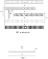
- FIG. 7 is a cross-sectional structural view of a display in one embodiment of the present disclosure.
- the main objective of the present disclosure is as follows: at least one metal layer is added to make contact with a first metal layer of an existing GOA circuit and to at least partially overlap with a second metal layer and/or poly-silicon layer of the existing GOA circuit in an insulated manner to form a capacitor, which means that at least one capacitor in series connection with the existing capacitors is added based on the existing capacitors, so that the final capacitance of the GOA circuit may be increased, but the capacitor area of the GOA circuit may be still the area of one capacitor, namely, the capacitance may be increased without enlarging the capacitor area, in other words, the capacitor area may be reduced without decreasing the capacitance, thus, facilitating the narrow-border design of LCDs.
- FIG. 1 is a cross-sectional structural view of a display panel in the first embodiment of the present disclosure.
- the display panel may be a liquid crystal display panel 10 ; however, the display panel may also be of other types, and the present disclosure has no specific limitation in this regard.
- the liquid crystal display panel 10 may include a color filter substrate (called a CF substrate for short) 11 , an array substrate (or a thin film transistor substrate called a TFT substrate for short) 12 , and liquid crystals (liquid crystal molecules) 13 filling the space between the two substrates.
- the liquid crystals 13 are located in a liquid crystal cell formed after the array substrate 12 and the color filter substrate 11 may be stacked together.
- the array substrate 12 may include a plurality of data lines 121 arrayed in a column direction, a plurality of scan lines 122 arrayed in a row direction and a plurality of pixel regions 123 defined by the scan lines 122 and the data lines 121 .
- Each pixel region 123 may be connected to one corresponding data line 121 and one corresponding scan line 122 , the scan lines 122 may be connected to a gate driver 21 to provide a scan voltage for the pixel regions 123 , and the data lines 121 may be connected to a source driver 22 to provide a grayscale voltage for the pixel regions 123 ; and a GOA circuit may be disposed in the gate driver 21 .
- the GOA circuit may include a plurality of structural layers sequentially stacked on the array substrate 12 , and the structural layers may include a poly-silicon layer 31 , a first insulation layer 32 , a first metal layer M 1 , a second insulation layer 33 , a second metal layer M 2 , a third insulation layer 34 and a third metal layer M 3 .
- the poly-silicon layer 31 may be synchronously formed with a poly-silicon semiconductor layer of a TFT of the array substrate 12 , similarly, the first metal layer M 1 may be synchronously formed with a gate electrode of the TFT, the second metal layer M 2 may be synchronously formed with a source electrode (or drain electrode) of the TFT, and the third metal layer M 3 may be synchronously formed with a common electrode layer or a pixel electrode layer of the array substrate 12 . Furthermore, the synchronously-formed structural layers may be made from the same material through the same process.
- a first via hole 124 penetrating through the second insulation layer 33 and the first insulation layer 32 and a second via hole 125 penetrating through the third insulation layer 34 and the second insulation layer 33 may be defined on the array substrate 12 .
- the second metal layer M 2 may be connected to the first metal layer M 1 through the first via hole 124 .
- the third metal layer M 3 may be connected to the first metal layer M 1 through the second via hole 125 .
- the first metal layer M 1 at least partially may overlap with the poly-silicon layer 31 , and overlapping parts of the first metal layer M 1 and the poly-silicon layer 31 may be insulated by the first insulation layer 32 clamped between the first metal layer M 1 and the poly-silicon layer 31 , so that a first capacitor C 1 may be formed.
- the second metal layer M 2 at least partially may overlap with the first metal layer M 1 , and the overlapping parts of the second metal layer M 2 and the first metal layer M 1 may be insulated by the second insulation layer 33 clamped between the second metal layer M 2 and the first metal layer M 1 , so that a second capacitor C 2 may be formed.
- the third metal layer M 3 at least partially may overlap with the second metal layer M 2 , and the overlapping parts of the third metal layer M 3 and the second metal layer M 2 may be insulated by the third insulation layer 34 clamped between the third metal layer M 3 and the second metal layer M 2 , so that a third capacitor C 3 may be formed.
- the second metal layer M 2 may make a contact with the poly-silicon layer 31 and the third metal layer M 3 may make a contact with the first metal layer M 1
- the first capacitor C 1 , the second capacitor C 2 and the third capacitor C 3 may be sequentially connected in series.
- the final capacitance of the GOA circuit may be the sum of the capacitance of the first capacitor C 1 , the capacitance of the second capacitor C 2 and the capacitance of the third capacitor C 3 ; however, the capacitor area of the GOA circuit may be the area of only one capacitor (original capacitor).
- the present disclosure may increase the capacitance without enlarging the capacitor area, which means that the present disclosure may reduce the capacitor area without decreasing the capacitance, and thus, the narrow-border design of LCDs (Liquid Crystal Displays) may be facilitated.
- the second metal layer M 2 makes a contact with the poly-silicon layer 31 , as shown in FIG. 4 .
- identical reference signals may be used to represent structural elements with identical names in the present disclosure.
- the third metal layer M 3 may not make a contact with the first metal layer M 1 .
- the GOA circuit in the related art has the same capacitor area with the GOA circuit of the present disclosure, but the GOA circuit in the related art only may include a first capacitor C 1 and a second capacitor C 2 , and thus, the total capacity of the two capacitors may be smaller than the total capacity of the three capacitors in the present disclosure.
- the first insulation layer 32 may be a gate insulation layer (GI) of the TFT
- the second insulation layer 33 may be an interlayer dielectric isolation (ILD) of the TFT.
- the common electrode layer may be located between the pixel electrode layer and the source/drain electrode (layer).
- a pas sivation layer prepared from, for instance, silicon nitride (SiN x ) and having a thickness of 100 nm may be disposed between the common electrode layer and the pixel electrode layer.
- the third insulation layer 34 may include a planarization layer (PLN) and the passivation layer of the TFT.
- the planarization layer between the third metal layer M 3 and the second metal layer M 2 may be etched away, and only the passivation layer may be reserved, in the present disclosure.
- FIG. 5 is a structural view of the second embodiment of the GOA circuit in the present disclosure.
- the GOA circuit in this embodiment further may include a fourth insulation layer 30 and a fourth metal layer M 0 , that is to say, the GOA circuit in this embodiment may include five conductive layers, namely the poly-silicon layer 31 , the first metal layer M 1 , the second metal layer M 2 , the third metal layer M 3 and the fourth metal layer M 0 .
- the fourth metal layer M 0 may be located under the poly-silicon layer 31
- the fourth insulation layer 30 may be located between the fourth metal layer M 0 and the poly-silicon layer 31 .
- the fourth metal layer M 0 may be synchronously formed with a light shield (LS) of the array substrate 12 , and the light shield may be located under the poly-silicon semiconductor layer in the TFT and is used to prevent light leakage.
- LS light shield
- a third via hole 126 penetrating through the first insulation layer 32 and the fourth insulation layer 30 may be defined on the array substrate 12 .
- the first metal layer M 1 may be connected to the fourth metal layer M 0 through the third via hole 126 .
- the poly-silicon layer 31 at least partially may overlap with the fourth metal layer M 0 , and the overlapping parts of the poly-silicon layer 31 and the fourth metal layer M 0 may be insulated by the fourth insulation layer 30 located between the poly-silicon layer 31 and the fourth metal layer M 0 , so that a fourth capacitor C 4 may be formed.
- the first metal layer M 1 may make a contact with the fourth metal layer M 0
- the fourth capacitor C 4 , the first capacitor C 1 , the second capacitor C 2 and the third capacitor C 3 may be sequentially connected in series.
- the final capacitance of the GOA circuit may be the sum of the capacitance of the first capacitor C 1 , the capacitance of the second capacitor C 2 , the capacitance of the third capacitor C 3 and the capacitance of the fourth capacitor C 4 , but the capacitor area of the GOA circuit is the area of only one capacitor.
- this embodiment may also increase the capacitance without enlarging the capacitor area, which means that this embodiment may also reduce the capacitor area without decreasing the capacitance, and thus, the narrow-border design of LCDs may be facilitated.
- an array substrate 12 shown in FIG. 5 , provided with the five conductive layers (namely the fourth metal layer M 0 , the poly-silicon layer 31 , the first metal layer M 1 , the second metal layer M 2 and the third metal layer M 3 ) in the related art, only the second metal layer M 2 makes a contact with the poly-silicon layer 31 , as shown in FIG. 6 .
- identical reference signs may be used to represent structural elements with identical names in the present disclosure.
- the third metal layer M 3 may not make a contact with the first metal layer M 1
- the poly-silicon layer 31 may not make a contact with the fourth metal layer M 0 either. Referring to FIG. 5 and FIG.
- the GOA circuit in the related art has the same capacitor area with the GOA circuit of the present disclosure, but the GOA circuit in the related art only includes a first capacitor C 1 and a second capacitor C 2 , and thus, the total capacity of the two capacitors may be smaller than the total capacity of the four capacitors in the present disclosure.
- the GOA circuit in the present disclosure may also be provided with the fourth metal layer M 0 , but may not be provided with the third metal layer M 3 .
- the final capacitance of the GOA circuit may be the sum of the capacitance of the first capacitor C 1 , the capacitance of the second capacitor C 2 and the capacitance of the fourth capacitor C 4 , but the capacitor area of the GOA circuit may be the area of the only original capacitor, so that this embodiment may also increase the capacitance without enlarging the capacitor area, which means that this embodiment may also reduce the capacitor area without decreasing the capacitance, and thus, the narrow-border design of LCDs may be facilitated.
- the present disclosure further provides a display shown in FIG. 7 .
- the display may be a liquid crystal display 70 .
- the display may also be of other types, and the present disclosure has no specific limitation in this regard.
- the liquid crystal display 70 may include the liquid crystal display panel 10 mentioned above and a backlight module 71 used to provide light for the liquid crystal display panel 10 .
- the liquid crystal display 70 may adopt the array substrate 12 designed in the aforesaid manner, thereby having identical beneficial effects.
Landscapes
- Physics & Mathematics (AREA)
- Engineering & Computer Science (AREA)
- Nonlinear Science (AREA)
- General Physics & Mathematics (AREA)
- Chemical & Material Sciences (AREA)
- Crystallography & Structural Chemistry (AREA)
- Microelectronics & Electronic Packaging (AREA)
- Mathematical Physics (AREA)
- Optics & Photonics (AREA)
- Theoretical Computer Science (AREA)
- Computer Hardware Design (AREA)
- Power Engineering (AREA)
- Devices For Indicating Variable Information By Combining Individual Elements (AREA)
- Liquid Crystal (AREA)
Abstract
Description
Claims (15)
Applications Claiming Priority (4)
| Application Number | Priority Date | Filing Date | Title |
|---|---|---|---|
| CN201810523886.6 | 2018-05-28 | ||
| CN201810523886 | 2018-05-28 | ||
| CN201810523886.6A CN108761939A (en) | 2018-05-28 | 2018-05-28 | Array substrate, display panel and display |
| PCT/CN2018/107591 WO2019227800A1 (en) | 2018-05-28 | 2018-09-26 | Array substrate, display panel, and display |
Related Parent Applications (1)
| Application Number | Title | Priority Date | Filing Date |
|---|---|---|---|
| PCT/CN2018/107591 Continuation WO2019227800A1 (en) | 2018-05-28 | 2018-09-26 | Array substrate, display panel, and display |
Publications (2)
| Publication Number | Publication Date |
|---|---|
| US20190361305A1 US20190361305A1 (en) | 2019-11-28 |
| US10690978B2 true US10690978B2 (en) | 2020-06-23 |
Family
ID=68613670
Family Applications (1)
| Application Number | Title | Priority Date | Filing Date |
|---|---|---|---|
| US16/208,514 Expired - Fee Related US10690978B2 (en) | 2018-05-28 | 2018-12-03 | Array substrate, display panel, and display |
Country Status (1)
| Country | Link |
|---|---|
| US (1) | US10690978B2 (en) |
Families Citing this family (1)
| Publication number | Priority date | Publication date | Assignee | Title |
|---|---|---|---|---|
| TW202032226A (en) * | 2020-01-14 | 2020-09-01 | 友達光電股份有限公司 | Structure of flexible circuits |
Citations (14)
| Publication number | Priority date | Publication date | Assignee | Title |
|---|---|---|---|---|
| US5499123A (en) | 1992-10-27 | 1996-03-12 | Nec Corporation | Active matrix liquid crystal display cell with light blocking capacitor electrode above insulating layer |
| CN104536637A (en) | 2015-01-29 | 2015-04-22 | 京东方科技集团股份有限公司 | Embedded touch screen and display device |
| CN104793401A (en) | 2015-05-08 | 2015-07-22 | 上海天马微电子有限公司 | Display panel and electronic equipment |
| CN204667365U (en) | 2015-06-05 | 2015-09-23 | 上海天马微电子有限公司 | Embedded self-contained touch array, substrate and test fixture |
| CN104965622A (en) | 2015-04-01 | 2015-10-07 | 上海天马微电子有限公司 | Array substrate and display panel |
| US20160293643A1 (en) | 2015-04-03 | 2016-10-06 | Apple Inc. | Display With Semiconducting Oxide and Polysilicon Transistors |
| CN106200167A (en) | 2016-08-25 | 2016-12-07 | 武汉华星光电技术有限公司 | Array base palte and liquid crystal display |
| US20160358949A1 (en) * | 2015-06-04 | 2016-12-08 | Boe Technology Group Co., Ltd. | Goa unit, method for manufacturing goa unit, display substrate and display device |
| CN106526997A (en) | 2016-12-02 | 2017-03-22 | 厦门天马微电子有限公司 | Array substrate, display panel and display device |
| US20170103720A1 (en) * | 2015-10-12 | 2017-04-13 | Century Technology (Shenzhen) Corporation Limited | Protection of gate driver on panel of thin film transistor array substrate |
| CN107527599A (en) | 2017-08-16 | 2017-12-29 | 深圳市华星光电半导体显示技术有限公司 | Scan drive circuit, array base palte and display panel |
| US20180040600A1 (en) | 2015-12-07 | 2018-02-08 | Wuhan China Star Optoelectronics Technology Co., Ltd. | Goa circuit based on ltps semiconductor thin film transistor |
| CN107785399A (en) | 2017-10-26 | 2018-03-09 | 武汉天马微电子有限公司 | A display panel and a display device |
| CN108020971A (en) * | 2017-12-22 | 2018-05-11 | 武汉华星光电技术有限公司 | Array base palte, liquid crystal panel and liquid crystal display device |
-
2018
- 2018-12-03 US US16/208,514 patent/US10690978B2/en not_active Expired - Fee Related
Patent Citations (14)
| Publication number | Priority date | Publication date | Assignee | Title |
|---|---|---|---|---|
| US5499123A (en) | 1992-10-27 | 1996-03-12 | Nec Corporation | Active matrix liquid crystal display cell with light blocking capacitor electrode above insulating layer |
| CN104536637A (en) | 2015-01-29 | 2015-04-22 | 京东方科技集团股份有限公司 | Embedded touch screen and display device |
| CN104965622A (en) | 2015-04-01 | 2015-10-07 | 上海天马微电子有限公司 | Array substrate and display panel |
| US20160293643A1 (en) | 2015-04-03 | 2016-10-06 | Apple Inc. | Display With Semiconducting Oxide and Polysilicon Transistors |
| CN104793401A (en) | 2015-05-08 | 2015-07-22 | 上海天马微电子有限公司 | Display panel and electronic equipment |
| US20160358949A1 (en) * | 2015-06-04 | 2016-12-08 | Boe Technology Group Co., Ltd. | Goa unit, method for manufacturing goa unit, display substrate and display device |
| CN204667365U (en) | 2015-06-05 | 2015-09-23 | 上海天马微电子有限公司 | Embedded self-contained touch array, substrate and test fixture |
| US20170103720A1 (en) * | 2015-10-12 | 2017-04-13 | Century Technology (Shenzhen) Corporation Limited | Protection of gate driver on panel of thin film transistor array substrate |
| US20180040600A1 (en) | 2015-12-07 | 2018-02-08 | Wuhan China Star Optoelectronics Technology Co., Ltd. | Goa circuit based on ltps semiconductor thin film transistor |
| CN106200167A (en) | 2016-08-25 | 2016-12-07 | 武汉华星光电技术有限公司 | Array base palte and liquid crystal display |
| CN106526997A (en) | 2016-12-02 | 2017-03-22 | 厦门天马微电子有限公司 | Array substrate, display panel and display device |
| CN107527599A (en) | 2017-08-16 | 2017-12-29 | 深圳市华星光电半导体显示技术有限公司 | Scan drive circuit, array base palte and display panel |
| CN107785399A (en) | 2017-10-26 | 2018-03-09 | 武汉天马微电子有限公司 | A display panel and a display device |
| CN108020971A (en) * | 2017-12-22 | 2018-05-11 | 武汉华星光电技术有限公司 | Array base palte, liquid crystal panel and liquid crystal display device |
Non-Patent Citations (1)
| Title |
|---|
| 2nd Office Action of counterpart Chinese Patent Application No. 201810523886.6 dated Oct. 28, 2019. |
Also Published As
| Publication number | Publication date |
|---|---|
| US20190361305A1 (en) | 2019-11-28 |
Similar Documents
| Publication | Publication Date | Title |
|---|---|---|
| US9116400B2 (en) | Liquid crystal display having minimized bezel area | |
| US10324348B2 (en) | Array substrate, liquid crystal display panel and liquid crystal display device | |
| US8946719B2 (en) | TFT, shift register, scan signal line driving circuit, display device, and TFT trimming method | |
| US10120249B2 (en) | Array substrate, liquid crystal display panel and liquid crystal display device | |
| CN101706637B (en) | Pixel electrode structure with high display quality | |
| US7894034B2 (en) | Thin film transistor array panel with improved connection to test lines having auxiliary test line with plural extending conductive layers in contact with at least one test line | |
| US10168593B2 (en) | Liquid crystal display panel having dual capacitors connected in parallel to shift register unit and array substrate thereof | |
| US20160307937A1 (en) | Thin-film transistor, array substrate and display apparatus | |
| US20130075766A1 (en) | Thin film transistor device and pixel structure and driving circuit of a display panel | |
| EP3282312B1 (en) | Array substrate and driving method therefor, and display device | |
| WO2017020334A1 (en) | Array substrate, liquid crystal display panel and liquid crystal display device thereof | |
| WO2019227800A1 (en) | Array substrate, display panel, and display | |
| CN102364390B (en) | Liquid crystal display (LCD) panel and method for forming same | |
| CN113406832B (en) | TFT array substrate and driving method thereof | |
| US8445335B2 (en) | Method of forming pixel structure | |
| US9666611B2 (en) | Thin film transistor array panel | |
| WO2020015175A1 (en) | Pixel driving circuit and liquid crystal display device | |
| US10690978B2 (en) | Array substrate, display panel, and display | |
| US20130100005A1 (en) | LCD Panel and Method of Manufacturing the Same | |
| US20090152730A1 (en) | Interconnected structure for TFT-array substrate | |
| US20230176435A1 (en) | Thin film transistor array substrate and touch display panel | |
| US20210150956A1 (en) | Display panel and display device | |
| US11947229B2 (en) | Display panel and display device | |
| WO2025118355A1 (en) | Array substrate and display panel | |
| TW202431620A (en) | Pixel structure |
Legal Events
| Date | Code | Title | Description |
|---|---|---|---|
| FEPP | Fee payment procedure |
Free format text: ENTITY STATUS SET TO UNDISCOUNTED (ORIGINAL EVENT CODE: BIG.); ENTITY STATUS OF PATENT OWNER: LARGE ENTITY |
|
| AS | Assignment |
Owner name: WUHAN CHINA STAR OPTOELECTRONICS TECHNOLOGY CO., L Free format text: ASSIGNMENT OF ASSIGNORS INTEREST;ASSIGNORS:HAN, YUEBAI;CHENG, LU;REEL/FRAME:047664/0078 Effective date: 20181029 Owner name: WUHAN CHINA STAR OPTOELECTRONICS TECHNOLOGY CO., LTD., CHINA Free format text: ASSIGNMENT OF ASSIGNORS INTEREST;ASSIGNORS:HAN, YUEBAI;CHENG, LU;REEL/FRAME:047664/0078 Effective date: 20181029 |
|
| STPP | Information on status: patent application and granting procedure in general |
Free format text: NON FINAL ACTION MAILED |
|
| STPP | Information on status: patent application and granting procedure in general |
Free format text: RESPONSE TO NON-FINAL OFFICE ACTION ENTERED AND FORWARDED TO EXAMINER |
|
| STPP | Information on status: patent application and granting procedure in general |
Free format text: NOTICE OF ALLOWANCE MAILED -- APPLICATION RECEIVED IN OFFICE OF PUBLICATIONS |
|
| STPP | Information on status: patent application and granting procedure in general |
Free format text: PUBLICATIONS -- ISSUE FEE PAYMENT VERIFIED |
|
| STCF | Information on status: patent grant |
Free format text: PATENTED CASE |
|
| FEPP | Fee payment procedure |
Free format text: MAINTENANCE FEE REMINDER MAILED (ORIGINAL EVENT CODE: REM.); ENTITY STATUS OF PATENT OWNER: LARGE ENTITY |
|
| LAPS | Lapse for failure to pay maintenance fees |
Free format text: PATENT EXPIRED FOR FAILURE TO PAY MAINTENANCE FEES (ORIGINAL EVENT CODE: EXP.); ENTITY STATUS OF PATENT OWNER: LARGE ENTITY |
|
| STCH | Information on status: patent discontinuation |
Free format text: PATENT EXPIRED DUE TO NONPAYMENT OF MAINTENANCE FEES UNDER 37 CFR 1.362 |
|
| FP | Lapsed due to failure to pay maintenance fee |
Effective date: 20240623 |