US10690956B2 - Liquid crystal display device comprising a transparent reinforcement plate disposed between a first polarizer and a backlight unit - Google Patents
Liquid crystal display device comprising a transparent reinforcement plate disposed between a first polarizer and a backlight unit Download PDFInfo
- Publication number
- US10690956B2 US10690956B2 US15/695,711 US201715695711A US10690956B2 US 10690956 B2 US10690956 B2 US 10690956B2 US 201715695711 A US201715695711 A US 201715695711A US 10690956 B2 US10690956 B2 US 10690956B2
- Authority
- US
- United States
- Prior art keywords
- liquid crystal
- polarizer
- reinforcement plate
- transparent
- display device
- Prior art date
- Legal status (The legal status is an assumption and is not a legal conclusion. Google has not performed a legal analysis and makes no representation as to the accuracy of the status listed.)
- Active, expires
Links
- 239000004973 liquid crystal related substance Substances 0.000 title claims abstract description 212
- 230000002787 reinforcement Effects 0.000 title claims abstract description 104
- 210000002858 crystal cell Anatomy 0.000 claims abstract description 140
- 239000000758 substrate Substances 0.000 claims abstract description 51
- 239000000853 adhesive Substances 0.000 claims description 16
- 230000001070 adhesive effect Effects 0.000 claims description 16
- 239000010410 layer Substances 0.000 claims description 15
- 229910052751 metal Inorganic materials 0.000 claims description 9
- 239000002184 metal Substances 0.000 claims description 9
- 239000005357 flat glass Substances 0.000 claims description 8
- 238000000034 method Methods 0.000 claims description 7
- 239000012790 adhesive layer Substances 0.000 claims description 5
- 230000000052 comparative effect Effects 0.000 description 9
- 239000002096 quantum dot Substances 0.000 description 8
- 239000010408 film Substances 0.000 description 7
- 239000000463 material Substances 0.000 description 7
- 239000011521 glass Substances 0.000 description 5
- 230000003287 optical effect Effects 0.000 description 5
- 230000036961 partial effect Effects 0.000 description 4
- RYGMFSIKBFXOCR-UHFFFAOYSA-N Copper Chemical compound [Cu] RYGMFSIKBFXOCR-UHFFFAOYSA-N 0.000 description 3
- OAICVXFJPJFONN-UHFFFAOYSA-N Phosphorus Chemical compound [P] OAICVXFJPJFONN-UHFFFAOYSA-N 0.000 description 3
- 229910052802 copper Inorganic materials 0.000 description 3
- 239000010949 copper Substances 0.000 description 3
- 230000002401 inhibitory effect Effects 0.000 description 3
- 239000011347 resin Substances 0.000 description 3
- 229920005989 resin Polymers 0.000 description 3
- 229910052782 aluminium Inorganic materials 0.000 description 2
- XAGFODPZIPBFFR-UHFFFAOYSA-N aluminium Chemical compound [Al] XAGFODPZIPBFFR-UHFFFAOYSA-N 0.000 description 2
- 230000008602 contraction Effects 0.000 description 2
- 230000005484 gravity Effects 0.000 description 2
- 230000000670 limiting effect Effects 0.000 description 2
- 239000007769 metal material Substances 0.000 description 2
- 238000012986 modification Methods 0.000 description 2
- 230000004048 modification Effects 0.000 description 2
- 239000004698 Polyethylene Substances 0.000 description 1
- 238000010521 absorption reaction Methods 0.000 description 1
- 230000000903 blocking effect Effects 0.000 description 1
- 239000000805 composite resin Substances 0.000 description 1
- 230000006378 damage Effects 0.000 description 1
- 230000007547 defect Effects 0.000 description 1
- 230000006866 deterioration Effects 0.000 description 1
- 238000009792 diffusion process Methods 0.000 description 1
- 239000000428 dust Substances 0.000 description 1
- 230000000694 effects Effects 0.000 description 1
- 239000006260 foam Substances 0.000 description 1
- 230000008595 infiltration Effects 0.000 description 1
- 238000001764 infiltration Methods 0.000 description 1
- 239000011159 matrix material Substances 0.000 description 1
- 238000000465 moulding Methods 0.000 description 1
- 239000012788 optical film Substances 0.000 description 1
- -1 polyethylene Polymers 0.000 description 1
- 229920000573 polyethylene Polymers 0.000 description 1
- 238000009877 rendering Methods 0.000 description 1
- 230000000979 retarding effect Effects 0.000 description 1
- 230000035939 shock Effects 0.000 description 1
- 125000006850 spacer group Chemical group 0.000 description 1
- 239000010409 thin film Substances 0.000 description 1
- 239000005341 toughened glass Substances 0.000 description 1
Images


Classifications
-
- G—PHYSICS
- G02—OPTICS
- G02F—OPTICAL DEVICES OR ARRANGEMENTS FOR THE CONTROL OF LIGHT BY MODIFICATION OF THE OPTICAL PROPERTIES OF THE MEDIA OF THE ELEMENTS INVOLVED THEREIN; NON-LINEAR OPTICS; FREQUENCY-CHANGING OF LIGHT; OPTICAL LOGIC ELEMENTS; OPTICAL ANALOGUE/DIGITAL CONVERTERS
- G02F1/00—Devices or arrangements for the control of the intensity, colour, phase, polarisation or direction of light arriving from an independent light source, e.g. switching, gating or modulating; Non-linear optics
- G02F1/01—Devices or arrangements for the control of the intensity, colour, phase, polarisation or direction of light arriving from an independent light source, e.g. switching, gating or modulating; Non-linear optics for the control of the intensity, phase, polarisation or colour
- G02F1/13—Devices or arrangements for the control of the intensity, colour, phase, polarisation or direction of light arriving from an independent light source, e.g. switching, gating or modulating; Non-linear optics for the control of the intensity, phase, polarisation or colour based on liquid crystals, e.g. single liquid crystal display cells
- G02F1/133—Constructional arrangements; Operation of liquid crystal cells; Circuit arrangements
- G02F1/1333—Constructional arrangements; Manufacturing methods
- G02F1/1335—Structural association of cells with optical devices, e.g. polarisers or reflectors
- G02F1/133528—Polarisers
-
- G—PHYSICS
- G02—OPTICS
- G02F—OPTICAL DEVICES OR ARRANGEMENTS FOR THE CONTROL OF LIGHT BY MODIFICATION OF THE OPTICAL PROPERTIES OF THE MEDIA OF THE ELEMENTS INVOLVED THEREIN; NON-LINEAR OPTICS; FREQUENCY-CHANGING OF LIGHT; OPTICAL LOGIC ELEMENTS; OPTICAL ANALOGUE/DIGITAL CONVERTERS
- G02F1/00—Devices or arrangements for the control of the intensity, colour, phase, polarisation or direction of light arriving from an independent light source, e.g. switching, gating or modulating; Non-linear optics
- G02F1/01—Devices or arrangements for the control of the intensity, colour, phase, polarisation or direction of light arriving from an independent light source, e.g. switching, gating or modulating; Non-linear optics for the control of the intensity, phase, polarisation or colour
- G02F1/13—Devices or arrangements for the control of the intensity, colour, phase, polarisation or direction of light arriving from an independent light source, e.g. switching, gating or modulating; Non-linear optics for the control of the intensity, phase, polarisation or colour based on liquid crystals, e.g. single liquid crystal display cells
- G02F1/133—Constructional arrangements; Operation of liquid crystal cells; Circuit arrangements
- G02F1/1333—Constructional arrangements; Manufacturing methods
- G02F1/133308—Support structures for LCD panels, e.g. frames or bezels
- G02F1/133317—Intermediate frames, e.g. between backlight housing and front frame
-
- G02F2001/133317—
-
- G—PHYSICS
- G02—OPTICS
- G02F—OPTICAL DEVICES OR ARRANGEMENTS FOR THE CONTROL OF LIGHT BY MODIFICATION OF THE OPTICAL PROPERTIES OF THE MEDIA OF THE ELEMENTS INVOLVED THEREIN; NON-LINEAR OPTICS; FREQUENCY-CHANGING OF LIGHT; OPTICAL LOGIC ELEMENTS; OPTICAL ANALOGUE/DIGITAL CONVERTERS
- G02F2201/00—Constructional arrangements not provided for in groups G02F1/00 - G02F7/00
- G02F2201/54—Arrangements for reducing warping-twist
Definitions
- the present disclosure relates to a liquid crystal display device.
- Liquid crystal display devices are used as, for example, displays in, for example, televisions and monitors due to their capability to display images with low power consumption.
- Such a liquid crystal display device includes, for example, a liquid crystal cell including a liquid crystal layer interposed between a pair of transparent substrates, a backlight unit disposed behind the liquid crystal cell, and a frame that holds the liquid crystal cell and the backlight unit (for example, see Japanese Unexamined Patent Application Publication No. 2000-180819).
- the present disclosure was conceived to overcome such a problem and has an object to provide a liquid crystal display device capable of inhibiting reduction in image quality by inhibiting the liquid crystal cell from warping.
- a liquid crystal display device includes: a liquid crystal cell; a backlight unit behind the liquid crystal cell; a polarizer on a surface of the liquid crystal cell, the surface opposing the backlight unit; a transparent reinforcement plate that is between the liquid crystal cell and the backlight unit and supports the polarizer; and a middle frame including a protrusion protruding toward a space between the backlight unit and the transparent reinforcement plate.
- the transparent reinforcement plate rests on the protrusion.
- liquid crystal cell can be inhibited from warping, reduction in image quality due to warping of the liquid crystal cell can be inhibited.
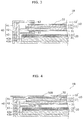
- FIG. 1 is a plan view schematically illustrating a liquid crystal display device according to an embodiment.
- FIG. 2 is a cross sectional view of the liquid crystal display device according to the embodiment, taken at line II-II in FIG. 1 .
- FIG. 3 is a partial cross sectional view of a liquid crystal display device according to comparative example 1.
- FIG. 4 is a partial cross sectional view of a liquid crystal display device according to comparative example 2.
- FIG. 1 is a plan view schematically illustrating the liquid crystal display device 1 according to the embodiment.
- FIG. 2 is a cross sectional view of the liquid crystal display device 1 according to the embodiment, taken at line II-II in FIG. 1 .
- the liquid crystal display device 1 includes a liquid crystal cell 10 , a backlight unit 20 disposed behind the liquid crystal cell 10 , a first polarizer 31 and a second polarizer 32 respectively disposed on both surfaces of the liquid crystal cell 10 , a frame 40 that holds the liquid crystal cell 10 and the backlight unit 20 , and a transparent reinforcement plate 50 .
- the liquid crystal cell 10 is a liquid crystal panel that displays an image on the display surface, which is the front surface.
- the liquid crystal cell 10 includes a pair of transparent substrates 11 and a liquid crystal layer 12 disposed between the pair of transparent substrates 11 .
- a driver substrate on which a driver integrated circuit (IC) is formed is connected to the liquid crystal cell 10 via a flexible substrate such as a flexible printed circuit (FPC).
- the liquid crystal cell 10 is, but not limited to, being driven using an in-plane switching (IPS) driving method; a vertical alignment (VA) or twisted nematic (TN) driving method may be used.
- IPS in-plane switching
- VA vertical alignment
- TN twisted nematic
- the pair of transparent substrates 11 are, for example, rectangular glass substrates disposed so as to oppose one another.
- the pair of transparent substrates 11 include a thin film transistor (TFT) substrate 11 a (TFT glass) having, for example, electric lines formed thereon, and a color filter (CF) substrate 11 b (CF glass) including red (R), green (G), and blue (B) color filters.
- TFT thin film transistor
- CF color filter
- the outline of the TFT substrate 11 a is larger than the outline of the CF substrate 11 b.
- the liquid crystal layer 12 is sealed between the pair of transparent substrates 11 .
- the liquid crystal material used for the liquid crystal layer 12 may be selected according to the method used to drive the liquid crystal cell 10 .
- the backlight unit 20 emits light toward the liquid crystal cell 10 .
- the backlight unit 20 is a surface light source that emits uniform scattered light (diffused light).
- the backlight unit 20 includes a backlight 21 and an optical sheet 22 .
- the backlight 21 is, for example, a light emitting diode (LED) backlight that uses LEDs as a light source.
- LED light emitting diode
- White LED elements that emit white light can be used as the LEDs.
- the white LED elements may include, for example, a blue LED chip and a yellow phosphor.
- the backlight 21 is a direct-lit LED backlight in which LEDs are arranged in a matrix on a substrate.
- the backlight 21 may be an edge-lit backlight including a light guide plate, a light source disposed at an edge surface of the light guide plate, and a reflector disposed on the rear surface of the light guide plate.
- the optical sheet 22 is disposed on the front surface of the backlight 21 .
- the optical sheet 22 may comprise one sheet or two or more sheets.
- the optical sheet 22 includes a diffuser (diffusion sheet) for diffusing light from the backlight 21 .
- the first polarizer 31 is disposed on the liquid crystal cell 10 , on the surface opposing the backlight unit 20 (i.e., on the rear surface of the liquid crystal cell 10 ).
- the first polarizer 31 is a lower polarizer disposed on the rear surface (lower surface) of the liquid crystal cell 10 . More specifically, the first polarizer 31 is bonded to the outer surface of the TFT substrate 11 a.
- the second polarizer 32 is disposed on the liquid crystal cell 10 , on the surface opposite the surface opposing the backlight unit 20 (i.e., on the front surface of the liquid crystal cell 10 ).
- the second polarizer 32 is an upper polarizer disposed on the front surface (upper surface) of the liquid crystal cell 10 . More specifically, the second polarizer 32 is bonded to the outer surface of the CF substrate 11 b.
- the first polarizer 31 and the second polarizer 32 are disposed such that their respective polarizing directions are orthogonal to one another. In other words, the first polarizer 31 and the second polarizer 32 are disposed in a crossed nicols configuration.
- the first polarizer 31 and the second polarizer 32 are, for example, polarizing film sheets made of a resin material.
- a phase retarder phase retarding film may be bonded to each of the first polarizer 31 and the second polarizer 32 .
- the frame 40 includes an upper frame 41 (front frame) a lower frame 42 (rear frame), and an intermediate frame 43 (middle frame).
- the upper frame 41 has a frame-like rectangular shape in a plan view, and as illustrated in FIG. 2 , is an angled component having an L-shaped cross section.
- the upper frame 41 includes a side wall disposed on a lateral side of the liquid crystal cell 10 and the backlight unit 20 , and a bezel that covers the outer periphery of the liquid crystal cell 10 .
- the upper frame 41 is an outer component that forms the outer contour of the frame 40 , and may be made of a rigid material, such as a copper or aluminum plate.
- the lower frame 42 includes a side wall that is disposed on a lateral side of the liquid crystal cell 10 and backlight unit 20 and inward relative to the side wall of the upper frame 41 , and a rear surface section that covers the lower surface of the backlight unit 20 .
- the lower frame 42 is an outer component that forms the outer contour of the frame 40 , and like the upper frame 41 , may be made of a rigid material, such as a copper or aluminum plate.
- the intermediate frame 43 has a rectangular frame-like plan view shape, and has a T-shaped cross section.
- a molded frame formed by molding composite resin may be used as the intermediate frame 43 , but the material of the intermediate frame 43 is not limited to a resin material; the intermediate frame 83 may be made of a metal material.
- the intermediate frame 43 may have light blocking properties, such as by being black in color, but is not limited to this example.
- the intermediate frame 43 includes a protrusion 43 a that protrudes toward a space between the backlight unit 20 and the transparent reinforcement plate 50 , and a side wall 43 b disposed on a lateral side of the liquid crystal cell 10 and the backlight unit 20 .
- the protrusion 43 a protrudes from the side wall 43 b , toward a space between the liquid crystal cell 10 and the transparent reinforcement plate 50 , to a position corresponding to the outer periphery of the liquid crystal cell 10 .
- the side wall 43 b is disposed between a side wall of the lower frame 42 (or upper frame 41 ) and the transparent reinforcement plate 50 . Moreover, the side wall 43 b may also function as a spacer that regulates the distance between the upper frame 41 and the lower frame 42 . The bottom end of the side wall 43 b may or may not contact the inner surface of the rear surface section of the lower frame 42 . Moreover, the top end of the side wall 43 b may or may not contact the inner surface of the bezel of the upper frame 41 .
- the transparent reinforcement plate 50 contacts the inner surface of the side wall 43 b , but the side wall 43 b and the transparent reinforcement plate 50 need not be in contact.
- the transparent reinforcement plate 50 is a support component that supports the first polarizer 31 , and is disposed between the liquid crystal cell 10 and the backlight unit 20 .
- the transparent reinforcement plate 50 is disposed between the first polarizer 31 on the liquid crystal cell 10 and the backlight unit 20 .
- the transparent reinforcement plate 50 is bonded to the first polarizer 31 on the liquid crystal cell 10 . Accordingly, the transparent reinforcement plate 50 supports the liquid crystal cell 10 in addition to the first polarizer 31 .
- the transparent reinforcement plate 50 is bonded to the first polarizer 31 via an adhesive layer 33 , which fixes the transparent reinforcement plate 50 and the liquid crystal cell 10 together.
- a transparent adhesive such as an optically clear adhesive (OCA) can be used as the adhesive layer 33 .
- the transparent reinforcement plate 50 rests on the protrusion 43 a of the intermediate frame 43 . More specifically, the transparent reinforcement plate 50 rests on the protrusion 43 a in a state in which the liquid crystal cell 10 is bonded to the transparent reinforcement plate 50 . In this case, the transparent reinforcement plate 50 is not fixed to the protrusion 43 a (the intermediate frame 43 ), but rests on the protrusion 43 a so as to be movable relative to the frame 40 . More specifically, the transparent reinforcement plate 50 rests on the protrusion 43 a such that it can freely slide horizontally relative to the surface of the liquid crystal cell 10 (i.e., parallel to the surface of the liquid crystal cell 10 ) on the frame 40 . In other words, the liquid crystal cell 10 is held by the frame 40 so as to be capable of sliding along with the transparent reinforcement plate 50 , in directions parallel to its surface.
- the transparent reinforcement plate 50 rests on the protrusion 43 a via a non-adhesive cushion 61 .
- the transparent reinforcement plate 50 is disposed on the non-adhesive cushion 61 .
- the non-adhesive cushion 61 is a shock absorbing component having a closed-cell structure, such as polyethylene foam, and the surface of the non-adhesive cushion 61 is smooth and dry to the touch.
- the non-adhesive cushion 61 is fixed to the protrusion 43 a of the intermediate frame 43 by, for example, an adhesive.
- a cushion 62 may be disposed between the upper frame 41 and the liquid crystal cell 10 . More specifically, the cushion 62 may be inserted so as to be held between the upper frame 41 and the second polarizer 32 . This makes it possible to eliminate a gap between the upper frame 41 and the liquid crystal cell 10 (the second polarizer 32 ), thereby making it possible to inhibit infiltration of, for example, dust and/or bugs.
- the outer contour of the transparent reinforcement plate 50 is external to the outer contour of the liquid crystal cell 10 .
- the outline of the transparent reinforcement plate 50 is larger than the outline of the liquid crystal cell 10 .
- the outline of the transparent reinforcement plate 50 is designed to be larger than the outline of the TFT substrate 11 a.
- the outline of the transparent reinforcement plate 50 to be larger than the outline of the liquid crystal cell 10 , as illustrated in FIG. 2 , a gap g between the inner surface of the side wall 43 b of the intermediate frame 43 and the liquid crystal cell 10 (the TFT substrate 11 a ) can be provided.
- the gap g is equivalent to the difference in size between the transparent reinforcement plate 50 and the liquid crystal cell 10 (the TFT substrate 11 a ). This prevents the liquid crystal cell 10 (the TFT substrate 11 a ) from contacting the intermediate frame 43 .
- plate glass that is transparent relative to visible light can be used as the transparent reinforcement plate 50 configured as described above. More specifically, tempered glass that has excellent mechanical strength can be used as the transparent reinforcement plate 50 . In this case, the glass used as the transparent reinforcement plate 50 may transmit infrared light in addition to visible light.
- a metal layer made of a metal material that has a high thermal conductivity, such as copper, may be formed on the transparent reinforcement plate 50 .
- a patterned film having holes arranged in a mesh or grid pattern may be used as the metal layer, or a metal film formed on almost the entire surface of the transparent reinforcement plate 50 may be used as the metal layer so long as the film is thin enough to transmit light.
- the metal layer is desirably formed on the surface of the transparent reinforcement plate 50 that opposes the backlight unit 20 .
- the liquid crystal display device 1 configured in this manner is HDR-compatible, which is compatible with, for example, 4K/8K, and as described above, a high-luminosity direct-lit LED backlight capable of local dimming is used as the backlight 21 . This makes it possible to display a high contrast, high-quality color image.
- FIG. 3 is a partial cross sectional view of a liquid crystal display device 1 A according to comparative example 1.
- FIG. 4 is a partial cross sectional view of a liquid crystal display device 1 B according to comparative example 2.
- liquid crystal display devices it is conceivable for the liquid crystal cell to be held down using a structural component such as a frame in order to fix the liquid crystal cell in place.
- a structural component such as a frame
- physically holding down the liquid crystal cell using a structural component reduces the quality of images displayed on the liquid crystal cell. For example, holding the edge portion of the liquid crystal cell down by the upper frame generates local stress in the liquid crystal cell, which reduces image quality.
- the liquid crystal cell 10 is held by the frame 40 in a state in which a gap is present (i.e., in a state in which there is clearance) between the upper frame 41 and the liquid crystal cell 10 .
- first polarizer 31 and the second polarizer 32 are respectively disposed on both surfaces of the liquid crystal cell 10 , and expansion of the first polarizer 31 and the second polarizer 32 due to heat or absorbing moisture causes the liquid crystal cell 10 to warp.
- the first polarizer 31 and the second polarizer 32 are affected by heat as a result of light from the backlight unit 20 being absorbed as it passes through the first polarizer 31 and the second polarizer 32 and converted into heat.
- the first polarizer 31 and the second polarizer 32 are also affected by heat as a result of light from the backlight unit 20 being absorbed as it passes through the liquid crystal cell 10 and converted into heat, whereby the heat produced in the liquid crystal cell 10 transfers to the first polarizer 31 and the second polarizer 32 .
- approximately 95% of the light from the backlight unit 20 is absorbed by the liquid crystal cell 10 .
- the first polarizer 31 and the second polarizer 32 thermally expand laterally.
- the amounts of thermal expansion (amounts of increase in size) of the first polarizer 31 and the second polarizer 32 are different, the liquid crystal cell 10 sandwiched between the first polarizer 31 and the second polarizer 32 warps.
- the liquid crystal cell 10 warps not only when the first polarizer 31 and the second polarizer 32 expand, but may also warp when the first polarizer 31 and the second polarizer 32 contract when, for example, the temperatures of the first polarizer 31 and the second polarizer 32 decrease.
- the liquid crystal cell 10 warping in this manner reduces the image quality of the liquid crystal display device 1 A. For example, when the liquid crystal cell 10 is driven using an IPS driving method, regions displayed in black appear uneven.
- one conceivable configuration is to include a transparent reinforcement plate 50 B that covers the entire front surface of the liquid crystal cell 10 , as illustrated in the liquid crystal display device 1 B according to comparative example 2 illustrated in FIG. 4 .
- the transparent reinforcement plate 50 B which is a single pane of plate glass, is disposed to cover the second polarizer 32 on the front surface of the liquid crystal cell 10 and the front surface of the bezel of the upper frame 41 , and is bonded to the second polarizer 32 and the upper frame 41 using a transparent adhesive.
- the liquid crystal cell 10 is fixed to the upper frame 41 via the transparent reinforcement plate 50 B, whereby the liquid crystal cell 10 is held down by the transparent reinforcement plate 50 B, thereby restricting movement of the liquid crystal cell 10 . Accordingly, there is concern that this will generate local stress in the liquid crystal cell 10 , resulting in a localized reduction of image quality. Moreover, when the liquid crystal cell 10 is fixed in place by the frame 40 (the upper frame 41 ), if the frame 40 deforms due to, for example, being screwed down or compressed, this may generate stress in the liquid crystal cell 10 and reduce image quality.
- the first polarizer 31 which is closer to the backlight unit 20 than the second polarizer 32 , is more likely to have a higher amount of thermal expansion than the second polarizer 32 .
- internal stress may generate in the substrates 11 a and 11 b in the liquid crystal cell 10 whereby double refraction may occur in the surfaces of the substrates 11 a and 11 b , possibly causing a reduction in image quality.
- the backlight unit 20 When the backlight unit 20 is capable of local dimming in particular, there is a chance that light from the backlight unit 20 may not only illuminate the liquid crystal cell 10 and the first polarizer 31 (the second polarizer 32 ) in entirety, but also locally. Accordingly, in addition to cases in which the first polarizer 31 and the second polarizer 32 expand as a whole, causing the liquid crystal cell 10 to tend to warp as a whole, there are cases in which the first polarizer 31 and the second polarizer 32 expand locally, causing the liquid crystal cell 10 to tend to warp locally. In such cases, there is concern that this will produce a localized reduction in image quality. Moreover, when the backlight unit 20 is a high-luminosity, HDR compatible backlight unit, the localized warping of the liquid crystal cell 10 is obvious.
- the liquid crystal display device 1 includes: the liquid crystal cell 10 including a pair of transparent substrates 11 and a liquid crystal layer 12 disposed between the pair of transparent substrates 11 ; the backlight unit 20 behind the liquid crystal cell 10 ; the first polarizer 31 on a surface of the liquid crystal cell 10 , the surface opposing the backlight unit 20 ; the transparent reinforcement plate 50 that is between the liquid crystal cell 10 and the backlight unit 20 and supports the first polarizer 31 ; and the intermediate frame 43 , which is the middle frame, including the protrusion 43 a protruding toward a space between the backlight unit 20 and the transparent reinforcement plate 50 .
- the transparent reinforcement plate 50 rests on the protrusion 43 a of the intermediate frame 43 .
- the first polarizer 31 on the rear surface side of the liquid crystal cell 10 is supported by the transparent reinforcement plate 50 and the transparent reinforcement plate 50 rests on the protrusion 43 a of the intermediate frame 43 .
- the transparent reinforcement plate 50 rests on the protrusion 43 a of the intermediate frame 43 , the transparent reinforcement plate 50 is held by the frame 40 in a state in which it is not fixed in the frame 40 . In other words, the transparent reinforcement plate 50 is movable relative to the frame 40 . As a result, the liquid crystal cell 10 held by the transparent reinforcement plate 50 is also held by the frame 40 without being fixed to the frame 40 . This makes it possible to inhibit reduction in image quality since generation of stress in the liquid crystal cell 10 can be inhibited even if the frame 40 deforms due to, for example, being screwed down or compressed.
- the transparent reinforcement plate 50 is disposed behind the liquid crystal cell 10 and not in front of the liquid crystal cell 10 , even when the liquid crystal display device 1 is used as a sensor panel, stray light can be inhibited from entering.
- the outer contour of the transparent reinforcement plate 50 is external to the outer contour of the liquid crystal cell 10 .
- the intermediate frame 43 is located below the liquid crystal cell 10
- the liquid crystal cell 10 and the transparent reinforcement plate 50 move downward due to gravity, but when the outer contour of the transparent reinforcement plate 50 is further inward than the outer contour of the liquid crystal cell 10 (for example, when the outline of the transparent reinforcement plate 50 is smaller than the outline of the liquid crystal cell 10 ), the liquid crystal cell 10 protrudes out farther than the transparent reinforcement plate 50 , whereby the edge of the liquid crystal cell 10 rather than the transparent reinforcement plate 50 comes into contact with the intermediate frame 43 .
- This places stress on the edge portion of the liquid crystal cell 10 and may deform the liquid crystal cell 10 and thus reduce image quality, or damage the end portion of the liquid crystal cell 10 .
- the liquid crystal display device 1 further includes the non-adhesive cushion 61 that is fixed to the protrusion 43 a of the intermediate frame 43 , and the transparent reinforcement plate 50 rests on the protrusion 43 a via the non-adhesive cushion 61 .
- a metal layer may be formed on the transparent reinforcement plate 50 .
- the transparent reinforcement plate 50 may be plate glass.
- the transparent reinforcement plate 50 may transmit infrared light in addition to visible light.
- the first polarizer 31 is affected by heat when the transparent reinforcement plate 50 absorbs infrared light, the absorbed infrared light is converted into heat, and the heat is transferred to the first polarizer 31 .
- the first polarizer 31 can be inhibited from being affected by heat resulting from the transparent reinforcement plate 50 absorbing light. This makes it possible to further inhibit the liquid crystal cell 10 from warping due to thermal expansion of the first polarizer 31 .
- the transparent reinforcement plate 50 is bonded to the first polarizer 31 via the adhesive layer 33 .
- the transparent reinforcement plate 50 and the liquid crystal cell 10 can easily be bonded together. Moreover, by bonding the transparent reinforcement plate 50 and the liquid crystal cell 10 together, the transparent reinforcement plate 50 and the liquid crystal cell 10 can move as a single unit relative to the frame 40 . With this, the transparent reinforcement plate 50 and the liquid crystal cell 10 can be held by the frame 40 as a single unit, and reduction in image quality due to deformation of the frame 40 can be inhibited.
- liquid crystal display device according to the present disclosure has been described according to an exemplary embodiment, the present disclosure is not limited to this embodiment.
- white light is produced using phosphor as a wavelength converter in the backlight unit 20 , but this example is not limiting; for example, quantum dots may be used as a wavelength converter.
- white LED elements employing quantum dots may be used as the light source for the backlight 21 , but an optical film (quantum dot film) containing quantum dots such as a quantum dot enhancement film (QDEF) may be used as the optical sheet 22 , and blue LED elements that emit blue light that excites the quantum dots may be used as the light source for the backlight 21 .
- QDEF quantum dot enhancement film
- two types of quantum dots may be used to convert the blue light into green light and red light.
- glass substrates are used as the transparent substrates 11 included in the liquid crystal cell 10 , but this example is not limiting; for example, transparent resin substrates may be used as the transparent substrates 11 .
Landscapes
- Physics & Mathematics (AREA)
- Nonlinear Science (AREA)
- Mathematical Physics (AREA)
- Chemical & Material Sciences (AREA)
- Crystallography & Structural Chemistry (AREA)
- General Physics & Mathematics (AREA)
- Optics & Photonics (AREA)
- Liquid Crystal (AREA)
- Devices For Indicating Variable Information By Combining Individual Elements (AREA)
Abstract
Description
Claims (20)
Applications Claiming Priority (2)
| Application Number | Priority Date | Filing Date | Title |
|---|---|---|---|
| JP2016-192085 | 2016-09-29 | ||
| JP2016192085A JP2018054941A (en) | 2016-09-29 | 2016-09-29 | Liquid crystal display device |
Publications (2)
| Publication Number | Publication Date |
|---|---|
| US20180088394A1 US20180088394A1 (en) | 2018-03-29 |
| US10690956B2 true US10690956B2 (en) | 2020-06-23 |
Family
ID=61686121
Family Applications (1)
| Application Number | Title | Priority Date | Filing Date |
|---|---|---|---|
| US15/695,711 Active 2037-09-15 US10690956B2 (en) | 2016-09-29 | 2017-09-05 | Liquid crystal display device comprising a transparent reinforcement plate disposed between a first polarizer and a backlight unit |
Country Status (2)
| Country | Link |
|---|---|
| US (1) | US10690956B2 (en) |
| JP (1) | JP2018054941A (en) |
Families Citing this family (6)
| Publication number | Priority date | Publication date | Assignee | Title |
|---|---|---|---|---|
| US11054684B2 (en) * | 2018-08-27 | 2021-07-06 | HKC Corporation Limited | Backlight module and display device |
| JP7221779B2 (en) | 2019-04-26 | 2023-02-14 | アルパイン株式会社 | Display device and its assembly method |
| CN110441933A (en) * | 2019-07-19 | 2019-11-12 | 武汉华星光电技术有限公司 | Display panel manufactured by the manufacturing method and use this method of display panel |
| CN111552116B (en) * | 2020-05-13 | 2022-08-30 | 深圳创维-Rgb电子有限公司 | Liquid crystal module and liquid crystal display device |
| CN111708197B (en) * | 2020-06-23 | 2023-12-26 | 北京小米移动软件有限公司 | Display device and method of making display device |
| TWI761295B (en) * | 2021-10-07 | 2022-04-11 | 達擎股份有限公司 | Display |
Citations (14)
| Publication number | Priority date | Publication date | Assignee | Title |
|---|---|---|---|---|
| US5432624A (en) * | 1993-12-03 | 1995-07-11 | Reliant Technologies, Inc. | Optical display unit in which light passes a first cell, reflects, then passes a second cell |
| JPH1124024A (en) | 1997-07-02 | 1999-01-29 | Canon Inc | Liquid crystal device |
| JP2000180819A (en) | 1998-12-16 | 2000-06-30 | Casio Comput Co Ltd | Liquid crystal display |
| JP2000347168A (en) | 1999-03-30 | 2000-12-15 | Seiko Epson Corp | Electro-optical device and projection display device provided with the same |
| US6327006B1 (en) * | 1998-10-28 | 2001-12-04 | Sony Corporation | TFT-LCD having shielding layers on TFT-substrate |
| US6414781B1 (en) | 1999-03-30 | 2002-07-02 | Seiko Epson Corporation | Electro-optical device and projection display device including the same |
| US6437846B1 (en) * | 1993-03-15 | 2002-08-20 | Seiko Epson Corporation | Liquid crystal display device and electronic device including same |
| US20040179165A1 (en) * | 2002-05-17 | 2004-09-16 | Masaki Kinoshita | Display apparatus and method of manufacturing the same |
| WO2008093704A1 (en) | 2007-01-31 | 2008-08-07 | Seiko Instruments Inc. | Display |
| JP2012093530A (en) | 2010-10-27 | 2012-05-17 | Mitsubishi Electric Corp | Display device |
| US20130107143A1 (en) * | 2011-10-31 | 2013-05-02 | Microsoft Corporation | Impact resistant construction of an interactive device |
| US20130155351A1 (en) * | 2011-12-20 | 2013-06-20 | Adam T. Garelli | Electronic Device With Backlit Display |
| US20140078444A1 (en) * | 2011-05-09 | 2014-03-20 | Sharp Kabushiki Kaisha | Panel composite body, display device and panel composite body manufacturing method |
| US20140285747A1 (en) * | 2013-03-20 | 2014-09-25 | Lg Display Co., Ltd. | Liquid crystal display with narrow bezel area |
Family Cites Families (10)
| Publication number | Priority date | Publication date | Assignee | Title |
|---|---|---|---|---|
| JPH0345585U (en) * | 1989-09-12 | 1991-04-26 | ||
| JPH09258203A (en) * | 1996-03-19 | 1997-10-03 | Hitachi Ltd | Liquid crystal display |
| KR100704741B1 (en) * | 2002-03-29 | 2007-04-11 | 도시바 마쯔시따 디스플레이 테크놀로지 컴퍼니, 리미티드 | Lighting unit and liquid crystal display using the same |
| JP2004117701A (en) * | 2002-09-25 | 2004-04-15 | Sanyo Electric Co Ltd | Multi-panel type display device |
| JP2005077590A (en) * | 2003-08-29 | 2005-03-24 | Hitachi Displays Ltd | Image display device |
| JP2005201938A (en) * | 2004-01-13 | 2005-07-28 | Mitsubishi Rayon Co Ltd | Liquid crystal display |
| KR101783671B1 (en) * | 2011-04-21 | 2017-10-10 | 엘지디스플레이 주식회사 | Liquid crystal display device |
| JP2014026173A (en) * | 2012-07-27 | 2014-02-06 | Japan Display Inc | Liquid crystal display device |
| JP2015152635A (en) * | 2014-02-10 | 2015-08-24 | シャープ株式会社 | liquid crystal display device |
| JP2017187711A (en) * | 2016-04-08 | 2017-10-12 | キヤノン株式会社 | Display device |
-
2016
- 2016-09-29 JP JP2016192085A patent/JP2018054941A/en active Pending
-
2017
- 2017-09-05 US US15/695,711 patent/US10690956B2/en active Active
Patent Citations (16)
| Publication number | Priority date | Publication date | Assignee | Title |
|---|---|---|---|---|
| US6437846B1 (en) * | 1993-03-15 | 2002-08-20 | Seiko Epson Corporation | Liquid crystal display device and electronic device including same |
| US5432624A (en) * | 1993-12-03 | 1995-07-11 | Reliant Technologies, Inc. | Optical display unit in which light passes a first cell, reflects, then passes a second cell |
| JPH1124024A (en) | 1997-07-02 | 1999-01-29 | Canon Inc | Liquid crystal device |
| US6327006B1 (en) * | 1998-10-28 | 2001-12-04 | Sony Corporation | TFT-LCD having shielding layers on TFT-substrate |
| JP2000180819A (en) | 1998-12-16 | 2000-06-30 | Casio Comput Co Ltd | Liquid crystal display |
| JP2000347168A (en) | 1999-03-30 | 2000-12-15 | Seiko Epson Corp | Electro-optical device and projection display device provided with the same |
| US6414781B1 (en) | 1999-03-30 | 2002-07-02 | Seiko Epson Corporation | Electro-optical device and projection display device including the same |
| US20020131141A1 (en) | 1999-03-30 | 2002-09-19 | Seiko Epson Corporation | Electro-optical device and projection display device including the same |
| US20040179165A1 (en) * | 2002-05-17 | 2004-09-16 | Masaki Kinoshita | Display apparatus and method of manufacturing the same |
| WO2008093704A1 (en) | 2007-01-31 | 2008-08-07 | Seiko Instruments Inc. | Display |
| US20100014034A1 (en) | 2007-01-31 | 2010-01-21 | Tsutomu Matsuhira | Display device |
| JP2012093530A (en) | 2010-10-27 | 2012-05-17 | Mitsubishi Electric Corp | Display device |
| US20140078444A1 (en) * | 2011-05-09 | 2014-03-20 | Sharp Kabushiki Kaisha | Panel composite body, display device and panel composite body manufacturing method |
| US20130107143A1 (en) * | 2011-10-31 | 2013-05-02 | Microsoft Corporation | Impact resistant construction of an interactive device |
| US20130155351A1 (en) * | 2011-12-20 | 2013-06-20 | Adam T. Garelli | Electronic Device With Backlit Display |
| US20140285747A1 (en) * | 2013-03-20 | 2014-09-25 | Lg Display Co., Ltd. | Liquid crystal display with narrow bezel area |
Also Published As
| Publication number | Publication date |
|---|---|
| JP2018054941A (en) | 2018-04-05 |
| US20180088394A1 (en) | 2018-03-29 |
Similar Documents
| Publication | Publication Date | Title |
|---|---|---|
| US10690956B2 (en) | Liquid crystal display device comprising a transparent reinforcement plate disposed between a first polarizer and a backlight unit | |
| KR102119583B1 (en) | Liquid crystal display device | |
| JP5933509B2 (en) | Liquid crystal display | |
| TWI537639B (en) | Display device | |
| KR101433705B1 (en) | Liquid crystal display device | |
| US9632237B2 (en) | Illumination device, display device, and TV receiver | |
| US9322980B2 (en) | Illumination device, display device, and television receiving device | |
| WO2015059965A1 (en) | Display device and television receiver | |
| US20140204275A1 (en) | Illumination device, display device, and television reception device | |
| KR102068959B1 (en) | Liquid crystal display device | |
| KR102078026B1 (en) | Liquid crystal display device | |
| CN106019667A (en) | Display device | |
| KR101418920B1 (en) | Backlight unit for liquid crystal display device | |
| KR102150423B1 (en) | liquid crystal display device | |
| KR20180057942A (en) | Liquid crystal display device | |
| CN107532785A (en) | Lighting device, display device and radiovisor | |
| TWI643002B (en) | Liquid crystal display device | |
| KR102260858B1 (en) | Liquid crystal display device and modularization method of LCD | |
| JP2018163315A (en) | Display | |
| KR102132767B1 (en) | Liquid crystal display device | |
| KR102047223B1 (en) | Backlight unit using LED and liquid crystal display device including the same | |
| KR102486414B1 (en) | Liquid crystal display device | |
| KR102271067B1 (en) | Liquid crystal display device | |
| KR102400219B1 (en) | Display device | |
| KR102177589B1 (en) | Liquid crystal display device |
Legal Events
| Date | Code | Title | Description |
|---|---|---|---|
| FEPP | Fee payment procedure |
Free format text: ENTITY STATUS SET TO UNDISCOUNTED (ORIGINAL EVENT CODE: BIG.); ENTITY STATUS OF PATENT OWNER: LARGE ENTITY |
|
| AS | Assignment |
Owner name: PANASONIC LIQUID CRYSTAL DISPLAY CO., LTD., JAPAN Free format text: ASSIGNMENT OF ASSIGNORS INTEREST;ASSIGNORS:NOTOSHI, TOMOHARU;YABUKI, RYOSUKE;REEL/FRAME:044415/0507 Effective date: 20170825 |
|
| STPP | Information on status: patent application and granting procedure in general |
Free format text: NON FINAL ACTION MAILED |
|
| STPP | Information on status: patent application and granting procedure in general |
Free format text: RESPONSE TO NON-FINAL OFFICE ACTION ENTERED AND FORWARDED TO EXAMINER |
|
| STPP | Information on status: patent application and granting procedure in general |
Free format text: FINAL REJECTION MAILED |
|
| STPP | Information on status: patent application and granting procedure in general |
Free format text: DOCKETED NEW CASE - READY FOR EXAMINATION |
|
| STPP | Information on status: patent application and granting procedure in general |
Free format text: NON FINAL ACTION MAILED |
|
| STPP | Information on status: patent application and granting procedure in general |
Free format text: NOTICE OF ALLOWANCE MAILED -- APPLICATION RECEIVED IN OFFICE OF PUBLICATIONS |
|
| STPP | Information on status: patent application and granting procedure in general |
Free format text: PUBLICATIONS -- ISSUE FEE PAYMENT VERIFIED |
|
| STCF | Information on status: patent grant |
Free format text: PATENTED CASE |
|
| AS | Assignment |
Owner name: PANASONIC INTELLECTUAL PROPERTY CORPORATION OF AMERICA, CALIFORNIA Free format text: ASSIGNMENT OF ASSIGNORS INTEREST;ASSIGNOR:PANASONIC LIQUID CRYSTAL DISPLAY CO., LTD.;REEL/FRAME:064292/0775 Effective date: 20230707 |
|
| MAFP | Maintenance fee payment |
Free format text: PAYMENT OF MAINTENANCE FEE, 4TH YEAR, LARGE ENTITY (ORIGINAL EVENT CODE: M1551); ENTITY STATUS OF PATENT OWNER: LARGE ENTITY Year of fee payment: 4 |