US10690710B2 - Method for preparing an object to be tested and method for improving the uniformity and intensity of an electric field induced in said object illuminated by an incident electromagnetic wave - Google Patents
Method for preparing an object to be tested and method for improving the uniformity and intensity of an electric field induced in said object illuminated by an incident electromagnetic wave Download PDFInfo
- Publication number
- US10690710B2 US10690710B2 US15/312,867 US201515312867A US10690710B2 US 10690710 B2 US10690710 B2 US 10690710B2 US 201515312867 A US201515312867 A US 201515312867A US 10690710 B2 US10690710 B2 US 10690710B2
- Authority
- US
- United States
- Prior art keywords
- cavity
- extension element
- relative permittivity
- support device
- tested
- Prior art date
- Legal status (The legal status is an assumption and is not a legal conclusion. Google has not performed a legal analysis and makes no representation as to the accuracy of the status listed.)
- Expired - Fee Related, expires
Links
- 238000000034 method Methods 0.000 title claims abstract description 39
- 230000005684 electric field Effects 0.000 title claims description 47
- 239000000463 material Substances 0.000 claims abstract description 44
- 239000004020 conductor Substances 0.000 claims description 10
- 238000005286 illumination Methods 0.000 claims description 7
- 230000008878 coupling Effects 0.000 description 9
- 238000010168 coupling process Methods 0.000 description 9
- 238000005859 coupling reaction Methods 0.000 description 9
- 229920001817 Agar Polymers 0.000 description 7
- 241000206672 Gelidium Species 0.000 description 7
- 235000010419 agar Nutrition 0.000 description 7
- 239000000523 sample Substances 0.000 description 6
- 230000008901 benefit Effects 0.000 description 4
- 230000005540 biological transmission Effects 0.000 description 4
- 230000005672 electromagnetic field Effects 0.000 description 4
- 238000002474 experimental method Methods 0.000 description 4
- 230000006872 improvement Effects 0.000 description 4
- 238000002360 preparation method Methods 0.000 description 4
- 238000004088 simulation Methods 0.000 description 4
- 239000000919 ceramic Substances 0.000 description 3
- 230000000694 effects Effects 0.000 description 3
- 239000011521 glass Substances 0.000 description 3
- 239000000126 substance Substances 0.000 description 3
- SNKAWJBJQDLSFF-NVKMUCNASA-N 1,2-dioleoyl-sn-glycero-3-phosphocholine Chemical compound CCCCCCCC\C=C/CCCCCCCC(=O)OC[C@H](COP([O-])(=O)OCC[N+](C)(C)C)OC(=O)CCCCCCC\C=C/CCCCCCCC SNKAWJBJQDLSFF-NVKMUCNASA-N 0.000 description 2
- 239000000499 gel Substances 0.000 description 2
- 239000007788 liquid Substances 0.000 description 2
- 230000002787 reinforcement Effects 0.000 description 2
- 238000004659 sterilization and disinfection Methods 0.000 description 2
- 239000000725 suspension Substances 0.000 description 2
- 241000699670 Mus sp. Species 0.000 description 1
- 206010028980 Neoplasm Diseases 0.000 description 1
- 230000009286 beneficial effect Effects 0.000 description 1
- 201000011510 cancer Diseases 0.000 description 1
- 238000012512 characterization method Methods 0.000 description 1
- 239000002131 composite material Substances 0.000 description 1
- 238000005202 decontamination Methods 0.000 description 1
- 230000003588 decontaminative effect Effects 0.000 description 1
- 230000007123 defense Effects 0.000 description 1
- 238000009826 distribution Methods 0.000 description 1
- 230000003993 interaction Effects 0.000 description 1
- 239000006193 liquid solution Substances 0.000 description 1
- 239000000203 mixture Substances 0.000 description 1
- 230000001537 neural effect Effects 0.000 description 1
- 238000009828 non-uniform distribution Methods 0.000 description 1
- 230000000149 penetrating effect Effects 0.000 description 1
- 230000008569 process Effects 0.000 description 1
- 239000013074 reference sample Substances 0.000 description 1
- 230000000638 stimulation Effects 0.000 description 1
- 230000009466 transformation Effects 0.000 description 1
- 239000002691 unilamellar liposome Substances 0.000 description 1
- 238000010200 validation analysis Methods 0.000 description 1
Images




Classifications
-
- G—PHYSICS
- G01—MEASURING; TESTING
- G01R—MEASURING ELECTRIC VARIABLES; MEASURING MAGNETIC VARIABLES
- G01R29/00—Arrangements for measuring or indicating electric quantities not covered by groups G01R19/00 - G01R27/00
- G01R29/08—Measuring electromagnetic field characteristics
- G01R29/0807—Measuring electromagnetic field characteristics characterised by the application
- G01R29/0814—Field measurements related to measuring influence on or from apparatus, components or humans, e.g. in ESD, EMI, EMC, EMP testing, measuring radiation leakage; detecting presence of micro- or radiowave emitters; dosimetry; testing shielding; measurements related to lightning
- G01R29/0821—Field measurements related to measuring influence on or from apparatus, components or humans, e.g. in ESD, EMI, EMC, EMP testing, measuring radiation leakage; detecting presence of micro- or radiowave emitters; dosimetry; testing shielding; measurements related to lightning rooms and test sites therefor, e.g. anechoic chambers, open field sites or TEM cells
- G01R29/0828—TEM-cells
-
- G—PHYSICS
- G01—MEASURING; TESTING
- G01N—INVESTIGATING OR ANALYSING MATERIALS BY DETERMINING THEIR CHEMICAL OR PHYSICAL PROPERTIES
- G01N22/00—Investigating or analysing materials by the use of microwaves or radio waves, i.e. electromagnetic waves with a wavelength of one millimetre or more
-
- G—PHYSICS
- G01—MEASURING; TESTING
- G01N—INVESTIGATING OR ANALYSING MATERIALS BY DETERMINING THEIR CHEMICAL OR PHYSICAL PROPERTIES
- G01N1/00—Sampling; Preparing specimens for investigation
- G01N1/28—Preparing specimens for investigation including physical details of (bio-)chemical methods covered elsewhere, e.g. G01N33/50, C12Q
-
- G—PHYSICS
- G01—MEASURING; TESTING
- G01N—INVESTIGATING OR ANALYSING MATERIALS BY DETERMINING THEIR CHEMICAL OR PHYSICAL PROPERTIES
- G01N1/00—Sampling; Preparing specimens for investigation
- G01N1/28—Preparing specimens for investigation including physical details of (bio-)chemical methods covered elsewhere, e.g. G01N33/50, C12Q
- G01N1/44—Sample treatment involving radiation, e.g. heat
-
- G—PHYSICS
- G01—MEASURING; TESTING
- G01N—INVESTIGATING OR ANALYSING MATERIALS BY DETERMINING THEIR CHEMICAL OR PHYSICAL PROPERTIES
- G01N33/00—Investigating or analysing materials by specific methods not covered by groups G01N1/00 - G01N31/00
- G01N33/48—Biological material, e.g. blood, urine; Haemocytometers
- G01N33/483—Physical analysis of biological material
- G01N33/4833—Physical analysis of biological material of solid biological material, e.g. tissue samples, cell cultures
Definitions
- the domain of the invention is electromagnetism and bioelectromagnetism.
- the invention is particularly applicable in the field of dosimetric characterisation of an object to be tested when this object is illuminated by an incident electromagnetic wave in free space or in an exposure system for experimental purposes, to study interactions between electromagnetic waves and living tissues.
- plane wave type exposure systems
- CRBM reverberating rooms
- wave guides cylindrical or rectangular
- wire patch cells radial transmission lines or transmission lines with plane conductors, for example such as TEM (Transverse Electro Magnetic) cells.
- TEM Transverse Electro Magnetic
- the disadvantage of these systems is that the uniformity of the incident electromagnetic field is more or less good depending on the exposure system used.
- the main purpose of the invention is to improve the uniformity and to increase the intensity of an electric field induced in an object under test exposed to an incident electric field.
- the invention discloses a method for preparation of an object to be tested that will be illuminated by an incident electromagnetic wave, the object having a given relative permittivity, wherein the method comprises:
- an extension element has a relative permittivity equal to the relative permittivity of the object within +/ ⁇ 40%, and preferably within +/ ⁇ 30%, even more preferably within +/ ⁇ 25%, even more preferably within +/ ⁇ 20% and even more preferably within +/ ⁇ 10%.
- the chosen extension elements shall have the same relative permittivity.
- the efficiency of the method according to the invention is maximum when the relative permittivity of the extension element(s) is (are) equal to that of the object and degrades with increasing difference between the relative permittivities of the object and the extension element(s).
- the relative permittivity of an extension element is equal to the relative permittivity of the object.
- the object to be tested has a given electrical conductivity and the electrical conductivity of said at least one extension element is equal to that of the object within +/ ⁇ 30%, preferably within +/ ⁇ 25%, even more preferably within +/ ⁇ 20% and even more preferably within +/ ⁇ 10%.
- the extension material is chosen to have an electrically conductivity similar to or ideally equal to that of the object.
- the extension elements chosen are made of the same material so that they will have the same relative permittivity and the same electrical conductivity.
- the part comprises a support device and said at least one extension element is a layer deposited on a surface of the support device, a well being made in said layer to form the cavity in which the object is to be housed.
- the support device might be a plate, for example a glass slide for a microscope, or a container such as a Petri box.
- said at least one extension element is a layer, a non-through well being made in said layer to form the cavity in which the object is to be housed.
- This layer may possibly be deposited on a support device (plate or Petri box).
- said at least one extension element is a block comprising a closed cavity that forms the cavity in which the object is to be housed.
- the part comprises a hollow support device with two opposite ends connected by a wall and said at least one extension element is a first layer closing off one of the two ends of the hollow support device and a second layer closing off the other one of the two ends of the hollow support device, the space delimited by the wall and the first and second layers forming the cavity in which the object is to be housed.
- the support may for example be an EppendorfTM type tube.
- the first and second layers are made of the same material.
- the cavity in which the object is to be housed in the above variants is a cylinder with a variable height (Petri box, EppendorfTM tube, etc.). Cylindrical shapes are frequently used by biologists (Petri boxes, EppendorfTM tubes, etc.).
- the cylindrical geometry of the well also has the advantage that it prevents reinforcement of fields at sharp-cornered parts that could have a less regular geometry.
- the length of an extension element on each side of the cavity is equal to at least half, and preferably equal to at least the length, and even more preferably equal to at least twice the length of the cavity along the passage direction.
- the invention also concerns a method for improving the uniformity and intensity of the electric field induced in an object to be tested illuminated by an electromagnetic wave, said method comprising:
- the improvement method according to the invention may be used in free space.
- the preparation step of the object to be tested further includes placement of the part in an exposure system having a hollow electrically conducting element made of an electrically conducting material extending along a longitudinal direction and having two electrically conducting portions facing each other in a section plane along a longitudinal direction, the part being placed in the hollow element between the two electrically conducting portions of the hollow element.
- the part is positioned such that the passage direction of the cavity of the part is perpendicular to the longitudinal direction of the hollow element.
- the exposure system may for example be a waveguide with a square, rectangular or cylindrical section.
- the step in which the object to be tested is prepared further comprises placement of the part in an exposure system having at least two electrically conducting elements made of an electrically conducting material and placed approximately parallel to and facing each other (the two electrical conduction elements may be oblique, but are preferably parallel) such that the part is placed between the two electrical conducting elements.
- the part is positioned such that the passage direction of the cavity of the part is perpendicular to the two electrical conducting elements.
- the exposure system may for example be a transmission line having at least two electrical conductors, for example a TEM cell.
- the assembly formed by the object to be tested, said at least one extension element and possibly the support device, if there is one, is installed respectively between two electrically conducting portions or between two electric conduction elements.
- said at least one extension element of the part is in contact with one of the two electrically conducting portions and preferably with both electrically conducting portions, or with one of the two electrically conducting elements and preferably with both electrically conducting elements.
- these configurations in which the extension element is in contact with the two conductors that form a guided wave structure guarantee a maximum coupling factor of the electrical field with the sample under test, and perfect uniformity of the electrical field in this sample.
- a guided wave structure for example a two-conductor wire, a TEM cell, etc.
- there is an air space between the sample and the electrical conductors This is the case for example of the classical case of a Petri box located between the two electrically conducting plates of a TEM cell. The presence of this air space between the sample and the electrical conductors results in a reinforcement of the electric field in this air space, to the detriment of the coupled electric field in the sample.
- This invention consists of artificially modifying the geometry of the object under test by prolonging its dimensions in at least one direction (the direction of the incident electric field) by placing the object to be tested in contact with a material with electrical characteristics (relative permittivity and electrical conductivity) similar to its own. This maximises the coupling ratio between the electric field induced in the volume of the object under test and the incident electric field, which has the effect of increasing the intensity of the induced electric field; this also increases the uniformity of the induced electric field in the volume of the object under test.
- This invention can be applied to the field of bio-electromagnetism.
- it can be used during experiments that make use of biological or chemical objects and is particularly suitable for objects under test in liquid form.
- the invention can be used during illumination experiments in free space, in front of a radiating antenna or inside some known exposure systems (for example such as TEM cells).
- the induced electric field can be measured using an appropriate sensor that would be placed in the volume of the object to be tested.
- the position of the sensor in the extension material close to the object to be tested makes it possible to obtain an estimate of the induced electrical field without any physical contact with the object, which is particularly beneficial (no pollution of the sensor, object under test not disturbed by the sensor).
- FIGS. 1 a and 1 b represent a perspective side view and top view respectively, of a first embodiment of the invention, in which the part comprises a Petri box that acts as a support device;
- FIGS. 2 a and 2 b represent a perspective side view and a longitudinal sectional view respectively, of a second possible embodiment of the invention, in which the part comprises a microscope slide that acts as a support device;
- FIG. 3 represents a perspective side view of a third possible embodiment of the invention, in which the part comprises a well plate that acts as a support device;
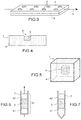
- FIG. 4 represents a longitudinal sectional view of a fourth possible embodiment of the invention, in which the part does not comprise a support device and the extension element is a layer in which a non-through well is made;
- FIG. 5 represents a perspective view of a fifth possible embodiment of the invention, in which the part does not comprise a support device and the extension element is a block in which a closed well is made;
- FIG. 6 represents a sixth possible embodiment of the invention, in which the part comprises an EppendorfTM type tube that acts as a support device;
- FIG. 7 represents a seventh possible embodiment of the invention, in which the part comprises an EppendorfTM type tube with a conical shaped end that acts as a support device;
- FIGS. 8 a and 8 b represent the map of peak electric fields (in absolute value) in a horizontal cut plane passing through the centre of the object under test, for the object under test in a particular extension element ( FIG. 8 a ) and for the object under test alone ( FIG. 8 b ) respectively;
- FIGS. 9 a and 9 b represent the associated profile read on the x axis (direction of the incident electrical field) in the object under test, for the object under test in an extension element ( FIG. 9 a ) and for the object under test alone ( FIG. 9 b ) respectively;
- FIGS. 10 a and 10 b represent the variations with time of component Ex (where Ex is the component parallel to the incident electrical field) at the centre of the object under test in an extension element ( FIG. 10 a ) and for the object under test alone ( FIG. 10 b ), respectively;
- the principle on which this invention is based consists of artificially modifying the geometry of the object to be tested so as to artificially prolong the dimensions of the object to be tested by using an extension material with electrical characteristics similar to those of the object.
- the material with which the extension of the volume of the OUT is made must have a relative permittivity and preferably an electrical conductivity as close as possible to those of the object to be tested, so as to form the globally most uniform possible volume.
- the material from which the extension element(s) is (are) made may be a composite material, a ceramic or a gel, etc.
- the assembly formed by the object to be tested and its 3 d extension 10 then behave like a single object.
- the level of the electric field induced in the object under test depends on the global dimensions of the “object to be tested+extension” assembly, and more particularly its dimensions along the direction of the electric field.
- the distribution of the electric field depends on the global geometry, independently of the geometry of the object to be tested.
- the uniformity and intensity of the field in the object to be tested is significantly improved compared with an “object to be tested alone” configuration.
- the total length of the extension material along the passage direction of the cavity can both compensate for the resulting edge non-uniformity caused, in prior art, by the walls of the container in which the object to be tested is placed and the surrounding vacuum, and also increase the coupling length with the incident electric field.
- the total length of the extension material shall be chosen as a function of the required degree of improvement.
- the extension material is then useful principally for making the induced electric field uniform and the total length of the extension material may be as low as 1 ⁇ 3 of the length of the cavity.
- the extension material in addition to its role of increasing uniformity, also has the effect of increasing the coupling length. Therefore the total length of the extension material must be much longer than in the previous case. For example, in the example illustrated below there is a ratio of more than 10 between the length of the “object under test+extension material” assembly along the passage direction and the length of the cavity.
- the optimal coupling length (the “object under test+extension material” being considered like an antenna in reception) is a fraction of the incident wave length. If this length is too short, coupling will not be improved much; but if this length is too long, there is a risk of stationary waves developing within the “object under test+extension material” assembly. Therefore the one skilled in the art will have to adjust the length of the extension material depending on the required results.
- extension element(s) it is possible to obtain an extension of the volume of the object to be tested along one direction (1D extension) (see the example of the EppendorfTM tube below), along two directions (2D extension) (see the two examples below of a plate and a Petri box) and along three dimensions (3D extension).
- the part may include a support device.
- This support device may be in various forms (Petri box, well plate, microscope slide, EppendorfTM tube, etc.) and must be adapted to the specific features of experiments and the nature of objects under test, that will define the composition of the extension material (ceramic, gel, etc.). Note that the choice of the support device and the extension material must take account of various constraints on the geometry, electrical properties, mechanical and chemical properties (for example such as the resistance to sterilisation, if the support device and the extension element(s) is (are) to be reused).
- the object to be tested is a 12.5 ⁇ L suspension containing Giant Unilammelar cells (GUV) in a solution of 1,2-dioleoyl-sn-glycero-3-phosphocholine (DOPC).
- the relative permittivity of the object is 73.75 and its electrical conductivity is 1.73 S/m at the frequency of 1.5 GHz.
- the extension element(s) is (are) made of agar agar, that has a relative permittivity of 76 and an electrical conductivity of 0.37 S/m at this frequency.
- the part 1 comprises a support device 6 that is a Petri box and the extension element 4 is a layer of agar-agar deposited in the Petri box, in which a well is made that will form the cavity 2 inside which the object to be tested 3 will be located.
- the well is made in the layer at the centre of the Petri box so as to maximise the length of the extension element on each side of the cavity.
- the layer delimits the cavity along the passage direction 5 over the entire lateral cylindrical wall of the cavity (in the plane of the layer).
- the circular wall forming the bottom of the cavity is formed by the support device (the Petri box). Therefore the incident electric field may be directed indifferently in the plane of the layer. The constraint on the direction of the electric field is then eliminated.
- This geometry becomes compatible with the use of an incident electromagnetic wave with circular polarisation or an incident wave with elliptical polarisation, for which the direction of the electric field rotates in a plane parallel to the surface of the bottom of the Petri box.
- the volume of the object to be tested can be reduced to the volume of a disk a few millimetres thick located at the centre of a hollowed out disk formed by a layer made of a material with dielectric characteristics similar to those of the object to be tested.
- the part 1 comprises a support device 6 that is a standard glass microscope slide (24 ⁇ 80 mm), on which a 1 mm (thickness not critical) layer of agar agar is deposited.
- the layer also includes at its centre a cylindrical well that forms the cavity 2 for the object to be tested 3 .
- a glass slide can be added above the agar agar layer to make sure that the well is leak tight and to allow vertical positioning of the part during illumination by a wave with horizontal incidence, or top-down positioning during observations under a microscope.
- FIG. 3 shows a third embodiment of the invention. This embodiment can be used to test several objects to be tested simultaneously.
- the well(s) can be made in all or some of the thickness of the layer of extension material. If the layer made of an extension material is located on a support device, the well(s) can be through wells and can pass through the thickness of the layer.
- FIG. 4 shows a fourth embodiment that is the case for a non-through well made in a thick layer made of extension material. This configuration eliminates the need to use a support device, since the extension volume performs the twofold function of cavity and support.
- a closed cavity can also be made inside a block made of extension material, as shown in FIG. 5 . The result is that the volume of the object is extended in the three dimensions.
- the part 1 includes a hollow support device that is a cylindrical tube such as an EppendorfTM type tube, and the extension element is composed of two plugs 41 , 42 made of agar agar, placed at the ends of the tube, the object to be tested 3 being placed in the tube between these two plugs.
- a conical EppendorfTM type tube is used ( FIG. 7 )
- this solution has the advantage that it avoids the additional non-uniformity added inside the tube by this particular geometry.
- the dimension of the extension material in the direction of incidence of the electric field regulates the amplitude of the electric field induced in the object to be tested.
- a relative permittivity ( ⁇ r ) of 80 for an object to be tested in the form of a 4 mm diameter 1 mm thick disk, a relative permittivity ( ⁇ r ) of 80 , an electrical conductivity ( ⁇ ) of 1.5 S/m at a frequency of 1.5 GHz, and a 24 mm ⁇ 80 mm ⁇ 1 mm virtual extension material (but that could be a low loss ceramic) with a relative permittivity of 60 and zero electrical conductivity at this frequency.
- the ratio between the maximum intensity of the electric field induced at the centre of the object under test and the intensity of the incident electric field varies from 10% (without extension material) to 100% (with extension material).
- the non-uniformity ratio varies from 800% (without extension material) to 14% (with extension material).
- FIGS. 8 a and 8 b , 9 a and 9 b , 10 a and 10 b contain the results obtained using a plane electromagnetic wave with normal incidence, for the configuration with extension material ( FIGS. 8 a , 9 a and 10 a ) and for the configuration without extension material ( FIGS. 8 b , 9 b and 10 b ) respectively.
- gains due to the use of an extension are more than an order of magnitude, both in terms of the intensity of the induced electric field and the uniformity of the electric field in the volume of the object under test, despite significant differences in permittivity and conductivity of the object under test and the extension material.
Landscapes
- Physics & Mathematics (AREA)
- Health & Medical Sciences (AREA)
- Life Sciences & Earth Sciences (AREA)
- Chemical & Material Sciences (AREA)
- General Physics & Mathematics (AREA)
- Engineering & Computer Science (AREA)
- Analytical Chemistry (AREA)
- Pathology (AREA)
- Immunology (AREA)
- General Health & Medical Sciences (AREA)
- Biochemistry (AREA)
- Biomedical Technology (AREA)
- Electromagnetism (AREA)
- Molecular Biology (AREA)
- Medicinal Chemistry (AREA)
- Food Science & Technology (AREA)
- Urology & Nephrology (AREA)
- Optics & Photonics (AREA)
- Hematology (AREA)
- Biophysics (AREA)
- Investigating Or Analyzing Materials By The Use Of Electric Means (AREA)
Applications Claiming Priority (3)
| Application Number | Priority Date | Filing Date | Title |
|---|---|---|---|
| FR1454821A FR3021743B1 (fr) | 2014-05-28 | 2014-05-28 | Procede de preparation d'un objet a tester et procede d'amelioration de l'homogeneite et de l'intensite d'un champ electrique induit dans cet objet illumine par une onde electromagnetique incidente |
| FR1454821 | 2014-05-28 | ||
| PCT/EP2015/061758 WO2015181258A1 (fr) | 2014-05-28 | 2015-05-27 | Procede de preparation d'un objet a tester et procede d'amelioration de l'homogeneite et de l'intensite d'un champ electrique induit dans cet objet illumine par une onde electromagnetique incidente |
Publications (2)
| Publication Number | Publication Date |
|---|---|
| US20170184648A1 US20170184648A1 (en) | 2017-06-29 |
| US10690710B2 true US10690710B2 (en) | 2020-06-23 |
Family
ID=51659746
Family Applications (1)
| Application Number | Title | Priority Date | Filing Date |
|---|---|---|---|
| US15/312,867 Expired - Fee Related US10690710B2 (en) | 2014-05-28 | 2015-05-27 | Method for preparing an object to be tested and method for improving the uniformity and intensity of an electric field induced in said object illuminated by an incident electromagnetic wave |
Country Status (6)
| Country | Link |
|---|---|
| US (1) | US10690710B2 (fr) |
| EP (1) | EP3149498B1 (fr) |
| ES (1) | ES2769817T3 (fr) |
| FR (1) | FR3021743B1 (fr) |
| SI (1) | SI3149498T1 (fr) |
| WO (1) | WO2015181258A1 (fr) |
Families Citing this family (1)
| Publication number | Priority date | Publication date | Assignee | Title |
|---|---|---|---|---|
| FR3164477A1 (fr) | 2024-07-10 | 2026-01-16 | Commissariat A L' Energie Atomique Et Aux Energies Alternatives | Dispositif d’application d'une onde électromagnétique sur un échantillon de matière biologique |
Citations (4)
| Publication number | Priority date | Publication date | Assignee | Title |
|---|---|---|---|---|
| US5748002A (en) * | 1996-01-26 | 1998-05-05 | Phase Dynamics Inc. | RF probe for montoring composition of substances |
| US20010050810A1 (en) | 1997-09-04 | 2001-12-13 | Lorincz Andrew E. | Microscope slide having culture media and method for use |
| US20050215020A1 (en) * | 2001-12-28 | 2005-09-29 | Leif Bergstedt | Component for electromagnetic waves and a method for manufacturing the same |
| US20180076502A1 (en) * | 2015-03-30 | 2018-03-15 | Commissariat A L'energie Atomique Et Aux Energies Alternatives | Device for exposing at least one object to an electromagnetic field having a low input reflection coefficient |
Family Cites Families (1)
| Publication number | Priority date | Publication date | Assignee | Title |
|---|---|---|---|---|
| US5084910A (en) * | 1990-12-17 | 1992-01-28 | Dow Corning Corporation | X-ray diffractometer sample holder |
-
2014
- 2014-05-28 FR FR1454821A patent/FR3021743B1/fr not_active Expired - Fee Related
-
2015
- 2015-05-27 SI SI201531058T patent/SI3149498T1/sl unknown
- 2015-05-27 US US15/312,867 patent/US10690710B2/en not_active Expired - Fee Related
- 2015-05-27 ES ES15725615T patent/ES2769817T3/es active Active
- 2015-05-27 EP EP15725615.7A patent/EP3149498B1/fr active Active
- 2015-05-27 WO PCT/EP2015/061758 patent/WO2015181258A1/fr not_active Ceased
Patent Citations (4)
| Publication number | Priority date | Publication date | Assignee | Title |
|---|---|---|---|---|
| US5748002A (en) * | 1996-01-26 | 1998-05-05 | Phase Dynamics Inc. | RF probe for montoring composition of substances |
| US20010050810A1 (en) | 1997-09-04 | 2001-12-13 | Lorincz Andrew E. | Microscope slide having culture media and method for use |
| US20050215020A1 (en) * | 2001-12-28 | 2005-09-29 | Leif Bergstedt | Component for electromagnetic waves and a method for manufacturing the same |
| US20180076502A1 (en) * | 2015-03-30 | 2018-03-15 | Commissariat A L'energie Atomique Et Aux Energies Alternatives | Device for exposing at least one object to an electromagnetic field having a low input reflection coefficient |
Non-Patent Citations (10)
| Title |
|---|
| Angulo, et al., Improving the SAR Distribution in Petri-Dish Cell Cultures, Journal of Electromagnetic Waves and Applications, vol. 24, XP55164688, 2010, 14 pages. |
| Fontana, et al., "On the Influence of a Glas Slide on the SAR Distribution in Petri Dishes for In Vitro Exposure to 2.45 GHz EM Fields", Antennas and propagation society international symposium (APSURSI), 2010, 4 pages. |
| French Search Report dated Jan. 26, 2015, in French Patent Application No. 1454821, filed May 28, 2014. |
| International Preliminary Report on Patentability dated Jul. 8, 2016, in PCT/EP2015/061758, filed May 27, 2015. |
| International Search Report dated Jun. 25, 2015, in PCT/EP2015/061758, filed May 27, 2015. |
| L. D. ANGULO, S. G. GARCIA, M. F. PANTOJA, C. C. SANCHEZ, R. G. MART�N: "Improving the SAR Distribution in Petri-Dish Cell Cultures", JOURNAL OF ELECTROMAGNETIC WAVES AND APPLICATIONS, VSP, vol. 24, no. 5-6, 1 January 2010 (2010-01-01), pages 815 - 826, XP055164688, ISSN: 09205071, DOI: 10.1163/156939310791036322 |
| Laval, et al. "A New In Vitro Exposure Device for the Mobile Frequency of 900 MHz", Bioelectromagnetics vol. 21, 2000, 9 pages. |
| SCHUDERER J, ET AL.: "IN VITRO EXPOSURE SYSTEMS FOR RF EXPOSURES AT 900 MHZ", IEEE TRANSACTIONS ON MICROWAVE THEORY AND TECHNIQUES, PLENUM, USA, vol. 52, no. 08, PART 02, 1 August 2004 (2004-08-01), USA, pages 2067 - 2075, XP001200626, ISSN: 0018-9480, DOI: 10.1109/TMTT.2004.832010 |
| Schuderer, et al. "In Vitro Exposure Systems for RF Exposures at 900 MHz", IEEE Transactions on Microwave Theory and Techniques, vol. 52, No. 8, XP-001200626, Aug. 2004, 9 pages. |
| U.S. Appl. No. 14/648,977, filed Jun. 2, 2015, US 2015/0299640, Rene Vezinet et al. |
Also Published As
| Publication number | Publication date |
|---|---|
| FR3021743B1 (fr) | 2016-07-29 |
| US20170184648A1 (en) | 2017-06-29 |
| SI3149498T1 (sl) | 2020-03-31 |
| WO2015181258A1 (fr) | 2015-12-03 |
| ES2769817T3 (es) | 2020-06-29 |
| EP3149498A1 (fr) | 2017-04-05 |
| EP3149498B1 (fr) | 2019-10-09 |
| FR3021743A1 (fr) | 2015-12-04 |
Similar Documents
| Publication | Publication Date | Title |
|---|---|---|
| CN107275805B (zh) | 一种基于超材料电磁特性的相控阵天线 | |
| Da Xu et al. | Microstrip patch antennas with multiple parasitic patches and shorting vias for bandwidth enhancement | |
| Elwi | Electromagnetic band gap structures based on ultra wideband microstrip antenna | |
| Chiapperino et al. | Nonlinear dispersive model of electroporation for irregular nucleated cells | |
| Nur et al. | Theoretical analysis of resonant frequency for AMC-based absorber composed of square patch array | |
| US20170184648A1 (en) | Method for preparing an object to be tested and method for improving the uniformity and intensity of an electric field induced in said object illuminated by an incident electromagnetic wave | |
| US10777871B2 (en) | Device for exposing at least one object to an electromagnetic field having a low input reflection coefficient | |
| CN110777073A (zh) | 一种用于细胞实验的宽带电磁辐射装置 | |
| Wang et al. | On the physics of both surface overcharging and charge reversal at heterophase interfaces | |
| Paffi et al. | In vitro exposure: linear and non‐linear thermodynamic events in Petri dishes | |
| Kordzadeh et al. | Permittivity measurement of liquids, powders, and suspensions using a parallel‐plate cell | |
| US9714407B2 (en) | Device for applying an electromagnetic field to a biological sample | |
| Liu et al. | Isolation enhancement of patch antenna array via metamaterial integration | |
| Chiu et al. | Inverse scattering of dielectric cylinders buried in a half space | |
| Bucci et al. | Magnetic nanoparticle enhanced microwave imaging: Towards an experimental feasibility assessment | |
| CN106622067B (zh) | 构建复杂多域非均匀电场的物理系统 | |
| Tayyar et al. | TM scattering by a homogeneously filled slit in a thick impedance screen | |
| Hamzah | Microwave microfluidic resonant sensors and applicators | |
| Nesterenko et al. | Electromagnetic waves scattering by thin impedance vibrators and narrow slots in waveguides | |
| Pillet et al. | High power electromagnetic pulse applicators for evaluation of biological effects induced by electromagnetic radiation waves | |
| Boybay et al. | Double negative metamaterials for subsurface detection | |
| Randa et al. | 3D-FDTD method for analysis of rectangular waveguide loaded with anisotropic dielectric material | |
| Ranga et al. | Width modulated microstrip line patterned surface for isotropic cloak | |
| Li et al. | Probing electric field in an enclosed field mapper for characterizing metamaterials | |
| Skobelev et al. | A new type of the quasi-TEM eigenmodes in a rectangular waveguide with one corrugated hard wall |
Legal Events
| Date | Code | Title | Description |
|---|---|---|---|
| AS | Assignment |
Owner name: COMMISSARIAT A L'ENERGIE ATOMIQUE ET AUX ENERGIES ALTERNATIVES, FRANCE Free format text: ASSIGNMENT OF ASSIGNORS INTEREST;ASSIGNORS:VEZINET, RENE;CATRAIN, ALEXANDRE;CHRETIENNOT, THOMAS;REEL/FRAME:040392/0363 Effective date: 20161107 Owner name: COMMISSARIAT A L'ENERGIE ATOMIQUE ET AUX ENERGIES Free format text: ASSIGNMENT OF ASSIGNORS INTEREST;ASSIGNORS:VEZINET, RENE;CATRAIN, ALEXANDRE;CHRETIENNOT, THOMAS;REEL/FRAME:040392/0363 Effective date: 20161107 |
|
| STPP | Information on status: patent application and granting procedure in general |
Free format text: NON FINAL ACTION MAILED |
|
| STPP | Information on status: patent application and granting procedure in general |
Free format text: RESPONSE TO NON-FINAL OFFICE ACTION ENTERED AND FORWARDED TO EXAMINER |
|
| STPP | Information on status: patent application and granting procedure in general |
Free format text: NOTICE OF ALLOWANCE MAILED -- APPLICATION RECEIVED IN OFFICE OF PUBLICATIONS |
|
| ZAAA | Notice of allowance and fees due |
Free format text: ORIGINAL CODE: NOA |
|
| ZAAB | Notice of allowance mailed |
Free format text: ORIGINAL CODE: MN/=. |
|
| STPP | Information on status: patent application and granting procedure in general |
Free format text: PUBLICATIONS -- ISSUE FEE PAYMENT VERIFIED |
|
| STCF | Information on status: patent grant |
Free format text: PATENTED CASE |
|
| CC | Certificate of correction | ||
| FEPP | Fee payment procedure |
Free format text: MAINTENANCE FEE REMINDER MAILED (ORIGINAL EVENT CODE: REM.); ENTITY STATUS OF PATENT OWNER: LARGE ENTITY |
|
| LAPS | Lapse for failure to pay maintenance fees |
Free format text: PATENT EXPIRED FOR FAILURE TO PAY MAINTENANCE FEES (ORIGINAL EVENT CODE: EXP.); ENTITY STATUS OF PATENT OWNER: LARGE ENTITY |
|
| STCH | Information on status: patent discontinuation |
Free format text: PATENT EXPIRED DUE TO NONPAYMENT OF MAINTENANCE FEES UNDER 37 CFR 1.362 |
|
| FP | Lapsed due to failure to pay maintenance fee |
Effective date: 20240623 |