US10684401B2 - Display device and electronic apparatus - Google Patents
Display device and electronic apparatus Download PDFInfo
- Publication number
- US10684401B2 US10684401B2 US16/080,089 US201716080089A US10684401B2 US 10684401 B2 US10684401 B2 US 10684401B2 US 201716080089 A US201716080089 A US 201716080089A US 10684401 B2 US10684401 B2 US 10684401B2
- Authority
- US
- United States
- Prior art keywords
- light emitting
- display device
- misalignment
- display
- center
- Prior art date
- Legal status (The legal status is an assumption and is not a legal conclusion. Google has not performed a legal analysis and makes no representation as to the accuracy of the status listed.)
- Active, expires
Links
- 238000004020 luminiscence type Methods 0.000 claims abstract description 153
- 239000000758 substrate Substances 0.000 claims abstract description 59
- 238000009826 distribution Methods 0.000 claims description 8
- 230000008859 change Effects 0.000 claims description 5
- 239000010410 layer Substances 0.000 description 91
- 238000000034 method Methods 0.000 description 84
- 239000010408 film Substances 0.000 description 68
- 239000000463 material Substances 0.000 description 48
- 238000012986 modification Methods 0.000 description 37
- 230000004048 modification Effects 0.000 description 37
- 238000010586 diagram Methods 0.000 description 30
- 239000012044 organic layer Substances 0.000 description 23
- VYPSYNLAJGMNEJ-UHFFFAOYSA-N Silicium dioxide Chemical compound O=[Si]=O VYPSYNLAJGMNEJ-UHFFFAOYSA-N 0.000 description 21
- 230000003287 optical effect Effects 0.000 description 21
- 230000007704 transition Effects 0.000 description 19
- 238000005401 electroluminescence Methods 0.000 description 17
- 230000000694 effects Effects 0.000 description 15
- 239000011229 interlayer Substances 0.000 description 15
- 239000003086 colorant Substances 0.000 description 11
- 238000005516 engineering process Methods 0.000 description 11
- 238000007740 vapor deposition Methods 0.000 description 10
- 229910045601 alloy Inorganic materials 0.000 description 9
- 239000000956 alloy Substances 0.000 description 9
- 229910052782 aluminium Inorganic materials 0.000 description 9
- XAGFODPZIPBFFR-UHFFFAOYSA-N aluminium Chemical compound [Al] XAGFODPZIPBFFR-UHFFFAOYSA-N 0.000 description 9
- 229910052681 coesite Inorganic materials 0.000 description 9
- 229910052906 cristobalite Inorganic materials 0.000 description 9
- 238000002156 mixing Methods 0.000 description 9
- 239000000377 silicon dioxide Substances 0.000 description 9
- 229910052682 stishovite Inorganic materials 0.000 description 9
- 229910052905 tridymite Inorganic materials 0.000 description 9
- BQCADISMDOOEFD-UHFFFAOYSA-N Silver Chemical compound [Ag] BQCADISMDOOEFD-UHFFFAOYSA-N 0.000 description 8
- 230000009467 reduction Effects 0.000 description 8
- 239000011347 resin Substances 0.000 description 8
- 229920005989 resin Polymers 0.000 description 8
- 239000004332 silver Substances 0.000 description 8
- 238000005229 chemical vapour deposition Methods 0.000 description 7
- 238000005530 etching Methods 0.000 description 7
- 210000005252 bulbus oculi Anatomy 0.000 description 6
- 230000006872 improvement Effects 0.000 description 6
- 229920000642 polymer Polymers 0.000 description 6
- 229910052709 silver Inorganic materials 0.000 description 6
- 239000011521 glass Substances 0.000 description 5
- 238000002347 injection Methods 0.000 description 5
- 239000007924 injection Substances 0.000 description 5
- 230000000903 blocking effect Effects 0.000 description 4
- 239000010949 copper Substances 0.000 description 4
- 238000002474 experimental method Methods 0.000 description 4
- 239000004973 liquid crystal related substance Substances 0.000 description 4
- 238000000059 patterning Methods 0.000 description 4
- 238000000206 photolithography Methods 0.000 description 4
- 238000007639 printing Methods 0.000 description 4
- 238000007789 sealing Methods 0.000 description 4
- 239000013589 supplement Substances 0.000 description 4
- 229910001316 Ag alloy Inorganic materials 0.000 description 3
- RYGMFSIKBFXOCR-UHFFFAOYSA-N Copper Chemical compound [Cu] RYGMFSIKBFXOCR-UHFFFAOYSA-N 0.000 description 3
- 229910000861 Mg alloy Inorganic materials 0.000 description 3
- KKCBUQHMOMHUOY-UHFFFAOYSA-N Na2O Inorganic materials [O-2].[Na+].[Na+] KKCBUQHMOMHUOY-UHFFFAOYSA-N 0.000 description 3
- PXHVJJICTQNCMI-UHFFFAOYSA-N Nickel Chemical compound [Ni] PXHVJJICTQNCMI-UHFFFAOYSA-N 0.000 description 3
- KDLHZDBZIXYQEI-UHFFFAOYSA-N Palladium Chemical compound [Pd] KDLHZDBZIXYQEI-UHFFFAOYSA-N 0.000 description 3
- 230000015572 biosynthetic process Effects 0.000 description 3
- 239000011575 calcium Substances 0.000 description 3
- 238000006243 chemical reaction Methods 0.000 description 3
- 229910052802 copper Inorganic materials 0.000 description 3
- 238000006073 displacement reaction Methods 0.000 description 3
- 239000010931 gold Substances 0.000 description 3
- 230000005525 hole transport Effects 0.000 description 3
- 229910052751 metal Inorganic materials 0.000 description 3
- 239000002184 metal Substances 0.000 description 3
- 239000000203 mixture Substances 0.000 description 3
- BASFCYQUMIYNBI-UHFFFAOYSA-N platinum Chemical compound [Pt] BASFCYQUMIYNBI-UHFFFAOYSA-N 0.000 description 3
- 229920001721 polyimide Polymers 0.000 description 3
- 239000004065 semiconductor Substances 0.000 description 3
- 229910052814 silicon oxide Inorganic materials 0.000 description 3
- 229910000882 Ca alloy Inorganic materials 0.000 description 2
- OYPRJOBELJOOCE-UHFFFAOYSA-N Calcium Chemical compound [Ca] OYPRJOBELJOOCE-UHFFFAOYSA-N 0.000 description 2
- YCKRFDGAMUMZLT-UHFFFAOYSA-N Fluorine atom Chemical compound [F] YCKRFDGAMUMZLT-UHFFFAOYSA-N 0.000 description 2
- 229910019015 Mg-Ag Inorganic materials 0.000 description 2
- 229910000583 Nd alloy Inorganic materials 0.000 description 2
- 229920001665 Poly-4-vinylphenol Polymers 0.000 description 2
- 239000004372 Polyvinyl alcohol Substances 0.000 description 2
- XUIMIQQOPSSXEZ-UHFFFAOYSA-N Silicon Chemical compound [Si] XUIMIQQOPSSXEZ-UHFFFAOYSA-N 0.000 description 2
- GWEVSGVZZGPLCZ-UHFFFAOYSA-N Titan oxide Chemical compound O=[Ti]=O GWEVSGVZZGPLCZ-UHFFFAOYSA-N 0.000 description 2
- 239000011651 chromium Substances 0.000 description 2
- 239000004020 conductor Substances 0.000 description 2
- 238000012937 correction Methods 0.000 description 2
- 239000011737 fluorine Substances 0.000 description 2
- 229910052731 fluorine Inorganic materials 0.000 description 2
- 229910052839 forsterite Inorganic materials 0.000 description 2
- PCHJSUWPFVWCPO-UHFFFAOYSA-N gold Chemical compound [Au] PCHJSUWPFVWCPO-UHFFFAOYSA-N 0.000 description 2
- 229910052737 gold Inorganic materials 0.000 description 2
- 229910052738 indium Inorganic materials 0.000 description 2
- APFVFJFRJDLVQX-UHFFFAOYSA-N indium atom Chemical compound [In] APFVFJFRJDLVQX-UHFFFAOYSA-N 0.000 description 2
- 238000007641 inkjet printing Methods 0.000 description 2
- 238000004519 manufacturing process Methods 0.000 description 2
- 239000011159 matrix material Substances 0.000 description 2
- 238000005259 measurement Methods 0.000 description 2
- 230000007935 neutral effect Effects 0.000 description 2
- ZKATWMILCYLAPD-UHFFFAOYSA-N niobium pentoxide Chemical compound O=[Nb](=O)O[Nb](=O)=O ZKATWMILCYLAPD-UHFFFAOYSA-N 0.000 description 2
- 230000001151 other effect Effects 0.000 description 2
- 238000005240 physical vapour deposition Methods 0.000 description 2
- 229920003229 poly(methyl methacrylate) Polymers 0.000 description 2
- 229920000139 polyethylene terephthalate Polymers 0.000 description 2
- 239000005020 polyethylene terephthalate Substances 0.000 description 2
- 239000009719 polyimide resin Substances 0.000 description 2
- 239000004926 polymethyl methacrylate Substances 0.000 description 2
- 229920002451 polyvinyl alcohol Polymers 0.000 description 2
- 238000012545 processing Methods 0.000 description 2
- 230000000644 propagated effect Effects 0.000 description 2
- 239000010453 quartz Substances 0.000 description 2
- 238000007650 screen-printing Methods 0.000 description 2
- 229910052710 silicon Inorganic materials 0.000 description 2
- 239000010703 silicon Substances 0.000 description 2
- 239000011734 sodium Substances 0.000 description 2
- 238000004544 sputter deposition Methods 0.000 description 2
- 239000010409 thin film Substances 0.000 description 2
- 238000012546 transfer Methods 0.000 description 2
- 239000004925 Acrylic resin Substances 0.000 description 1
- 229920000178 Acrylic resin Polymers 0.000 description 1
- 229910000838 Al alloy Inorganic materials 0.000 description 1
- 229910001148 Al-Li alloy Inorganic materials 0.000 description 1
- 229910001020 Au alloy Inorganic materials 0.000 description 1
- 229910011255 B2O3 Inorganic materials 0.000 description 1
- WKBOTKDWSSQWDR-UHFFFAOYSA-N Bromine atom Chemical compound [Br] WKBOTKDWSSQWDR-UHFFFAOYSA-N 0.000 description 1
- VYZAMTAEIAYCRO-UHFFFAOYSA-N Chromium Chemical compound [Cr] VYZAMTAEIAYCRO-UHFFFAOYSA-N 0.000 description 1
- 229910000881 Cu alloy Inorganic materials 0.000 description 1
- DGAQECJNVWCQMB-PUAWFVPOSA-M Ilexoside XXIX Chemical compound C[C@@H]1CC[C@@]2(CC[C@@]3(C(=CC[C@H]4[C@]3(CC[C@@H]5[C@@]4(CC[C@@H](C5(C)C)OS(=O)(=O)[O-])C)C)[C@@H]2[C@]1(C)O)C)C(=O)O[C@H]6[C@@H]([C@H]([C@@H]([C@H](O6)CO)O)O)O.[Na+] DGAQECJNVWCQMB-PUAWFVPOSA-M 0.000 description 1
- XEEYBQQBJWHFJM-UHFFFAOYSA-N Iron Chemical compound [Fe] XEEYBQQBJWHFJM-UHFFFAOYSA-N 0.000 description 1
- WHXSMMKQMYFTQS-UHFFFAOYSA-N Lithium Chemical compound [Li] WHXSMMKQMYFTQS-UHFFFAOYSA-N 0.000 description 1
- FYYHWMGAXLPEAU-UHFFFAOYSA-N Magnesium Chemical compound [Mg] FYYHWMGAXLPEAU-UHFFFAOYSA-N 0.000 description 1
- 229910052779 Neodymium Inorganic materials 0.000 description 1
- 229910002668 Pd-Cu Inorganic materials 0.000 description 1
- 229920012266 Poly(ether sulfone) PES Polymers 0.000 description 1
- 239000004642 Polyimide Substances 0.000 description 1
- NINIDFKCEFEMDL-UHFFFAOYSA-N Sulfur Chemical compound [S] NINIDFKCEFEMDL-UHFFFAOYSA-N 0.000 description 1
- ATJFFYVFTNAWJD-UHFFFAOYSA-N Tin Chemical compound [Sn] ATJFFYVFTNAWJD-UHFFFAOYSA-N 0.000 description 1
- RTAQQCXQSZGOHL-UHFFFAOYSA-N Titanium Chemical compound [Ti] RTAQQCXQSZGOHL-UHFFFAOYSA-N 0.000 description 1
- HCHKCACWOHOZIP-UHFFFAOYSA-N Zinc Chemical compound [Zn] HCHKCACWOHOZIP-UHFFFAOYSA-N 0.000 description 1
- QCWXUUIWCKQGHC-UHFFFAOYSA-N Zirconium Chemical compound [Zr] QCWXUUIWCKQGHC-UHFFFAOYSA-N 0.000 description 1
- NIXOWILDQLNWCW-UHFFFAOYSA-N acrylic acid group Chemical group C(C=C)(=O)O NIXOWILDQLNWCW-UHFFFAOYSA-N 0.000 description 1
- 229910052783 alkali metal Inorganic materials 0.000 description 1
- 150000001340 alkali metals Chemical class 0.000 description 1
- 229910052784 alkaline earth metal Inorganic materials 0.000 description 1
- 150000001342 alkaline earth metals Chemical class 0.000 description 1
- 230000004075 alteration Effects 0.000 description 1
- 230000005540 biological transmission Effects 0.000 description 1
- 239000005380 borophosphosilicate glass Substances 0.000 description 1
- 239000005388 borosilicate glass Substances 0.000 description 1
- GDTBXPJZTBHREO-UHFFFAOYSA-N bromine Substances BrBr GDTBXPJZTBHREO-UHFFFAOYSA-N 0.000 description 1
- 229910052794 bromium Inorganic materials 0.000 description 1
- 229910052791 calcium Inorganic materials 0.000 description 1
- ODINCKMPIJJUCX-UHFFFAOYSA-N calcium oxide Inorganic materials [Ca]=O ODINCKMPIJJUCX-UHFFFAOYSA-N 0.000 description 1
- 238000004364 calculation method Methods 0.000 description 1
- 229910052804 chromium Inorganic materials 0.000 description 1
- 229910017052 cobalt Inorganic materials 0.000 description 1
- 239000010941 cobalt Substances 0.000 description 1
- GUTLYIVDDKVIGB-UHFFFAOYSA-N cobalt atom Chemical compound [Co] GUTLYIVDDKVIGB-UHFFFAOYSA-N 0.000 description 1
- 238000000151 deposition Methods 0.000 description 1
- 238000013461 design Methods 0.000 description 1
- 238000011161 development Methods 0.000 description 1
- 210000005069 ears Anatomy 0.000 description 1
- 238000007772 electroless plating Methods 0.000 description 1
- 238000010894 electron beam technology Methods 0.000 description 1
- 238000009713 electroplating Methods 0.000 description 1
- 239000003822 epoxy resin Substances 0.000 description 1
- 238000000605 extraction Methods 0.000 description 1
- 239000003353 gold alloy Substances 0.000 description 1
- 238000004050 hot filament vapor deposition Methods 0.000 description 1
- 238000011835 investigation Methods 0.000 description 1
- 238000007733 ion plating Methods 0.000 description 1
- 238000000608 laser ablation Methods 0.000 description 1
- 239000005355 lead glass Substances 0.000 description 1
- YEXPOXQUZXUXJW-UHFFFAOYSA-N lead(II) oxide Inorganic materials [Pb]=O YEXPOXQUZXUXJW-UHFFFAOYSA-N 0.000 description 1
- 229910052744 lithium Inorganic materials 0.000 description 1
- 239000011777 magnesium Substances 0.000 description 1
- 229910052749 magnesium Inorganic materials 0.000 description 1
- HCWCAKKEBCNQJP-UHFFFAOYSA-N magnesium orthosilicate Chemical compound [Mg+2].[Mg+2].[O-][Si]([O-])([O-])[O-] HCWCAKKEBCNQJP-UHFFFAOYSA-N 0.000 description 1
- 238000002844 melting Methods 0.000 description 1
- 230000008018 melting Effects 0.000 description 1
- 238000002488 metal-organic chemical vapour deposition Methods 0.000 description 1
- 239000002365 multiple layer Substances 0.000 description 1
- QEFYFXOXNSNQGX-UHFFFAOYSA-N neodymium atom Chemical compound [Nd] QEFYFXOXNSNQGX-UHFFFAOYSA-N 0.000 description 1
- 229910052759 nickel Inorganic materials 0.000 description 1
- 229920003986 novolac Polymers 0.000 description 1
- 238000001579 optical reflectometry Methods 0.000 description 1
- 238000013041 optical simulation Methods 0.000 description 1
- 239000011368 organic material Substances 0.000 description 1
- 229920000620 organic polymer Polymers 0.000 description 1
- 229910052763 palladium Inorganic materials 0.000 description 1
- 238000005192 partition Methods 0.000 description 1
- 239000005360 phosphosilicate glass Substances 0.000 description 1
- 238000007747 plating Methods 0.000 description 1
- 229910052697 platinum Inorganic materials 0.000 description 1
- 238000005498 polishing Methods 0.000 description 1
- 229920002577 polybenzoxazole Polymers 0.000 description 1
- 229920000515 polycarbonate Polymers 0.000 description 1
- 239000004417 polycarbonate Substances 0.000 description 1
- 229920000647 polyepoxide Polymers 0.000 description 1
- -1 polyethylene terephthalate Polymers 0.000 description 1
- 229920001296 polysiloxane Polymers 0.000 description 1
- 238000002310 reflectometry Methods 0.000 description 1
- 229920002050 silicone resin Polymers 0.000 description 1
- 238000004088 simulation Methods 0.000 description 1
- 239000002356 single layer Substances 0.000 description 1
- 238000005549 size reduction Methods 0.000 description 1
- 239000005361 soda-lime glass Substances 0.000 description 1
- 229910052708 sodium Inorganic materials 0.000 description 1
- 238000003980 solgel method Methods 0.000 description 1
- 239000000243 solution Substances 0.000 description 1
- 229910052712 strontium Inorganic materials 0.000 description 1
- CIOAGBVUUVVLOB-UHFFFAOYSA-N strontium atom Chemical compound [Sr] CIOAGBVUUVVLOB-UHFFFAOYSA-N 0.000 description 1
- 239000000126 substance Substances 0.000 description 1
- 239000011593 sulfur Substances 0.000 description 1
- 229910052717 sulfur Inorganic materials 0.000 description 1
- 229910052715 tantalum Inorganic materials 0.000 description 1
- GUVRBAGPIYLISA-UHFFFAOYSA-N tantalum atom Chemical compound [Ta] GUVRBAGPIYLISA-UHFFFAOYSA-N 0.000 description 1
- 239000010936 titanium Substances 0.000 description 1
- 229910052719 titanium Inorganic materials 0.000 description 1
- 238000002834 transmittance Methods 0.000 description 1
- WFKWXMTUELFFGS-UHFFFAOYSA-N tungsten Chemical compound [W] WFKWXMTUELFFGS-UHFFFAOYSA-N 0.000 description 1
- 229910052721 tungsten Inorganic materials 0.000 description 1
- 239000010937 tungsten Substances 0.000 description 1
- 229910052725 zinc Inorganic materials 0.000 description 1
- 239000011701 zinc Substances 0.000 description 1
- 229910052726 zirconium Inorganic materials 0.000 description 1
Images


Classifications
-
- H—ELECTRICITY
- H05—ELECTRIC TECHNIQUES NOT OTHERWISE PROVIDED FOR
- H05B—ELECTRIC HEATING; ELECTRIC LIGHT SOURCES NOT OTHERWISE PROVIDED FOR; CIRCUIT ARRANGEMENTS FOR ELECTRIC LIGHT SOURCES, IN GENERAL
- H05B33/00—Electroluminescent light sources
- H05B33/02—Details
-
- G—PHYSICS
- G02—OPTICS
- G02B—OPTICAL ELEMENTS, SYSTEMS OR APPARATUS
- G02B5/00—Optical elements other than lenses
- G02B5/20—Filters
-
- G—PHYSICS
- G02—OPTICS
- G02B—OPTICAL ELEMENTS, SYSTEMS OR APPARATUS
- G02B5/00—Optical elements other than lenses
- G02B5/20—Filters
- G02B5/201—Filters in the form of arrays
-
- G—PHYSICS
- G09—EDUCATION; CRYPTOGRAPHY; DISPLAY; ADVERTISING; SEALS
- G09F—DISPLAYING; ADVERTISING; SIGNS; LABELS OR NAME-PLATES; SEALS
- G09F9/00—Indicating arrangements for variable information in which the information is built-up on a support by selection or combination of individual elements
- G09F9/30—Indicating arrangements for variable information in which the information is built-up on a support by selection or combination of individual elements in which the desired character or characters are formed by combining individual elements
- G09F9/33—Indicating arrangements for variable information in which the information is built-up on a support by selection or combination of individual elements in which the desired character or characters are formed by combining individual elements being semiconductor devices, e.g. diodes
-
- H01L27/32—
-
- H01L27/322—
-
- H01L51/50—
-
- H—ELECTRICITY
- H05—ELECTRIC TECHNIQUES NOT OTHERWISE PROVIDED FOR
- H05B—ELECTRIC HEATING; ELECTRIC LIGHT SOURCES NOT OTHERWISE PROVIDED FOR; CIRCUIT ARRANGEMENTS FOR ELECTRIC LIGHT SOURCES, IN GENERAL
- H05B33/00—Electroluminescent light sources
- H05B33/12—Light sources with substantially two-dimensional radiating surfaces
- H05B33/22—Light sources with substantially two-dimensional radiating surfaces characterised by the chemical or physical composition or the arrangement of auxiliary dielectric or reflective layers
-
- H—ELECTRICITY
- H10—SEMICONDUCTOR DEVICES; ELECTRIC SOLID-STATE DEVICES NOT OTHERWISE PROVIDED FOR
- H10K—ORGANIC ELECTRIC SOLID-STATE DEVICES
- H10K50/00—Organic light-emitting devices
-
- H—ELECTRICITY
- H10—SEMICONDUCTOR DEVICES; ELECTRIC SOLID-STATE DEVICES NOT OTHERWISE PROVIDED FOR
- H10K—ORGANIC ELECTRIC SOLID-STATE DEVICES
- H10K59/00—Integrated devices, or assemblies of multiple devices, comprising at least one organic light-emitting element covered by group H10K50/00
-
- H—ELECTRICITY
- H10—SEMICONDUCTOR DEVICES; ELECTRIC SOLID-STATE DEVICES NOT OTHERWISE PROVIDED FOR
- H10K—ORGANIC ELECTRIC SOLID-STATE DEVICES
- H10K59/00—Integrated devices, or assemblies of multiple devices, comprising at least one organic light-emitting element covered by group H10K50/00
- H10K59/30—Devices specially adapted for multicolour light emission
- H10K59/38—Devices specially adapted for multicolour light emission comprising colour filters or colour changing media [CCM]
-
- H—ELECTRICITY
- H10—SEMICONDUCTOR DEVICES; ELECTRIC SOLID-STATE DEVICES NOT OTHERWISE PROVIDED FOR
- H10K—ORGANIC ELECTRIC SOLID-STATE DEVICES
- H10K59/00—Integrated devices, or assemblies of multiple devices, comprising at least one organic light-emitting element covered by group H10K50/00
- H10K59/80—Constructional details
- H10K59/875—Arrangements for extracting light from the devices
- H10K59/878—Arrangements for extracting light from the devices comprising reflective means
-
- H—ELECTRICITY
- H10—SEMICONDUCTOR DEVICES; ELECTRIC SOLID-STATE DEVICES NOT OTHERWISE PROVIDED FOR
- H10K—ORGANIC ELECTRIC SOLID-STATE DEVICES
- H10K59/00—Integrated devices, or assemblies of multiple devices, comprising at least one organic light-emitting element covered by group H10K50/00
- H10K59/80—Constructional details
- H10K59/875—Arrangements for extracting light from the devices
- H10K59/879—Arrangements for extracting light from the devices comprising refractive means, e.g. lenses
Definitions
- the present disclosure relates to a display device and an electronic apparatus.
- Patent Literature 1 discloses a display device that expresses white or a neutral color by color mixing of self-luminous elements of a plurality of simple colors (red, green, and blue) and in which the distance from an end of a luminescence region to an end of an opening of a light blocking layer that is provided on the luminescence region is different between a red luminescence region, a green luminescence region, and a blue luminescence region.
- the rate of luminance reduction by the light blocking of the light blocking layer can be varied between colors by appropriately setting the areas of the openings of the light blocking layers, and thus the differences in viewing angle characteristics between colors can be reduced. Therefore, the chromaticity change of white or a neutral color due to viewing angles can be suppressed.
- Patent Literature 1 JP 2011-40352A
- a display device having a display surface with a relatively small area such as a head-mounted display (HMD) or an electronic viewfinder (EVF) of a digital camera
- HMD head-mounted display
- EVF electronic viewfinder
- a light beam from the display surface of the display device is caused to form an image on an eyeball of a user via an optical system of a lens, a mirror, a diffraction grating, etc.; the optical system tends to be downsized from demand for further reduction in the weight and size of the electronic apparatus.
- the optical system If the optical system is downsized, it becomes necessary that a light beam be caused to form an image on an eyeball of a user appropriately by means of an optical system of a simpler configuration, and hence it is difficult to supplement the viewing angle characteristics of the display device by modifying the configuration of the optical system; the viewing angle characteristics of the display device directly lead to the quality of display that is visually identified by the user. Therefore, depending on the use, the display device is required to achieve even more improvement in viewing angle characteristics.
- the present disclosure presents a new and improved display device that can improve viewing angle characteristics more and an electronic apparatus on which the display device is mounted.
- a display device including: a plurality of light emitting sections formed on a substrate; and a color filter provided on the light emitting section to correspond to each of the plurality of light emitting sections.
- the light emitting sections and the color filters are arranged such that, in at least a partial region in a display surface, a relative misalignment between a center of a luminescence surface of the light emitting section and a center of the color filter corresponding to the light emitting section is created in a plane perpendicular to a stacking direction.
- an electronic apparatus including: a display device configured to perform display on a basis of an image signal.
- the display device includes a plurality of light emitting sections formed on a substrate, and a color filter provided on the light emitting section to correspond to each of the plurality of light emitting sections, and the light emitting sections and the color filters are arranged such that, in at least a partial region in a display surface, a relative misalignment between a center of a luminescence surface of the light emitting section and a center of the color filter corresponding to the light emitting section is created in a plane perpendicular to a stacking direction.
- the light emitting sections and the color filters are arranged such that, in at least a partial region in the display surface of the display device, a relative misalignment between the center of the luminescence surface of a light emitting section (for example, in an organic EL display, a light emitting element) and the center of the color filter corresponding to the light emitting section is created in a plane perpendicular to the stacking direction. Therefore, for a pixel including the light emitting section and the color filter, wider viewing angle characteristics can be obtained in the direction of misalignment of the color filter to the luminescence surface of the light emitting section.
- a relative misalignment between the center of the luminescence surface of a light emitting section for example, in an organic EL display, a light emitting element
- the center of the color filter corresponding to the light emitting section is created in a plane perpendicular to the stacking direction. Therefore, for a pixel including the light emitting section and the color filter, wider viewing angle characteristics can be obtained in the direction
- viewing angle characteristics can be improved more.
- the effects described above are not necessarily limitative. With or in the place of the above effects, there may be achieved any one of the effects described in this specification or other effects that may be grasped from this specification.
- FIG. 1 is a diagram simulatively showing a locus of a light beam from a small-sized display device in an electronic apparatus to an eyeball of a user in a case where an optical system is downsized.
- FIG. 2 is a cross-sectional view showing a configuration example of a display device according to the present embodiment.
- FIG. 3 is a diagram for describing an effect exhibited by creating a relative misalignment between a light emitting element and a CF in a display device according to the present embodiment.
- FIG. 4 is a diagram simply and schematically showing a configuration of a common display device.
- FIG. 5 is a diagram for describing distributions of amounts of misalignment L and misalignment directions of CFs in a display surface of a display device.
- FIG. 6 is a diagram for describing a transition region in which the amount of misalignment L and/or the misalignment direction of the CF changes.
- FIG. 7 is a diagram for describing a transition region in which the amount of misalignment L and/or the misalignment direction of the CF changes.
- FIG. 8 is a diagram for describing a method for setting the amount of misalignment L of the CF.
- FIG. 9 is a diagram for describing a method for setting the amount of misalignment L of the CF.
- FIG. 10 is a diagram for describing a method for setting the amount of misalignment L of the CF.
- FIG. 11 is a diagram for describing a method for setting the amount of misalignment L of the CF.
- FIG. 12 is a diagram for describing another method for creating a relative misalignment between a light emitting element and a CF.
- FIG. 13 is a diagram showing a configuration example of a display device according to a modification example in which a reflector is not provided.
- FIG. 14 is a diagram for describing a method for setting the amount of misalignment L of the CF taking into account also a case where emission light from a luminescence section is incident on a side surface of the CF.
- FIG. 15 is a diagram showing an external appearance of a smartphone that is an example of an electronic apparatus in which the display devices according to the present embodiment and the modification examples can be used.
- FIG. 16 is a diagram showing an external appearance of a digital camera that is another example of an electronic apparatus in which the display devices according to the present embodiment and the modification examples can be used.
- FIG. 17 is a diagram showing an external appearance of a digital camera that is another example of an electronic apparatus in which the display devices according to the present embodiment and the modification examples can be used.
- FIG. 18 is a diagram showing an external appearance of an HMD that is another example of an electronic apparatus in which the display devices according to the present embodiment and the modification examples can be used.
- a small-sized display device may be mounted on an electronic apparatus in the use of an HMD, an EVF of a digital camera, etc.
- a light beam from a display surface of the display device is caused to form an image on an eyeball of a user via an optical system of a lens, a mirror, a diffraction grating, etc.
- the mounted optical system is required to achieve even more downsizing.
- FIG. 1 is a diagram simulatively showing the locus of a light beam from a small-sized display device in an electronic apparatus to an eyeball of a user in a case where an optical system is downsized.
- an optical system As shown in FIG. 1 , to achieve reduction in the weight and size of the electronic apparatus, it is necessary to downsize an optical system 105 and make narrower the distance between the optical system 105 and a display device 1 . Further, since the optical system 105 cannot be made a complicated configuration, it is difficult to supplement the viewing angle characteristics of the display device 1 by modifying the configuration of the optical system 105 .
- a light beam with a wider angle that is, a light beam with a wider viewing angle
- a light beam with a wider viewing angle among the light beams emitted from a display surface 101 of the display device 1 is guided to an eyeball 103 of a user while keeping almost the same characteristics as those when the light beam is emitted from the display surface 101 of the display device 1 .
- a display device of a system in which a pixel is formed by providing a color filter (CF) on a white light emitting element and color display is performed by performing color conversion based on the CF on a pixel basis is commonly known. If it is attempted to achieve a wide viewing angle in a display device of such a system, the occurrence of what is called color mixing in which light from one light emitting element is incident on the CF of an adjacent pixel and light emission of a desired color is not obtained is a problem.
- CF color filter
- the display device is an organic EL display
- the present disclosure is not limited to this example, and the display device that is an object of the present disclosure may be various display devices as long as they are display devices that can achieve color display using CFs, such as a liquid crystal display, a plasma display, and an electronic paper device.
- FIG. 2 is a cross-sectional view showing a configuration example of a display device according to the present embodiment.
- FIG. 2 shows a schematic partial cross-sectional view of a display device according to the present embodiment.
- a display device 1 includes, on a first substrate 11 , a plurality of light emitting elements 10 each of which includes an OLED and emits white light, and a CF layer 33 that is provided on the light emitting elements 10 and in which CFs of some colors are formed to correspond to the light emitting elements 10 . Further, a second substrate 34 containing a material transparent to the light from the light emitting element 10 is placed on the CF layer 33 . Further, on the first substrate 11 , thin film transistors (TFTs) 15 for driving the light emitting elements 10 are provided to correspond to the light emitting elements 10 .
- TFTs thin film transistors
- An arbitrary light emitting element 10 is selectively driven by the TFT 15 , then light from the driven light emitting element 10 passes through the corresponding CF, and the color of the light is converted appropriately and the converted light is emitted from the upper side via the second substrate 34 ; thereby, desired images, characters, etc. are displayed.
- the stacking direction of the layers in the display device 1 is referred to also as an up and down direction.
- the side on which the first substrate 11 is placed is defined as a down side
- the side on which the second substrate 34 is placed is defined as an up side.
- a plane perpendicular to the up and down direction is referred to also as a horizontal plane.
- the display device 1 shown in FIG. 2 is a top emission display device capable of color display that is driven by an active matrix system.
- the present embodiment is not limited to this example, and the display device according to the present embodiment may be a display device that is driven by another system such as a passive matrix system, or may be a bottom emission display device that emits light via the first substrate 11 .
- the display device 1 may be mounted on various electronic apparatuses having a display function.
- the display device 1 may be used as, for example, a monitor device that is incorporated in a television device, an electronic book, a smartphone, a personal digital assistant (PDA), a notebook personal computer (PC), a video camera, a game apparatus, or the like.
- the display device 1 may be used for an EVF of a digital camera, an HMD, or the like.
- the display device 1 has excellent wide viewing angle characteristics even if a complicated optical system is not provided; thus, the display device 1 can be suitably used for, among the above electronic apparatuses, an electronic apparatus that is used by being carried by a user, which is required to achieve weight and size reduction more (among the examples described above, a smartphone, a PDA, a digital camera, an HMD, or the like).
- the first substrate 11 includes a silicon substrate.
- the second substrate 34 contains quartz glass.
- each of the first substrate 11 and the second substrate 34 may include a high strain point glass substrate, a soda-lime glass (a mixture of Na 2 O, CaO, and SiO 2 ) substrate, a borosilicate glass (a mixture of Na 2 O, B 2 O 3 , and SiO 2 ) substrate, a forsterite (Mg 2 SiO 4 ) substrate, a lead glass (a mixture of Na 2 O, PbO, and SiO 2 ) substrate, various glass substrates in which an insulating film is formed on a surface, a quartz substrate, a quartz substrate in which an insulating film is formed on a surface, a silicon substrate in which an insulating film is formed on a surface, or an organic polymer substrate (for example, polymethyl methacrylate (PMMA), PMMA
- the materials contained in the first substrate 11 and the second substrate 34 may be the same, or may be different. However, since the display device 1 is of the top emission type as described above, the second substrate 34 preferably contains a material with a high transmittance that can transmit the light from the light emitting element 10 favorably.
- the light emitting element 10 includes a first electrode 21 , an organic layer 23 provided on the first electrode 21 , and a second electrode 22 formed on the organic layer 23 . More specifically, a second member 52 in which openings 25 are provided so as to expose at least parts of the first electrode 21 is stacked on the first electrode 21 , and the organic layer 23 is provided on portions of the first electrode 21 that are exposed at the bottoms of the openings 25 . That is, the light emitting element 10 has a configuration in which the first electrode 21 , the organic layer 23 , and the second electrode 22 are stacked in this order in the opening 25 of the second member 52 . This stacked structure functions as a luminescence section 24 of each pixel. That is, a portion of the light emitting element 10 falling under the opening 25 of the second member 52 serves as a luminescence surface. Further, the second member 52 functions as a pixel defining film that is provided between pixels and partitions the area of the pixel.
- the organic layer 23 includes a luminescence layer containing an organic luminescent material, and can emit white light.
- the specific configuration of the organic layer 23 is not limited, and may be various publicly known configurations.
- the organic layer 23 may have a stacked structure of a hole transport layer, a luminescence layer, and an electronic transport layer, a stacked structure of a hole transport layer and a luminescence layer that serves also as an electronic transport layer, a stacked structure of a hole injection layer, a hole transport layer, a luminescence layer, an electronic transport layer, and an electron injection layer, or the like.
- the organic layer 23 may have a tandem structure of two stages in which a first tandem unit, a connection layer, and a second tandem unit are stacked. Alternatively, the organic layer 23 may have a tandem structure of three or more stages in which three or more tandem units are stacked. In a case where the organic layer 23 includes a plurality of tandem units, an organic layer 23 that emits white light as a whole can be obtained by assigning red, green, and blue to the luminescent colors of the luminescence layers of the tandem units.
- the organic layer 23 is formed by depositing an organic material by vacuum vapor deposition.
- the present embodiment is not limited to this example, and the organic layer 23 may be formed by various publicly known methods.
- the method for forming the organic layer 23 physical vapor deposition methods (PVD methods) such as the vacuum vapor deposition method, printing methods such as the screen printing method and the inkjet printing method, a laser transfer method in which a stacked structure of a laser absorbing layer and an organic layer formed on a substrate for transfer is irradiated with laser light to separate the organic layer on the laser absorbing layer and the organic layer is transferred, various application methods, etc. may be used.
- PVD methods physical vapor deposition methods
- printing methods such as the screen printing method and the inkjet printing method
- a laser transfer method in which a stacked structure of a laser absorbing layer and an organic layer formed on a substrate for transfer is irradiated with laser light to separate the organic layer on the laser absorbing layer and the organic layer is transferred, various application methods, etc.
- the first electrode 21 functions as an anode. Since the display device 1 is of the top emission type as described above, the first electrode 21 contains a material capable of reflecting the light from the organic layer 23 . In the illustrated configuration example, the first electrode 21 contains an alloy of aluminum and neodymium (Al—Nd alloy). Further, the film thickness of the first electrode 21 is approximately 0.1 ⁇ m to 1 ⁇ m, for example. However, the present embodiment is not limited to this example, and the first electrode 21 may contain various publicly known materials used as the material of an electrode on the light reflection side that functions as an anode in a common organic EL display. Further, the film thickness of the first electrode 21 is not limited to the above example either, and the first electrode 21 may be formed in film thickness ranges commonly employed in organic EL displays, as appropriate.
- the first electrode 21 may contain a metal with a high work function, such as platinum (Pt), gold (Au), silver (Ag), chromium (Cr), tungsten (W), nickel (Ni), copper (Cu), iron (Fe), cobalt (Co), or tantalum (Ta), or an alloy with a high work function (for example, a Ag—Pd—Cu alloy containing silver as a main component and containing 0.3 mass % to 1 mass % of palladium (Pd) and 0.3 mass % to 1 mass % of copper, an Al—Nd alloy, or the like).
- a metal with a high work function such as platinum (Pt), gold (Au), silver (Ag), chromium (Cr), tungsten (W), nickel (Ni), copper (Cu), iron (Fe), cobalt (Co), or tantalum (Ta), or an alloy with a high work function (for example, a Ag—Pd—Cu alloy containing silver as a main component and containing
- the first electrode 21 may contain an electrically conductive material having a small work function value and a high light reflectance, such as aluminum or an alloy containing aluminum. In this case, it is preferable to improve hole injection properties by providing an appropriate hole injection layer on the first electrode 21 , or the like.
- the first electrode 21 may have a structure in which a transparent electrically conductive material excellent in hole injection characteristics, such as an oxide of indium and tin (ITO) or an oxide of indium and zinc (IZO), is stacked on a reflective film with high light reflectivity such as a dielectric multiple-layer film or aluminum.
- ITO oxide of indium and tin
- IZO oxide of indium and zinc
- the second electrode 22 functions as a cathode. Since the display device 1 is of the top emission type as described above, the second electrode 22 contains a material capable of transmitting the light from the organic layer 23 . In the illustrated configuration example, the second electrode 22 contains an alloy of magnesium and silver (Mg—Ag alloy). Further, the film thickness of the second electrode 22 is approximately 10 nm, for example. However, the present embodiment is not limited to this example, and the second electrode 22 may contain various publicly known materials used as the material of an electrode on the light transmission side that functions as a cathode in a common organic EL display. Further, the film thickness of the second electrode 22 is not limited to the above example either, and the second electrode 22 may be formed in film thickness ranges commonly employed in organic EL displays, as appropriate.
- the second electrode 22 may contain aluminum, silver, magnesium, calcium (Ca), sodium (Na), strontium (Sr), an alloy of an alkali metal and silver, an alloy of an alkaline earth metal and silver (for example, an alloy of magnesium and silver (Mg—Ag alloy)), an alloy of magnesium and calcium (Mg—Ca alloy), an alloy of aluminum and lithium (Al—Li alloy), or the like.
- the film thickness of the second electrode 22 is approximately 4 nm to 50 nm, for example.
- the second electrode 22 may have a structure in which a layer of any of the materials described above and a transparent electrode containing, for example, ITO or IZO (with a thickness of, for example, approximately 30 nm to 1 ⁇ m) are stacked from the organic layer 23 side.
- a transparent electrode containing, for example, ITO or IZO with a thickness of, for example, approximately 30 nm to 1 ⁇ m
- the thickness of the layer of any of the materials described above may be as thin as approximately 1 nm to 4 nm, for example.
- the second electrode 22 may include only a transparent electrode.
- the second electrode 22 may be provided with a bus electrode (auxiliary electrode) containing a low resistance material, such as aluminum, an aluminum alloy, silver, a silver alloy, copper, a copper alloy, gold, or a gold alloy, to reduce the resistance of the second electrode 22 as a whole.
- a bus electrode auxiliary electrode
- a low resistance material such as aluminum, an aluminum alloy, silver, a silver alloy, copper, a copper alloy, gold, or a gold alloy
- each of the first electrode 21 and the second electrode 22 is formed by forming a material as a film with a prescribed thickness by the vacuum vapor deposition method and then patterning the film by the etching method.
- the present embodiment is not limited to this example, and the first electrode 21 and the second electrode 22 may be formed by various publicly known methods.
- Examples of the method for forming the first electrode 21 and the second electrode 22 include vapor deposition methods including the electron beam vapor deposition method, the hot filament vapor deposition method, and the vacuum vapor deposition method, the sputtering method, the chemical vapor deposition method (CVD method), the metal organic chemical vapor deposition method (MOCVD method), a combination of the ion plating method and the etching method, various printing methods (for example, the screen printing method, the inkjet printing method, the metal mask printing method, etc.), plating methods (the electroplating method, the electroless plating method, etc.), the lift-off method, the laser ablation method, the sol-gel method, etc.
- vapor deposition methods including the electron beam vapor deposition method, the hot filament vapor deposition method, and the vacuum vapor deposition method, the sputtering method, the chemical vapor deposition method (CVD method), the metal organic chemical vapor deposition method (MOCVD method), a combination of the ion plating method and the
- the second member 52 is formed by forming SiO 2 as a film with a prescribed film thickness by the CVD method and then patterning the SiO 2 film using photolithography technology and etching technology.
- the material of the second member 52 is not limited to this example, and various materials having insulating properties may be used as the material of the second member 52 .
- the material contained in the second member 52 include SiO 2 , MgF, LiF a polyimide resin, an acrylic resin, a fluorine resin, a silicone resin, a fluorine-based polymer, a silicone-based polymer, etc.
- the second member 52 contains a material having a lower refractive index than the material of a first member 51 .
- the first electrode 21 included in the light emitting element 10 is provided on an interlayer insulating layer 16 containing SiON. Then, the interlayer insulating layer 16 covers a light emitting element driving section formed on the first substrate 11 .
- the light emitting element driving section includes a plurality of TFTs 15 .
- one TFT 15 is provided for one light emitting element 10 .
- the TFT 15 includes a gate electrode 12 formed on the first substrate 11 , a gate insulating film 13 formed on the first substrate 11 and the gate electrode 12 , and a semiconductor layer 14 formed on the gate insulating film 13 .
- a region of the semiconductor layer 14 located immediately above the gate electrode 12 functions as a channel region 14 A, and regions located so as to sandwich the channel region 14 A function as source/drain regions 14 B.
- the TFT 15 is of a back gate type, the present embodiment is not limited to this example, and the TFT 15 may be of a bottom gate type.
- An interlayer insulating layer 16 including two layers (a lower layer interlayer insulating layer 16 A and an upper layer interlayer insulating layer 16 B) is stacked on the semiconductor layer 14 by the CVD method.
- contact holes 17 are provided in portions of the lower layer interlayer insulating layer 16 A corresponding to the source/drain regions 14 B so as to expose the source/drain regions 14 B, by using photolithography technology and etching technology, for example, and an interconnection 18 containing aluminum is formed so as to fill the contact hole 17 .
- the interconnections 18 are formed by combining the vacuum vapor deposition method and the etching method, for example.
- the upper layer interlayer insulating layer 16 B is stacked.
- a contact hole 19 is provided so as to expose the interconnection 18 , by using photolithography technology and etching technology, for example. Then, when forming the first electrode 21 of the light emitting element 10 , the first electrode 21 is formed so as to be in contact with the interconnection 18 via the contact hole 19 . Thus, the first electrode 21 of the light emitting element 10 is electrically connected to a source/drain region 14 B of the TET 15 via the interconnection 18 .
- the gate electrode 12 of the TFT 15 is connected to a scanning circuit (not shown).
- Each TFT 15 is driven by a current being applied to the TFT 15 from the scanning circuit at an appropriate timing, and each light emitting element 10 emits light so that desired images, characters, etc. are displayed as a whole.
- Various publicly known methods may be used as the method for driving the TFT 15 to obtain appropriate display (that is, the method for driving the display device 1 ), and hence a detailed description is omitted herein.
- interlayer insulating layer 16 contains SiON, the present embodiment is not limited to this example.
- the interlayer insulating layer 16 may contain various publicly known materials that can be used as an interlayer insulating layer in a common organic EL display.
- SiO 2 -based materials for example, SiO 2 , BPSG, PSG, BSG, AsSG, PbSG, SiON, spin-on glass (SOG), low melting point glass, a glass paste, and the like
- SiN-based materials for example, SiN-based materials, and insulating resins (for example, a polyimide resin, a novolac-based resin, an acrylic-based resin, polybenzoxazole, and the like) may be used singly or in combination, as appropriate.
- the method for forming the interlayer insulating layer 16 is not limited to the above example either, and publicly known methods such as the CVD method, the application method, the sputtering method, and various printing methods may be used for the formation of the interlayer insulating layer 16 .
- the interconnection 18 is formed by forming aluminum as a film and patterning the film by the vacuum vapor deposition method and the etching method, the present embodiment is not limited to this example.
- the interconnection 18 may be formed by forming, as a film, any of various materials that are used as an interconnection in a common organic EL display and patterning the film by various methods.
- the opening 25 provided in the second member 52 of the light emitting element 10 is formed so as to have a tapered shape in which the side wall of the opening 25 is inclined such that the opening area increases with proximity to the bottom. Then, a first member 51 is put in the opening 25 . That is, the first member 51 is a layer that is provided immediately above the luminescence surface of the light emitting element 10 and that propagates emission light from the light emitting element upward. Further, by forming the opening 25 of the second member 52 in the above manner, a cross-sectional shape in the stacking direction of the first member 51 (that is, the illustrated cross-sectional shape) has a substantially trapezoidal shape, and thus the first member 51 has a truncated conical or pyramidal shape in which the bottom surface faces up.
- the first member 51 is formed by forming Si 1-x N x as a film by the vacuum vapor deposition method so as to fill the opening 25 , and then planarizing the surface of the Si 1-x N x film by the chemical mechanical polishing method (CMP method) or the like.
- CMP method chemical mechanical polishing method
- the material of the first member 51 is not limited to this example, and various materials having insulating properties may be used as the material of the first member 51 .
- Examples of the material contained in the first member 51 include Si 1-x N x , ITO, IZO, TiO 2 , Nb 2 O 5 , a bromine-containing polymer, a sulfur-containing polymer, a titanium-containing polymer, a zirconium-containing polymer, etc.
- the method for forming the first member 51 is not limited to this example either, and various publicly known methods may be used as the method for forming the first member 51 .
- the materials of the first member 51 and the second member 52 are selected such that the refractive index n 1 of the first member 51 and the refractive index n 2 of the second member 52 satisfy the relation of n 1 >n 2 .
- the organic layer 23 and the second electrode 22 of the light emitting element 10 are formed between the first member 51 and the second member 52 , and therefore at least a part of the light that has propagated through the first member 51 is reflected at the interface between the second member 52 and the organic layer 23 . That is, the surface of the second member 52 facing the first member 51 functions as a light reflection section (reflector) 53 .
- the first member 51 is provided immediately above the luminescence surface of the light emitting element 10 , as mentioned above. Then, the first member 51 has a truncated conical or pyramidal shape in which the bottom surface faces up, and therefore light emitted from the luminescence surface of the light emitting element 10 is reflected upward, which is the light emission direction, by the interface between the first member 51 and the second member 52 , that is, the reflector 53 .
- the efficiency of extracting emission light from the light emitting element 10 can be improved by providing the reflector 53 , and the luminance as the entire display device 1 can be improved.
- the refractive indices of the first member 51 and the second member 52 satisfy the relation of n 1 -n 2 ⁇ 0.20. It is more preferable that the refractive indices of the first member 51 and the second member 52 satisfy the relation of n 1 -n 2 ⁇ 0.30. Furthermore, to further improve the efficiency of extracting emission light from the light emitting element 10 , it is preferable that the shape of the first member 51 satisfy the relations of 0.5 ⁇ R 1 /R 2 ⁇ 0.8 and 0.5 ⁇ H/R 1 ⁇ 0.8.
- R 1 represents the diameter of the light incidence surface of the first member 51 (that is, a surface facing down in the stacking direction and facing the luminescence surface of the light emitting element 10 ).
- R 2 represents the diameter of the light emitting surface of the first member 51 (that is, a surface facing up in the stacking direction), and H represents the distance between the bottom surface and the upper surface (the height in the stacking direction) in a case where the first member 51 is regarded as a truncated cone or pyramid.
- a protection film 31 and a planarizing film 32 are stacked in this order on the planarized first member 51 .
- the protection film 31 is formed by, for example, stacking Si 1-y N y with a prescribed film thickness (approximately 3.0 ⁇ m) by the vacuum vapor deposition method.
- the planarizing film 32 is formed by, for example, stacking SiO 2 with a prescribed film thickness (approximately 2.0 ⁇ m) by the CVD method and planarizing the surface by the CMP method or the like.
- the materials and the film thicknesses of the protection film 31 and the planarizing film 32 are not limited to these examples, and the protection film 31 and the planarizing film 32 may contain various publicly known materials used as a protection film and a planarizing film of a common organic EL display so as to have film thicknesses commonly employed in an organic EL display, as appropriate.
- the material of the protection film 31 be selected such that the refractive index n 3 of the protection film 31 is equal to the refractive index n 1 of the first member 51 or smaller than the refractive index n 1 of the first member 51 .
- the materials of the protection film 31 and the planarizing film 32 are selected such that the absolute value of the difference between the refractive index n 3 of the protection film 31 and the refractive index n 4 of the planarizing film 32 is preferably less than or equal to 0.30 and more preferably less than or equal to 0.20.
- the reflection or scattering of emission light from the light emitting element 10 at the interface between the first member 51 and the protection film 31 and the interface between the protection film 31 and the planarizing film 32 can be suppressed, and light extraction efficiency can be further improved.
- the configuration of a display device disclosed in JP 2013-191533A which is a prior application by the present applicant, may be used, for example.
- the CF layer 33 is formed on the planarizing film 32 .
- the display device 1 is a display device of what is called an on-chip color filter (OCCF) system in which the CF layer 33 is formed on the first substrate 11 on which the light emitting element 10 is formed.
- the second substrate 34 is stuck to the upper side of the CF layer 33 via, for example, a sealing resin film 35 of an epoxy resin or the like, and thereby the display device 1 is fabricated.
- the material of the sealing resin film 35 is not limited to this example, and the material of the sealing resin film 35 may be selected in view of high transmissivity to the emission light from the light emitting element 10 , excellence in adhesiveness to the CF layer 33 located on the lower side and the second substrate 34 located on the upper side, low reflectivity of light at the interface with the CF layer 33 located on the lower side and the interface with the second substrate 34 located on the upper side, etc., as appropriate.
- the CF layer 33 is formed such that a CF of each color having a prescribed area is provided for each of the light emitting elements 10 .
- the CF layer 33 may be formed by performing exposure on a resist material into a prescribed configuration and performing development by photolithography technology, for example. Further, the film thickness of the CF layer 33 is approximately 2 ⁇ m, for example.
- the material, the formation method, and the film thickness of the CF layer 33 are not limited to these examples, and the CF layer 33 may be formed so as to have a film thickness commonly employed in an organic EL display by using various publicly known materials that are used as a CF layer of a common organic EL display and various publicly known methods, as appropriate.
- the CF layer 33 is provided such that a red CF 33 R, a green CF 33 G, and a blue CF 33 B each having a prescribed area are continuously distributed in the horizontal plane. Note that, in the following description, in a case where there is no need to particularly distinguish the CF 33 R, the CF 33 G, and the CF 33 B, one or a plurality of these may be written as simply a CF 33 a.
- One pixel is formed by a combination of one light emitting element 10 and one CF 33 a .
- one pixel may include sub-pixels of four colors, namely, a pixel in which the CF 33 R is provided (that is, a red pixel), a pixel in which the CF 33 G is provided (that is, a green pixel), a pixel in which the CF 33 B is provided (that is, a blue pixel), and a pixel in which the CF 33 a is not provided (that is, a white pixel).
- a combination of one light emitting element 10 and one CF 33 a is referred to as simply a pixel, for convenience of description.
- sub-pixels of four colors may be arranged in what is called a delta arrangement (see also FIG. 6 described later).
- a light emitting element and the CF corresponding to the light emitting element are arranged such that the center of the luminescence surface of the light emitting element and the center of the CF in the horizontal plane substantially coincide.
- a light emitting element 10 and the CF 33 a corresponding to the light emitting element 10 are arranged such that the positions of the center of the luminescence surface of the light emitting element 10 and the center of the CF 33 a are relatively shifted by a prescribed distance L in the horizontal plane, in at least a partial region in the display surface.
- the center of the CF 33 a corresponding to the light emitting element 10 is placed to be shifted relative to the center of the luminescence surface of the light emitting element 10 in the right direction of the drawing sheet.
- the relative misalignment in the horizontal plane between the center of the luminescence surface of a light emitting element 10 and the center of the CF 33 a corresponding to the light emitting element 10 is referred to also as simply a relative misalignment between the light emitting element 10 and the CF 33 a .
- the amount of relative misalignment L and the misalignment direction of the CF 33 a to the center of the luminescence surface of the light emitting element 10 in the horizontal plane in the relative misalignment between the light emitting element 10 and the CF 33 a are referred to also as simply the amount of misalignment L of the CF 33 a and the misalignment direction of the CF 33 a , respectively.
- FIG. 3 is a diagram for describing an effect exhibited by creating a relative misalignment between the light emitting element 10 and the CF 33 a in the display device 1 according to the present embodiment.
- the cross section of the display device 1 shown in FIG. 2 is simplified, and only the first substrate 11 , the light emitting element 10 , the second member 52 , and the CF layer 33 are shown.
- FIG. 4 is a diagram for comparison, and is a diagram simply and schematically showing the configuration of a common display device 6 .
- a relative misalignment between the light emitting element 10 and the CF 33 a is not created (that is, the center of the luminescence surface of a light emitting element and the center of the CF corresponding to the light emitting element in the horizontal plane substantially coincide).
- the travel direction of light emitted from a certain light emitting element 10 at a certain angle is simulatively shown by an arrow.
- the light emitted from the certain light emitting element 10 at the certain angle passes through the CF 33 B and is emitted from the display device 1 , due to the fact that the relative position of the CF 33 a to the light emitting element 10 is shifted by an amount of misalignment L in the horizontal plane. Therefore, desired blue light can be obtained.
- FIG. 3 in the configuration according to the present embodiment, the light emitted from the certain light emitting element 10 at the certain angle passes through the CF 33 B and is emitted from the display device 1 , due to the fact that the relative position of the CF 33 a to the light emitting element 10 is shifted by an amount of misalignment L in the horizontal plane. Therefore, desired blue light can be obtained.
- FIG. 3 in the configuration according to the present embodiment, the light emitted from the certain light emitting element 10 at the certain angle passes through the CF 33
- the blue pixel including the certain light emitting element 10 has a wider viewing angle in the right direction of the drawing sheet, which is the misalignment direction of the CF 33 B.
- a relative misalignment between the light emitting element 10 and the CF 33 a is created for a pixel, and thereby the viewing angle characteristics of the pixel in the misalignment direction of the CF 33 a can be improved.
- the viewing angle characteristics required of pixels vary in accordance with the position in the display surface of the display device 1 . Therefore, in the present embodiment, the amount of misalignment L and the misalignment direction of the CF 33 a in each pixel are set such that a desired viewing angle is obtained in the pixel in accordance with the position of the light emitting element 10 (that is, the position of the pixel) in the display surface. That is, in the present embodiment, each of the amount of misalignment and the misalignment direction of the CF 33 a has a distribution in the display surface.
- FIG. 5 is a diagram for describing distributions of amounts of misalignment L and misalignment directions of CFs 33 a in the display surface of the display device 1 .
- the display device 1 when mounted on an electronic apparatus, the display device 1 is installed such that the display surface 101 faces the optical system 105 with a relatively narrow distance, as shown in FIG. 1 , is envisaged. In this case, as shown in FIG. 1
- the emission light from a pixel placed in region 109 needs to have wider viewing angle characteristics toward the outer edge of the display surface 101 (in the illustrated example, in the right direction of the drawing sheet).
- the light emitting element 10 and the CF 33 a are arranged such that a relative misalignment between the light emitting element 10 and the CF 33 a is created by a prescribed amount of misalignment L (L>0), like in the configuration described with reference to FIG. 2 and FIG. 3 .
- the misalignment direction of the CF 33 a is set to a direction from the center of the display surface 101 to the place where the pixel is located.
- FIG. 5 shows only the configuration of pixels in region 107 that is substantially near the center in the display surface 101 and region 109 that is near the outer periphery; however, in the present embodiment, pixels are provided in a gradational manner in accordance with the position in the display surface 101 , that is, in such a manner that the amount of misalignment L of the CF 33 a becomes larger as the position shifts from the center of the display surface 101 toward the outer edge.
- the inside of the display surface 101 is divided into a plurality of regions, and the amount of misalignment L is set for each region in accordance with the position in the display surface 101 of the region. Further, also the misalignment direction of the CF 33 a is set for each region.
- the misalignment direction of the CF 33 a is set simply to either one of the horizontal direction and the vertical direction of the display surface 101 .
- the distribution of misalignment directions of CFs 33 a in the plane of the display surface 101 can be managed more easily, thus, the design is not complicated.
- the way of division of regions, and the amount of misalignment L and the misalignment direction of the CF 33 a in each region may be set such that a desired viewing angle is obtained for each pixel in the display surface 101 , in accordance with the positional relationship between the display device 1 and the optical system 105 in the electronic apparatus, as appropriate.
- the misalignment direction of the CF 33 a may be set to a direction in which a viewing angle is intended to be obtained in the horizontal plane (that is, the inclination direction from the direction perpendicular to the luminescence surface to the direction of a desired viewing angle).
- a specific method for setting the amount of misalignment L of the CF 33 a is described in detail later in (3. With regard to amount of misalignment of CF) below.
- a transition region in which the amount of misalignment L and/or the misalignment direction of the CF 33 a changes may be provided between regions.
- the transition region is formed as a region in which the area of the CF 33 a is different from the area of another CF 33 a provided in a normal pixel.
- FIG. 6 and FIG. 7 are diagrams for describing a transition region in which the amount of misalignment L and/or the misalignment direction of the CF 33 a changes.
- FIG. 7 schematically show the configuration of, in the display device 1 , near the boundary between two regions between which the amount of misalignment L of the CF 33 a is different.
- FIG. 6 is a top view, and shows an arrangement of CFs 33 a .
- FIG. 7 is a side cross-sectional view, and shows a situation of a cross section corresponding to the A-A cross section shown in FIG. 6 . Note that the region not hatched in FIG. 6 is a region corresponding to a white pixel in which the CF 33 a is not provided.
- FIG. 7 the structure of the display device 1 shown in FIG. 2 is simplified, and only the first substrate 11 , the light emitting element 10 , the second member 52 , and the CF layer 33 are shown, like in FIG. 3 .
- the transition region 201 is formed as a region in which the area of the CF 33 a is larger than the area of a normal CF 33 a in another region.
- the CF 33 a located in the transition region 201 is formed such that the area of the CF 33 a is increased on the misalignment side.
- region 205 the center of the CF 33 a is placed to be shifted in the horizontal plane from the center of the luminescence surface of the light emitting element 10 by an amount of misalignment L>0 in the direction in which the area of the CF 33 a located in the transition region 201 is increased. Also between not-shown other regions, the amount of misalignment L and/or the misalignment direction can be changed between regions by providing a similar transition region 201 .
- the inside of the display surface 101 is divided into a plurality of regions, and the amount of misalignment L and the misalignment direction are set for each region in accordance with the position in the display surface 101 of the region; however, the present embodiment is not limited to this example.
- the amount of misalignment L and the misalignment direction may be set not on a region basis but on a pixel basis, and the amount of misalignment L and the misalignment direction may be changed in a continuous manner between pixels in accordance with the position in the display surface 101 of the pixel.
- the amount of misalignment L and the misalignment direction of the CF 33 a in each pixel may be set in accordance with the positional relationship between the display device 1 and the optical system 105 in the electronic apparatus in such a manner that a desired viewing angle is obtained for each pixel in the display surface 101 , as appropriate.
- the configuration of the display device 1 according to the present embodiment is described.
- the display device 1 has a configuration in which a relative misalignment between the light emitting element 10 and the CF 33 a is created for each pixel in accordance with the position of the pixel in the display surface 101 of the display device 1 and the viewing angle required of the pixel. Therefore, according to the present embodiment, a display device 1 more excellent in viewing angle characteristics can be obtained without causing color mixing.
- the viewing angle characteristics can be improved without reducing the luminescence characteristics or the protectiveness of the light emitting element 10 (OLED), or causing a reduction in luminance.
- a relative misalignment between the light emitting element 10 and the CF 33 a can be obtained by merely changing the configuration of CFs 33 a during the formation of the CF layer 33 , and therefore the display device 1 according to the present embodiment can be fabricated easily without increasing the number of manufacturing steps. Thus, desired effects can be obtained without increasing the production cost.
- color correction processing may be performed by a driving circuit.
- a driving circuit According to the present embodiment, such color correction processing does not need to be performed because the occurrence of color shifting and color mixing can be suppressed favorably while the viewing angle characteristics are improved. Therefore, a driving circuit can be obtained more simply, and thus the circuit scale of the driving circuit can be made smaller.
- the misalignment direction of the CF 33 a is set to only either one of the horizontal direction and the vertical direction of the display surface 101 , the present embodiment is not limited to this example.
- the misalignment direction of the CF 33 a may be a two-dimensional arbitrary direction in the horizontal plane. By this configuration, the misalignment direction of the CF 33 a can be set more finely for each pixel, and thus the adjustment of the viewing angle on a pixel basis can be performed more strictly.
- the display device 1 is a display device of an OCCF system in which the CF layer 33 is formed on the first substrate 11
- the present embodiment is not limited to this example.
- the display device 1 according to the present embodiment may be a display device of what is called a facing CF system that is fabricated by the CF layer 33 being formed on the second substrate 34 , and the first substrate 11 and the second substrate 34 being stuck together such that the CF layer 33 faces the light emitting element 10 .
- the display device 1 has a configuration in which one pixel includes sub-pixels of four colors of a red pixel, a green pixel, a blue pixel, and a white pixel
- the present embodiment is not limited to this example.
- the effect of improving the viewing angle characteristics can be similarly obtained by creating a relative misalignment between the light emitting element 10 and the CF 33 a in at least a partial region in the display surface.
- the method for arranging pixels in the display device 1 is not limited to the delta arrangement described above, either.
- similar effects can be obtained also by other pixel arrangements such as a stripe arrangement, a diagonal arrangement, and a rectangle arrangement.
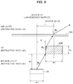
- FIG. 8 to FIG. 11 are diagrams for describing a method for setting the amount of misalignment L of the CF 33 a .
- FIG. 8 to FIG. 11 simulatively shows the luminescence section 24 of one light emitting element 10 , one CF 33 a provided to correspond to the light emitting element 10 (in the illustrated example, a CF 33 R), and the display surface 101 of the display device 1 .
- a case where the viewing angle of the focused-on pixel is ⁇ 0 means a case where, when emission light from the luminescence section 24 passes through the CF 33 R and other medium layers (the first member 51 , the protection film 31 , the planarizing film 32 , etc. described with reference to FIG. 2 ) and is emitted from the display surface 101 , light is emitted in a direction at an angle of ⁇ 0 from the direction perpendicular to the display surface 101 .
- the medium layers other than the CF 33 R contain a uniform material, for the sake of simplicity; if the refractive index of this material is denoted by n 1 , the refractive index of the CF 33 R is denoted by n 2 , and the refractive index of an air layer on the outside of the display surface 101 is denoted by n 0 , the emission angle ⁇ 1 of emission light from the luminescence section 24 (the angle of emission light with respect to the direction perpendicular to the luminescence surface of the luminescence section 24 ) when emission light from the display surface 101 has an angle of ⁇ 0 can be expressed by Mathematical Formula (1) below from the law of refraction.
- the amount of misalignment L of the CF 33 R for obtaining light with a viewing angle of ⁇ 0 on the display surface 101 may be set as a such a value that light emitted from the luminescence section 24 at an emission angle of ⁇ 1 passes through the CF 33 R and the other medium layers.
- medium layers such as the first member 51 and the protection film 31 exist immediately above the luminescence section 24 as described with reference to FIG.
- the amount of misalignment L of the CF 33 R for obtaining light with a viewing angle of ⁇ 0 on the display surface 101 may be set as such a value that emission light with an emission angle of ⁇ 1 from the luminescence section 24 passes through the CF 33 R.
- the amount of misalignment L of the CF 33 R is set as such a value that emission light with an emission angle of ⁇ 1 from the luminescence section 24 is incident on the lower surface of the CF 33 R
- the case where the value of the amount of misalignment L of the CF 33 R is largest is a case where emission light from the center of the luminescence surface of the luminescence section 24 is incident on an end of the lower surface of the CF 33 R on a side near to the luminescence section 24 .
- FIG. 1 the case where the value of the amount of misalignment L of the CF 33 R is largest is a case where emission light from the center of the luminescence surface of the luminescence section 24 is incident on an end of the lower surface of the CF 33 R on a side near to the luminescence section 24 .
- the width of the CF 33 R is denoted by w 2
- the distance in the stacking direction from the surface of the luminescence section 24 to the lower surface of the CF 33 R is denoted by g 1
- the distance in the horizontal plane from the luminescence position in the luminescence section 24 to the position where emission light is incident on the CF 33 R is denoted by d.
- the case where the value of the amount of misalignment L of the CF 33 R is smallest is a case where emission light from the center of the luminescence surface of the luminescence section 24 is incident on an end of the lower surface of the CF 33 R on a side far from the luminescence section 24 .
- the range of the amount of misalignment L of the CF 33 R is set more finely by further taking into account luminescence positions in the luminescence surface of the luminescence section 24 .
- the case where the value of the amount of misalignment L of the CF 33 R is largest is a case where emission light from a luminescence position of the luminescence surface of the luminescence section 24 nearest to the CF 33 R is incident on the lower surface of the CF 33 R.
- FIG. 10 shows the positional relationship between the luminescence section 24 and the CF 33 R and the locus of a light beam in such a case where emission light from a luminescence position of the luminescence surface of the luminescence section 24 nearest to the CF 33 R (in the illustrated example, the right end) is incident on the lower surface of the CF 33 R.
- FIG. 10 shows, as an example, the positional relationship between the luminescence section 24 and the CF 33 R and the locus of a light beam in a case where emission light from the luminescence section 24 is incident on an end of the lower surface of the CF 33 R on a side near to the luminescence section 24 (in the illustrated example, the left end), like in the case shown in FIG. 8 .
- the amount of misalignment L of the CF 33 R can be expressed by Mathematical Formula (5) below from geometric consideration.
- the width of the luminescence section 24 is denoted by w 1 .
- the case where the value of the amount of misalignment L of the CF 33 R is smallest is a case where emission light from a luminescence position of the luminescence surface of the luminescence section 24 farthest from the CF 33 R is incident on the lower surface of the CF 33 R.
- FIG. 11 shows the positional relationship between the luminescence section 24 and the CF 33 R and the locus of a light beam in such a case where emission light from a luminescence position of the luminescence surface of the luminescence section 24 farthest from the CF 33 R (in the illustrated example, the left end) is incident on the lower surface of the CF 33 R.
- FIG. 11 shows, as an example, the positional relationship between the luminescence section 24 and the CF 33 R and the locus of a light beam in a case where emission light from the luminescence section 24 is incident on an end of the lower surface of the CF 33 R on a side near to the luminescence section 24 (in the illustrated example, the left end), like in the case shown in FIG. 8 .
- the amount of misalignment L of the CF 33 R can be expressed by Mathematical Formula (6) below from geometric consideration.
- the range of values that the amount of misalignment L of the CF 33 R can take in order to obtain a viewing angle of ⁇ 0 for emission light from the display surface 101 can be expressed by Mathematical Formula (7) below;
- Mathematical Formula (7) a viewing angle of ⁇ 0 can be obtained for emission light from the display surface 101 .
- a transition region 201 in which the area of the CF 33 a is different from the area of another normal CF 33 a is provided in the CF layer 33 , as described with reference to FIG. 6 and FIG. 7 .
- the method for creating a relative misalignment between the light emitting element 10 and the CF 33 a is not limited to the method mentioned above, and may be other methods.
- FIG. 12 is a diagram for describing another method for creating a relative misalignment between the light emitting element 10 and the CF 33 a .
- FIG. 12 like in FIG. 3 and FIG. 7 , a cross-sectional structure in the stacking direction of a display device 1 a according to the present modification example is simplified, and only the first substrate 11 , the light emitting element 10 , the second member 52 , and the CF layer 33 are shown.
- the display device 1 a according to the present modification example has a similar configuration to the display device 1 according to the above embodiment except that the method for creating a relative misalignment between the light emitting element 10 and the CF 33 a is different. Therefore, in the following description regarding the present modification example, matters different from the above embodiment are mainly described, and a detailed description of matters different from the above embodiment is omitted.
- the inside of the display surface of the display device 1 a is divided into a plurality of regions, and the amount of misalignment L and the misalignment direction may be set for each region in accordance with the position in the display surface of the region.
- the transition region 207 is formed as a region in which the pitch with which light emitting elements 10 are arranged (that is, the pixel spacing) is narrower than a normal pitch of another region. Further, in the transition region 207 , the pixel spacing is adjusted such that the arrangement pitch of the light emitting element 10 is reduced on the misalignment side. Thereby, in region 205 , the center of the CF 33 a is placed to be shifted in the horizontal plane from the center of the luminescence surface of the luminescence section 24 by an amount of misalignment L>0 in the direction in which the arrangement pitch of the light emitting element 10 is reduced. Also between not-shown other regions, the amount of misalignment L and/or the misalignment direction can be changed between regions by providing a similar transition region 207 .
- the amount of misalignment L and the misalignment direction may be set not on a region basis but on a pixel basis, and the amount of misalignment L and the misalignment direction may be changed in a continuous manner between pixels in accordance with the position in the display surface of the pixel, like in the above embodiment.
- the misalignment direction of the CF 33 a may be only one of the horizontal direction and the vertical direction of the display surface 101 , or may be a two-dimensional arbitrary direction in the horizontal plane.
- a region in which the CF 33 a is not provided may be formed in the CF layer 33 .
- the inside of the display surface of the display device is divided into a plurality of regions, and the amount of misalignment L and the misalignment direction are set for each region in accordance with the position in the display surface of the region, a transition region between regions is formed as a region with a prescribed distance in which the CF 33 a is not provided.
- the center of the luminescence surface of the light emitting element 10 and the center of the CF 33 a in the horizontal plane are shifted between before and after the transition region by 1 ⁇ 3 of the arrangement pitch of the light emitting element 10 in the direction in which the region in which the CF 33 a is not provided is formed. That is, the amount of misalignment L and the misalignment direction can be changed between before and after the transition region.
- the reflector 53 is provided between pixels for luminance improvement (see FIG. 2 ).
- the present embodiment is not limited to this example, and the achievement of the object of improving the viewing angle characteristics does not necessarily requires the reflector 53 being provided.
- FIG. 13 is a diagram showing a configuration example of a display device 1 b according to a modification example in which the reflector 53 is not provided.
- a cross-sectional structure in the stacking direction of the display device 1 b according to the present modification example is simplified, and only the first substrate 11 , the light emitting element 10 , a second member 52 a , and the CF layer 33 are shown, like in FIG. 3 and FIG. 7 .
- the display device 1 b according to the present modification example has a similar configuration to the display device 1 according to the above embodiment except that the reflector 53 is not provided. Therefore, in the following description regarding the present modification example, matters different from the above embodiment are mainly described, and a detailed description of matters different from the above embodiment is omitted.
- a second member 52 a that is provided between pixels and functions as a pixel defining film that defines the pixel is provided in place of the second member 52 of the display device 1 according to the above embodiment.
- the second member 52 a is formed as a layer having a thinner film thickness than the second member 52 in the above embodiment.
- the area of the side wall of the opening of the second member 52 a which is a region immediately above the luminescence section of the light emitting element 10 , is not sufficiently ensured (that is, for a first member embedded in the opening of the second member 52 a , relations like those described above are not sufficiently ensured for the height, or the area of the light incidence surface or the light emitting surface), and the surface of the second member 52 a cannot function as a reflector. That is, the display device 1 b is a display device in which a reflector is not provided.
- the amount of misalignment L of the CF 33 a is set by prescribing conditions where emission light from the luminescence section 24 is incident on the lower surface of the CF 33 R.
- the present embodiment is not limited to this example.
- the amount of misalignment L of the CF 33 a may be set taking into account also a case where emission light from the luminescence section 24 is incident on the side surface of the CF 33 a.
- FIG. 14 is a diagram for describing a method for setting the amount of misalignment L of the CF 33 a taking into account also a case where emission light from the luminescence section 24 is incident on the side surface of the CF 33 a .
- FIG. 14 is a diagram for describing a method for setting the amount of misalignment L of the CF 33 a taking into account also a case where emission light from the luminescence section 24 is incident on the side surface of the CF 33 a .
- FIG. 8 to FIG. 11 FIG.
- FIG. 14 simulatively shows the luminescence section 24 of one light emitting element 10 provided in a display device according to the present modification example, one CF 33 a provided to correspond to the light emitting element 10 (in the illustrated example, a CF 33 R), and the display surface 101 of the display device. Further, medium layers are treated as layers containing a uniform material with a refractive index of n 2 .
- the thickness of the CF 33 R is denoted by h 2 ; within the distance d in the horizontal plane from the luminescence position in the luminescence section 24 to the position where emission light is incident on the CF 33 R, the length of a portion corresponding to the distance g 1 in the stacking direction from the surface of the luminescence section 24 to the lower surface of the CF 33 R is denoted by d 1 ; and within the distance d, the length of a portion corresponding to the thickness h 2 of the CF 33 R is denoted by w p .
- the upper limit value of the range that the amount of displacement L of the CF 33 R can take is made larger by taking into account also a case where emission light from the luminescence section 24 is incident on the side surface of the CF 33 a .
- FIG. 14 it is assumed that light is emitted from one point of the center of the luminescence surface of the luminescence section 24 ; however, if also a case where light is emitted from other parts in the luminescence surface is taken into account like in the consideration in (3.
- amount of misalignment of CF the range that the amount of displacement L of the CF 33 R can take can be expressed by Mathematical Formula (9) below, in the end.
- an optimum amount of misalignment and an optimum misalignment direction of the CF 33 a may be found in a trial and error manner by repeatedly performing an optical simulation and an experiment using a sample fabricated on the basis of the simulation result, as another method for setting the amount of misalignment L of the CF 33 a.
- FIG. 15 is a diagram showing an external appearance of a smartphone that is an example of the electronic apparatus in which the display devices according to the present embodiment and the modification examples can be used.
- a smartphone 301 includes an operation section 303 that includes a button and accepts an operation input by the user and a display section 305 that displays various pieces of information.
- the display section 305 may include any of the display devices according to the present embodiment and the modification examples.
- FIG. 16 and FIG. 17 are diagrams showing external appearances of a digital camera that is another example of the electronic apparatus in which the display devices according to the present embodiment and the modification examples can be used.
- FIG. 16 shows an external appearance of a digital camera 311 as seen from the front side (the subject side)
- FIG. 17 shows an external appearance of the digital camera 311 as seen from the rear side.
- the digital camera 311 includes a main body section (camera body) 313 , a replaceable lens unit 315 , a grip section 317 that is gripped by the user during photographing, a monitor 319 that displays various pieces of information, and an EVF 321 that displays a through image that is observed by the user during photographing.
- the monitor 319 and the EVF 321 may include any of the display devices according to the present embodiment and the modification examples.
- FIG. 18 is a diagram showing an external appearance of an HMD that is another example of the electronic apparatus in which the display devices according to the present embodiment and the modification examples can be used.
- an HMD 331 includes an eyeglass-type display section 333 that displays various pieces of information and ear-fixing sections 335 that are fixed to the user's ears during wearing.
- the display section 333 may include any of the display devices according to the present embodiment and the modification examples.
- the electronic apparatus in which the display devices according to the present embodiment and the modification examples can be used is not limited to those described above as examples, and the display device can be used for display devices that are mounted on electronic apparatuses in all fields that perform display on the basis of an image signal inputted from the outside or an image signal generated in the inside, such as a television device, an electronic book, a PDA, a notebook PC, a video camera, an HMD, and a game apparatus.
- the following experiment was performed in order to verify the effect of improving the viewing angle characteristics by the display device 1 according to the present embodiment described above.
- a sample of a display device having a configuration similar to the configuration of the display device 1 according to the present embodiment shown in FIG. 2 was produced, the display device was actually driven, and differences in chromaticity in accordance with the viewing angle of light emitted from the display surface were measured.
- a configuration in which sub-pixels of four colors of red, green, blue, and white were combined as one pixel was used as a luminescence pixel (that is, three colors of red, green, and blue were used as CFs).
- the spacing between pixels each including sub-pixels of four colors was set to 6.8 ⁇ m. Further, the film thickness of the CF was set to 2 ⁇ m.
- a desired viewing angle on the display surface was set to 30°, in the region mentioned above in which a relative misalignment between the light emitting element and the CF was created, the misalignment direction of the CF was set to the same direction as the direction in which the viewing angle mentioned above was intended to be obtained.
- the display device was actually driven, and the u′v′ chromaticity point of each of red, green, and blue was measured for emission light from the display surface, using a spectrophotometer (CS-2000, manufactured by Konica Minolta, Inc.).
- the u′v′ chromaticity point was measured in each of a position corresponding to a viewing angle of 30° for emission light from a region in which a relative misalignment between the light emitting element and the CF was created (a misalignment-created region), a position corresponding to a viewing angle of 30° for emission light from a region in which a relative misalignment between the light emitting element and the CF was not created (a misalignment-not-created region), and a position corresponding to a viewing angle of 0° for emission light from the misalignment-not-created region.
- Table 1 The results are shown in Table 1 below.
- the display device is an organic EL display
- the present disclosure is not limited to this example.
- the display device that is an object of the present disclosure may be various display devices as long as they are display devices that can achieve color display by using CFs, such as a liquid crystal display, a plasma display, and an electronic paper device.
- the light emitting section is a part that is included in each pixel of the display device and that emits light toward the outside.
- the light emitting section corresponds to a light emitting element.
- the light emitting section corresponds to a region corresponding to one pixel of a liquid crystal panel.
- the light emitting section corresponds to a region corresponding to one discharge cell of a plasma display panel.
- present technology may also be configured as below.
- a display device including:
- a color filter provided on the light emitting section to correspond to each of the plurality of light emitting sections
- the light emitting sections and the color filters are arranged such that, in at least a partial region in a display surface, a relative misalignment between a center of a luminescence surface of the light emitting section and a center of the color filter corresponding to the light emitting section is created in a plane perpendicular to a stacking direction.
- the display device according to any one of (1) to (4),
- a pitch with which the light emitting sections are arranged on the substrate is different in at least a partial region from the pitch in another region, and thereby the relative misalignment is created.
- an amount of misalignment in the relative misalignment and a misalignment direction of the center of the color filter corresponding to the light emitting section with respect to the center of the luminescence surface of the light emitting section in the plane perpendicular to the stacking direction are set in accordance with a viewing angle required of a pixel including the light emitting section and the color filter in which the relative misalignment is created.
- a misalignment direction of the center of the color filter corresponding to the light emitting section with respect to the center of the luminescence surface of the light emitting section in the plane perpendicular to the stacking direction is a direction from a center of the display surface toward a position where the light emitting section and the color filter in which the relative misalignment is created exist in the display surface.
- the display device according to any one of (1) to (8), further including:
- a first member provided immediately above the light emitting section, having a substantially truncated conical or pyramidal shape in which a cross-sectional area in an in-plane direction perpendicular to the stacking direction gradually increases with proximity to a top, and configured to propagate emission light from the light emitting section;
- a refractive index of the first member is larger than a refractive index of the second member.
- the light emitting section is a light emitting element including an organic light emitting diode
- the display device is an organic EL display.
- An electronic apparatus including:
- a display device configured to perform display on a basis of an image signal
- the display device includes
- the light emitting sections and the color filters are arranged such that, in at least a partial region in a display surface, a relative misalignment between a center of a luminescence surface of the light emitting section and a center of the color filter corresponding to the light emitting section is created in a plane perpendicular to a stacking direction.
Abstract
Description
| TABLE 1 | ||||
| Luminescent | ||||
| color | u′ | v′ | ||
| Misalignment-created region (L = 0.6 um) | Red | 0.39 | 0.54 |
| Measured point: a position corresponding | Green | 0.15 | 0.57 |
| to a viewing angle of 30° | Blue | 0.18 | 0.21 |
| Misalignment-not-created region (L = 0) | Red | 0.35 | 0.54 |
| Measured point: a position corresponding | Green | 0.15 | 0.56 |
| to a viewing angle of 30° | Blue | 0.18 | 0.32 |
| Misalignment-not-created region (L = 0) | Red | 0.39 | 0.54 |
| Measured point: a position corresponding | Green | 0.14 | 0.57 |
| to a viewing angle of 0° | Blue | 0.18 | 0.20 |
-
- a plurality of light emitting sections formed on a substrate, and
- a color filter provided on the light emitting section to correspond to each of the plurality of light emitting sections, and
- 1, 1 a, 1 b display device
- 10 light emitting element
- 11 first substrate
- 15 TFT
- 21 first electrode
- 22 second electrode
- 23 organic layer
- 24 luminescence section
- 25 opening
- 31 protection film
- 32 planarizing film
- 33 CF layer
- 33R, 33G. 33B CF
- 34 second substrate
- 35 sealing resin film
- 51 first member
- 52 second member
- 53 reflector
- 101 display surface
- 301 smartphone (electronic apparatus)
- 311 digital camera (electronic apparatus)
- 331 HMD (electronic apparatus)
Claims (18)
Applications Claiming Priority (3)
| Application Number | Priority Date | Filing Date | Title |
|---|---|---|---|
| JP2016069879 | 2016-03-31 | ||
| JP2016-069879 | 2016-03-31 | ||
| PCT/JP2017/008961 WO2017169563A1 (en) | 2016-03-31 | 2017-03-07 | Display device and electronic apparatus |
Related Parent Applications (1)
| Application Number | Title | Priority Date | Filing Date |
|---|---|---|---|
| PCT/JP2017/008961 A-371-Of-International WO2017169563A1 (en) | 2016-03-31 | 2017-03-07 | Display device and electronic apparatus |
Related Child Applications (1)
| Application Number | Title | Priority Date | Filing Date |
|---|---|---|---|
| US16/854,309 Continuation US11143802B2 (en) | 2016-03-31 | 2020-04-21 | Display device and electronic apparatus |
Publications (2)
| Publication Number | Publication Date |
|---|---|
| US20190056543A1 US20190056543A1 (en) | 2019-02-21 |
| US10684401B2 true US10684401B2 (en) | 2020-06-16 |
Family
ID=59964062
Family Applications (4)
| Application Number | Title | Priority Date | Filing Date |
|---|---|---|---|
| US16/080,089 Active 2037-03-11 US10684401B2 (en) | 2016-03-31 | 2017-03-07 | Display device and electronic apparatus |
| US16/854,309 Active US11143802B2 (en) | 2016-03-31 | 2020-04-21 | Display device and electronic apparatus |
| US17/465,707 Active US11703619B2 (en) | 2016-03-31 | 2021-09-02 | Display device and electronic apparatus |
| US18/323,070 Pending US20240027664A1 (en) | 2016-03-31 | 2023-05-24 | Display device and electronic apparatus |
Family Applications After (3)
| Application Number | Title | Priority Date | Filing Date |
|---|---|---|---|
| US16/854,309 Active US11143802B2 (en) | 2016-03-31 | 2020-04-21 | Display device and electronic apparatus |
| US17/465,707 Active US11703619B2 (en) | 2016-03-31 | 2021-09-02 | Display device and electronic apparatus |
| US18/323,070 Pending US20240027664A1 (en) | 2016-03-31 | 2023-05-24 | Display device and electronic apparatus |
Country Status (6)
| Country | Link |
|---|---|
| US (4) | US10684401B2 (en) |
| JP (2) | JP6813022B2 (en) |
| KR (2) | KR102457437B1 (en) |
| CN (4) | CN110120405B (en) |
| DE (1) | DE112017001717B4 (en) |
| WO (1) | WO2017169563A1 (en) |
Cited By (1)
| Publication number | Priority date | Publication date | Assignee | Title |
|---|---|---|---|---|
| US20230006176A1 (en) * | 2018-03-06 | 2023-01-05 | Sony Semiconductor Solutions Corporation | Light emitting element unit |
Families Citing this family (12)
| Publication number | Priority date | Publication date | Assignee | Title |
|---|---|---|---|---|
| CN110120405B (en) * | 2016-03-31 | 2023-04-11 | 索尼公司 | Display device |
| TWI679627B (en) * | 2018-06-28 | 2019-12-11 | 友達光電股份有限公司 | Display panel |
| CN109524442B (en) * | 2018-11-29 | 2020-06-19 | 京东方科技集团股份有限公司 | Organic light emitting diode display substrate, preparation method thereof and display device |
| KR20210098446A (en) | 2018-11-30 | 2021-08-10 | 소니그룹주식회사 | display device |
| JP7353834B2 (en) * | 2019-07-12 | 2023-10-02 | キヤノン株式会社 | Display devices and display systems |
| CN111025660B (en) * | 2019-12-31 | 2022-04-19 | 合肥视涯技术有限公司 | Display panel and near-to-eye display device |
| JP6971438B2 (en) | 2020-01-29 | 2021-11-24 | セイコーエプソン株式会社 | Electro-optics and electronics |
| JP2021124538A (en) | 2020-01-31 | 2021-08-30 | キヤノン株式会社 | Image observation device |
| JP2021136207A (en) | 2020-02-28 | 2021-09-13 | キヤノン株式会社 | Organic light emitting device, display device, electronic device, lighting device, and mobile body |
| JP7458847B2 (en) * | 2020-03-24 | 2024-04-01 | キヤノン株式会社 | Display and electronic devices |
| JP7198250B2 (en) * | 2020-10-12 | 2022-12-28 | キヤノン株式会社 | Display device |
| WO2023106082A1 (en) * | 2021-12-10 | 2023-06-15 | ソニーセミコンダクタソリューションズ株式会社 | Display element and display device |
Citations (7)
| Publication number | Priority date | Publication date | Assignee | Title |
|---|---|---|---|---|
| JPH1138426A (en) | 1997-07-17 | 1999-02-12 | Mitsubishi Electric Corp | Liquid crystal display device |
| JP2011040352A (en) | 2009-08-18 | 2011-02-24 | Sony Corp | Display device |
| JP2014067576A (en) | 2012-09-26 | 2014-04-17 | Sony Corp | Display device and electronic apparatus |
| WO2014141842A1 (en) | 2013-03-15 | 2014-09-18 | ソニー株式会社 | Display device and method for manufacturing same |
| US20150070552A1 (en) * | 2013-09-09 | 2015-03-12 | Himax Imaging Limited | Image sensor with convex substances and notches which change in accordance with distances to image sensor center |
| JP2017009625A (en) | 2015-06-16 | 2017-01-12 | ソニー株式会社 | Display device, manufacturing method therefor, and electronic device |
| US20170309844A1 (en) * | 2014-09-30 | 2017-10-26 | Toray Industries, Inc. | Substrate for display, color filter using the same and method for the production thereof, organic el element and method for the production thereof, and flexible organic el display (as amended) |
Family Cites Families (31)
| Publication number | Priority date | Publication date | Assignee | Title |
|---|---|---|---|---|
| JPH10333131A (en) * | 1996-12-17 | 1998-12-18 | Matsushita Electric Ind Co Ltd | Display panel, manufacture of display panel, driving method for display panel, defect correcting method for display panel, and display device using display panel |
| JP4011292B2 (en) * | 2001-01-15 | 2007-11-21 | 株式会社日立製作所 | LIGHT EMITTING ELEMENT AND DISPLAY DEVICE |
| JP4182467B2 (en) * | 2001-12-27 | 2008-11-19 | セイコーエプソン株式会社 | Circuit board, electro-optical device and electronic apparatus |
| JP4094919B2 (en) * | 2002-07-18 | 2008-06-04 | 東北パイオニア株式会社 | Organic light emitting display |
| JP3788448B2 (en) * | 2003-07-18 | 2006-06-21 | セイコーエプソン株式会社 | Color filter substrate, transflective substrate, color filter substrate manufacturing method, electro-optical device, and electronic apparatus |
| GB2405545A (en) * | 2003-08-30 | 2005-03-02 | Sharp Kk | Multiple view directional display with parallax optic having colour filters. |
| KR20050068441A (en) * | 2003-12-30 | 2005-07-05 | 엘지.필립스 엘시디 주식회사 | The organic electro-luminescence device and method for fabricating of the same |
| JP2006019179A (en) * | 2004-07-02 | 2006-01-19 | Dainippon Printing Co Ltd | Organic el element |
| US7436113B2 (en) * | 2005-04-25 | 2008-10-14 | Eastman Kodak Company | Multicolor OLED displays |
| JP4201019B2 (en) * | 2006-05-30 | 2008-12-24 | エプソンイメージングデバイス株式会社 | Liquid crystal display device and method of manufacturing liquid crystal display device |
| US20080137008A1 (en) * | 2006-12-06 | 2008-06-12 | General Electric Company | Color tunable oled illumination display and method for controlled display illumination |
| US7741770B2 (en) * | 2007-10-05 | 2010-06-22 | Global Oled Technology Llc | LED device having improved light output |
| JP5650918B2 (en) | 2010-03-26 | 2015-01-07 | 株式会社ジャパンディスプレイ | Image display device |
| JP5459142B2 (en) * | 2010-08-11 | 2014-04-02 | セイコーエプソン株式会社 | ORGANIC EL DEVICE, METHOD FOR MANUFACTURING ORGANIC EL DEVICE, AND ELECTRONIC DEVICE |
| JP2013175433A (en) * | 2012-01-24 | 2013-09-05 | Canon Inc | Display device |
| JP6082907B2 (en) | 2012-02-17 | 2017-02-22 | 株式会社Joled | Display device and manufacturing method of display device |
| JP6015481B2 (en) * | 2012-03-28 | 2016-10-26 | Jsr株式会社 | Color filter, organic EL display element, and coloring composition |
| CA2879220A1 (en) | 2012-07-23 | 2014-01-30 | Dow Agrosciences Llc | Kernel counter |
| KR102014885B1 (en) * | 2012-12-26 | 2019-08-28 | 삼성디스플레이 주식회사 | Organic light emitting display and manufacturing method thereof |
| KR102082780B1 (en) * | 2013-01-10 | 2020-03-02 | 삼성디스플레이 주식회사 | Organic light emitting display apparatus and method of manufacturing thereof |
| JP2014141842A (en) * | 2013-01-25 | 2014-08-07 | Saicon Industry Co Ltd | Solar battery panel installation structure and method of forming the same |
| JP2014229566A (en) * | 2013-05-24 | 2014-12-08 | ソニー株式会社 | Light-emitting element, display device, and illuminating device |
| JP2015002075A (en) * | 2013-06-14 | 2015-01-05 | ソニー株式会社 | Light emitting element, display device and lighting system |
| KR102109741B1 (en) * | 2013-10-02 | 2020-05-12 | 엘지디스플레이 주식회사 | Organic light emitting display device |
| KR102159830B1 (en) * | 2013-12-30 | 2020-09-24 | 엘지디스플레이 주식회사 | Display device |
| JP2015149231A (en) * | 2014-02-07 | 2015-08-20 | 株式会社ジャパンディスプレイ | organic EL display device |
| JP6269387B2 (en) * | 2014-08-21 | 2018-01-31 | セイコーエプソン株式会社 | Display device and electronic device |
| US9910265B1 (en) * | 2015-06-29 | 2018-03-06 | Amazon Technologies, Inc. | Electrowetting display having misaligned color filters |
| JP2017057387A (en) | 2015-09-17 | 2017-03-23 | 矢崎エナジーシステム株式会社 | Non-halogen flame retardant resin composition, wire and cable using the same |
| WO2017057387A1 (en) * | 2015-09-30 | 2017-04-06 | シャープ株式会社 | Display device |
| CN110120405B (en) * | 2016-03-31 | 2023-04-11 | 索尼公司 | Display device |
-
2017
- 2017-03-07 CN CN201910320067.6A patent/CN110120405B/en active Active
- 2017-03-07 KR KR1020217032807A patent/KR102457437B1/en active IP Right Grant
- 2017-03-07 WO PCT/JP2017/008961 patent/WO2017169563A1/en active Application Filing
- 2017-03-07 US US16/080,089 patent/US10684401B2/en active Active
- 2017-03-07 JP JP2018508880A patent/JP6813022B2/en active Active
- 2017-03-07 CN CN202110405083.2A patent/CN113130614A/en active Pending
- 2017-03-07 DE DE112017001717.3T patent/DE112017001717B4/en active Active
- 2017-03-07 CN CN201780019568.XA patent/CN108885848B/en active Active
- 2017-03-07 CN CN202110405295.0A patent/CN113130615A/en active Pending
- 2017-03-07 KR KR1020187023994A patent/KR102318464B1/en active IP Right Grant
-
2020
- 2020-04-21 US US16/854,309 patent/US11143802B2/en active Active
- 2020-12-17 JP JP2020208974A patent/JP7047889B2/en active Active
-
2021
- 2021-09-02 US US17/465,707 patent/US11703619B2/en active Active
-
2023
- 2023-05-24 US US18/323,070 patent/US20240027664A1/en active Pending
Patent Citations (7)
| Publication number | Priority date | Publication date | Assignee | Title |
|---|---|---|---|---|
| JPH1138426A (en) | 1997-07-17 | 1999-02-12 | Mitsubishi Electric Corp | Liquid crystal display device |
| JP2011040352A (en) | 2009-08-18 | 2011-02-24 | Sony Corp | Display device |
| JP2014067576A (en) | 2012-09-26 | 2014-04-17 | Sony Corp | Display device and electronic apparatus |
| WO2014141842A1 (en) | 2013-03-15 | 2014-09-18 | ソニー株式会社 | Display device and method for manufacturing same |
| US20150070552A1 (en) * | 2013-09-09 | 2015-03-12 | Himax Imaging Limited | Image sensor with convex substances and notches which change in accordance with distances to image sensor center |
| US20170309844A1 (en) * | 2014-09-30 | 2017-10-26 | Toray Industries, Inc. | Substrate for display, color filter using the same and method for the production thereof, organic el element and method for the production thereof, and flexible organic el display (as amended) |
| JP2017009625A (en) | 2015-06-16 | 2017-01-12 | ソニー株式会社 | Display device, manufacturing method therefor, and electronic device |
Cited By (1)
| Publication number | Priority date | Publication date | Assignee | Title |
|---|---|---|---|---|
| US20230006176A1 (en) * | 2018-03-06 | 2023-01-05 | Sony Semiconductor Solutions Corporation | Light emitting element unit |
Also Published As
| Publication number | Publication date |
|---|---|
| JP7047889B2 (en) | 2022-04-05 |
| US20210063620A1 (en) | 2021-03-04 |
| KR20210127800A (en) | 2021-10-22 |
| US20240027664A1 (en) | 2024-01-25 |
| JP6813022B2 (en) | 2021-01-13 |
| KR102318464B1 (en) | 2021-10-28 |
| US20220057554A1 (en) | 2022-02-24 |
| CN113130614A (en) | 2021-07-16 |
| US11143802B2 (en) | 2021-10-12 |
| US11703619B2 (en) | 2023-07-18 |
| CN110120405B (en) | 2023-04-11 |
| KR102457437B1 (en) | 2022-10-24 |
| DE112017001717T5 (en) | 2018-12-20 |
| JP2021056527A (en) | 2021-04-08 |
| CN108885848A (en) | 2018-11-23 |
| CN108885848B (en) | 2021-05-04 |
| WO2017169563A1 (en) | 2017-10-05 |
| DE112017001717B4 (en) | 2019-12-24 |
| KR20180123016A (en) | 2018-11-14 |
| CN113130615A (en) | 2021-07-16 |
| CN110120405A (en) | 2019-08-13 |
| US20190056543A1 (en) | 2019-02-21 |
| JPWO2017169563A1 (en) | 2019-02-14 |
Similar Documents
| Publication | Publication Date | Title |
|---|---|---|
| US11703619B2 (en) | Display device and electronic apparatus | |
| US11545649B2 (en) | Display device and electronic apparatus with relative misalignment between pixel and color filter | |
| US11107372B2 (en) | Display device and electronic apparatus | |
| US11769773B2 (en) | Display device, electronic device, and method of manufacturing display device with substrate including light emitting elements adhered to substrate including microlens array | |
| US10181500B2 (en) | Display device and method of manufacturing the same | |
| JP7014186B2 (en) | Display devices, electronic devices, and methods for manufacturing display devices. | |
| JP2013258021A (en) | Display device | |
| KR20200002342A (en) | Display device | |
| CN116583895A (en) | Display device and electronic apparatus | |
| WO2023095662A1 (en) | Display device and method for producing same, and electronic device |
Legal Events
| Date | Code | Title | Description |
|---|---|---|---|
| AS | Assignment |
Owner name: SONY CORPORATION, JAPAN Free format text: ASSIGNMENT OF ASSIGNORS INTEREST;ASSIGNOR:UEDA, DAISUKE;REEL/FRAME:047470/0768 Effective date: 20180730 |
|
| FEPP | Fee payment procedure |
Free format text: ENTITY STATUS SET TO UNDISCOUNTED (ORIGINAL EVENT CODE: BIG.); ENTITY STATUS OF PATENT OWNER: LARGE ENTITY |
|
| STPP | Information on status: patent application and granting procedure in general |
Free format text: DOCKETED NEW CASE - READY FOR EXAMINATION |
|
| STPP | Information on status: patent application and granting procedure in general |
Free format text: NON FINAL ACTION MAILED |
|
| STPP | Information on status: patent application and granting procedure in general |
Free format text: RESPONSE TO NON-FINAL OFFICE ACTION ENTERED AND FORWARDED TO EXAMINER |
|
| STPP | Information on status: patent application and granting procedure in general |
Free format text: NOTICE OF ALLOWANCE MAILED -- APPLICATION RECEIVED IN OFFICE OF PUBLICATIONS |
|
| STPP | Information on status: patent application and granting procedure in general |
Free format text: PUBLICATIONS -- ISSUE FEE PAYMENT VERIFIED |
|
| STCF | Information on status: patent grant |
Free format text: PATENTED CASE |
|
| AS | Assignment |
Owner name: SONY GROUP CORPORATION, JAPAN Free format text: CHANGE OF NAME;ASSIGNOR:SONY CORPORATION;REEL/FRAME:057392/0183 Effective date: 20210401 |
|
| AS | Assignment |
Owner name: SONY GROUP CORPORATION, JAPAN Free format text: CHANGE OF NAME;ASSIGNOR:SONY CORPORATION;REEL/FRAME:057394/0038 Effective date: 20210401 |
|
| MAFP | Maintenance fee payment |
Free format text: PAYMENT OF MAINTENANCE FEE, 4TH YEAR, LARGE ENTITY (ORIGINAL EVENT CODE: M1551); ENTITY STATUS OF PATENT OWNER: LARGE ENTITY Year of fee payment: 4 |