US10678080B2 - Display device - Google Patents
Display device Download PDFInfo
- Publication number
- US10678080B2 US10678080B2 US16/167,778 US201816167778A US10678080B2 US 10678080 B2 US10678080 B2 US 10678080B2 US 201816167778 A US201816167778 A US 201816167778A US 10678080 B2 US10678080 B2 US 10678080B2
- Authority
- US
- United States
- Prior art keywords
- display panel
- cover
- panel
- display device
- disposed
- Prior art date
- Legal status (The legal status is an assumption and is not a legal conclusion. Google has not performed a legal analysis and makes no representation as to the accuracy of the status listed.)
- Active
Links
Images


Classifications
-
- G—PHYSICS
- G02—OPTICS
- G02F—OPTICAL DEVICES OR ARRANGEMENTS FOR THE CONTROL OF LIGHT BY MODIFICATION OF THE OPTICAL PROPERTIES OF THE MEDIA OF THE ELEMENTS INVOLVED THEREIN; NON-LINEAR OPTICS; FREQUENCY-CHANGING OF LIGHT; OPTICAL LOGIC ELEMENTS; OPTICAL ANALOGUE/DIGITAL CONVERTERS
- G02F1/00—Devices or arrangements for the control of the intensity, colour, phase, polarisation or direction of light arriving from an independent light source, e.g. switching, gating or modulating; Non-linear optics
- G02F1/01—Devices or arrangements for the control of the intensity, colour, phase, polarisation or direction of light arriving from an independent light source, e.g. switching, gating or modulating; Non-linear optics for the control of the intensity, phase, polarisation or colour
- G02F1/13—Devices or arrangements for the control of the intensity, colour, phase, polarisation or direction of light arriving from an independent light source, e.g. switching, gating or modulating; Non-linear optics for the control of the intensity, phase, polarisation or colour based on liquid crystals, e.g. single liquid crystal display cells
- G02F1/133—Constructional arrangements; Operation of liquid crystal cells; Circuit arrangements
- G02F1/1333—Constructional arrangements; Manufacturing methods
- G02F1/133308—Support structures for LCD panels, e.g. frames or bezels
-
- G—PHYSICS
- G02—OPTICS
- G02F—OPTICAL DEVICES OR ARRANGEMENTS FOR THE CONTROL OF LIGHT BY MODIFICATION OF THE OPTICAL PROPERTIES OF THE MEDIA OF THE ELEMENTS INVOLVED THEREIN; NON-LINEAR OPTICS; FREQUENCY-CHANGING OF LIGHT; OPTICAL LOGIC ELEMENTS; OPTICAL ANALOGUE/DIGITAL CONVERTERS
- G02F1/00—Devices or arrangements for the control of the intensity, colour, phase, polarisation or direction of light arriving from an independent light source, e.g. switching, gating or modulating; Non-linear optics
- G02F1/01—Devices or arrangements for the control of the intensity, colour, phase, polarisation or direction of light arriving from an independent light source, e.g. switching, gating or modulating; Non-linear optics for the control of the intensity, phase, polarisation or colour
- G02F1/13—Devices or arrangements for the control of the intensity, colour, phase, polarisation or direction of light arriving from an independent light source, e.g. switching, gating or modulating; Non-linear optics for the control of the intensity, phase, polarisation or colour based on liquid crystals, e.g. single liquid crystal display cells
- G02F1/133—Constructional arrangements; Operation of liquid crystal cells; Circuit arrangements
- G02F1/1333—Constructional arrangements; Manufacturing methods
- G02F1/133308—Support structures for LCD panels, e.g. frames or bezels
- G02F1/133314—Back frames
-
- G—PHYSICS
- G02—OPTICS
- G02F—OPTICAL DEVICES OR ARRANGEMENTS FOR THE CONTROL OF LIGHT BY MODIFICATION OF THE OPTICAL PROPERTIES OF THE MEDIA OF THE ELEMENTS INVOLVED THEREIN; NON-LINEAR OPTICS; FREQUENCY-CHANGING OF LIGHT; OPTICAL LOGIC ELEMENTS; OPTICAL ANALOGUE/DIGITAL CONVERTERS
- G02F1/00—Devices or arrangements for the control of the intensity, colour, phase, polarisation or direction of light arriving from an independent light source, e.g. switching, gating or modulating; Non-linear optics
- G02F1/01—Devices or arrangements for the control of the intensity, colour, phase, polarisation or direction of light arriving from an independent light source, e.g. switching, gating or modulating; Non-linear optics for the control of the intensity, phase, polarisation or colour
- G02F1/13—Devices or arrangements for the control of the intensity, colour, phase, polarisation or direction of light arriving from an independent light source, e.g. switching, gating or modulating; Non-linear optics for the control of the intensity, phase, polarisation or colour based on liquid crystals, e.g. single liquid crystal display cells
- G02F1/133—Constructional arrangements; Operation of liquid crystal cells; Circuit arrangements
- G02F1/1333—Constructional arrangements; Manufacturing methods
- G02F1/133308—Support structures for LCD panels, e.g. frames or bezels
- G02F1/133317—Intermediate frames, e.g. between backlight housing and front frame
-
- G—PHYSICS
- G02—OPTICS
- G02F—OPTICAL DEVICES OR ARRANGEMENTS FOR THE CONTROL OF LIGHT BY MODIFICATION OF THE OPTICAL PROPERTIES OF THE MEDIA OF THE ELEMENTS INVOLVED THEREIN; NON-LINEAR OPTICS; FREQUENCY-CHANGING OF LIGHT; OPTICAL LOGIC ELEMENTS; OPTICAL ANALOGUE/DIGITAL CONVERTERS
- G02F1/00—Devices or arrangements for the control of the intensity, colour, phase, polarisation or direction of light arriving from an independent light source, e.g. switching, gating or modulating; Non-linear optics
- G02F1/01—Devices or arrangements for the control of the intensity, colour, phase, polarisation or direction of light arriving from an independent light source, e.g. switching, gating or modulating; Non-linear optics for the control of the intensity, phase, polarisation or colour
- G02F1/13—Devices or arrangements for the control of the intensity, colour, phase, polarisation or direction of light arriving from an independent light source, e.g. switching, gating or modulating; Non-linear optics for the control of the intensity, phase, polarisation or colour based on liquid crystals, e.g. single liquid crystal display cells
- G02F1/133—Constructional arrangements; Operation of liquid crystal cells; Circuit arrangements
- G02F1/1333—Constructional arrangements; Manufacturing methods
- G02F1/133388—Constructional arrangements; Manufacturing methods with constructional differences between the display region and the peripheral region
-
- G—PHYSICS
- G02—OPTICS
- G02F—OPTICAL DEVICES OR ARRANGEMENTS FOR THE CONTROL OF LIGHT BY MODIFICATION OF THE OPTICAL PROPERTIES OF THE MEDIA OF THE ELEMENTS INVOLVED THEREIN; NON-LINEAR OPTICS; FREQUENCY-CHANGING OF LIGHT; OPTICAL LOGIC ELEMENTS; OPTICAL ANALOGUE/DIGITAL CONVERTERS
- G02F1/00—Devices or arrangements for the control of the intensity, colour, phase, polarisation or direction of light arriving from an independent light source, e.g. switching, gating or modulating; Non-linear optics
- G02F1/01—Devices or arrangements for the control of the intensity, colour, phase, polarisation or direction of light arriving from an independent light source, e.g. switching, gating or modulating; Non-linear optics for the control of the intensity, phase, polarisation or colour
- G02F1/13—Devices or arrangements for the control of the intensity, colour, phase, polarisation or direction of light arriving from an independent light source, e.g. switching, gating or modulating; Non-linear optics for the control of the intensity, phase, polarisation or colour based on liquid crystals, e.g. single liquid crystal display cells
- G02F1/133—Constructional arrangements; Operation of liquid crystal cells; Circuit arrangements
- G02F1/1333—Constructional arrangements; Manufacturing methods
- G02F1/1335—Structural association of cells with optical devices, e.g. polarisers or reflectors
- G02F1/133509—Filters, e.g. light shielding masks
- G02F1/133512—Light shielding layers, e.g. black matrix
-
- G—PHYSICS
- G02—OPTICS
- G02F—OPTICAL DEVICES OR ARRANGEMENTS FOR THE CONTROL OF LIGHT BY MODIFICATION OF THE OPTICAL PROPERTIES OF THE MEDIA OF THE ELEMENTS INVOLVED THEREIN; NON-LINEAR OPTICS; FREQUENCY-CHANGING OF LIGHT; OPTICAL LOGIC ELEMENTS; OPTICAL ANALOGUE/DIGITAL CONVERTERS
- G02F1/00—Devices or arrangements for the control of the intensity, colour, phase, polarisation or direction of light arriving from an independent light source, e.g. switching, gating or modulating; Non-linear optics
- G02F1/01—Devices or arrangements for the control of the intensity, colour, phase, polarisation or direction of light arriving from an independent light source, e.g. switching, gating or modulating; Non-linear optics for the control of the intensity, phase, polarisation or colour
- G02F1/13—Devices or arrangements for the control of the intensity, colour, phase, polarisation or direction of light arriving from an independent light source, e.g. switching, gating or modulating; Non-linear optics for the control of the intensity, phase, polarisation or colour based on liquid crystals, e.g. single liquid crystal display cells
- G02F1/133—Constructional arrangements; Operation of liquid crystal cells; Circuit arrangements
- G02F1/1333—Constructional arrangements; Manufacturing methods
- G02F1/1345—Conductors connecting electrodes to cell terminals
-
- G—PHYSICS
- G06—COMPUTING OR CALCULATING; COUNTING
- G06F—ELECTRIC DIGITAL DATA PROCESSING
- G06F1/00—Details not covered by groups G06F3/00 - G06F13/00 and G06F21/00
- G06F1/16—Constructional details or arrangements
- G06F1/1601—Constructional details related to the housing of computer displays, e.g. of CRT monitors, of flat displays
-
- G—PHYSICS
- G06—COMPUTING OR CALCULATING; COUNTING
- G06F—ELECTRIC DIGITAL DATA PROCESSING
- G06F1/00—Details not covered by groups G06F3/00 - G06F13/00 and G06F21/00
- G06F1/16—Constructional details or arrangements
- G06F1/1613—Constructional details or arrangements for portable computers
- G06F1/1633—Constructional details or arrangements of portable computers not specific to the type of enclosures covered by groups G06F1/1615 - G06F1/1626
- G06F1/1637—Details related to the display arrangement, including those related to the mounting of the display in the housing
-
- G02F2001/133388—
Definitions
- Embodiments of the present disclosure relate to a display device. More particularly, embodiments relate to a display device having a thin thickness.
- a flat panel display device which replaces a cathode-ray tube display device, is being developed to achieve light weight, low power consumption, and a slim profile.
- a flat display device may be divided into a light emitting type and a light receiving type.
- a light emitting type may include a Plasma Display Panel (PDP) and an Organic Light Emitting Diode (OLED).
- a light receiving type may include a Liquid Crystal Display (LCD).
- a display device which uses the Organic Light Emitting Diode, is superior in brightness and viewing angles in comparison to the Liquid Crystal Display. Further, the Display Device using the Organic Light Emitting Diode does not require a backlight unit, thereby accomplishing a slim profile.
- a display device includes a display panel, a side cover, and a black matrix.
- the display panel may have an active area to display an image, and an inactive area provided with a disposed pattern to apply an electrical signal to the active area.
- the side cover may have a peripheral frame, and a support frame.
- the peripheral frame may be disposed at an outer portion of the display panel to form a side portion exterior of the display device.
- the support frame may be extended from the peripheral frame to be disposed at a rear of the display panel and supporting the display panel.
- the black matrix may be disposed at a front of the inactive area to hide a pattern of the inactive area.
- the side cover may include a heat conductor and may be formed in a rectangular shape.
- the peripheral frame of the side cover may be formed such that a front surface of the display panel is entirely exposed.
- the peripheral frame of the side cover may include a front surface peripheral frame disposed at a front of the black matrix to cover a portion of a front surface of the display panel.
- a width of the black matrix may be larger than a width of the front surface peripheral frame such that at least one portion of the black matrix is exposed.
- the black matrix may be disposed at a front surface of the display panel while corresponding to a position at which the pattern is formed.
- the display device may further include a protective member disposed at a front of the display panel to protect the display panel.
- the black matrix may be disposed on at least one of a front or a rear of the protective member.
- the protective member may include a plurality of layers having different material properties.
- the black matrix may be disposed in between the plurality of layers.
- the peripheral frame of the side cover may include a first portion extended from the support frame toward a front, and a second portion extended from the support frame toward a rear.
- the display device may further include a rear cover disposed at a rear of the display panel, disposed to form a rear portion exterior of the display device.
- the first portion of the peripheral frame may cover an outer side of a side surface of the display panel to prevent the side surface of the display panel from being exposed while the second portion of the peripheral frame covers an outer side of a side surface of the rear cover to prevent the side surface of the rear cover from being exposed.
- the display device may further include a rear cover configured to support the support frame of the side cover and disposed to form a rear portion exterior of the display device.
- the rear cover may be attached to the support frame of the side cover by use of an adhesive member.
- the rear cover may include a tempered glass.
- the display device may further include a middle panel disposed in between the display panel and the rear cover to reinforce the display panel.
- the middle panel may perform heat emission.
- the middle panel may be attached to a rear surface of the display panel by use of an adhesive member.
- the display device may further include a bracket panel disposed in between the display panel and the rear cover.
- the bracket panel may include a first panel coupling portion disposed at an outer side of a side surface of the middle panel and attached to the display panel to reinforce the display panel, and a second panel coupling portion disposed in between the middle panel and the rear cover to be attached to the middle panel.
- a part of the first panel coupling portion may be disposed in between the display panel and the support frame of the side cover and coupled to the support frame of the side cover.
- the display device may further include a circuit board, disposed at a rear of the display panel, is electrically connected to the display panel.
- a space may be formed in between a part of the first panel coupling portion and the rear cover, while the circuit board is disposed in the space.
- a display device includes a display panel, a rear cover, a side cover and a black matrix.
- the display panel may have an active area to display an image, and an inactive area provided with a disposed pattern to apply an electrical signal to the active area.
- the rear cover may be disposed at a rear of the display panel to form a rear portion exterior of the display device.
- the side cover may have a peripheral frame disposed at outer portions of the display panel and the rear cover to form a side portion exterior of the display device, and a support frame extended from the peripheral frame to be disposed between the display panel and the rear cover.
- the black matrix may be disposed at a front of the inactive area to hide a pattern of the inactive area.
- the display panel may be directly attached to a front surface of the support frame of the side cover by use of an adhesive member.
- the display panel may be supported by the support frame of the side cover by use of at least one medium.
- the rear cover may be attached to a rear surface of the support frame of the side cover by use of an adhesive member.
- the rear cover may be fastened to at least one of the support frame of the side cover and the at least one medium.
- the display device may further include a middle panel disposed in between the display panel and the rear cover to reinforce the display panel.
- the display panel may include an organic light emitting diode panel.
- the rear cover may include a cable accommodating guide formed to accommodate a cable configured to supply an electrical signal that is delivered to the display panel.
- At least one printed circuit board is disposed at a rear side of the middle panel to supply an image signal and power to the display panel.
- the display device may further include a supporter coupled to the rear cover to support the display panel.
- a display device may include a display panel with an active area in which an image is displayed, and an inactive area in which an image is not displayed; a side cover including a peripheral frame to form an outer frame of the display device, and a support frame formed inside the peripheral frame; a rear cover disposed at a rear of the display panel; and a supporter fixed to the rear of the display panel to support the display panel.
- a cover that forms an exterior of a display device as well as a panel and a board that are disposed at an inside the display device is disposed in a compacted manner. Therefore, the display device may accomplish a slim profile.
- the display device in accordance with the present disclosure, may prevent the pattern or the terminal unit of an inactive area of a display panel from being exposed to a user.
- the display panel may be prevented from being damaged, while the heat generated from the display panel may be released.
- productivity may be improved.
- a display device having a lower damage rate and superior exterior aspect may be manufactured.
- FIG. 1 is a drawing illustrating a front surface of a display device in accordance with an embodiment of the present disclosure.
- FIG. 2 is a drawing illustrating a rear surface of the display device of FIG. 1 .
- FIG. 3 is a perspective view illustrating a configuration of the display device of FIG. 1 .
- FIG. 4 is a cross-sectional view illustrating an upper portion of the display device of FIG. 1 .
- FIG. 5 is a cross-sectional view illustrating a lower portion of the display device of FIG. 1 .
- FIG. 6 is a cross-sectional view illustrating an alternative example of an upper portion of the display device of FIG. 1 .
- FIG. 7 is a drawing illustrating the display device of FIG. 1 , provided with a peripheral unit of a side cover having a front surface peripheral unit.
- FIG. 8 is a perspective view illustrating a configuration of a display device, in accordance with another embodiment of the present disclosure.
- FIG. 9 is a cross-sectional view illustrating a lower portion of the display device of FIG. 8 .
- FIG. 10 is a perspective view illustrating a configuration of a display device, in accordance with another embodiment of the present disclosure.
- FIG. 11 is a perspective view illustrating a configuration of a display device, in accordance with another embodiment of the present disclosure.
- FIG. 12 is a perspective view illustrating a configuration of a display device, in accordance with another embodiment of the present disclosure.
- FIG. 13 is a perspective view illustrating a display device, in accordance with another embodiment of the present disclosure.
- FIG. 14 is a cross-sectional view of the display device of FIG. 13 .
- FIG. 15 is a cross-sectional view illustrating an upper portion of the display device of FIG. 13 .
- FIG. 16 is a cross-sectional view illustrating a lower portion of the display device of FIG. 13 .
- a display device 1 a includes a display panel 20 a and a side cover 30 , forming a side portion exterior of the display panel 20 a .
- a rear of the display panel 20 a is provided with a rear cover 40 , disposed to form a rear portion exterior of the display device 1 a .
- a front surface of the display panel 20 a may be provided with an attached film 10 a.
- the display device a may be supported by a supporter 70 .
- the supporter 70 may be fixed to a rear surface of the display device or to a lower end of the display device.
- the supporter 70 may be installed on a wall by a wall hanger apparatus (not shown) that uses a separate wire.
- the display panel 20 a of the embodiment of the present disclosure, will be described on the basis of an organic light emitting diode panel. However, in addition to the organic light emitting diode panel, a liquid crystal display panel may be included as the display panel 20 a of the present disclosure.
- the display panel 20 a is divided into an active area 21 a , at which an image is displayed, and an inactive area 22 , at which an image is not displayed.
- the active area 21 a is provided with a thin film transistor (not shown) formed.
- the thin film transistor is provided with a liquid crystal layer or an organic material layer, forming a pixel as an image displayed through an ON/OFF control of the thin film transistor.
- the inactive area 22 is provided with a driving electrode pattern formed to drive the thin film transistor. and the driving electrode pattern, provided with a flexible circuit board electrically connected to supply data and power to the driving electrode pattern.
- a pattern 22 a is configured to authorize a signal to the thin film transistor of the display panel 20 a , disposed at the inactive area 22 a along the peripheral of the display panel 20 a.
- the display panel 20 a may be supported at the side cover 30 .
- the display panel 20 a may be directly attached to and supported at the side cover 30 .
- the display panel 20 a may be indirectly supported at the side cover 30 by use of at least one medium.
- the side cover 30 includes a peripheral unit 34 , disposed at an outer portion of the display panel 20 a to form a side portion exterior of the display device 1 a , and a support unit 31 , extendedly formed from the peripheral unit 34 to an inner side to be disposed at a rear of the display panel 20 a.
- the display panel 20 a may be supported at a front surface 32 of the support unit 31 , and a rear cover 40 may be supported at a rear surface 33 of the support unit 31 .
- the peripheral unit 34 of the side cover 30 may include a first portion 34 a , extended from the support unit 31 toward a front, and a second portion 34 b , extended from the support unit 31 toward a rear.
- the first portion 34 a , of the peripheral unit 34 may be positioned to cover an outer side of the side of a side surface 20 a of the display panel 20 a so that the side surface 20 s of the display panel 20 a may not be exposed to a user
- the second portion 34 b , of the peripheral unit 34 may be positioned to cover an outer side of a side surface 40 s of the rear cover 40 so that the side surface 40 s of the rear cover 40 may not be exposed to a user.
- the peripheral unit 34 of the side cover 30 may be composed in a way that a front surface of the display panel 20 a may be entirely exposed to a front of the display device 1 a .
- the peripheral unit 34 may be composed to cover only the side surface 20 s of the display panel 20 a , while a front surface of the display panel 20 a is not covered by the peripheral unit 34 .
- the side cover 30 may be composed with a heat conductor, and provided with a rectangular shape.
- the side cover 30 may be provided with a single member having each side of the peripheral unit 34 integrally formed.
- the side cover 30 may be provided in a way to separate the peripheral unit 34 into four pieces of rods, while corresponding to each side, and to assemble the four pieces of rods.
- a front of the inactive area 22 of the display panel 20 a is provided with a black matrix 12 a , formed to cover the pattern 22 a.
- a front of the display panel 20 a may be provided with a protective member, disposed to protect the display panel 20 a .
- the protective member may be composed with a film 10 a attached to a front of the display panel 20 a .
- the film 10 a while performing a role to protect the display panel 20 a , may be provided with polarization ability.
- the film 10 a may include a PVA layer configured to linear-polarize a penetrated light, a TAC layer configured to protect the PVA layer from an upper side of the PVA layer, and a COP layer.
- An adhesive layer may be formed at the lowest layer of the film 10 a to attach the film 10 a to the display panel.
- the TAC layer is configured to protect the PVS layer, and may be formed with a TAC (tri-acetyl cellulose) having a phase difference of about 0.
- the PVA layer is a layer configured to determine a characteristic of polarization, and is formed by stretching a PVA (poly-vinyl alcohol) having iodine or dyeing material dyed thereto.
- the COP layer ( 120 c ) is formed by stretching a COP (cyclo-olefin polymer) film.
- the black matrix 12 a corresponding to the position at which the pattern 22 a is formed, may be formed at a rear of the film 10 a .
- the black matrix 12 a may be formed at a front surface of the film 10 a .
- the black matrix 12 a may be provided in between two layers of the film 10 a.
- a width of the black matrix 12 a is illustrated in an exaggerated manner. However, the width of the black matrix 12 a is considered sufficient when having a width to cover the pattern disposed at the inactive area of the display panel.
- the black matrix 12 a may be formed at the film 10 a through a printing method, while a method to cover the pattern 22 a of the display panel 20 a by darkening a portion of the film 10 a may be included in the aspect of the present disclosure.
- the rear cover 40 is mounted at the rear surface 33 of the support unit 31 of the side cover 30 , to support the display panel 20 a and the side cover 30 .
- the rear cover 40 may be provided with a cable accommodating unit to accommodate a cable.
- the cable accommodating unit may be composed with a cable penetrating hole 41 , adjacently formed to an edge of a lower end of the rear cover 40 . In place of the penetrating hole, a portion of an edge may be eliminated such that the cable may be connected.
- the cable penetrating hole 41 formed at the rear cover 40 , is configured to provide a path for the cable to be extended to an outside the display device 1 a .
- the cable is configured to supply power to a signal processing board, which generates an image signal being delivered to the display panel 20 a , or to supply power to the display panel 20 a , while the cable is connected to a power supplying board (not shown).
- the rear cover 40 may be formed with material having higher strength.
- the rear cover 40 may be formed with tempered glass.
- the tempered glass is manufactured by heating a general glass, above a softening point, to modify the shape as desired and by rapidly cooling the glass by use of a compressed gas.
- a compressed stress is formed on a surface layer and a tensile stress is formed at an inside.
- the tempered glass is provided with high strength.
- the tempered glass provides a lower damage rate, and a superior heat tolerance.
- the tempered glass is provided with refined exterior, and the appearance is superior.
- the rear cover 40 forms a rear exterior.
- the rear cover 40 is provided with a superior design, and high strength.
- the rear cover 40 is able to reduce the damage rate of the display device.
- the rear cover 40 performs functions as a bottom chassis, onto which various boards are mounted.
- the tempered glass is provided with high strength, sufficiently protecting various boards.
- the rear cover 40 composed with the tempered glass, may be formed in a transparent manner, as the glass is transparent, or the rear cover 40 , composed with the tempered glass, may be formed in a non-transparent manner as a color is injected.
- the rear cover 40 may be embodied with stainless or aluminum alloy having high heat conductivity.
- the rear cover 40 according to the present disclosure, is mounted at the support unit 31 of the side cover 30 , and is formed with material to support the display panel 20 a and the side cover 30 .
- the supporter 70 supports the display device 1 a , composed of a base 72 and a leg unit 71 , extendedly formed from the base 72 toward an upper side.
- leg unit 71 One end of the leg unit 71 is connected to the base 72 , and an opposite end of the leg unit 71 is fixed to a rear surface of the rear cover 40 , while a portion may cover the cable penetrating hole 41 of the rear cover 40 .
- the cable penetrated through the cable penetrating hole 41 of the rear cover 40 may be connected to a main board at which a connector, provided inside the leg unit 71 , may be installed.
- the rear cover 40 may be attached to the rear surface 33 of the support unit 31 by use of an adhesive member 45 .
- the adhesive member 45 may be composed with a double-side tape, and another member may adhesively couple the rear cover 40 to the support unit 31 by use of an adhesive strength.
- the display panel 20 a and the front surface 32 of the support unit 31 may be disposed, while being spaced apart from each other.
- the display panel 20 a may be attached to the front surface 32 of the support unit 31 by use of the adhesive member.
- a rear of the display panel 20 a is provided with a space for electrical components to be disposed, such that the electrical components may drive the display panel 20 a , the adhesive member having a predetermined thickness, such as a foam sponge may be used, while the display panel 20 a may be attached to the front surface 32 of the support unit 31 by use of a double-sided tape having a thicker thickness compared to a double-sided tape.
- the display panel 20 a and the rear cover 40 may be coupled by use of only the side cover 30 and the adhesive member 45 .
- a separate structure, provided for a coupling member, may be minimized. Therefore, a manufacturing process of the display panel may be simplified.
- a rear of the display panel 20 a may be provided with a mounted flexible connection film 50 .
- the flexible connection film 50 may be in the form of a TCP (Tape Carrier Package) using a TAB (Tape Automated Bonding) technology or a COF (Chip-On-Film) provided with a chip device on a base film.
- TCP Transmission Carrier Package
- TAB Tape Automated Bonding
- COF Chip-On-Film
- the TCP among the flexible connection film 50 , is provided with a structure having a metallic conductive layer inserted in a single layer or in multiple layers in between flexible material layers such as polyamide, and a driving integrated circuit configured to authorize a driving signal for the thin film transistor is mounted to the TCP.
- a middle portion of the flexible connection film 50 is provided with a mounted chip 52 , and one end of the flexible connection film 50 is provided with a mounted printed circuit board 51 .
- a rear surface of the display panel 20 a may be provided with a flexible film 55 connected.
- the TCP is a type of a tape that may be flexibly bent.
- the flexible film 55 is bent and connected to a rear of the display panel 20 a.
- One end portion of the flexible film 55 is connected with a driving integrated circuit 57 .
- a middle portion of the flexible film 55 is provided with a mounted chip 56 .
- the display panel 20 a may be attached to the support unit 31 of the side cover 30 by use of an adhesive member 15 , having a predetermined thickness such as a foam sponge or a thick double-sided tape.
- the display device 1 a is provided with the rear cover 40 configured to perform a function of a bottom chassis at which a board that processes and delivers an image signal is mounted.
- a peripheral unit 340 of a side cover 300 may include a front surface peripheral unit 342 , disposed to cover a portion of a front surface of the display panel 20 a .
- the front surface peripheral unit 342 may be integrally structured with another portion of the side cover 300 , or may be assembled to the peripheral unit 340 , as the front surface peripheral unit 342 is provided as a separate member.
- the black matrix 12 a is provided in between the front surface peripheral unit 342 and the display panel 20 a , to cover a pattern or a terminal disposed at the inactive area 22 .
- a width Wm of the black matrix 12 a may be formed to be greater than a width We of the front surface peripheral unit 342 , such that at least a portion of the black matrix 12 a may be exposed to a front of the display device.
- a front of the display panel 20 a may be provided with the film 10 a disposed, to protect the display panel 20 a , and the black matrix 12 a may be printed either on a front surface or a rear surface of the film 10 a .
- the black matrix 12 a is illustrated to be printed on a rear surface of the film 10 a .
- the black matrix in order to cover the inactive area of the display panel 20 a , may be directly printed on the display panel 20 a.
- FIGS. 8 to 9 are drawings illustrating a structure of a display device according to another embodiment of the present disclosure.
- a display device 1 b includes a display panel 20 b , the side cover 30 configured to wrap around a side surface peripheral of the display panel 20 b , the rear cover 40 forming a rear exterior of the display device 1 b , and a film 10 b attached to a front surface of the display panel 20 b.
- the side cover 30 includes the peripheral unit 34 and the support unit 31 , extendedly formed from the peripheral unit 34 toward an inner side.
- the display panel 20 b is directly and indirectly supported at the front surface 32 of the support unit 31 , and the rear cover 40 may be attached to the rear surface 33 of the support unit 31 .
- the display panel 20 b includes an active area 21 b , at which an image is displayed, and the inactive area 22 , at which an image is not displayed.
- the inactive area 22 , of the display panel 20 b is provided with a pattern (not shown) disposed to authorize an electrical signal to the active area 21 b.
- the black matrix 12 b may be formed on the display panel 20 b by corresponding to the position at which the pattern is formed.
- the black matrix 12 b may be formed on a front surface of the display panel 20 b through a printing.
- a method of darkening a portion of the display panel 20 b to cover the pattern may be included in the aspect of the present disclosure.
- the display panel 20 b may be provided with a structure having a cell, in a form of a liquid crystal, inserted in between two sheets of boards.
- An electrode is protruded at the cell, in between a front board and a rear board, and the electrode is connected to the flexible connection film 50 .
- One end portion of the flexible connection film 50 is provided with the mounted printed circuit board 51 .
- FIG. 10 is a perspective view illustrating a configuration of a display device in accordance with another embodiment of the present disclosure.
- a display device 1 c includes a display panel 21 c , the side cover 30 configured to wrap around a side surface peripheral of the display panel 20 c , the rear cover 40 forming a rear exterior of the display device, a protective glass board 63 c disposed at a front surface of the display panel 20 c to protect the display panel 20 c , and a film 10 c attached to a front surface of the protective glass board 63 c.
- the side cover 30 includes the peripheral unit 34 and the support unit 31 , extendedly formed from the peripheral unit 34 toward an inner side.
- the display panel 20 c includes an active area 21 c , at which an image is displayed, and the inactive area 22 , at which an image is not displayed.
- the inactive area 22 of the display panel 20 c , is provided with a pattern 22 c disposed to authorize an electrical signal to the active area 21 c.
- a black matrix 62 c may be formed on the protective glass board 63 c , to cover the pattern 22 c of the display panel 20 c .
- the black matrix 62 c may be formed through a printing, either on a front surface or a rear surface of the protective glass board 63 c , or other than the printing, a method of darkening a portion of the peripheral of the protective glass board 63 c to cover the pattern 22 c.
- the film 10 c may be attached to a front surface of the protective glass board 63 c at which the black matrix 62 c is formed.
- the embodiment of the present disclosure may be applied when a black matrix may not be appropriate to be formed on the film 10 c or on the display panel 20 c .
- a protruded portion which is on a front surface of the display panel 20 c , may not be covered by a black matrix formed on the display panel 20 c , or when the film 10 c is protruded as a result of the portion protruded even with the film 10 c is attached thereon, the embodiment of the present disclosure may be used.
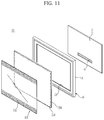
- FIG. 11 is a perspective view illustrating a configuration of a display device in accordance with another embodiment of the present disclosure.
- a film 10 d is provided with a black matrix 12 d formed thereto.
- the black matrix 12 d is only formed at an upper side peripheral and a lower side peripheral of the four peripherals.
- the display panel 20 d and a pattern 22 d may only be formed at an upper side and a lower side of the display panel 20 d .
- the black matrix 12 d which is configured to cover such, is also formed only at the upper side and the lower side of the display panel 20 d.
- the pattern 22 d is formed only at one side peripheral of the display panel 20 d
- the black matrix 12 d also is formed only at one side peripheral of the display panel 20 d.
- FIG. 12 is a perspective view, illustrating a configuration of a display device, in accordance with another embodiment of the present disclosure.
- black matrixes 12 e and 12 f are formed such that the entire four peripherals of a display panel 20 e may be covered.
- the black matrixes 12 f positioned at a left peripheral and a right peripheral, are formed on the display panel 20 e .
- the black matrixes 12 e positioned at an upper peripheral and a lower peripheral are formed on a film 10 e.
- the black matrixes 12 e and 12 f may be able to cover the entire patterns formed at the four peripherals of the display panel 20 e.
- the black matrixes being positioned at the left side peripheral and the right side peripheral, are formed on the film 10 e
- the black matrixes being positioned at the upper side peripheral and the lower side peripheral, are formed on the display panel 20 e.
- FIGS. 13 to 16 are drawings illustrating a structure of a display device in accordance with another embodiment of the present disclosure.
- the display device is illustrated on FIG. 13 , while a film is omitted.
- a display device 100 includes a display panel 110 and a side cover 120 , disposed to form a side surface exterior of the display device 100 .
- the display panel 110 is provided with an active area 112 , composed to display an image, and an inactive area 114 , being positioned at an outer portion of the active area 112 and at which an image is not being displayed.
- the inactive area 114 is provided with a pattern 115 , formed to authorize an electrical signal to the active area 112 .
- the display panel 110 may be directly supported by being attached to the support unit 124 , or may be supported at the support unit 124 by using at least one structure as a medium.
- a front of the inactive area 114 of the display panel 110 is provided with a black matrix 130 to cover the pattern 115 of the inactive area 114 .
- a front of the display panel 110 is provided with a disposed film 140
- a front of the film 140 is provided with the black matrix 130 formed.
- the black matrix 130 may be formed in between a front surface of the film 140 and a front surface of the display panel 110 .
- the black matrix 130 may be formed at a front of the display panel 110 .
- a rear of the support unit 124 , of the side cover 120 may be provided with a rear cover 150 to form a rear surface exterior of the display device 100 , and a middle panel 160 , may be provided in between the display panel 110 and the rear cover 150 , to reinforce the display panel 110 .
- the middle panel 160 in order to prevent the display panel 110 from being deformed or damaged, may be attached to the display panel 110 .
- the middle panel 160 may be attached to a rear surface of the display panel 110 by use of an adhesive member 172 .
- the adhesive member 172 may be composed with a double-sided tape.
- the middle panel 160 may be composed to be light weight. In addition to reinforcing the display panel 110 , the middle panel 160 may help the display panel 110 radiating heat.
- the middle panel 160 may include a spacer, interpositioned in between the two sheets, and the two sheets are disposed while being spaced apart in a predetermined distance from each other.
- the spacer may be composed with a plastic plate having a honeycomb structure or a plastic plate, having a crease structure in a shape of waves.
- the middle panel 160 may be provided with metallic material to effectively perform heat radiation.
- a rear of the middle panel 160 may be provided with at least one disposed printed circuit board.
- the printed circuit board is accommodated at a space in between the middle panel 160 and the rear cover 150 .
- At least one printed circuit board may include a main board 162 , to supply an image signal to the display panel 110 , and a power supply board 164 , to supply power to the display panel 110 .
- a rear of the middle panel 160 is provided with a coupled holder 166 , and the main board 162 and the power supply board 164 may be mounted at the holder 166 .
- a bracket panel 180 may be provided in between the display panel 110 and the rear cover 150 .
- the bracket panel 180 may be provided with aluminum material having a light weight and high durability.
- the bracket panel 180 includes a first panel coupling unit 182 attached to the display panel 110 , and a second panel coupling unit 184 attached to the middle panel 160 .
- the first panel coupling unit 182 is attached from an outer side of the side surface of the middle panel 160 , to reinforce the strength of the peripheral of the display panel 110 .
- the second panel coupling unit 184 is disposed in between the middle panel 160 and the rear cover 150 , to be attached to a rear surface of the middle panel 160 .
- the bracket panel 180 by use of an adhesive member 174 , may be attached to the display panel 110 and the middle panel 160 .
- the adhesive member 174 may be composed with a double-sided tape.
- a portion 182 a of the first panel coupling unit 182 is disposed in between the display panel 110 and the support unit 124 of the side cover 120 , and may be coupled to the support unit 124 .
- the support unit 124 of the side cover 120 is provided with a coupling bump 125 , protruded toward a front.
- a coupling groove 183 may be provided at the first panel coupling unit 182 , such that the coupling bump 125 of the support unit 125 may be inserted into the coupling groove 183 .
- the portion 182 a of the first panel coupling unit 182 and the support unit 124 of the side cover 120 may be coupled to each other by use of a coupling member, such as a screw.
- a rear of the display panel 110 is provided with a printed circuit board 190 , to drive the display panel 110 .
- the printed circuit board 190 is electrically connected to the display panel 110 through a connecting film 192 .
- the printed circuit board 190 may be connected to the main board 162 and the power supply board 164 through a cable (not shown).
- a space is formed in between the other portion 182 b of the first panel coupling unit 182 at the bracket panel 180 and the rear cover 150 .
- the printed circuit board 190 is accommodated at the space 102 .
- the peripheral unit 34 may comprise a peripheral frame
- the support unit 31 may comprise a support frame
- the first panel coupling unit 182 may comprise a first panel coupling portion
- the second panel coupling unit 184 may comprise a second panel coupling portion.
- the peripheral unit 34 , the support unit 31 , the first panel coupling unit 182 , and the second panel coupling unit 184 may comprise any hardware that would be within the knowledge of those skilled in the art.
Landscapes
- Physics & Mathematics (AREA)
- Nonlinear Science (AREA)
- General Physics & Mathematics (AREA)
- Optics & Photonics (AREA)
- Crystallography & Structural Chemistry (AREA)
- Chemical & Material Sciences (AREA)
- Mathematical Physics (AREA)
- Engineering & Computer Science (AREA)
- Theoretical Computer Science (AREA)
- Computer Hardware Design (AREA)
- General Engineering & Computer Science (AREA)
- Human Computer Interaction (AREA)
- Devices For Indicating Variable Information By Combining Individual Elements (AREA)
- Electroluminescent Light Sources (AREA)
Abstract
Description
Claims (7)
Priority Applications (2)
| Application Number | Priority Date | Filing Date | Title |
|---|---|---|---|
| US16/167,778 US10678080B2 (en) | 2011-12-30 | 2018-10-23 | Display device |
| US16/260,438 US10678082B2 (en) | 2011-12-30 | 2019-01-29 | Display device |
Applications Claiming Priority (4)
| Application Number | Priority Date | Filing Date | Title |
|---|---|---|---|
| KR10-2011-0147720 | 2011-12-30 | ||
| KR1020110147720A KR101945948B1 (en) | 2011-12-30 | 2011-12-30 | Display device |
| US13/728,452 US10151938B2 (en) | 2011-12-30 | 2012-12-27 | Display device |
| US16/167,778 US10678080B2 (en) | 2011-12-30 | 2018-10-23 | Display device |
Related Parent Applications (1)
| Application Number | Title | Priority Date | Filing Date |
|---|---|---|---|
| US13/728,452 Continuation US10151938B2 (en) | 2011-12-30 | 2012-12-27 | Display device |
Related Child Applications (1)
| Application Number | Title | Priority Date | Filing Date |
|---|---|---|---|
| US16/260,438 Continuation US10678082B2 (en) | 2011-12-30 | 2019-01-29 | Display device |
Publications (2)
| Publication Number | Publication Date |
|---|---|
| US20190056606A1 US20190056606A1 (en) | 2019-02-21 |
| US10678080B2 true US10678080B2 (en) | 2020-06-09 |
Family
ID=48694632
Family Applications (3)
| Application Number | Title | Priority Date | Filing Date |
|---|---|---|---|
| US13/728,452 Active 2034-02-09 US10151938B2 (en) | 2011-12-30 | 2012-12-27 | Display device |
| US16/167,778 Active US10678080B2 (en) | 2011-12-30 | 2018-10-23 | Display device |
| US16/260,438 Active US10678082B2 (en) | 2011-12-30 | 2019-01-29 | Display device |
Family Applications Before (1)
| Application Number | Title | Priority Date | Filing Date |
|---|---|---|---|
| US13/728,452 Active 2034-02-09 US10151938B2 (en) | 2011-12-30 | 2012-12-27 | Display device |
Family Applications After (1)
| Application Number | Title | Priority Date | Filing Date |
|---|---|---|---|
| US16/260,438 Active US10678082B2 (en) | 2011-12-30 | 2019-01-29 | Display device |
Country Status (2)
| Country | Link |
|---|---|
| US (3) | US10151938B2 (en) |
| KR (1) | KR101945948B1 (en) |
Families Citing this family (21)
| Publication number | Priority date | Publication date | Assignee | Title |
|---|---|---|---|---|
| KR20140067500A (en) * | 2012-11-26 | 2014-06-05 | 삼성디스플레이 주식회사 | Flat display device |
| US9543366B2 (en) * | 2013-05-15 | 2017-01-10 | Boe Technology Group Co., Ltd. | Display panel and display apparatus having the same |
| KR102040612B1 (en) * | 2013-08-21 | 2019-11-05 | 엘지전자 주식회사 | Display device |
| CN103489379B (en) * | 2013-09-27 | 2016-04-13 | 京东方科技集团股份有限公司 | Display device |
| CN105575993B (en) * | 2014-10-15 | 2018-07-24 | 上海和辉光电有限公司 | Organic light-emitting display device and preparation method thereof |
| KR20160085202A (en) * | 2015-01-07 | 2016-07-15 | 삼성전자주식회사 | Display apparatus |
| EP3182194B1 (en) | 2015-12-17 | 2019-06-19 | Lg Electronics Inc. | Display device |
| KR102455465B1 (en) * | 2015-12-17 | 2022-10-17 | 엘지전자 주식회사 | Display device |
| US10231346B2 (en) * | 2016-05-27 | 2019-03-12 | Lg Electronics Inc. | Display device |
| EP3249452B1 (en) * | 2016-05-27 | 2021-03-03 | LG Electronics Inc. | Display device |
| KR102715641B1 (en) * | 2016-05-27 | 2024-10-11 | 엘지전자 주식회사 | Display device |
| KR102644261B1 (en) * | 2016-08-08 | 2024-03-07 | 엘지전자 주식회사 | Display device |
| CN106097911B (en) * | 2016-08-04 | 2019-11-01 | 京东方科技集团股份有限公司 | Display module, the display equipment with display module, and preparation method thereof |
| US10459266B2 (en) | 2016-08-04 | 2019-10-29 | Boe Technology Group Co., Ltd. | Display module, display apparatus having the same, and fabricating method thereof |
| US10838452B2 (en) * | 2018-02-07 | 2020-11-17 | Microsoft Technology Licensing, Llc | Computing device display bonding |
| KR102551690B1 (en) * | 2018-12-06 | 2023-07-05 | 삼성전자주식회사 | Electronic device with bonding structure |
| KR102612785B1 (en) * | 2018-12-20 | 2023-12-13 | 엘지전자 주식회사 | Display device |
| KR20200133096A (en) * | 2019-05-16 | 2020-11-26 | 희성전자 주식회사 | Display device and method of joining middle cabinet and back cover of display device |
| KR102782041B1 (en) * | 2020-01-06 | 2025-03-13 | 엘지전자 주식회사 | Display device |
| KR20210090779A (en) | 2020-01-10 | 2021-07-21 | 삼성디스플레이 주식회사 | Display apparatus and manufacturing the same |
| KR102480970B1 (en) * | 2022-06-22 | 2022-12-26 | 주식회사 한성시스코 | Home automation controller with temperature compensation |
Citations (110)
| Publication number | Priority date | Publication date | Assignee | Title |
|---|---|---|---|---|
| US5666177A (en) | 1996-02-26 | 1997-09-09 | Industrial Technology Research Institute | Black matrix for liquid crystal display |
| US5666261A (en) | 1995-09-25 | 1997-09-09 | At&T Global Information Solutions Company | Honeycomb celled-sheet layer composite panel for monitoring an LCD to a laptop computer |
| US6072556A (en) | 1997-10-06 | 2000-06-06 | Semiconductor Energy Laboratory Co., Ltd. | Liquid crystal display with an adjustment layer to even out height difference in the sealant region |
| US6342932B1 (en) | 1998-11-12 | 2002-01-29 | Matshushita Electric Industrial Co., Ltd. | Liquid crystal display |
| US6532152B1 (en) | 1998-11-16 | 2003-03-11 | Intermec Ip Corp. | Ruggedized hand held computer |
| US6560124B1 (en) | 1998-10-30 | 2003-05-06 | Matsushita Electric Industrial Co., Ltd. | Display device with plasma display panel |
| US6611302B1 (en) | 1999-07-14 | 2003-08-26 | Nec Lcd Technologies, Ltd. | Flat panel display device |
| US20040246397A1 (en) | 2003-03-10 | 2004-12-09 | Sung-Yong Kang | Backlight assembly, liquid crystal display apparatus having the same and device for forming a particle interceptor in the backlight assembly |
| US6853409B2 (en) | 1999-12-22 | 2005-02-08 | Yutaka Takeishi | Signal processing circuit board and liquid crystal display apparatus with variable resistor which are hardly declined in the mechanical strength while its variable resistor is not limited to one particular location for the installation |
| US20050135724A1 (en) * | 2003-12-19 | 2005-06-23 | Henry Helvajian | Integrated glass ceramic systems |
| US20050286228A1 (en) * | 2004-06-24 | 2005-12-29 | Ki-Jung Kim | Plasma display panel assembly |
| US20060098152A1 (en) | 2004-11-05 | 2006-05-11 | Park Doo-Soon | Display apparatus |
| US20060104023A1 (en) | 2004-11-17 | 2006-05-18 | Kyung-Kyun Lee | Display apparatus |
| KR20060059429A (en) | 2004-11-29 | 2006-06-02 | 삼성전자주식회사 | Display panel protective film for display devices |
| US20060132946A1 (en) * | 2004-12-17 | 2006-06-22 | Sok-San Kim | Plasma display panel (PDP) assembly |
| KR20060079694A (en) | 2005-01-03 | 2006-07-06 | 삼성전자주식회사 | Flexible printed circuit board protective film member and flat display device using same |
| US20070079537A1 (en) | 2005-09-26 | 2007-04-12 | Kyoung-Don Lee | Display device |
| US20070229731A1 (en) | 2006-03-08 | 2007-10-04 | Chi Mei Optoelectronics Corp. | Direct type backlight module and application thereof |
| JP3991656B2 (en) | 2001-11-09 | 2007-10-17 | セイコーエプソン株式会社 | Liquid crystal panel module and projection device using the same |
| US7310222B2 (en) | 1997-03-21 | 2007-12-18 | Chunghwa Picture Tubes, Ltd. | Flat-panel display mounting system for portable computer |
| US20080035811A1 (en) | 2006-08-14 | 2008-02-14 | Samsung Electronics Co., Ltd. | Apparatus for supporting display device |
| US20080055834A1 (en) | 2006-09-01 | 2008-03-06 | Yukio Matsuzaki | Display Device |
| US20080225204A1 (en) * | 2007-01-12 | 2008-09-18 | Yasuyuki Mishima | Liquid crystal display module |
| US20080291383A1 (en) | 2007-05-25 | 2008-11-27 | Innolux Display Corp. | Liquid crystal panel with protrusions for narrowing gap between substrates thereof and method for manufacuring same |
| US20080297999A1 (en) | 2007-06-04 | 2008-12-04 | Choi Man Yong | Display apparatus |
| US20090002623A1 (en) | 2007-03-27 | 2009-01-01 | Epson Imaging Devices Corporation | Electro-optic device |
| US20090009680A1 (en) | 2007-02-08 | 2009-01-08 | Funai Electric Co., Ltd. | Liquid crystal display device |
| US20090073675A1 (en) | 2005-05-20 | 2009-03-19 | Sharp Kabushiki Kaisha | Chassis for an illuminating unit, and an illuminating unit, a display device and a television receiver incorporating the chassis |
| US20090079904A1 (en) | 2007-09-25 | 2009-03-26 | Fujitsu Limited | Liquid crystal display device |
| US20090115931A1 (en) | 2007-11-06 | 2009-05-07 | Lg Display Co., Ltd. | Backlight unit and liquid crystal dispaly module including the same |
| US20090115928A1 (en) | 2007-11-06 | 2009-05-07 | Shin Chung-Hyuk | Liquid crystal display device having printed circut board and method for assembling the printed circuit board |
| US20090168319A1 (en) | 2007-12-28 | 2009-07-02 | Samsung Electronics Co. Ltd. | Display, front cover thereof, mold of front cover, and manufacturing method for front cover |
| US20090167171A1 (en) | 2007-11-22 | 2009-07-02 | Samsung Mobile Display Co., Ltd. | Display device, organic light emitting diode display and manufacturing method of the same |
| US20090180049A1 (en) | 2007-11-15 | 2009-07-16 | Sang-Rae Lee | Coupling means and display device using the same |
| US20090185341A1 (en) * | 2008-01-19 | 2009-07-23 | Samsung Electronics Co., Ltd. | Panel type display device |
| US20090207327A1 (en) | 2008-02-15 | 2009-08-20 | Seiko Epson Corporation | Liquid crystal apparatus, projection apparatus and electronic equipment |
| US20090207102A1 (en) | 2008-02-20 | 2009-08-20 | Ik Chang Choi | Liquid crystal display module |
| US20090207334A1 (en) | 2008-02-15 | 2009-08-20 | Kim Minseop | Backlight unit and liquid crystal display using the same |
| US20090213292A1 (en) | 2008-02-21 | 2009-08-27 | Hong-Sik Park | Flat panel display device |
| US20090231506A1 (en) | 2005-03-15 | 2009-09-17 | Sharp Kabushiki Kaisha | Display device and a televsion receiver having the same |
| US20090231509A1 (en) | 2008-03-12 | 2009-09-17 | Hong Fu Jin Precision Industry (Shenzhen) Co., Ltd. | Liquid crystal display module and method for assembling the same |
| US20090262275A1 (en) | 2008-04-21 | 2009-10-22 | Lg Display Co., Ltd. | Liquid crystal display device |
| US20090262554A1 (en) | 2008-04-17 | 2009-10-22 | Samsung Electronics Co., Ltd. | Display apparatus |
| US20090290327A1 (en) | 2008-05-21 | 2009-11-26 | Kim Heung-Seok | Backlight assembly and display device having the same |
| US20090289880A1 (en) | 2008-05-21 | 2009-11-26 | Samsung Electronics Co., Ltd | Display device and bottom chassis thereof |
| US20100038117A1 (en) | 2008-08-18 | 2010-02-18 | Chung Yechung | Tape wiring substrates and packages including the same |
| US20100053912A1 (en) | 2008-08-29 | 2010-03-04 | Kabushiki Kaisha Toshiba | Display apparatus |
| US20100060601A1 (en) | 2008-09-05 | 2010-03-11 | Hitachi Displays, Ltd. | Liquid crystal display device |
| US20100073582A1 (en) | 2008-09-19 | 2010-03-25 | Hitachi Consumer Electronics, Co., Ltd. | Liquid crystal display device and video display device using the same |
| US20100079942A1 (en) | 2008-09-26 | 2010-04-01 | Taku Yamamoto | Video display apparatus |
| US20100118250A1 (en) | 2007-03-30 | 2010-05-13 | Sharp Kabushiki Kaisha | Liquid crystal display device |
| US20100123864A1 (en) | 2008-11-18 | 2010-05-20 | Hitachi Displays, Ltd. | Liquid crystal display device |
| US20100141567A1 (en) * | 2008-12-05 | 2010-06-10 | Au Optronics Corporation | Display Device and Manufacture Method Thereof |
| US20100165235A1 (en) | 2008-12-30 | 2010-07-01 | Lee Young-Bin | Liquid crystal display device |
| US20100165253A1 (en) | 2008-12-29 | 2010-07-01 | Samsung Electronics Co. Ltd | Backlight assembly and liquid crystal display having the same |
| US20100165233A1 (en) | 2008-12-29 | 2010-07-01 | Samsung Electronics Co., Ltd | Backlight unit and liquid crystal display having the same |
| US20100165237A1 (en) | 2008-12-30 | 2010-07-01 | Samsung Electronics Co., Ltd. | Backlight unit and liquid crystal display having the same |
| US20100165244A1 (en) | 2008-12-26 | 2010-07-01 | Jin-Soo Shin | Liquid crystal display and fabricating method thereof |
| US20100171897A1 (en) | 2009-01-06 | 2010-07-08 | Samsung Electronics Co. Ltd. | Liquid crystal display device |
| US20100177259A1 (en) | 2006-08-11 | 2010-07-15 | Sharp Kabushiki Kaisha | Display apparatus and electronic apparatus with the same |
| US20100188607A1 (en) | 2009-01-29 | 2010-07-29 | Samsung Electronics Co., Ltd. | Backlight assembly and display device including the same |
| US20100188596A1 (en) | 2009-01-23 | 2010-07-29 | Coretronic Display Solution Corporation | Display |
| US20100238365A1 (en) | 2007-10-30 | 2010-09-23 | Sharp Kabushiki Kaisha | Information display |
| KR20100105260A (en) | 2009-03-20 | 2010-09-29 | 엘지전자 주식회사 | Display apparatus |
| US20100253874A1 (en) | 2007-10-29 | 2010-10-07 | Keita Ito | Display device |
| US20100259881A1 (en) | 2009-04-09 | 2010-10-14 | Samsung Electronics Co., Ltd | Display apparatus |
| US20100259488A1 (en) | 2009-04-13 | 2010-10-14 | Microsoft Corporation | Avoiding optical effects of touch on liquid crystal display |
| US20100265430A1 (en) * | 2009-04-17 | 2010-10-21 | Innocom Technology (Shenzhen) Co., Ltd. | Display device with conductive masking film for discharging static electricity |
| US20100271568A1 (en) | 2009-04-27 | 2010-10-28 | Samsung Electronics Co., Ltd. | Backlight assembly and liquid crystal display |
| US20100283935A1 (en) | 2009-05-08 | 2010-11-11 | Jae-Sung Park | Liquid crystal device and method of fabricating liquid crystal display device module including the same |
| US20100309102A1 (en) | 2009-06-08 | 2010-12-09 | Samsung Electronics Co., Ltd. | Display apparatus and control method thereof |
| US20100309406A1 (en) | 2009-06-09 | 2010-12-09 | Min Joo Kim | Backlight unit and liquid crystal display device having the same |
| US20100315570A1 (en) | 2009-06-11 | 2010-12-16 | Mathew Dinesh C | Portable computer display structures |
| US20100328568A1 (en) * | 2009-06-24 | 2010-12-30 | Lee Kyuheon | Liquid crystal display |
| US20100328862A1 (en) * | 2009-06-26 | 2010-12-30 | Chung-Min Wang | Display device |
| US20100328573A1 (en) | 2009-06-24 | 2010-12-30 | Lg Display Co., Ltd. | Liquid crystal display device |
| US20110002112A1 (en) | 2009-07-02 | 2011-01-06 | Au Optronics Corporation | Display Device with Panel Positioning Structure and Method for Manufacturing the Same |
| US20110018462A1 (en) | 2009-07-27 | 2011-01-27 | VIZIO Inc. | System, method and apparatus for illuminating a bezel |
| US20110051348A1 (en) | 2009-08-25 | 2011-03-03 | Samsung Electronics Co., Ltd. | Display apparatus and portable computer having the same |
| US20110069055A1 (en) * | 2009-09-22 | 2011-03-24 | Samsung Electronics Co., Ltd | Display apparatus |
| KR20110032110A (en) | 2009-09-22 | 2011-03-30 | 엘지디스플레이 주식회사 | Display device |
| US20110096569A1 (en) | 2008-07-10 | 2011-04-28 | Sharp Kabushiki Kaisha | Backlight device and flat display device using same |
| US20110102701A1 (en) | 2009-10-30 | 2011-05-05 | Chimei Innolux Corporation | Liquid crystal display device |
| US20110110046A1 (en) | 2008-07-15 | 2011-05-12 | Sharp Kabushiki Kaisha | Reinforcement frame, component unit, and display |
| US20110116218A1 (en) | 2009-11-18 | 2011-05-19 | Samsung Electronics Co., Ltd. | Display apparatus |
| US20110122334A1 (en) | 2009-11-20 | 2011-05-26 | Chimei Innolux Corporation | Liquid crystal display, method for assembling same, and display apparatus |
| US20110134346A1 (en) | 2008-08-22 | 2011-06-09 | Sharp Kabushiki Kaisha | Display device and television receiver |
| KR20110064433A (en) | 2009-12-08 | 2011-06-15 | 엘지전자 주식회사 | Back light unit and display device including same |
| US20110148869A1 (en) | 2009-12-21 | 2011-06-23 | Samsung Electronics Co., Ltd. | Display apparatus |
| US20110149198A1 (en) | 2009-12-23 | 2011-06-23 | Youngmin Kim | Display device |
| US20110157511A1 (en) | 2009-12-24 | 2011-06-30 | Cheng-Hung Hsu | Display device |
| US20110205454A1 (en) | 2008-12-29 | 2011-08-25 | Yun-Joo Kim | Display apparatus |
| US20110216485A1 (en) | 2010-03-05 | 2011-09-08 | Laio Kang | Module for expanding function of mobile device and mobile device having the same |
| US20110221677A1 (en) | 2008-03-20 | 2011-09-15 | Acco Brands Usa Llc | 3-Axis Trackball |
| KR20110103729A (en) | 2010-03-15 | 2011-09-21 | 엘지전자 주식회사 | Display device |
| US20110227848A1 (en) | 2010-03-16 | 2011-09-22 | Hitachi Displays, Ltd. | Display device |
| US20110234937A1 (en) | 2010-03-24 | 2011-09-29 | Samsung Mobile Display Co., Ltd. | Mold frame and liquid crystal display device using the same |
| US20110242438A1 (en) | 2008-12-19 | 2011-10-06 | Sharp Kabushiki Kaisha | Lighting unit, display device, and television receiver |
| US20110261282A1 (en) | 2010-04-27 | 2011-10-27 | Ki Nam Jean | Display device |
| US20110267751A1 (en) | 2009-01-23 | 2011-11-03 | Sharp Kabushiki Kaisha | Display device and frame mountable on the display device |
| US20110267556A1 (en) | 2009-01-15 | 2011-11-03 | Sharp Kabushiki Kaisha | Liquid crystal display device and board clip mountable on the liquid crystal display device |
| US20110273641A1 (en) | 2009-01-14 | 2011-11-10 | Sharp Kabushiki Kaisha | Liquid crystal display device and frame for liquid crystal display device |
| US20110273631A1 (en) | 2009-01-13 | 2011-11-10 | Sharp Kabushiki Kaisha | Lighting device, display device and television receiver |
| US20110298751A1 (en) | 2010-06-07 | 2011-12-08 | David Merel | Multi-User Interactive Coffee Table |
| US20120050639A1 (en) | 2011-01-12 | 2012-03-01 | Kim Cheolsoo | Display apparatus |
| US20120052214A1 (en) | 2010-09-01 | 2012-03-01 | Industrial Technology Research Institute | Method for patterning flexible substrate |
| US20120224343A1 (en) | 2011-03-02 | 2012-09-06 | Seiko Epson Corporation | Electrical device |
| US20120327328A1 (en) * | 2011-06-24 | 2012-12-27 | Lg Display Co., Ltd. | Liquid crystal display device |
| US20130170116A1 (en) * | 2011-12-30 | 2013-07-04 | Samsung Electronics Co., Ltd. | Display device |
| US8575735B2 (en) | 2010-02-26 | 2013-11-05 | Samsung Electronics Co., Ltd. | Semiconductor chip and film and TAB package comprising the chip and film |
Family Cites Families (1)
| Publication number | Priority date | Publication date | Assignee | Title |
|---|---|---|---|---|
| TWI389067B (en) * | 2010-06-29 | 2013-03-11 | Compal Electronics Inc | Display module and assembly method thereof |
-
2011
- 2011-12-30 KR KR1020110147720A patent/KR101945948B1/en active Active
-
2012
- 2012-12-27 US US13/728,452 patent/US10151938B2/en active Active
-
2018
- 2018-10-23 US US16/167,778 patent/US10678080B2/en active Active
-
2019
- 2019-01-29 US US16/260,438 patent/US10678082B2/en active Active
Patent Citations (111)
| Publication number | Priority date | Publication date | Assignee | Title |
|---|---|---|---|---|
| US5666261A (en) | 1995-09-25 | 1997-09-09 | At&T Global Information Solutions Company | Honeycomb celled-sheet layer composite panel for monitoring an LCD to a laptop computer |
| US5666177A (en) | 1996-02-26 | 1997-09-09 | Industrial Technology Research Institute | Black matrix for liquid crystal display |
| US7310222B2 (en) | 1997-03-21 | 2007-12-18 | Chunghwa Picture Tubes, Ltd. | Flat-panel display mounting system for portable computer |
| US6072556A (en) | 1997-10-06 | 2000-06-06 | Semiconductor Energy Laboratory Co., Ltd. | Liquid crystal display with an adjustment layer to even out height difference in the sealant region |
| US6560124B1 (en) | 1998-10-30 | 2003-05-06 | Matsushita Electric Industrial Co., Ltd. | Display device with plasma display panel |
| US6342932B1 (en) | 1998-11-12 | 2002-01-29 | Matshushita Electric Industrial Co., Ltd. | Liquid crystal display |
| US6532152B1 (en) | 1998-11-16 | 2003-03-11 | Intermec Ip Corp. | Ruggedized hand held computer |
| US6611302B1 (en) | 1999-07-14 | 2003-08-26 | Nec Lcd Technologies, Ltd. | Flat panel display device |
| US6853409B2 (en) | 1999-12-22 | 2005-02-08 | Yutaka Takeishi | Signal processing circuit board and liquid crystal display apparatus with variable resistor which are hardly declined in the mechanical strength while its variable resistor is not limited to one particular location for the installation |
| JP3991656B2 (en) | 2001-11-09 | 2007-10-17 | セイコーエプソン株式会社 | Liquid crystal panel module and projection device using the same |
| US20040246397A1 (en) | 2003-03-10 | 2004-12-09 | Sung-Yong Kang | Backlight assembly, liquid crystal display apparatus having the same and device for forming a particle interceptor in the backlight assembly |
| US20050135724A1 (en) * | 2003-12-19 | 2005-06-23 | Henry Helvajian | Integrated glass ceramic systems |
| US20050286228A1 (en) * | 2004-06-24 | 2005-12-29 | Ki-Jung Kim | Plasma display panel assembly |
| US20060098152A1 (en) | 2004-11-05 | 2006-05-11 | Park Doo-Soon | Display apparatus |
| US20060104023A1 (en) | 2004-11-17 | 2006-05-18 | Kyung-Kyun Lee | Display apparatus |
| KR20060059429A (en) | 2004-11-29 | 2006-06-02 | 삼성전자주식회사 | Display panel protective film for display devices |
| US20060132946A1 (en) * | 2004-12-17 | 2006-06-22 | Sok-San Kim | Plasma display panel (PDP) assembly |
| KR20060079694A (en) | 2005-01-03 | 2006-07-06 | 삼성전자주식회사 | Flexible printed circuit board protective film member and flat display device using same |
| US20090231506A1 (en) | 2005-03-15 | 2009-09-17 | Sharp Kabushiki Kaisha | Display device and a televsion receiver having the same |
| US20090073675A1 (en) | 2005-05-20 | 2009-03-19 | Sharp Kabushiki Kaisha | Chassis for an illuminating unit, and an illuminating unit, a display device and a television receiver incorporating the chassis |
| US20070079537A1 (en) | 2005-09-26 | 2007-04-12 | Kyoung-Don Lee | Display device |
| US20070229731A1 (en) | 2006-03-08 | 2007-10-04 | Chi Mei Optoelectronics Corp. | Direct type backlight module and application thereof |
| US20100177259A1 (en) | 2006-08-11 | 2010-07-15 | Sharp Kabushiki Kaisha | Display apparatus and electronic apparatus with the same |
| US20080035811A1 (en) | 2006-08-14 | 2008-02-14 | Samsung Electronics Co., Ltd. | Apparatus for supporting display device |
| US20080055834A1 (en) | 2006-09-01 | 2008-03-06 | Yukio Matsuzaki | Display Device |
| US20080225204A1 (en) * | 2007-01-12 | 2008-09-18 | Yasuyuki Mishima | Liquid crystal display module |
| US20090009680A1 (en) | 2007-02-08 | 2009-01-08 | Funai Electric Co., Ltd. | Liquid crystal display device |
| US20090002623A1 (en) | 2007-03-27 | 2009-01-01 | Epson Imaging Devices Corporation | Electro-optic device |
| US20100118250A1 (en) | 2007-03-30 | 2010-05-13 | Sharp Kabushiki Kaisha | Liquid crystal display device |
| US20080291383A1 (en) | 2007-05-25 | 2008-11-27 | Innolux Display Corp. | Liquid crystal panel with protrusions for narrowing gap between substrates thereof and method for manufacuring same |
| US20080297999A1 (en) | 2007-06-04 | 2008-12-04 | Choi Man Yong | Display apparatus |
| US20090079904A1 (en) | 2007-09-25 | 2009-03-26 | Fujitsu Limited | Liquid crystal display device |
| US20100253874A1 (en) | 2007-10-29 | 2010-10-07 | Keita Ito | Display device |
| US20100238365A1 (en) | 2007-10-30 | 2010-09-23 | Sharp Kabushiki Kaisha | Information display |
| US20090115928A1 (en) | 2007-11-06 | 2009-05-07 | Shin Chung-Hyuk | Liquid crystal display device having printed circut board and method for assembling the printed circuit board |
| US20090115931A1 (en) | 2007-11-06 | 2009-05-07 | Lg Display Co., Ltd. | Backlight unit and liquid crystal dispaly module including the same |
| US20090180049A1 (en) | 2007-11-15 | 2009-07-16 | Sang-Rae Lee | Coupling means and display device using the same |
| US20090167171A1 (en) | 2007-11-22 | 2009-07-02 | Samsung Mobile Display Co., Ltd. | Display device, organic light emitting diode display and manufacturing method of the same |
| US20090168319A1 (en) | 2007-12-28 | 2009-07-02 | Samsung Electronics Co. Ltd. | Display, front cover thereof, mold of front cover, and manufacturing method for front cover |
| US20090185341A1 (en) * | 2008-01-19 | 2009-07-23 | Samsung Electronics Co., Ltd. | Panel type display device |
| US20090207327A1 (en) | 2008-02-15 | 2009-08-20 | Seiko Epson Corporation | Liquid crystal apparatus, projection apparatus and electronic equipment |
| US20090207334A1 (en) | 2008-02-15 | 2009-08-20 | Kim Minseop | Backlight unit and liquid crystal display using the same |
| US20090207102A1 (en) | 2008-02-20 | 2009-08-20 | Ik Chang Choi | Liquid crystal display module |
| US20090213292A1 (en) | 2008-02-21 | 2009-08-27 | Hong-Sik Park | Flat panel display device |
| US20090231509A1 (en) | 2008-03-12 | 2009-09-17 | Hong Fu Jin Precision Industry (Shenzhen) Co., Ltd. | Liquid crystal display module and method for assembling the same |
| US20110221677A1 (en) | 2008-03-20 | 2011-09-15 | Acco Brands Usa Llc | 3-Axis Trackball |
| US20090262554A1 (en) | 2008-04-17 | 2009-10-22 | Samsung Electronics Co., Ltd. | Display apparatus |
| US20090262275A1 (en) | 2008-04-21 | 2009-10-22 | Lg Display Co., Ltd. | Liquid crystal display device |
| US20090289880A1 (en) | 2008-05-21 | 2009-11-26 | Samsung Electronics Co., Ltd | Display device and bottom chassis thereof |
| US20090290327A1 (en) | 2008-05-21 | 2009-11-26 | Kim Heung-Seok | Backlight assembly and display device having the same |
| US20110096569A1 (en) | 2008-07-10 | 2011-04-28 | Sharp Kabushiki Kaisha | Backlight device and flat display device using same |
| US20110110046A1 (en) | 2008-07-15 | 2011-05-12 | Sharp Kabushiki Kaisha | Reinforcement frame, component unit, and display |
| US20100038117A1 (en) | 2008-08-18 | 2010-02-18 | Chung Yechung | Tape wiring substrates and packages including the same |
| US20110134346A1 (en) | 2008-08-22 | 2011-06-09 | Sharp Kabushiki Kaisha | Display device and television receiver |
| US20100053912A1 (en) | 2008-08-29 | 2010-03-04 | Kabushiki Kaisha Toshiba | Display apparatus |
| US20100060601A1 (en) | 2008-09-05 | 2010-03-11 | Hitachi Displays, Ltd. | Liquid crystal display device |
| US20100073582A1 (en) | 2008-09-19 | 2010-03-25 | Hitachi Consumer Electronics, Co., Ltd. | Liquid crystal display device and video display device using the same |
| US20100079942A1 (en) | 2008-09-26 | 2010-04-01 | Taku Yamamoto | Video display apparatus |
| US20100123864A1 (en) | 2008-11-18 | 2010-05-20 | Hitachi Displays, Ltd. | Liquid crystal display device |
| US20100141567A1 (en) * | 2008-12-05 | 2010-06-10 | Au Optronics Corporation | Display Device and Manufacture Method Thereof |
| US20110242438A1 (en) | 2008-12-19 | 2011-10-06 | Sharp Kabushiki Kaisha | Lighting unit, display device, and television receiver |
| US20100165244A1 (en) | 2008-12-26 | 2010-07-01 | Jin-Soo Shin | Liquid crystal display and fabricating method thereof |
| US20100165233A1 (en) | 2008-12-29 | 2010-07-01 | Samsung Electronics Co., Ltd | Backlight unit and liquid crystal display having the same |
| US20100165253A1 (en) | 2008-12-29 | 2010-07-01 | Samsung Electronics Co. Ltd | Backlight assembly and liquid crystal display having the same |
| US20110205454A1 (en) | 2008-12-29 | 2011-08-25 | Yun-Joo Kim | Display apparatus |
| US20100165237A1 (en) | 2008-12-30 | 2010-07-01 | Samsung Electronics Co., Ltd. | Backlight unit and liquid crystal display having the same |
| US20100165235A1 (en) | 2008-12-30 | 2010-07-01 | Lee Young-Bin | Liquid crystal display device |
| US20100171897A1 (en) | 2009-01-06 | 2010-07-08 | Samsung Electronics Co. Ltd. | Liquid crystal display device |
| US20110273631A1 (en) | 2009-01-13 | 2011-11-10 | Sharp Kabushiki Kaisha | Lighting device, display device and television receiver |
| US20110273641A1 (en) | 2009-01-14 | 2011-11-10 | Sharp Kabushiki Kaisha | Liquid crystal display device and frame for liquid crystal display device |
| US20110267556A1 (en) | 2009-01-15 | 2011-11-03 | Sharp Kabushiki Kaisha | Liquid crystal display device and board clip mountable on the liquid crystal display device |
| US20110267751A1 (en) | 2009-01-23 | 2011-11-03 | Sharp Kabushiki Kaisha | Display device and frame mountable on the display device |
| US20100188596A1 (en) | 2009-01-23 | 2010-07-29 | Coretronic Display Solution Corporation | Display |
| US20100188607A1 (en) | 2009-01-29 | 2010-07-29 | Samsung Electronics Co., Ltd. | Backlight assembly and display device including the same |
| KR20100105260A (en) | 2009-03-20 | 2010-09-29 | 엘지전자 주식회사 | Display apparatus |
| US20100259881A1 (en) | 2009-04-09 | 2010-10-14 | Samsung Electronics Co., Ltd | Display apparatus |
| US20100259488A1 (en) | 2009-04-13 | 2010-10-14 | Microsoft Corporation | Avoiding optical effects of touch on liquid crystal display |
| US20100265430A1 (en) * | 2009-04-17 | 2010-10-21 | Innocom Technology (Shenzhen) Co., Ltd. | Display device with conductive masking film for discharging static electricity |
| US20100271568A1 (en) | 2009-04-27 | 2010-10-28 | Samsung Electronics Co., Ltd. | Backlight assembly and liquid crystal display |
| US8947617B2 (en) | 2009-04-27 | 2015-02-03 | Samsung Electronics Co., Ltd. | Backlight assembly and liquid crystal display |
| US20100283935A1 (en) | 2009-05-08 | 2010-11-11 | Jae-Sung Park | Liquid crystal device and method of fabricating liquid crystal display device module including the same |
| US20100309102A1 (en) | 2009-06-08 | 2010-12-09 | Samsung Electronics Co., Ltd. | Display apparatus and control method thereof |
| US20100309406A1 (en) | 2009-06-09 | 2010-12-09 | Min Joo Kim | Backlight unit and liquid crystal display device having the same |
| US20100315570A1 (en) | 2009-06-11 | 2010-12-16 | Mathew Dinesh C | Portable computer display structures |
| US20100328573A1 (en) | 2009-06-24 | 2010-12-30 | Lg Display Co., Ltd. | Liquid crystal display device |
| US20100328568A1 (en) * | 2009-06-24 | 2010-12-30 | Lee Kyuheon | Liquid crystal display |
| US20100328862A1 (en) * | 2009-06-26 | 2010-12-30 | Chung-Min Wang | Display device |
| US20110002112A1 (en) | 2009-07-02 | 2011-01-06 | Au Optronics Corporation | Display Device with Panel Positioning Structure and Method for Manufacturing the Same |
| US20110018462A1 (en) | 2009-07-27 | 2011-01-27 | VIZIO Inc. | System, method and apparatus for illuminating a bezel |
| US20110051348A1 (en) | 2009-08-25 | 2011-03-03 | Samsung Electronics Co., Ltd. | Display apparatus and portable computer having the same |
| KR20110032110A (en) | 2009-09-22 | 2011-03-30 | 엘지디스플레이 주식회사 | Display device |
| US20110069055A1 (en) * | 2009-09-22 | 2011-03-24 | Samsung Electronics Co., Ltd | Display apparatus |
| US20110102701A1 (en) | 2009-10-30 | 2011-05-05 | Chimei Innolux Corporation | Liquid crystal display device |
| US20110116218A1 (en) | 2009-11-18 | 2011-05-19 | Samsung Electronics Co., Ltd. | Display apparatus |
| US20110122334A1 (en) | 2009-11-20 | 2011-05-26 | Chimei Innolux Corporation | Liquid crystal display, method for assembling same, and display apparatus |
| KR20110064433A (en) | 2009-12-08 | 2011-06-15 | 엘지전자 주식회사 | Back light unit and display device including same |
| US20110148869A1 (en) | 2009-12-21 | 2011-06-23 | Samsung Electronics Co., Ltd. | Display apparatus |
| US20110149198A1 (en) | 2009-12-23 | 2011-06-23 | Youngmin Kim | Display device |
| US20110157511A1 (en) | 2009-12-24 | 2011-06-30 | Cheng-Hung Hsu | Display device |
| US8575735B2 (en) | 2010-02-26 | 2013-11-05 | Samsung Electronics Co., Ltd. | Semiconductor chip and film and TAB package comprising the chip and film |
| US20110216485A1 (en) | 2010-03-05 | 2011-09-08 | Laio Kang | Module for expanding function of mobile device and mobile device having the same |
| KR20110103729A (en) | 2010-03-15 | 2011-09-21 | 엘지전자 주식회사 | Display device |
| US20110227848A1 (en) | 2010-03-16 | 2011-09-22 | Hitachi Displays, Ltd. | Display device |
| US20110234937A1 (en) | 2010-03-24 | 2011-09-29 | Samsung Mobile Display Co., Ltd. | Mold frame and liquid crystal display device using the same |
| US20110261282A1 (en) | 2010-04-27 | 2011-10-27 | Ki Nam Jean | Display device |
| US20110298751A1 (en) | 2010-06-07 | 2011-12-08 | David Merel | Multi-User Interactive Coffee Table |
| US20120052214A1 (en) | 2010-09-01 | 2012-03-01 | Industrial Technology Research Institute | Method for patterning flexible substrate |
| US20120050639A1 (en) | 2011-01-12 | 2012-03-01 | Kim Cheolsoo | Display apparatus |
| US20120224343A1 (en) | 2011-03-02 | 2012-09-06 | Seiko Epson Corporation | Electrical device |
| US20120327328A1 (en) * | 2011-06-24 | 2012-12-27 | Lg Display Co., Ltd. | Liquid crystal display device |
| US20130170116A1 (en) * | 2011-12-30 | 2013-07-04 | Samsung Electronics Co., Ltd. | Display device |
Non-Patent Citations (4)
| Title |
|---|
| Communication dated Apr. 19, 2018, issued by the Korean Intellectual Property Office in counterpart Korean Patent Application No. 10-2011-0147720. |
| Communication dated Apr. 30, 2019, issued by the Korean Intellectual Property Office in corresponding Korean Application No. 10-2019-0012029. |
| Communication dated Oct. 30, 2018, issued by the Korean Intellectual Property Office in counterpart Korean Patent Application No. 10-2011-0147720. |
| Communication dated Oct. 30, 2019 issued by the Korean Patent Office in counterpart Korean Application No. 10-2019-0012029. |
Also Published As
| Publication number | Publication date |
|---|---|
| US20190155061A1 (en) | 2019-05-23 |
| KR20130078656A (en) | 2013-07-10 |
| KR101945948B1 (en) | 2019-02-12 |
| US20130170115A1 (en) | 2013-07-04 |
| US20190056606A1 (en) | 2019-02-21 |
| US10151938B2 (en) | 2018-12-11 |
| US10678082B2 (en) | 2020-06-09 |
Similar Documents
| Publication | Publication Date | Title |
|---|---|---|
| US10678080B2 (en) | Display device | |
| US9007755B2 (en) | Flat panel type image display device and method for manufacturing the same | |
| JP4829261B2 (en) | Bonding structure of mounting frame of liquid crystal display device | |
| US9671630B2 (en) | Display device | |
| US9904082B2 (en) | Liquid crystal display device including reinforcing frame | |
| US9668363B2 (en) | Display apparatus | |
| US7777829B2 (en) | Liquid crystal display device | |
| US9888595B2 (en) | Display device | |
| KR20190069186A (en) | Back Cover and Display Device having the same | |
| KR100719658B1 (en) | Portable display | |
| US8810747B2 (en) | Liquid crystal display device | |
| KR102319801B1 (en) | Display device | |
| US9877402B2 (en) | Display device | |
| US20210068315A1 (en) | Display device | |
| KR101255279B1 (en) | Backlight Unit | |
| KR20150130210A (en) | Display apparatus | |
| US7658532B2 (en) | Portable display device | |
| KR102053640B1 (en) | Display device | |
| US10194539B2 (en) | Display device | |
| US12382591B2 (en) | Display device | |
| KR20120067075A (en) | Panel bonding method for fpd | |
| US10852575B2 (en) | Display apparatus having front cover with infrared sensor | |
| JP2007052421A (en) | Plasma display device |
Legal Events
| Date | Code | Title | Description |
|---|---|---|---|
| FEPP | Fee payment procedure |
Free format text: ENTITY STATUS SET TO UNDISCOUNTED (ORIGINAL EVENT CODE: BIG.); ENTITY STATUS OF PATENT OWNER: LARGE ENTITY |
|
| STPP | Information on status: patent application and granting procedure in general |
Free format text: DOCKETED NEW CASE - READY FOR EXAMINATION |
|
| STPP | Information on status: patent application and granting procedure in general |
Free format text: NON FINAL ACTION MAILED |
|
| STPP | Information on status: patent application and granting procedure in general |
Free format text: RESPONSE TO NON-FINAL OFFICE ACTION ENTERED AND FORWARDED TO EXAMINER |
|
| STPP | Information on status: patent application and granting procedure in general |
Free format text: NOTICE OF ALLOWANCE MAILED -- APPLICATION RECEIVED IN OFFICE OF PUBLICATIONS |
|
| STPP | Information on status: patent application and granting procedure in general |
Free format text: PUBLICATIONS -- ISSUE FEE PAYMENT VERIFIED |
|
| STCF | Information on status: patent grant |
Free format text: PATENTED CASE |
|
| MAFP | Maintenance fee payment |
Free format text: PAYMENT OF MAINTENANCE FEE, 4TH YEAR, LARGE ENTITY (ORIGINAL EVENT CODE: M1551); ENTITY STATUS OF PATENT OWNER: LARGE ENTITY Year of fee payment: 4 |