US10659000B2 - Fluidic sensor device having UV-blocking cover - Google Patents
Fluidic sensor device having UV-blocking cover Download PDFInfo
- Publication number
- US10659000B2 US10659000B2 US15/470,111 US201715470111A US10659000B2 US 10659000 B2 US10659000 B2 US 10659000B2 US 201715470111 A US201715470111 A US 201715470111A US 10659000 B2 US10659000 B2 US 10659000B2
- Authority
- US
- United States
- Prior art keywords
- cover
- fluidic
- channel
- radiation
- biomolecule
- Prior art date
- Legal status (The legal status is an assumption and is not a legal conclusion. Google has not performed a legal analysis and makes no representation as to the accuracy of the status listed.)
- Active, expires
Links
- 230000005855 radiation Effects 0.000 claims abstract description 55
- 239000000463 material Substances 0.000 claims description 92
- 239000000853 adhesive Substances 0.000 claims description 51
- 230000001070 adhesive effect Effects 0.000 claims description 48
- 238000000576 coating method Methods 0.000 claims description 40
- 239000011248 coating agent Substances 0.000 claims description 35
- 230000000903 blocking effect Effects 0.000 claims description 30
- 239000012491 analyte Substances 0.000 claims description 17
- 230000027455 binding Effects 0.000 claims description 13
- 230000005540 biological transmission Effects 0.000 claims description 12
- 150000001875 compounds Chemical class 0.000 claims description 6
- 238000004891 communication Methods 0.000 claims description 5
- 239000012634 fragment Substances 0.000 claims description 3
- 229920006332 epoxy adhesive Polymers 0.000 claims 1
- 239000010410 layer Substances 0.000 description 96
- 239000013545 self-assembled monolayer Substances 0.000 description 45
- 239000000758 substrate Substances 0.000 description 44
- 239000002094 self assembled monolayer Substances 0.000 description 37
- 238000000034 method Methods 0.000 description 32
- 239000012530 fluid Substances 0.000 description 18
- 230000009870 specific binding Effects 0.000 description 15
- 238000007306 functionalization reaction Methods 0.000 description 14
- VYPSYNLAJGMNEJ-UHFFFAOYSA-N Silicium dioxide Chemical compound O=[Si]=O VYPSYNLAJGMNEJ-UHFFFAOYSA-N 0.000 description 13
- 238000000151 deposition Methods 0.000 description 11
- 230000008569 process Effects 0.000 description 11
- 230000008021 deposition Effects 0.000 description 10
- 150000001282 organosilanes Chemical class 0.000 description 10
- 229920002120 photoresistant polymer Polymers 0.000 description 10
- 238000000682 scanning probe acoustic microscopy Methods 0.000 description 8
- 239000007788 liquid Substances 0.000 description 7
- 239000000126 substance Substances 0.000 description 7
- 150000003573 thiols Chemical class 0.000 description 7
- 239000004593 Epoxy Substances 0.000 description 6
- XLOMVQKBTHCTTD-UHFFFAOYSA-N Zinc monoxide Chemical compound [Zn]=O XLOMVQKBTHCTTD-UHFFFAOYSA-N 0.000 description 5
- 238000000231 atomic layer deposition Methods 0.000 description 5
- 230000015572 biosynthetic process Effects 0.000 description 5
- 239000013078 crystal Substances 0.000 description 5
- PCHJSUWPFVWCPO-UHFFFAOYSA-N gold Chemical compound [Au] PCHJSUWPFVWCPO-UHFFFAOYSA-N 0.000 description 5
- 229910052737 gold Inorganic materials 0.000 description 5
- 239000010931 gold Substances 0.000 description 5
- 229910000510 noble metal Inorganic materials 0.000 description 5
- 239000000377 silicon dioxide Substances 0.000 description 5
- -1 Bragg mirror Substances 0.000 description 4
- 229910052581 Si3N4 Inorganic materials 0.000 description 4
- GWEVSGVZZGPLCZ-UHFFFAOYSA-N Titan oxide Chemical compound O=[Ti]=O GWEVSGVZZGPLCZ-UHFFFAOYSA-N 0.000 description 4
- 229910052782 aluminium Inorganic materials 0.000 description 4
- XAGFODPZIPBFFR-UHFFFAOYSA-N aluminium Chemical compound [Al] XAGFODPZIPBFFR-UHFFFAOYSA-N 0.000 description 4
- 239000000872 buffer Substances 0.000 description 4
- 230000008859 change Effects 0.000 description 4
- 238000009826 distribution Methods 0.000 description 4
- 238000004519 manufacturing process Methods 0.000 description 4
- 239000000203 mixture Substances 0.000 description 4
- TWNQGVIAIRXVLR-UHFFFAOYSA-N oxo(oxoalumanyloxy)alumane Chemical compound O=[Al]O[Al]=O TWNQGVIAIRXVLR-UHFFFAOYSA-N 0.000 description 4
- 238000000206 photolithography Methods 0.000 description 4
- BASFCYQUMIYNBI-UHFFFAOYSA-N platinum Chemical compound [Pt] BASFCYQUMIYNBI-UHFFFAOYSA-N 0.000 description 4
- 102000004169 proteins and genes Human genes 0.000 description 4
- 108090000623 proteins and genes Proteins 0.000 description 4
- HQVNEWCFYHHQES-UHFFFAOYSA-N silicon nitride Chemical compound N12[Si]34N5[Si]62N3[Si]51N64 HQVNEWCFYHHQES-UHFFFAOYSA-N 0.000 description 4
- GWOLZNVIRIHJHB-UHFFFAOYSA-N 11-mercaptoundecanoic acid Chemical compound OC(=O)CCCCCCCCCCS GWOLZNVIRIHJHB-UHFFFAOYSA-N 0.000 description 3
- 229910000838 Al alloy Inorganic materials 0.000 description 3
- 229920000089 Cyclic olefin copolymer Polymers 0.000 description 3
- 239000004713 Cyclic olefin copolymer Substances 0.000 description 3
- 239000002390 adhesive tape Substances 0.000 description 3
- 230000002411 adverse Effects 0.000 description 3
- 239000000427 antigen Substances 0.000 description 3
- 230000000875 corresponding effect Effects 0.000 description 3
- 230000007797 corrosion Effects 0.000 description 3
- 238000005260 corrosion Methods 0.000 description 3
- WNAHIZMDSQCWRP-UHFFFAOYSA-N dodecane-1-thiol Chemical compound CCCCCCCCCCCCS WNAHIZMDSQCWRP-UHFFFAOYSA-N 0.000 description 3
- 239000007772 electrode material Substances 0.000 description 3
- 229910044991 metal oxide Inorganic materials 0.000 description 3
- 150000004706 metal oxides Chemical class 0.000 description 3
- 230000009871 nonspecific binding Effects 0.000 description 3
- BPUBBGLMJRNUCC-UHFFFAOYSA-N oxygen(2-);tantalum(5+) Chemical compound [O-2].[O-2].[O-2].[O-2].[O-2].[Ta+5].[Ta+5] BPUBBGLMJRNUCC-UHFFFAOYSA-N 0.000 description 3
- 239000002245 particle Substances 0.000 description 3
- 102000005962 receptors Human genes 0.000 description 3
- 108020003175 receptors Proteins 0.000 description 3
- 230000004044 response Effects 0.000 description 3
- 235000012239 silicon dioxide Nutrition 0.000 description 3
- 238000010897 surface acoustic wave method Methods 0.000 description 3
- PBCFLUZVCVVTBY-UHFFFAOYSA-N tantalum pentoxide Inorganic materials O=[Ta](=O)O[Ta](=O)=O PBCFLUZVCVVTBY-UHFFFAOYSA-N 0.000 description 3
- 239000010409 thin film Substances 0.000 description 3
- XLYOFNOQVPJJNP-UHFFFAOYSA-N water Chemical compound O XLYOFNOQVPJJNP-UHFFFAOYSA-N 0.000 description 3
- HZAXFHJVJLSVMW-UHFFFAOYSA-N 2-Aminoethan-1-ol Chemical compound NCCO HZAXFHJVJLSVMW-UHFFFAOYSA-N 0.000 description 2
- SJECZPVISLOESU-UHFFFAOYSA-N 3-trimethoxysilylpropan-1-amine Chemical compound CO[Si](OC)(OC)CCCN SJECZPVISLOESU-UHFFFAOYSA-N 0.000 description 2
- UUEWCQRISZBELL-UHFFFAOYSA-N 3-trimethoxysilylpropane-1-thiol Chemical compound CO[Si](OC)(OC)CCCS UUEWCQRISZBELL-UHFFFAOYSA-N 0.000 description 2
- PIGFYZPCRLYGLF-UHFFFAOYSA-N Aluminum nitride Chemical compound [Al]#N PIGFYZPCRLYGLF-UHFFFAOYSA-N 0.000 description 2
- 241000894006 Bacteria Species 0.000 description 2
- KDLHZDBZIXYQEI-UHFFFAOYSA-N Palladium Chemical compound [Pd] KDLHZDBZIXYQEI-UHFFFAOYSA-N 0.000 description 2
- 229920003171 Poly (ethylene oxide) Polymers 0.000 description 2
- XUIMIQQOPSSXEZ-UHFFFAOYSA-N Silicon Chemical compound [Si] XUIMIQQOPSSXEZ-UHFFFAOYSA-N 0.000 description 2
- 241000700605 Viruses Species 0.000 description 2
- 238000004458 analytical method Methods 0.000 description 2
- 102000036639 antigens Human genes 0.000 description 2
- 108091007433 antigens Proteins 0.000 description 2
- 230000008901 benefit Effects 0.000 description 2
- 125000003178 carboxy group Chemical group [H]OC(*)=O 0.000 description 2
- 238000005229 chemical vapour deposition Methods 0.000 description 2
- 230000002596 correlated effect Effects 0.000 description 2
- 238000005137 deposition process Methods 0.000 description 2
- 238000010586 diagram Methods 0.000 description 2
- 239000003989 dielectric material Substances 0.000 description 2
- 239000010408 film Substances 0.000 description 2
- IIRDTKBZINWQAW-UHFFFAOYSA-N hexaethylene glycol Chemical compound OCCOCCOCCOCCOCCOCCO IIRDTKBZINWQAW-UHFFFAOYSA-N 0.000 description 2
- 239000002648 laminated material Substances 0.000 description 2
- 239000003446 ligand Substances 0.000 description 2
- 229910052751 metal Inorganic materials 0.000 description 2
- 239000002184 metal Substances 0.000 description 2
- 125000002496 methyl group Chemical group [H]C([H])([H])* 0.000 description 2
- 238000002493 microarray Methods 0.000 description 2
- 238000012986 modification Methods 0.000 description 2
- 230000004048 modification Effects 0.000 description 2
- SLYCYWCVSGPDFR-UHFFFAOYSA-N octadecyltrimethoxysilane Chemical compound CCCCCCCCCCCCCCCCCC[Si](OC)(OC)OC SLYCYWCVSGPDFR-UHFFFAOYSA-N 0.000 description 2
- 238000004806 packaging method and process Methods 0.000 description 2
- 238000012856 packing Methods 0.000 description 2
- 238000000059 patterning Methods 0.000 description 2
- 230000002093 peripheral effect Effects 0.000 description 2
- 238000005240 physical vapour deposition Methods 0.000 description 2
- 229910052697 platinum Inorganic materials 0.000 description 2
- 230000010287 polarization Effects 0.000 description 2
- 229920001223 polyethylene glycol Polymers 0.000 description 2
- 102000040430 polynucleotide Human genes 0.000 description 2
- 108091033319 polynucleotide Proteins 0.000 description 2
- 229920001184 polypeptide Polymers 0.000 description 2
- 102000004196 processed proteins & peptides Human genes 0.000 description 2
- 108090000765 processed proteins & peptides Proteins 0.000 description 2
- 238000012545 processing Methods 0.000 description 2
- 230000001902 propagating effect Effects 0.000 description 2
- 239000004065 semiconductor Substances 0.000 description 2
- 229910052710 silicon Inorganic materials 0.000 description 2
- 239000010703 silicon Substances 0.000 description 2
- 239000007787 solid Substances 0.000 description 2
- 241000894007 species Species 0.000 description 2
- 238000004544 sputter deposition Methods 0.000 description 2
- 230000026683 transduction Effects 0.000 description 2
- 238000010361 transduction Methods 0.000 description 2
- BPSIOYPQMFLKFR-UHFFFAOYSA-N trimethoxy-[3-(oxiran-2-ylmethoxy)propyl]silane Chemical compound CO[Si](OC)(OC)CCCOCC1CO1 BPSIOYPQMFLKFR-UHFFFAOYSA-N 0.000 description 2
- 239000011787 zinc oxide Substances 0.000 description 2
- WKBPZYKAUNRMKP-UHFFFAOYSA-N 1-[2-(2,4-dichlorophenyl)pentyl]1,2,4-triazole Chemical compound C=1C=C(Cl)C=C(Cl)C=1C(CCC)CN1C=NC=N1 WKBPZYKAUNRMKP-UHFFFAOYSA-N 0.000 description 1
- 102000004506 Blood Proteins Human genes 0.000 description 1
- 108010017384 Blood Proteins Proteins 0.000 description 1
- VYZAMTAEIAYCRO-UHFFFAOYSA-N Chromium Chemical compound [Cr] VYZAMTAEIAYCRO-UHFFFAOYSA-N 0.000 description 1
- 229910000737 Duralumin Inorganic materials 0.000 description 1
- LFQSCWFLJHTTHZ-UHFFFAOYSA-N Ethanol Chemical compound CCO LFQSCWFLJHTTHZ-UHFFFAOYSA-N 0.000 description 1
- 102000014171 Milk Proteins Human genes 0.000 description 1
- 108010011756 Milk Proteins Proteins 0.000 description 1
- ZOKXTWBITQBERF-UHFFFAOYSA-N Molybdenum Chemical compound [Mo] ZOKXTWBITQBERF-UHFFFAOYSA-N 0.000 description 1
- ISWSIDIOOBJBQZ-UHFFFAOYSA-N Phenol Chemical compound OC1=CC=CC=C1 ISWSIDIOOBJBQZ-UHFFFAOYSA-N 0.000 description 1
- KJTLSVCANCCWHF-UHFFFAOYSA-N Ruthenium Chemical compound [Ru] KJTLSVCANCCWHF-UHFFFAOYSA-N 0.000 description 1
- BQCADISMDOOEFD-UHFFFAOYSA-N Silver Chemical compound [Ag] BQCADISMDOOEFD-UHFFFAOYSA-N 0.000 description 1
- NINIDFKCEFEMDL-UHFFFAOYSA-N Sulfur Chemical compound [S] NINIDFKCEFEMDL-UHFFFAOYSA-N 0.000 description 1
- 238000003848 UV Light-Curing Methods 0.000 description 1
- OBNDGIHQAIXEAO-UHFFFAOYSA-N [O].[Si] Chemical compound [O].[Si] OBNDGIHQAIXEAO-UHFFFAOYSA-N 0.000 description 1
- 239000012190 activator Substances 0.000 description 1
- 239000004840 adhesive resin Substances 0.000 description 1
- 229920006223 adhesive resin Polymers 0.000 description 1
- 125000000217 alkyl group Chemical group 0.000 description 1
- 238000013459 approach Methods 0.000 description 1
- 238000004380 ashing Methods 0.000 description 1
- 238000000277 atomic layer chemical vapour deposition Methods 0.000 description 1
- QVGXLLKOCUKJST-UHFFFAOYSA-N atomic oxygen Chemical compound [O] QVGXLLKOCUKJST-UHFFFAOYSA-N 0.000 description 1
- 230000009286 beneficial effect Effects 0.000 description 1
- RWCCWEUUXYIKHB-UHFFFAOYSA-N benzophenone Chemical compound C=1C=CC=CC=1C(=O)C1=CC=CC=C1 RWCCWEUUXYIKHB-UHFFFAOYSA-N 0.000 description 1
- 239000012965 benzophenone Substances 0.000 description 1
- 150000008366 benzophenones Chemical class 0.000 description 1
- 210000000988 bone and bone Anatomy 0.000 description 1
- 229910000420 cerium oxide Inorganic materials 0.000 description 1
- 125000003636 chemical group Chemical group 0.000 description 1
- 238000004140 cleaning Methods 0.000 description 1
- 230000006835 compression Effects 0.000 description 1
- 238000007906 compression Methods 0.000 description 1
- PMHQVHHXPFUNSP-UHFFFAOYSA-M copper(1+);methylsulfanylmethane;bromide Chemical compound Br[Cu].CSC PMHQVHHXPFUNSP-UHFFFAOYSA-M 0.000 description 1
- 230000008878 coupling Effects 0.000 description 1
- 238000010168 coupling process Methods 0.000 description 1
- 238000005859 coupling reaction Methods 0.000 description 1
- 238000005520 cutting process Methods 0.000 description 1
- 230000000254 damaging effect Effects 0.000 description 1
- 238000013016 damping Methods 0.000 description 1
- 238000011161 development Methods 0.000 description 1
- 238000006073 displacement reaction Methods 0.000 description 1
- 230000000694 effects Effects 0.000 description 1
- 125000003700 epoxy group Chemical group 0.000 description 1
- 238000005530 etching Methods 0.000 description 1
- 239000011521 glass Substances 0.000 description 1
- CJNBYAVZURUTKZ-UHFFFAOYSA-N hafnium(iv) oxide Chemical compound O=[Hf]=O CJNBYAVZURUTKZ-UHFFFAOYSA-N 0.000 description 1
- 125000002887 hydroxy group Chemical group [H]O* 0.000 description 1
- 229910010272 inorganic material Inorganic materials 0.000 description 1
- 239000011147 inorganic material Substances 0.000 description 1
- 230000003993 interaction Effects 0.000 description 1
- 229910052741 iridium Inorganic materials 0.000 description 1
- GKOZUEZYRPOHIO-UHFFFAOYSA-N iridium atom Chemical compound [Ir] GKOZUEZYRPOHIO-UHFFFAOYSA-N 0.000 description 1
- 150000002739 metals Chemical class 0.000 description 1
- 210000004080 milk Anatomy 0.000 description 1
- 239000008267 milk Substances 0.000 description 1
- 235000013336 milk Nutrition 0.000 description 1
- 229910052750 molybdenum Inorganic materials 0.000 description 1
- 239000011733 molybdenum Substances 0.000 description 1
- 238000000465 moulding Methods 0.000 description 1
- 239000002105 nanoparticle Substances 0.000 description 1
- 150000004767 nitrides Chemical class 0.000 description 1
- 125000000962 organic group Chemical group 0.000 description 1
- 229920000620 organic polymer Polymers 0.000 description 1
- 229910052762 osmium Inorganic materials 0.000 description 1
- SYQBFIAQOQZEGI-UHFFFAOYSA-N osmium atom Chemical compound [Os] SYQBFIAQOQZEGI-UHFFFAOYSA-N 0.000 description 1
- BMMGVYCKOGBVEV-UHFFFAOYSA-N oxo(oxoceriooxy)cerium Chemical compound [Ce]=O.O=[Ce]=O BMMGVYCKOGBVEV-UHFFFAOYSA-N 0.000 description 1
- 229910052760 oxygen Inorganic materials 0.000 description 1
- 239000001301 oxygen Substances 0.000 description 1
- 229910052763 palladium Inorganic materials 0.000 description 1
- 230000035515 penetration Effects 0.000 description 1
- 229920000058 polyacrylate Polymers 0.000 description 1
- 229920000647 polyepoxide Polymers 0.000 description 1
- 239000002861 polymer material Substances 0.000 description 1
- 239000011116 polymethylpentene Substances 0.000 description 1
- 229910001848 post-transition metal Inorganic materials 0.000 description 1
- 230000001737 promoting effect Effects 0.000 description 1
- 238000012552 review Methods 0.000 description 1
- 229910052703 rhodium Inorganic materials 0.000 description 1
- 239000010948 rhodium Substances 0.000 description 1
- MHOVAHRLVXNVSD-UHFFFAOYSA-N rhodium atom Chemical compound [Rh] MHOVAHRLVXNVSD-UHFFFAOYSA-N 0.000 description 1
- 229910052707 ruthenium Inorganic materials 0.000 description 1
- 230000009834 selective interaction Effects 0.000 description 1
- 150000004756 silanes Chemical class 0.000 description 1
- 125000005372 silanol group Chemical group 0.000 description 1
- 229910052814 silicon oxide Inorganic materials 0.000 description 1
- 229910052709 silver Inorganic materials 0.000 description 1
- 239000004332 silver Substances 0.000 description 1
- 239000002904 solvent Substances 0.000 description 1
- 238000005507 spraying Methods 0.000 description 1
- 229910052717 sulfur Inorganic materials 0.000 description 1
- 239000011593 sulfur Substances 0.000 description 1
- 238000012360 testing method Methods 0.000 description 1
- 239000004408 titanium dioxide Substances 0.000 description 1
- OGIDPMRJRNCKJF-UHFFFAOYSA-N titanium oxide Inorganic materials [Ti]=O OGIDPMRJRNCKJF-UHFFFAOYSA-N 0.000 description 1
- 238000012546 transfer Methods 0.000 description 1
- 230000007704 transition Effects 0.000 description 1
- 229910052723 transition metal Inorganic materials 0.000 description 1
- 238000002834 transmittance Methods 0.000 description 1
- WFKWXMTUELFFGS-UHFFFAOYSA-N tungsten Chemical compound [W] WFKWXMTUELFFGS-UHFFFAOYSA-N 0.000 description 1
- 229910052721 tungsten Inorganic materials 0.000 description 1
- 239000010937 tungsten Substances 0.000 description 1
- CCIDWXHLGNEQSL-UHFFFAOYSA-N undecane-1-thiol Chemical compound CCCCCCCCCCCS CCIDWXHLGNEQSL-UHFFFAOYSA-N 0.000 description 1
- 238000007740 vapor deposition Methods 0.000 description 1
Images


Classifications
-
- H—ELECTRICITY
- H03—ELECTRONIC CIRCUITRY
- H03H—IMPEDANCE NETWORKS, e.g. RESONANT CIRCUITS; RESONATORS
- H03H9/00—Networks comprising electromechanical or electro-acoustic devices; Electromechanical resonators
- H03H9/02—Details
- H03H9/02007—Details of bulk acoustic wave devices
- H03H9/02015—Characteristics of piezoelectric layers, e.g. cutting angles
-
- B—PERFORMING OPERATIONS; TRANSPORTING
- B01—PHYSICAL OR CHEMICAL PROCESSES OR APPARATUS IN GENERAL
- B01L—CHEMICAL OR PHYSICAL LABORATORY APPARATUS FOR GENERAL USE
- B01L3/00—Containers or dishes for laboratory use, e.g. laboratory glassware; Droppers
- B01L3/50—Containers for the purpose of retaining a material to be analysed, e.g. test tubes
- B01L3/502—Containers for the purpose of retaining a material to be analysed, e.g. test tubes with fluid transport, e.g. in multi-compartment structures
- B01L3/5027—Containers for the purpose of retaining a material to be analysed, e.g. test tubes with fluid transport, e.g. in multi-compartment structures by integrated microfluidic structures, i.e. dimensions of channels and chambers are such that surface tension forces are important, e.g. lab-on-a-chip
- B01L3/502707—Containers for the purpose of retaining a material to be analysed, e.g. test tubes with fluid transport, e.g. in multi-compartment structures by integrated microfluidic structures, i.e. dimensions of channels and chambers are such that surface tension forces are important, e.g. lab-on-a-chip characterised by the manufacture of the container or its components
-
- G—PHYSICS
- G01—MEASURING; TESTING
- G01N—INVESTIGATING OR ANALYSING MATERIALS BY DETERMINING THEIR CHEMICAL OR PHYSICAL PROPERTIES
- G01N29/00—Investigating or analysing materials by the use of ultrasonic, sonic or infrasonic waves; Visualisation of the interior of objects by transmitting ultrasonic or sonic waves through the object
- G01N29/02—Analysing fluids
- G01N29/022—Fluid sensors based on microsensors, e.g. quartz crystal-microbalance [QCM], surface acoustic wave [SAW] devices, tuning forks, cantilevers, flexural plate wave [FPW] devices
-
- G—PHYSICS
- G01—MEASURING; TESTING
- G01N—INVESTIGATING OR ANALYSING MATERIALS BY DETERMINING THEIR CHEMICAL OR PHYSICAL PROPERTIES
- G01N29/00—Investigating or analysing materials by the use of ultrasonic, sonic or infrasonic waves; Visualisation of the interior of objects by transmitting ultrasonic or sonic waves through the object
- G01N29/02—Analysing fluids
- G01N29/036—Analysing fluids by measuring frequency or resonance of acoustic waves
-
- G—PHYSICS
- G01—MEASURING; TESTING
- G01N—INVESTIGATING OR ANALYSING MATERIALS BY DETERMINING THEIR CHEMICAL OR PHYSICAL PROPERTIES
- G01N29/00—Investigating or analysing materials by the use of ultrasonic, sonic or infrasonic waves; Visualisation of the interior of objects by transmitting ultrasonic or sonic waves through the object
- G01N29/22—Details, e.g. general constructional or apparatus details
- G01N29/222—Constructional or flow details for analysing fluids
-
- G—PHYSICS
- G01—MEASURING; TESTING
- G01N—INVESTIGATING OR ANALYSING MATERIALS BY DETERMINING THEIR CHEMICAL OR PHYSICAL PROPERTIES
- G01N33/00—Investigating or analysing materials by specific methods not covered by groups G01N1/00 - G01N31/00
- G01N33/48—Biological material, e.g. blood, urine; Haemocytometers
- G01N33/50—Chemical analysis of biological material, e.g. blood, urine; Testing involving biospecific ligand binding methods; Immunological testing
- G01N33/53—Immunoassay; Biospecific binding assay; Materials therefor
- G01N33/543—Immunoassay; Biospecific binding assay; Materials therefor with an insoluble carrier for immobilising immunochemicals
- G01N33/54366—Apparatus specially adapted for solid-phase testing
- G01N33/54373—Apparatus specially adapted for solid-phase testing involving physiochemical end-point determination, e.g. wave-guides, FETS, gratings
-
- H—ELECTRICITY
- H03—ELECTRONIC CIRCUITRY
- H03H—IMPEDANCE NETWORKS, e.g. RESONANT CIRCUITS; RESONATORS
- H03H3/00—Apparatus or processes specially adapted for the manufacture of impedance networks, resonating circuits, resonators
- H03H3/007—Apparatus or processes specially adapted for the manufacture of impedance networks, resonating circuits, resonators for the manufacture of electromechanical resonators or networks
- H03H3/02—Apparatus or processes specially adapted for the manufacture of impedance networks, resonating circuits, resonators for the manufacture of electromechanical resonators or networks for the manufacture of piezoelectric or electrostrictive resonators or networks
-
- H—ELECTRICITY
- H03—ELECTRONIC CIRCUITRY
- H03H—IMPEDANCE NETWORKS, e.g. RESONANT CIRCUITS; RESONATORS
- H03H9/00—Networks comprising electromechanical or electro-acoustic devices; Electromechanical resonators
- H03H9/02—Details
- H03H9/05—Holders; Supports
- H03H9/10—Mounting in enclosures
- H03H9/1007—Mounting in enclosures for bulk acoustic wave [BAW] devices
- H03H9/105—Mounting in enclosures for bulk acoustic wave [BAW] devices the enclosure being defined by a cover cap mounted on an element forming part of the BAW device
-
- H—ELECTRICITY
- H03—ELECTRONIC CIRCUITRY
- H03H—IMPEDANCE NETWORKS, e.g. RESONANT CIRCUITS; RESONATORS
- H03H9/00—Networks comprising electromechanical or electro-acoustic devices; Electromechanical resonators
- H03H9/02—Details
- H03H9/125—Driving means, e.g. electrodes, coils
- H03H9/13—Driving means, e.g. electrodes, coils for networks consisting of piezoelectric or electrostrictive materials
- H03H9/131—Driving means, e.g. electrodes, coils for networks consisting of piezoelectric or electrostrictive materials consisting of a multilayered structure
-
- H—ELECTRICITY
- H03—ELECTRONIC CIRCUITRY
- H03H—IMPEDANCE NETWORKS, e.g. RESONANT CIRCUITS; RESONATORS
- H03H9/00—Networks comprising electromechanical or electro-acoustic devices; Electromechanical resonators
- H03H9/15—Constructional features of resonators consisting of piezoelectric or electrostrictive material
- H03H9/17—Constructional features of resonators consisting of piezoelectric or electrostrictive material having a single resonator
- H03H9/171—Constructional features of resonators consisting of piezoelectric or electrostrictive material having a single resonator implemented with thin-film techniques, i.e. of the film bulk acoustic resonator [FBAR] type
- H03H9/172—Means for mounting on a substrate, i.e. means constituting the material interface confining the waves to a volume
- H03H9/175—Acoustic mirrors
-
- G—PHYSICS
- G01—MEASURING; TESTING
- G01N—INVESTIGATING OR ANALYSING MATERIALS BY DETERMINING THEIR CHEMICAL OR PHYSICAL PROPERTIES
- G01N2291/00—Indexing codes associated with group G01N29/00
- G01N2291/02—Indexing codes associated with the analysed material
- G01N2291/025—Change of phase or condition
- G01N2291/0255—(Bio)chemical reactions, e.g. on biosensors
-
- G—PHYSICS
- G01—MEASURING; TESTING
- G01N—INVESTIGATING OR ANALYSING MATERIALS BY DETERMINING THEIR CHEMICAL OR PHYSICAL PROPERTIES
- G01N2291/00—Indexing codes associated with group G01N29/00
- G01N2291/02—Indexing codes associated with the analysed material
- G01N2291/025—Change of phase or condition
- G01N2291/0256—Adsorption, desorption, surface mass change, e.g. on biosensors
-
- G—PHYSICS
- G01—MEASURING; TESTING
- G01N—INVESTIGATING OR ANALYSING MATERIALS BY DETERMINING THEIR CHEMICAL OR PHYSICAL PROPERTIES
- G01N29/00—Investigating or analysing materials by the use of ultrasonic, sonic or infrasonic waves; Visualisation of the interior of objects by transmitting ultrasonic or sonic waves through the object
- G01N29/22—Details, e.g. general constructional or apparatus details
- G01N29/24—Probes
-
- G—PHYSICS
- G10—MUSICAL INSTRUMENTS; ACOUSTICS
- G10K—SOUND-PRODUCING DEVICES; METHODS OR DEVICES FOR PROTECTING AGAINST, OR FOR DAMPING, NOISE OR OTHER ACOUSTIC WAVES IN GENERAL; ACOUSTICS NOT OTHERWISE PROVIDED FOR
- G10K11/00—Methods or devices for transmitting, conducting or directing sound in general; Methods or devices for protecting against, or for damping, noise or other acoustic waves in general
- G10K11/02—Mechanical acoustic impedances; Impedance matching, e.g. by horns; Acoustic resonators
- G10K11/04—Acoustic filters ; Acoustic resonators
-
- H—ELECTRICITY
- H03—ELECTRONIC CIRCUITRY
- H03H—IMPEDANCE NETWORKS, e.g. RESONANT CIRCUITS; RESONATORS
- H03H3/00—Apparatus or processes specially adapted for the manufacture of impedance networks, resonating circuits, resonators
- H03H3/007—Apparatus or processes specially adapted for the manufacture of impedance networks, resonating circuits, resonators for the manufacture of electromechanical resonators or networks
- H03H3/02—Apparatus or processes specially adapted for the manufacture of impedance networks, resonating circuits, resonators for the manufacture of electromechanical resonators or networks for the manufacture of piezoelectric or electrostrictive resonators or networks
- H03H2003/027—Apparatus or processes specially adapted for the manufacture of impedance networks, resonating circuits, resonators for the manufacture of electromechanical resonators or networks for the manufacture of piezoelectric or electrostrictive resonators or networks the resonators or networks being of the microelectro-mechanical [MEMS] type
-
- H—ELECTRICITY
- H03—ELECTRONIC CIRCUITRY
- H03H—IMPEDANCE NETWORKS, e.g. RESONANT CIRCUITS; RESONATORS
- H03H9/00—Networks comprising electromechanical or electro-acoustic devices; Electromechanical resonators
- H03H9/15—Constructional features of resonators consisting of piezoelectric or electrostrictive material
- H03H2009/155—Constructional features of resonators consisting of piezoelectric or electrostrictive material using MEMS techniques
Definitions
- the present disclosure relates to fluid acoustic wave sensor devices, including fluidic acoustic wave sensor devices having biomolecules configured to bind an analyte.
- Fluidic devices having acoustic wave sensors for detecting the presence of an analyte in a sample often have biomolecules, such as antibodies or other proteins such as receptors, polynucleic acids, or the like attached to their surfaces.
- the analyte may bind to the biomolecule attached to the surface of the sensor and increase the mass bound to the sensor.
- the increased mass alters the wave propagation characteristics (e.g., magnitude, frequency, phase, etc.) of the sensor.
- the change in propagation characteristics due to analyte binding may be correlated with the amount of bound analyte and, thus, the amount of analyte in the sample.
- Many fluidic acoustic wave sensor devices have a cover over a channel through which fluid containing an analyte may flow.
- a surface of the sensor to which the biomolecule is attached may be exposed to the channel to allow analyte to bind the biomolecule as the fluid flows over the sensor.
- the cover is typically placed over the channel after the sensor is functionalized (the biomolecule is attached to the sensor). Once the surface of the sensor is functionalized with the biomolecule, further processing of the sensor or fluidic device should be performed at low temperatures, such as temperatures below 40° C., to limit damage to the biomolecules. Accordingly, higher temperature processing steps to attach the lid over the channel are preferably avoided.
- UV ultraviolet
- the present disclosure relates to, among other things, fluidic acoustic sensor devices and to methods for fixing a cover over a channel of a fluidic acoustic sensor device without destroying biomolecules attached to a surface of the sensor.
- the methods and devices described herein employ covers having a portion that blocks UV radiation used cure an adhesive and a portion that transmits UV radiation used to cure the adhesive.
- the portion that blocks the UV radiation is disposed over the channel and prevents exposure of a biomolecule attached to a sensor surface from being exposed to a substantial amount of UV radiation.
- the portion that transmits the UV radiation is configured to be aligned with a top of a sidewall on which a UV-curable adhesive is disposed.
- a fluidic sensing device includes a first sidewall, a second sidewall, a bulk acoustic resonator structure, a biomolecule, and a cover.
- a fluidic channel is defined between the first and second sidewalls.
- the bulk acoustic resonator structure has a surface defining at least a portion of the bottom of the channel.
- the biomolecule is attached to the surface of the bulk acoustic resonator that forms the bottom of the channel.
- the cover is disposed over the channel and the first and second sidewalls. A portion of the cover disposed over the channel defines at least a portion of the top of the channel and blocks UV radiation from being transmitted through the cover.
- a first portion of the cover disposed over the first sidewall is transparent to UV radiation, and a second portion of the cover disposed over the second sidewall is transparent to UV radiation.
- the cover may be attached to a top of surface of the first sidewall and to a top surface of the second sidewall via a cured UV-curable adhesive.
- a method for forming a fluidic sensing device includes providing an assembly comprising a first sidewall and a second sidewall, a bulk acoustic resonator structure, and a biomolecule.
- a fluidic channel is defined between the first sidewall and the second sidewall.
- the bulk acoustic resonator structure has a surface defining at least a portion of the bottom of the channel.
- the biomolecule is attached to the surface of the bulk acoustic resonator that defines the bottom of the channel.
- the method further comprises providing a cover comprising a first portion configured to be disposed over a top surface of the first sidewall, a second portion configured to be disposed over a top surface of the second sidewall, and a blocking portion configured to be disposed over the channel.
- the blocking portion is configured to block transmission of UV-radiation configured to cure the adhesive.
- the first and second portions of the cover are configured to transmit radiation configured to cure the adhesive.
- the method also includes disposing a UV curable adhesive on the top surface of the first sidewall and on a top surface of the second sidewall or disposing the UV curable adhesive on an inner surface of the cover along the first and second portions.
- the method further comprises placing the cover on the top surfaces of the first and second sidewalls such that the adhesive is between the cover and the first and second sidewalls and such that the first portion of the cover is disposed over the first sidewall, the second portion of the cover is disposed over the second sidewall, and the blocking portion of the cover is disposed over the channel.
- the method also includes exposing an outer surface of the cover to radiation configured to cure the adhesive such that the radiation is transmitted through the first and second portions of the cover and is blocked from transmission through the blocking portion of the cover.
- the methods described herein allow for fixing a cover to a fluidic bulk acoustic wave sensor device without destroying biomolecules attached to a surface of the sensor as the cover is fixed to the surfaces.
- the resulting fluidic bulk acoustic wave sensing devices contain biomolecules that retain their ability to bind analyte in a fluid flowed over the sensor.
- a wafer-scale device for forming a plurality of fluid sensing devices includes a surface forming at least a portion of a plurality of bulk acoustic resonator structures; a biomolecule attached to the portions of the surface forming the bulk acoustic resonator structures; and a plurality of walls extending from the surface, wherein the walls define lateral boundaries of each of the bulk acoustic resonator structures.
- the device further comprises a ultraviolet (UV)-curable adhesive on the walls; and a cover disposed over the walls and attached to the walls by the adhesive. Portions of the cover disposed over the surface of the wafer to which the biomolecule is attached blocks transmission of ultraviolet (UV) radiation. Portions of the cover disposed over the walls are transparent to UV radiation configured to cure the adhesive.
- UV ultraviolet
- FIG. 1 is a schematic cross sectional view of an embodiment of a microfluidic sensor.
- FIG. 2 is a schematic cross sectional view of an embodiment of a microfluidic sensor.
- FIG. 3 is a schematic top plan view of an embodiment of an embodiment of a cover for a microfluidic sensor.
- FIG. 4 is a schematic cross sectional view of an embodiment of a microfluidic sensor.
- FIG. 5 is a schematic top plan view of an embodiment of an embodiment of a cover for a microfluidic sensor.
- FIG. 6 is a schematic cross sectional view of an embodiment of a microfluidic sensor
- FIGS. 7A-F are schematic cross sectional views illustrating an embodiment of a process for manufacturing a microfluidic sensor.
- FIG. 8 is a schematic cross-sectional view of a portion of a bulk acoustic wave (BAW) MEMS resonator device usable with embodiments disclosed herein, including an active region with a piezoelectric material arranged between overlapping portions of a top side electrode and a bottom side electrode.
- BAW bulk acoustic wave
- FIG. 9 is a schematic cross-sectional view of an upper portion of a BAW resonator device including a piezoelectric material and a top side electrode overlaid with a hermeticity layer, an interface layer, a self-assembled monolayer, and a layer including biomolecule.
- FIG. 10 is a schematic perspective assembly view of a microfluidic device incorporating a substrate with multiple bulk acoustic wave MEMS resonator devices as disclosed herein, an intermediate layer defining a channel containing active regions of the MEMS resonator devices, and a cover or cap layer.
- FIGS. 11-13 are schematic diagrams of a wafer ( FIG. 11 ), a cover ( FIG. 12 ) and a covered wafer ( FIG. 13 ) showing that the methods described herein may be applied to wafer-level bonding for wafer-level packaging (WLP).
- WLP wafer-level packaging
- FIGS. 14A-J are schematic cross sectional diagrams of wafer level packing ( FIGS. 14A-I ) and a resulting resonator device ( FIG. 14J ).
- the present disclosure relates to fluid acoustic wave sensor devices, including fluidic acoustic wave sensor devices having biomolecules configured to bind an analyte. More particularly, the present disclosure relates to (i) processes for assembling fluidic devices including an acoustic resonator structure having a biomolecule attached to a surface of the structure where the assembly process does not destroy or substantially impair function of the biomolecule, and (ii) fluidic devices resulting from the processes. Even more particularly, the present disclosure relates to microfluidic acoustic sensor devices and to methods for fixing a cover over a channel of a microfluidic acoustic sensor device without destroying biomolecules attached to a surface of the sensor.
- the methods and devices described herein employ covers having a portion that blocks UV radiation used to cure an adhesive and a portion that transmits UV radiation used to cure the adhesive.
- the portion that transmits UV radiation may do so over a broad or narrow band of UV radiation, preferably over a broad band.
- the portion that blocks (e.g., reflects or absorbs) the UV radiation is disposed over the channel and prevents exposure of a biomolecule attached to a sensor surface from being exposed to a substantial amount of UV radiation.
- the portion that transmits the UV radiation is configured to be aligned with a top of a sidewall on which a UV-curable adhesive is disposed.
- biomolecule refers to a molecule comprising a polypeptide, such as a protein, or a polynucleic acid, such as DNA or RNA.
- the biomolecule comprises a polypeptide.
- the biomolecule comprises an antibody or an antigen-binding fragment thereof.
- an “antibody” refers collectively to antibodies and antigen-binding fragments thereof.
- the fluidic devices described herein are analytical devices that include a biomolecule and a transducer that converts an event of binding of a target to the biological molecule into an electrical signal.
- Certain devices involve a selective interaction between a biomolecule and a target.
- the biomolecule may be a specific binding material (e.g., an antibody, a receptor, a ligand, etc.) and the target may a molecule, a protein, a DNA, a virus, a bacteria, etc.
- a binding event or a plurality of binding events between the specific binding material and the target may be converted into a measurable quantity by a transducer.
- sensors may utilize a non-specific binding material capable of binding multiple types or classes of molecules or other moieties that may be present in a sample, such as may be useful in chemical sensing applications.
- the sensing devices are acoustic wave devices.
- An acoustic wave device employs an acoustic wave that propagates through or on the surface of a piezoelectric material, whereby changes to the characteristics of the propagation path affect the velocity and/or amplitude of the wave. Presence of a biomolecule on or over an active region of an acoustic wave device permits an analyte to be bound to the biomolecule, thereby altering the mass being vibrated by the acoustic wave and altering the wave propagation characteristics (e.g., velocity, thereby altering resonance frequency). Changes in velocity can be monitored by measuring the frequency, magnitude, or phase characteristics of the acoustic wave device and can be correlated to a physical quantity being measured.
- the acoustic wave devices described herein may include a piezoelectric crystal resonator.
- an acoustic wave may embody either a bulk acoustic wave (BAW) propagating through the interior of a substrate, or a surface acoustic wave (SAW) propagating on the surface of the substrate.
- BAW bulk acoustic wave
- SAW surface acoustic wave
- SAW devices involve transduction of acoustic waves (commonly including two-dimensional Rayleigh waves) utilizing interdigital transducers along the surface of a piezoelectric material, with the waves being confined to a penetration depth of about one wavelength.
- BAW devices typically involve transduction of an acoustic wave using electrodes arranged on opposing top and bottom surfaces of a piezoelectric material.
- three wave modes may propagate, namely, one longitudinal mode (embodying longitudinal waves, also called compressional/extensional waves), and two shear modes (embodying shear waves, also called transverse waves), with longitudinal and shear modes respectively identifying vibrations where particle motion is parallel to or perpendicular to the direction of wave propagation.
- the longitudinal mode is characterized by compression and elongation in the direction of the propagation, whereas the shear modes consist of motion perpendicular to the direction of propagation with no local change of volume. Longitudinal and shear modes propagate at different velocities.
- these modes are not necessarily pure modes as the particle vibration, or polarization, is neither purely parallel nor purely perpendicular to the propagation direction.
- the propagation characteristics of the respective modes depend on the material properties and propagation direction respective to the crystal axis orientations.
- the ability to create shear displacements is beneficial for operation of acoustic wave devices with fluids (e.g., liquids) because shear waves do not impart significant energy into fluids.
- BAW devices include bulk acoustic resonators deposited on one or more reflective layers, such as Bragg mirror, and film bulk acoustic resonators having an air-gap.
- the fluidic sensing device described herein may employ any suitable piezoelectric thin film.
- Certain piezoelectric thin films are capable of exciting both longitudinal and shear mode resonance, such as hexagonal crystal structure piezoelectric materials including (but not limited to) aluminum nitride (AlN) and zinc oxide (ZnO).
- AlN aluminum nitride
- ZnO zinc oxide
- a polarization axis in a piezoelectric thin film is generally non-perpendicular to (e.g., tilted relative to) the film plane.
- the shear component of the resonator is preferably used.
- piezoelectric material may be grown with a c-axis orientation distribution that is non-perpendicular relative to a face of an underlying substrate to enable a BAW resonator structure to exhibit a dominant shear response upon application of an alternating current signal across electrodes thereof.
- a piezoelectric material grown with a c-axis orientation that is perpendicular relative to a face of an underlying substrate will exhibit a dominant longitudinal response upon application of an alternating current signal across electrodes thereof.
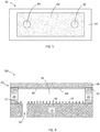
- the device 100 includes a first sidewall 22 and a second sidewall 24 . While shown as separate structures, it will be understood that the first 22 and second 24 sidewalls may be formed from one continuous sidewall. Whether one structure or separate structures, the first 22 and second 24 sidewalls define a fluidic channel 50 .
- the device 100 also includes a bulk acoustic resonator structure 10 having a surface 10 ′ defining at least a portion of the channel 50 .
- a biomolecule 60 is attached to the surface 10 ′ of the resonator structure 10 , such that the biomolecule 60 is in fluid communication with the fluidic channel 50 .
- the target analyte may bind to the biomolecule 60 and add mass to the surface of the resonator structure 10 .
- the change of mass may be transduced by the resonator structure 10 to produce an electrical signal that correlates to the change in mass.
- the biomolecule 60 may be applied to all or a portion of the surface 10 ′ of the resonator structure 10 . If applied to less than all of the surface 10 ′ a blocking material 70 may be applied to those portions of the surface 10 ′ to which the biomolecule 60 is not bound. Further information on processes that may be employed to coat portion of a surface 10 ′ of a resonator structure 10 and to block a portion of a surface 10 ′ of a resonator structure 10 is provided in U.S. patent application Ser. No. 15/334,459, filed on Oct. 26, 2016, which application is hereby incorporated herein by reference in its entirety to the extent that it does not conflict with the disclosure presented herein.
- the biomolecule 60 is attached to the surface 10 ′ in an active zone 16 of the resonator structure 10 , and the blocking material 70 is disposed on less active portions 17 of the surface 10 ′ of the resonator structure 10 . Additional information regarding active zones of resonator structures is described in U.S. patent application Ser. No. 15/334,459, filed on Oct. 26, 2016.
- the device 100 includes a cover 40 having a portion 40 A disposed over the first sidewall 22 , a portion 40 B disposed over the second sidewall 24 , and a portion 40 C disposed over the fluidic channel 50 .
- the cover has in inner surface 40 ′ that defines at least a portion of the channel 50 and has an outer surface 40 ′′.
- the cover 40 includes a first portion 40 A disposed over the first sidewall 22 , has a second portion 40 B disposed over the second sidewall 24 , and has a portion 40 C disposed over the channel 50 .
- the first 40 A and second 40 B portions of the cover 40 are transparent to UV-radiation.
- the portion 40 C of the cover 40 disposed over the channel 50 blocks transmission of UV-radiation.
- a “UV-transparent” portion of a cover means that the cover has a percent transmittance (% T) of 60% T or more of radiant energy having a wavelength in a range from 200 nm to 400 nm.
- the cover may have % T for UV radiation of 80% T or more.
- the cover has a % T of 90% T or more, or 95% T or more.
- a “UV-blocking” portion of a cover means that the cover has a % T of 30% T or less of radiant energy having a wavelength in a range from 200 nm to 400 nm.
- the cover may have a % T for UV radiation of 20% T or less.
- the cover has a % T of 10% T or less, or 5% T or less, 3% T or less, 2% T or less or 1% T or less.
- the cover 40 may be fixed by adhesive 30 disposed on top of the first sidewall 22 and the second sidewall 24 .
- the adhesive 30 may comprise UV-curable adhesive. Exposure of the external surface 40 ′′ of the cover 40 will result in UV radiation being transmitted through the first 40 A and second 40 B portions of the cover to the adhesive to cure the adhesive and bond the cover 40 to the first 22 and second 24 sidewalls, while transmission of the UV radiation through the portion 40 C of the cover over the channel 50 will be blocked to protect the biomolecule 60 attached to the surface 10 ′ of the resonator structure 10 from the potentially damaging effects of the UV radiation.
- the fluidic device 100 includes a cover 40 comprising a UV blocking coating 80 .
- the coating 80 is disposed on an inner surface of a substrate 44 and forms the inner surface 40 ′ of the cover 40 ′.
- a UV-blocking coating is disposed on the outer surface 44 ′′ of the substrate 44 (at portion 40 C) and not on the inner surface of the substrate 44 .
- a UV-blocking coating is disposed on both the outer surface 44 ′′ of the substrate 44 (at portion 40 C) and on the inner surface of the substrate 44 (at portion 40 C).
- the UV-blocking coating 80 is disposed on the inner surface 44 ′ of the substrate 44 (or the inner surface and the outer surface). Having the UV-blocking coating on the inner surface 44 of the substrate 44 allows less angled UV rays to pass through the cover 40 to react with the biomolecule 60 . The closer the coating 80 is to the surface 10 ′ to be protected, the more collimated effect it provides.
- the substrate 44 is transparent to UV-radiation. Any suitable UV-transparent substrate may be employed to form the cover 40 .
- the substrate 44 may comprise UV-transparent glass or UV-transparent polymeric material.
- UV-transparent polymer materials include cyclic olefin copolymers (COC) such as COC sold under the tradename TOPAS®, acrylic polymers, polymethylpentene (PMP), and the like.
- the UV-blocking coating 80 may be transparent to visible light or may block transmission of visible light.
- the coating 80 may comprise one or more compound that absorbs or reflects UV radiation. Examples of compounds that absorb UV radiation include benzophenone, benzophenone derivatives, or other phenol containing compound that absorbs UV light and certain metal oxides such as zinc oxide, titanium oxide, silicon oxide and cerium oxide. In some embodiments, nano-sized particles of one or more metal oxide are used.
- the one or more UV-absorbing compounds may be incorporated into a polymeric material and coated on the surface of the substrate 44 to block transmission of UV radiation through the portion 40 C of the cover 40 configured to be disposed over the microfluidic channel 50 .
- coatings 80 that reflect UV radiation include metallic coatings, such as chrome coatings, aluminum coatings, and duralumin coatings. Metal oxides, such as those described above, may also serve to reflect UV radiation. In addition, stacking, thickness and index matching of layers of a multilayer cover may be varied to permit or block transmission of UV radiation.
- the UV-blocking coating 80 may be applied to the substrate 44 in any suitable manner.
- the UV blocking material may be applied by a process including, but not limited to, spray coating, float coating, plasma deposition, vapor deposition, and sputtering.
- the first 40 A and second 40 B portions of the cover 40 may be masked as the portion 40 C of the cover 40 configured to be disposed over the channel 50 is coated.
- the mask may be removed, leaving the first 40 A and second 40 B uncoated portions transparent to UV radiation due to the transparent nature of the substrate 44 , while the coated portion 40 C of the cover 40 exhibits UV blocking properties due to the UV-blocking coating 80 .
- the cover 40 may be a cover as shown in FIG. 2 .
- the cover 40 depicted in FIG. 3 includes a UV-transparent substrate 44 on which a UV-blocking coating 80 is disposed.
- the coating 80 is disposed on a region (e.g., region 40 C depicted in FIG. 2 ) configured to be disposed over the channel (e.g., channel 50 depicted in FIG. 2 ).
- the coating 80 is not disposed on the periphery of the substrate 44 so that the outer regions (e.g., regions 40 A and 40 B depicted in FIG.
- sidewalls e.g., sidewalls 22 , 24 depicted in FIG. 2
- sidewalls e.g., sidewalls 22 , 24 depicted in FIG. 2
- adhesive e.g., adhesive 30
- FIG. 4 a schematic cross section of a microfluidic sensor device 100 is depicted.
- the device 100 contains components similar to the devices depicted in FIGS. 1 and 2 .
- the cover 40 depicted in FIG. 4 defines first 92 and second 94 ports, which may serve as an inlet and outlet for microfluidic channel 50 .
- the ports 92 , 94 are disposed over portions 17 of the resonator structure 10 to which blocking material 70 , rather than biomolecule 60 , is disposed.
- the cover 40 includes a UV blocking coating 80 on a region disposed over the region 16 of the surface 10 ′ of the resonator structure 10 to which the biomolecule 60 is bound to protect the biomolecule from UV radiation used to cure the adhesive 30 .
- the cover 40 may be a cover as shown in FIG. 4 .
- the cover 40 depicted in FIG. 5 includes a UV-transparent substrate 44 on which a UV-blocking coating 80 is disposed.
- the coating 80 is disposed on a region configured to be disposed over the channel (e.g., channel 50 depicted in FIG. 4 ), particularly over a region (e.g., region 16 of FIG. 4 ) of the surface of the resonator structure to which biomolecule is attached.
- the channel e.g., channel 50 depicted in FIG. 4
- region 16 of FIG. 4 e.g., region 16 of FIG. 4
- the coating 80 is not disposed on the periphery of the substrate 44 so that the outer regions configured to be disposed over the sidewalls (e.g., sidewalls 22 , 24 depicted in FIG. 4 ) are transparent to UV radiation, so that UV radiation may be transmitted through the substrate 44 to adhesive (e.g., adhesive 30 ) disposed on top of the sidewalls.
- the cover 40 defines ports 92 , 94 through the substrate 44 , which are preferably configured to be disposed over a less active region (e.g. region 17 depicted in FIG. 4 ) of the surface of the substrate or over a region of the substrate on which blocking material (e.g., blocking material 70 depicted in FIG. 4 ) is disposed.
- FIG. 6 a schematic cross section of a microfluidic sensor device 100 is depicted.
- the device 100 contains components similar to the devices depicted in FIGS. 1, 2, and 4 .
- the via 95 is defined through the resonator structure 10 .
- the via 95 may serve as an inlet or an outlet to the microfluidic channel. More than one via may be formed through the resonator structure 95 to provide access to the channel 50 .
- an inlet or outlet to the microfluidic channel is shown in cover in FIG. 2 and in the resonator structure in FIG. 4 , it will be understood that an inlet or outlet into the microfluidic channel may be formed in any suitable manner or through any suitable structure, such as through a sidewall.
- FIGS. 7A-7F a brief overview of an example of an embodiment of a process for fabricating a microfluidic sensing device is shown.
- a resonator structure 10 is provided. Additional details regarding one way to fabricate an embodiment of such a resonator structure are described below with reference to FIGS. 8-9 .
- sidewalls 22 , 24 are positioned on the resonator structure 10 . A discussed above, the sidewalls 22 , 24 may be formed from one continuous structure or from separate structures.
- Sidewalls 22 , 24 may be formed of any suitable material, such as a laser-cut “stencil” layer of thin polymeric materials and/or laminate materials, optionally including one or more self-adhesive surfaces (e.g. adhesive tape), or using an SU-8 negative epoxy resist or other photoresist material.
- a laser-cut “stencil” layer of thin polymeric materials and/or laminate materials optionally including one or more self-adhesive surfaces (e.g. adhesive tape), or using an SU-8 negative epoxy resist or other photoresist material.
- biomolecule 60 is applied to a surface 10 ′ of the resonator structure 10 .
- the surface 10 ′ of the resonator structure 10 or a portion thereof may be chemically functionalized or activated for binding to a deposited biomolecule 60 .
- a layer (not shown) comprising a functional material for binding to the biomolecule 60 may be deposited on the surface 10 ′, or a portion thereof, to activate the surface for binding the biomolecule 60 .
- the surface 10 ′ may be functionalized to including a hydroxylated oxide surface suitable for attachment of an organosilane-based SAM, or comprises gold or another noble metal suitable for attachment of a thiol-based self-assembled monolayer (SAM). Following formation of the SAM, biomolecule 60 may be deposited on the SAM.
- a UV-curable adhesive 32 may be applied to the top of the first 22 and second 24 sidewalls. Any suitable UV-curable adhesive 32 may be applied.
- the UV-curable adhesive may include an adhesive resin and a UV photoactivator, such as a free-radical activator.
- the UV-curable adhesive is a UV-curable epoxy. UV curable adhesives are commercially available from a number of manufacturers, such as Henkel, MasterBond, Parson Adhesives, Inc., and Epoxies Innovative Bonding Solutions, Etc.
- a UV-curable adhesive 32 may be applied to regions 40 A and 40 B of the cover 40 on surface 40 ′ (not shown) to avoid the possibility of stray droplets of adhesive from landing on the surface 10 ′ of the resonator structure 10 .
- a cover 40 having a UV-transparent substrate 44 and a UV blocking coating 80 may be disposed on the UV-curable adhesive 32 on top of the first 22 and second 24 sidewalls (alternatively, a cover 40 to which adhesive 32 is applied to regions 40 A and 40 B may be placed on the sidewalls 22 , 24 ).
- First 40 A and second 40 B portions of the cover 40 are transparent (e.g., not coated) to UV-radiation and a coated portion 40 C blocks transmission of UV coating through the cover 40 .
- the first 40 A and second 40 B portions of the cover 40 are aligned with the first 22 and second 24 sidewalls and the blocked portion 40 is disposed over the channel 50 . UV radiation (indicated by vertical arrows in FIG.
- the cover 40 may be applied external to the cover 40 and be transmitted through the first 40 A and second 40 B portions to allow the UV radiation to cure the UV-curable adhesive.
- the source of UV radiation may be a broadband source or a narrow band source.
- the cured adhesive 30 bonds the cover 40 to the sidewalls 22 , 24 .
- the UV-radiation is blocked from passing through cover 40 in region 40 C due to the UV-blocking coating 80 , which protects the biomolecule 80 attached to the surface 10 ′ of the resonator structure 10 .
- UV-exposure and UV-curing may be performed at temperatures below, for example, 40° C. (or any other suitable temperature) so that the biomolecules 60 are not subjected to temperatures that may denature or otherwise adversely affect properties of the biomolecules 60 .
- the description provided above is fairly generic regarding a resonator structure. Some of the description provided below details embodiments of bulk acoustic resonators that may be employed as a resonator structure.
- the resonator structure comprises a BAW resonator structure arranged over at least a portion of a substrate, and a biomolecule arranged over at least a portion of an active region of the BAW resonator structure.
- a top side electrode which is coincident with an active region of a BAW resonator structure
- a hermeticity layer e.g., to protect the top side electrode from corrosion in a liquid environment
- an interface layer e.g., to protect the top side electrode from corrosion in a liquid environment
- SAM self-assembled monolayer
- the interface layer facilitates attachment of an overlying SAM
- the SAM facilitates attachment of an overlying functionalization material.
- FIG. 8 is a schematic cross-sectional view of a portion of a bulk acoustic wave MEMS resonator structure 10 useable with embodiments disclosed herein.
- the resonator structure 10 includes a substrate 132 (e.g., typically silicon or another semiconductor material), an acoustic reflector 134 arranged over the substrate 132 , a piezoelectric material 142 , and bottom and top side electrodes 140 , 148 .
- the bottom side electrode 140 is arranged along a portion of a lower surface 144 of the piezoelectric material 142 (between the acoustic reflector 134 and the piezoelectric material 142 ), and the top side electrode 148 is arranged along a portion of an upper surface 146 of the piezoelectric material 142 .
- An area in which the piezoelectric material 142 is arranged between overlapping portions of the top side electrode 148 and the bottom side electrode 140 is considered an active region 16 of the resonator device 10 to which a biomolecule is preferably applied.
- the acoustic reflector 134 serves to reflect acoustic waves and therefore reduce or avoid their dissipation in the substrate 132 .
- the acoustic reflector 134 includes alternating thin layers 136 , 138 of materials (e.g., silicon oxicarbide [SiOC], silicon nitride [Si 3 N 4 ], silicon dioxide [SiO 2 ], aluminum nitride [AlN], tungsten [W], and molybdenum [Mo]) having different acoustic impedance values, optionally embodied in a quarter-wave Bragg mirror, deposited over the substrate 132 .
- materials e.g., silicon oxicarbide [SiOC], silicon nitride [Si 3 N 4 ], silicon dioxide [SiO 2 ], aluminum nitride [AlN], tungsten [W], and molybdenum [Mo]
- SiOC silicon oxicarbide
- Si 3 N 4 silicon dioxide
- AlN aluminum nitride
- W tungsten
- Mo molybdenum
- Steps for forming the resonator device 30 may include depositing the acoustic reflector 134 over the substrate 132 , followed by deposition of the bottom side electrode 140 , followed by growth (e.g., via sputtering or other appropriate methods) of the piezoelectric material 142 , followed by deposition of the top side electrode 148 .
- the piezoelectric material 142 comprises a hexagonal crystal structure piezoelectric material (e.g., aluminum nitride or zinc oxide) that includes a c-axis having an orientation distribution that is predominantly non-parallel (and may also be non-perpendicular to) to normal of a face of the substrate 132 .
- a hexagonal crystal structure piezoelectric material e.g., aluminum nitride or zinc oxide
- the piezoelectric material 142 comprises a hexagonal crystal structure piezoelectric material (e.g., aluminum nitride or zinc oxide) that includes a c-axis having an orientation distribution that is predominantly non-parallel (and may also be non-perpendicular to) to normal of a face of the substrate 132 .
- a BAW resonator structure Under appropriate conditions, presence of a c-axis having an orientation distribution that is predominantly non-parallel to normal of a face of a substrate enables a BAW resonator structure to be configured to exhibit a dominant shear response upon application of an alternating current signal across a distal electrode and a proximal electrode thereof (e.g., as may be desirable in the context of a BAW resonator structure providing sensing utility).
- Methods for forming hexagonal crystal structure piezoelectric materials including a c-axis having an orientation distribution that is predominantly non-parallel to normal of a face of a substrate are disclosed in U.S.
- the bulk acoustic wave MEMS resonator structure 10 shown in FIG. 8 lacks any layers (e.g., including functionalization material) overlying the active region 16 that would permit the resonator device 10 to be used as a biochemical sensor. If desired, at least portions of the resonator device 10 shown in FIG. 8 (e.g., including the active region 16 ) may be overlaid with various layers, such as one or more of: a hermeticity layer, an interface layer, a self-assembled monolayer (SAM), and/or a functionalization material layer (which may include specific binding material or non-specific binding material).
- a hermeticity layer such as one or more of: a hermeticity layer, an interface layer, a self-assembled monolayer (SAM), and/or a functionalization material layer (which may include specific binding material or non-specific binding material).
- SAM self-assembled monolayer
- FIG. 9 is a schematic cross-sectional view of an upper portion of a BAW resonator device including a piezoelectric material 142 and a top side electrode 148 overlaid with a hermeticity layer 152 , an interface layer 154 , a self-assembled monolayer (SAM) 156 , and a layer 158 comprising a biomolecule.
- one or more blocking materials may be applied during fabrication, such as over portions of an interface layer to prevent localized attachment of one or more subsequently deposited layers, or (if applied over selected regions of a SAM or a functionalization material) to prevent analyte capture in regions not overlying an active region of the BAW resonator device.
- photolithography may be used to promote patterning of interface material or blocking material over portions of a MEMS resonator device.
- Photolithography involves use of light to transfer a geometric pattern from a photomask to a light-sensitive chemical photoresist on a substrate and is a process well known to those of ordinary skill in the semiconductor fabrication art. Typical steps employed in photolithography include wafer cleaning, photoresist application (involving either positive or negative photoresist), mask alignment, and exposure and development.
- an interface layer may be patterned by etching in one or more gaps in a photoresist layer, and the photoresist layer may be subsequently removed (e.g., using a liquid photoresist stripper, by ashing via application of an oxygen-containing plasma, or another removal process).
- an interface layer (e.g., arrangeable between a top side electrode and a SAM) includes a hydroxylated oxide surface suitable for formation of an organosilane SAM.
- a preferred interface layer material including a hydroxylated oxide surface is silicon dioxide (SiO 2 ).
- Alternative materials incorporating hydroxylated oxide surfaces for forming interface layers include silicon dioxide [SiO 2 ], titanium dioxide [TiO 2 ], tantalum pentoxide [Ta 2 O 5 ], hafnium oxide [HfO 2 ], or aluminum oxide [Al 2 O 3 ].
- Other alternative materials incorporating hydroxylated oxide surfaces will be known to those skilled in the art, and these alternatives are considered to be within the scope of the present disclosure.
- an interface layer (e.g., arrangeable between a top side electrode and a SAM), or at least one electrode that is devoid of an overlying interface layer, includes gold or another noble metal (e.g., ruthenium, rhodium, palladium, osmium, iridium, platinum, or silver) suitable for receiving a thiol-based SAM that may be overlaid with functionalization material.
- gold or another noble metal e.g., ruthenium, rhodium, palladium, osmium, iridium, platinum, or silver
- a hermeticity layer may be applied between a top side electrode and an interface layer.
- a hermeticity layer may be unnecessary when noble metals (e.g., gold, platinum, etc.) are used for top side electrodes.
- a hermeticity layer preferably includes a dielectric material with a low water vapor transmission rate (e.g., no greater than 0.1 g/m 2 /day).
- a SAM may be formed over the interface layer, with the SAM including an organosilane material in certain embodiments.
- the hermeticity layer protects a reactive electrode material (e.g., aluminum or aluminum alloy) from attack in corrosive liquid environments, and the interface layer facilitates proper chemical binding of the SAM.
- a hermeticity layer and/or an interface layer may be applied via one or more deposition processes such as atomic layer deposition (ALD), chemical vapor deposition (CVD), or physical vapor deposition (PVD).
- ALD is preferred for deposition of at least the hermeticity layer (and may also be preferable for deposition of the interface layer) due to its ability to provide excellent conformal coating with good step coverage over device features so as to provide layer structures that are free of pinholes.
- ALD is capable of forming uniformly thin layers that provide relatively little damping of acoustic vibrations that would otherwise result in degraded device performance.
- Adequacy of coverage may be important for a hermeticity layer (if present) to avoid corrosion of the underlying electrode.
- ALD chemical vapor deposition, or any other suitable deposition process may be used to apply the hermeticity layer.
- an interface layer may be deposited.
- a hermeticity layer and an interface layer may be sequentially applied in a vacuum environment, thereby promoting a high-quality interface between the two layers. If multiple layers are deposited, they may be deposited sequentially without breaking vacuum, or may be applied separately with vacuum break.
- a hermeticity layer may include an oxide, a nitride, or an oxynitride material serving as a dielectric material and having a low water vapor transmission rate (e.g., no greater than 0.1 g/m 2 /day) according to certain embodiments.
- a hermeticity layer includes at least one of aluminum oxide (Al 2 O 3 ) or silicon nitride (SiN).
- an interface layer includes at least one of SiO 2 , TiO 2 , or Ta 2 O 5 .
- multiple materials may be combined in a single hermeticity layer, and/or a hermeticity layer may include multiple sublayers of different materials.
- a hermeticity layer is further selected to promote compatibility with an underlying reactive metal (e.g., aluminum or aluminum alloy) electrode structure of an acoustic resonator structure.
- an underlying reactive metal e.g., aluminum or aluminum alloy
- aluminum or aluminum alloys are frequently used as electrode materials in BAW resonator structures, various transition and post-transition metals can be used for such electrodes.
- a SAM is preferably formed over the interface layer.
- SAMs are typically formed by exposure of a solid surface to amphiphilic molecules with chemical groups that exhibit strong affinities for the solid surface.
- organosilane SAMs are particularly preferred for attachment to the hydroxylated oxide surface.
- Organosilane SAMs promote surface bonding through silicon-oxygen (Si—O) bonds. More specifically, organosilane molecules include a hydrolytically sensitive group and an organic group and are therefore useful for coupling inorganic materials to organic polymers.
- An organosilane SAM may be formed by exposing a hydroxylated oxide surface to an organosilane material in the presence of trace amounts of water to form intermediate silanol groups. These groups then react with free hydroxyl groups on the hydroxylated surface to covalently immobilize the organosilane.
- organosilane-based SAMs that are compatible with interface layers incorporating hydroxylated oxide surfaces include 3-glycidoxypropyltrimethoxysilane (GPTMS), 3-mercaptopropyltrimethoxysilane (MPTMS), 3-aminopropyltrimethoxysilane (APTMS), and octadecyltrimethoxysilane (OTMS), including their ethoxy- and chloro-variants.
- Additional silanes that may be used for SAMs include poly(ethylene glycol) (PEG) conjugated variants.
- An exemplary SAM may include a thickness in a range of at least 0.5 nm or more.
- a SAM readily binds to the locally patterned interface layer but does not readily bind to other adjacent material layers (e.g., a hermeticity layer, a piezoelectric material, and/or a blocking material layer).
- thiol-based SAMs may be used.
- Alkanethiols are molecules with an alkyl chain as the back bone, a tail group, and an S—H head group.
- Thiols may be used on noble metal interface layers due to the strong affinity of sulfur for these metals. Examples of thiol-based SAMs that may be used include, but are not limited to, 1-dodecanethiol (DDT), 11-mercaptoundecanoic acid (MUA), and hydroxyl-terminated (hexaethylene glycol) undecanethiol (1-UDT).
- DDT 1-dodecanethiol
- UAA 11-mercaptoundecanoic acid
- 1-UDT hydroxyl-terminated (hexaethylene glycol) undecanethiol
- SAMs contain the same backbone, but different end groups—namely, methyl (CH 3 ), carboxyl (COOH), and hydroxyl-terminated hexaethylene glycol (HO—(CH 2 CH 2 O) 6 ) for DDT, MUA, and 1-UDT, respectively.
- SAMs may be formed by incubating gold surfaces in thiol solutions using a suitable solvent, such as anhydrous ethanol.
- the SAM may be biologically functionalized, such as by receiving at least one specific binding material.
- specific binding materials may be applied on or over a SAM using a microarray spotting needle or other suitable methods.
- an interface layer may be patterned (e.g., using photolithography for defining the interface layer) with a high dimensional tolerance over only a portion of a resonator structure (which includes a substrate), a SAM may be applied over the interface layer, and a subsequently applied specific binding material may be attached only to the SAM.
- patterning of an interface layer may provide a higher dimensional tolerance for positioning of the specific binding material than could be attained by microarray spotting alone.
- specific binding materials include, but are not limited to, antibodies, receptors, ligands, and the like.
- a specific binding material is preferably configured to receive a predefined target species (e.g., molecule, protein, DNA, virus, bacteria, etc.).
- a functionalization material including specific binding material may include a thickness in a range of from about 5 nm to about 1000 nm, or from about 5 nm to about 500 nm.
- an array of different specific binding materials may be provided over different active areas of a multi-resonator structure (i.e., one or more resonator structures including multiple active regions), optionally in combination with one or more active areas that are devoid of specific binding materials to serve as comparison (or “reference”) regions.
- a functionalization material e.g., chemical functionalization material
- Certain embodiments are directed to a fluidic device including multiple bulk acoustic wave MEMS resonator structures as disclosed herein and including a fluidic passage (e.g., a channel, a chamber, or the like) arranged to conduct a liquid to contact at least one functionalization (e.g., specific binding) material arranged over at least one active region of the resonator structures.
- a fluidic passage e.g., a channel, a chamber, or the like
- Such a device may be microfluidic in scale, and comprise at least one microfluidic passage (e.g., having at least one dimension, such as height and/or width, of no greater than about 1000 microns, no greater than about 500 microns, or no greater than about 250 microns, or no greater than about 100 microns).
- a microfluidic device may be fabricated by forming one or more walls defining lateral boundaries of a microfluidic channel over a first bulk acoustic wave MEMS resonator structure with an active region thereof arranged along a bottom surface of a microfluidic passage, and then enclosing the microfluidic passage using a cap or cover layer that may define fluidic ports (e.g., openings) enabling fluid communication with the microfluidic passages.
- fluidic ports e.g., openings
- functionalization (e.g., specific binding) material may be pre-applied to the active region of a bulk acoustic wave MEMS resonator structure before formation of a microfluidic passage; in other embodiments, functionalization material may be applied over an active region of a bulk acoustic wave resonator structure following formation of the microfluidic passage.
- Walls of a microfluidic channel may be formed of any suitable material, such as laser-cut “stencil” layers of thin polymeric materials and/or laminate materials, optionally including one or more self-adhesive surfaces (e.g., adhesive tape).
- such walls may be formed prior to deposition of a SAM layer, functionalization material, and/or blocking layers, with an SU-8 negative epoxy resist or other photoresist material.
- a cover or cap layer may be integrally formed with one or more walls (e.g., via molding or another suitable process) to define a portion of an upper boundary as well as lateral boundaries of at least one fluidic channel, and the integrally formed partial cover/wall structure may be applied (e.g., adhered or otherwise bonded) over at least a portion of a bulk acoustic wave resonator structure to enclose the at least one fluidic channel.
- a chemical or biological blocking material may be applied over a portion of a SAM to prevent attachment of a functionalization (e.g., specific binding) material over one or more selected regions of a BAW resonator structure (e.g., one or more regions apart from an active region).
- a chemical or biological blocking material e.g., blocking buffer
- Various types of blocking buffers such as highly purified proteins, serum, or milk may be used to block free sites on a SAM. Additional blockers include ethanolamine or polyethylene oxide (PEO)—containing materials.
- An ideal blocking buffer would bind to all potential sites of non-specific interaction away from an active region. To optimize a blocking buffer for a particular analysis, empirical testing may be used to determine signal-to-noise ratio. No single chemical blocking material is ideal for every situation, since each antibody-antigen pair has unique characteristics.
- FIG. 10 is a perspective assembly view of a microfluidic device 190 incorporating a substrate 102 with multiple bulk acoustic wave MEMS resonator devices, an intermediate layer 120 defining a central microfluidic channel 122 registered with active regions 108 A- 108 N (to which biomolecule is attached) of the MEMS resonator devices, and a cap or cover layer 130 arranged to cover the intermediate layer 120 .
- Top central portions of the substrate 102 which includes an acoustic reflector (not shown) and a piezoelectric material (not shown), include a top side electrode 106 and bottom side electrodes 104 A- 104 N.
- Regions in which the foregoing electrodes overlap one another with the piezoelectric material arranged therebetween embody active regions 108 A- 108 N. Any suitable number of active regions 108 A- 108 N may be provided and fluidically arranged in series or parallel, although five active regions are illustrated in FIG. 10 .
- Top peripheral (or top end) portions of the substrate 102 further include reference top side electrodes 116 and reference bottom side electrodes 114 in communication with reference overlap regions 110 . Such reference overlap regions 110 are not exposed to fluid, and are present to provide a basis for comparing signals obtained from the active regions 108 A- 108 N exposed to fluid within the central microfluidic channel 122 .
- the substrate 102 is overlaid with the intermediate (e.g., wall-defining) layer 120 , wherein the central microfluidic channel 122 is intended to receive fluid, and defines peripheral chambers 124 arranged to overlie the reference overlap regions 110 in a sealed fashion.
- the intermediate layer 120 may be formed of any suitable material such as SU-8 negative epoxy resist, other photoresist material, or laser-cut “stencil” layers of thin polymeric materials optionally including one or more self-adhesive surfaces (e.g., adhesive tape), etc.
- the intermediate layer 120 further includes a lateral inset region 126 that enables lateral portions of the top side electrode 106 and bottom side electrodes 104 A- 104 N to be accessed upon assembly of the microfluidic device 100 .
- the cap or cover layer 130 includes a lateral inset region 136 registered with the lateral inset region 126 of the intermediate layer 120 , and includes microfluidic ports 132 , 134 accessible along a top surface 138 and registered with end portions of the central microfluidic channel 122 defined in the intermediate layer 120 to permit fluid (e.g., liquid) to be supplied to the central microfluidic channel 122 over the active regions 108 A- 108 N.
- fluid e.g., liquid
- at least the electrodes 104 A- 104 N, 106 are overlaid with a hermeticity layer, an interface layer, a self-assembled monolayer, and biomolecule for binding analyte as disclosed herein.
- Microfluidic devices according to other configurations may be provided, as will be recognized by those skilled in the art upon review of the present disclosure.
- FIGS. 11-13 shows that the aforementioned methods can also be applied to wafer-level bonding for wafer-level packaging (WLP).
- WLP wafer-level packaging
- FIG. 11 depicts a wafer 300 that may be cut into a number of dies, each containing a resonator structure 10 as described above.
- the wafer 300 includes a plurality of walls 220 , 240 extending from the surface of the wafer. When the wafer 300 is cut into dies, walls 220 , 240 may serve as sidewalls of the die (e.g., sidewalls 22 , 24 described above).
- the biomolecule e.g., biomolecule 60 described above
- the cover 400 includes a number of UV-blocked regions 400 C and UV-transparent areas 400 A, 400 B (which correspond to depicted vertical and horizontal lines).
- the UV-transparent regions 400 A, 400 B may be aligned with walls 220 , 240 of wafer 300
- UV-blocked regions 400 C may be aligned with what will result in resonator structures 10 of wafer when the wafer is cut into dies.
- FIG. 13 depicts a structure 500 that includes the cover 400 bonded to the wafer 300 in a manner such that the UV-transparent regions 400 A, 400 B of the cover 400 are aligned with walls 220 , 240 of wafer 300 .
- UV-curable adhesive may be applied to the UV-transparent regions 400 A, 400 B of the cover 400 , and the cover 400 may be placed on the wafer 300 such that the adhesive (not shown) is aligned with the tops of the walls 220 , 240 of the wafer 300 .
- the resulting structure 500 may be exposed to UV radiation to cure the adhesive and bond the cover 400 to the wafer 300 .
- the resulting structure 500 may be cut along the shown lines (corresponding to walls 220 , 240 of wafer 300 and UV-transparent regions 400 A, 400 B of cover 400 ) to generate a number of fluid sensing devices 100 (e.g., devices 100 as depicted and described with regard to FIGS. 1, 2, 4, 6, and 7F above).
- fluid sensing devices 100 e.g., devices 100 as depicted and described with regard to FIGS. 1, 2, 4, 6, and 7F above).
- FIGS. 14A-J For purposes of illustration of wafer-level packing, reference is now made to FIGS. 14A-J .
- FIG. 14A a cross sectional view of a wafer 300 is shown.
- walls 220 are deposited on a surface of the wafer 300 .
- Biomolecule 60 is deposited on the surface of the wafer 300 between the walls 220 ( FIG. 14C ).
- a wafer-scale cover 400 is depicted.
- the cover 400 is UV-transparent.
- a UV-blocking coating 480 is deposited on a surface of the cover 400 (e.g. in region 400 C depicted in FIG. 12 ).
- UV-curable adhesive 430 is deposited on the surface of the cover 400 between the UV-blocking coating 480 (e.g., the adhesive 430 is deposited in regions 400 A, 400 B depicted in FIG. 12 ).
- the cover 400 may be inverted and placed on the wafer 300 such that the adhesive 430 is disposed on top of the walls 220 and the coating 480 is disposed over the region of the wafer 300 on which the biomolecule 60 is deposited.
- UV radiation (indicated by vertical arrows) may be applied external to the cover 400 .
- the UV radiation is transmitted through the UV transparent areas of the cover 400 on which the adhesive 430 is deposited (e.g., regions 400 A, 400 B depicted in FIG. 12 ). UV-radiation is blocked by coating 80 to protect the biomolecule 60 .
- the resulting structure 500 which may be cut into individual fluid sensing devices 100 is shown in FIG. 14I .
- the resulting structure 500 may be cut along lines corresponding to walls 220 of wafer 300 and UV-transparent regions of cover 400 (e.g., the resulting structure 500 may be cut along lines corresponding to walls 220 , 240 shown in FIG. 11 ).
- FIG. 14I A fluid sensing device 100 resulting from cutting of a wafer-scale device 500 is depicted in FIG. 14I , which may correspond to devices 100 as depicted and described with regard to FIGS. 1, 2, 4, 6, and 7F above.
- FIG. 14J For the numbered elements depicted in FIG. 14J , reference is made to the description above regarding FIGS. 1, 2, 4, 6, and 7F .
- any direction referred to herein, such as “top,” “bottom,” “left,” “right,” “upper,” “lower,” and other directions and orientations are described herein for clarity in reference to the figures and are not to be limiting of an actual device or system or use of the device or system. Devices or systems as described herein may be used in a number of directions and orientations.
- providing in the context of providing an article or a device means to make, purchase, or otherwise obtain the article or device.
Landscapes
- Health & Medical Sciences (AREA)
- Physics & Mathematics (AREA)
- Chemical & Material Sciences (AREA)
- Immunology (AREA)
- Acoustics & Sound (AREA)
- Life Sciences & Earth Sciences (AREA)
- Analytical Chemistry (AREA)
- General Health & Medical Sciences (AREA)
- Engineering & Computer Science (AREA)
- Hematology (AREA)
- General Physics & Mathematics (AREA)
- Pathology (AREA)
- Biochemistry (AREA)
- Biomedical Technology (AREA)
- Urology & Nephrology (AREA)
- Molecular Biology (AREA)
- Chemical Kinetics & Catalysis (AREA)
- Clinical Laboratory Science (AREA)
- Dispersion Chemistry (AREA)
- Manufacturing & Machinery (AREA)
- Biotechnology (AREA)
- Cell Biology (AREA)
- Microbiology (AREA)
- Food Science & Technology (AREA)
- Medicinal Chemistry (AREA)
- Micromachines (AREA)
- Fluid Mechanics (AREA)
Abstract
Description
Claims (12)
Priority Applications (1)
| Application Number | Priority Date | Filing Date | Title |
|---|---|---|---|
| US15/470,111 US10659000B2 (en) | 2016-03-25 | 2017-03-27 | Fluidic sensor device having UV-blocking cover |
Applications Claiming Priority (2)
| Application Number | Priority Date | Filing Date | Title |
|---|---|---|---|
| US201662313301P | 2016-03-25 | 2016-03-25 | |
| US15/470,111 US10659000B2 (en) | 2016-03-25 | 2017-03-27 | Fluidic sensor device having UV-blocking cover |
Publications (2)
| Publication Number | Publication Date |
|---|---|
| US20170294892A1 US20170294892A1 (en) | 2017-10-12 |
| US10659000B2 true US10659000B2 (en) | 2020-05-19 |
Family
ID=59998339
Family Applications (1)
| Application Number | Title | Priority Date | Filing Date |
|---|---|---|---|
| US15/470,111 Active 2038-06-25 US10659000B2 (en) | 2016-03-25 | 2017-03-27 | Fluidic sensor device having UV-blocking cover |
Country Status (1)
| Country | Link |
|---|---|
| US (1) | US10659000B2 (en) |
Cited By (1)
| Publication number | Priority date | Publication date | Assignee | Title |
|---|---|---|---|---|
| CN113258900A (en) * | 2021-06-23 | 2021-08-13 | 深圳汉天下微电子有限公司 | Bulk acoustic wave resonator assembly, preparation method and communication device |
Families Citing this family (6)
| Publication number | Priority date | Publication date | Assignee | Title |
|---|---|---|---|---|
| US10371667B2 (en) * | 2015-11-16 | 2019-08-06 | Qorvo Us, Inc. | BAW sensor with passive mixing structures |
| US11099157B2 (en) | 2018-07-06 | 2021-08-24 | Qorvo Biotechnologies, Llc | Sensor with droplet retaining structure |
| DE102018118581A1 (en) * | 2018-07-31 | 2020-02-06 | Lohmann Gmbh & Co. Kg | Cartridge cover device for sealing a microfluidic cartridge |
| US11325121B2 (en) | 2019-03-29 | 2022-05-10 | Qorvo Us, Inc. | Analyte depletion for sensor equilibration |
| CN111001452B (en) * | 2019-12-20 | 2022-04-05 | 京东方科技集团股份有限公司 | Miniature full-analysis device and manufacturing method thereof |
| CN112697262B (en) * | 2020-12-08 | 2023-06-27 | 联合微电子中心有限责任公司 | Hydrophone and method for manufacturing same |
Citations (3)
| Publication number | Priority date | Publication date | Assignee | Title |
|---|---|---|---|---|
| US4640756A (en) | 1983-10-25 | 1987-02-03 | The United States Of America As Represented By The United States Department Of Energy | Method of making a piezoelectric shear wave resonator |
| US20170052174A1 (en) * | 2015-08-17 | 2017-02-23 | Sandia Corporation | Shear horizontal surface acoustic wave (sh-saw) resonators and arrays thereof |
| US20170110300A1 (en) | 2015-10-14 | 2017-04-20 | Qorvo Us, Inc. | Deposition system for growth of inclined c-axis piezoelectric material structures |
-
2017
- 2017-03-27 US US15/470,111 patent/US10659000B2/en active Active
Patent Citations (3)
| Publication number | Priority date | Publication date | Assignee | Title |
|---|---|---|---|---|
| US4640756A (en) | 1983-10-25 | 1987-02-03 | The United States Of America As Represented By The United States Department Of Energy | Method of making a piezoelectric shear wave resonator |
| US20170052174A1 (en) * | 2015-08-17 | 2017-02-23 | Sandia Corporation | Shear horizontal surface acoustic wave (sh-saw) resonators and arrays thereof |
| US20170110300A1 (en) | 2015-10-14 | 2017-04-20 | Qorvo Us, Inc. | Deposition system for growth of inclined c-axis piezoelectric material structures |
Non-Patent Citations (1)
| Title |
|---|
| U.S. Appl. No. 15/334,459, filed Oct. 26, 2016, Ryder et al. |
Cited By (2)
| Publication number | Priority date | Publication date | Assignee | Title |
|---|---|---|---|---|
| CN113258900A (en) * | 2021-06-23 | 2021-08-13 | 深圳汉天下微电子有限公司 | Bulk acoustic wave resonator assembly, preparation method and communication device |
| CN113258900B (en) * | 2021-06-23 | 2021-10-15 | 深圳汉天下微电子有限公司 | Bulk acoustic wave resonator assembly, preparation method and communication device |
Also Published As
| Publication number | Publication date |
|---|---|
| US20170294892A1 (en) | 2017-10-12 |
Similar Documents
| Publication | Publication Date | Title |
|---|---|---|
| US10659000B2 (en) | Fluidic sensor device having UV-blocking cover | |
| US10618045B2 (en) | Sensor device with BAW resonator and through-substrate fluidic vias | |
| US11695384B2 (en) | Acoustic resonator device with controlled placement of functionalization material | |
| EP3365669B1 (en) | Resonator structure with enhanced reflection of shear and longitudinal modes of acoustic vibrations | |
| EP3371583B1 (en) | Acoustic resonator devices and fabrication methods providing hermeticity and surface functionalization | |
| EP3427043B1 (en) | Baw sensor fluidic device with increased dynamic measurement range | |
| US10352904B2 (en) | Acoustic resonator devices and methods providing patterned functionalization areas | |
| US10458982B2 (en) | Fluidic device including BAW resonators along opposing channel surfaces | |
| US11940415B2 (en) | Fluidic device with fluid port orthogonal to functionalized active region | |
| US11353428B2 (en) | BAW sensor device with peel-resistant wall structure | |
| US20240230594A1 (en) | Crowded sensor |
Legal Events
| Date | Code | Title | Description |
|---|---|---|---|
| AS | Assignment |
Owner name: QORVO US, INC., NORTH CAROLINA Free format text: ASSIGNMENT OF ASSIGNORS INTEREST;ASSIGNOR:DIEP, BUU QUOC;REEL/FRAME:042743/0868 Effective date: 20170614 |
|
| STPP | Information on status: patent application and granting procedure in general |
Free format text: DOCKETED NEW CASE - READY FOR EXAMINATION |
|
| AS | Assignment |
Owner name: QORVO BIOTECHNOLOGIES, LLC, MINNESOTA Free format text: ASSIGNMENT OF ASSIGNORS INTEREST;ASSIGNOR:QORVO US, INC.;REEL/FRAME:047794/0087 Effective date: 20181204 |
|
| STPP | Information on status: patent application and granting procedure in general |
Free format text: RESPONSE TO NON-FINAL OFFICE ACTION ENTERED AND FORWARDED TO EXAMINER |
|
| STPP | Information on status: patent application and granting procedure in general |
Free format text: NON FINAL ACTION MAILED |
|
| STPP | Information on status: patent application and granting procedure in general |
Free format text: RESPONSE TO NON-FINAL OFFICE ACTION ENTERED AND FORWARDED TO EXAMINER |
|
| STPP | Information on status: patent application and granting procedure in general |
Free format text: NOTICE OF ALLOWANCE MAILED -- APPLICATION RECEIVED IN OFFICE OF PUBLICATIONS |
|
| STPP | Information on status: patent application and granting procedure in general |
Free format text: PUBLICATIONS -- ISSUE FEE PAYMENT VERIFIED |
|
| STCF | Information on status: patent grant |
Free format text: PATENTED CASE |
|
| MAFP | Maintenance fee payment |
Free format text: PAYMENT OF MAINTENANCE FEE, 4TH YEAR, LARGE ENTITY (ORIGINAL EVENT CODE: M1551); ENTITY STATUS OF PATENT OWNER: LARGE ENTITY Year of fee payment: 4 |
|
| AS | Assignment |
Owner name: ZOMEDICA BIOTECHNOLOGIES LLC, MICHIGAN Free format text: CHANGE OF NAME;ASSIGNOR:QORVO BIOTECHNOLOGIES, LLC;REEL/FRAME:067799/0167 Effective date: 20231030 |