US10656446B2 - Method for manufacturing flat liquid crystal display device film - Google Patents
Method for manufacturing flat liquid crystal display device film Download PDFInfo
- Publication number
- US10656446B2 US10656446B2 US15/329,372 US201715329372A US10656446B2 US 10656446 B2 US10656446 B2 US 10656446B2 US 201715329372 A US201715329372 A US 201715329372A US 10656446 B2 US10656446 B2 US 10656446B2
- Authority
- US
- United States
- Prior art keywords
- liquid crystal
- crystal display
- display device
- device film
- negative photoresist
- Prior art date
- Legal status (The legal status is an assumption and is not a legal conclusion. Google has not performed a legal analysis and makes no representation as to the accuracy of the status listed.)
- Active, expires
Links
- 239000004973 liquid crystal related substance Substances 0.000 title claims abstract description 130
- 238000000034 method Methods 0.000 title claims abstract description 99
- 238000004519 manufacturing process Methods 0.000 title claims abstract description 19
- 239000002184 metal Substances 0.000 claims abstract description 20
- 229920002120 photoresistant polymer Polymers 0.000 claims description 117
- 239000000758 substrate Substances 0.000 claims description 46
- 239000011521 glass Substances 0.000 claims description 8
- 239000011248 coating agent Substances 0.000 claims description 6
- 238000000576 coating method Methods 0.000 claims description 6
- 239000011159 matrix material Substances 0.000 claims description 4
- 229910052581 Si3N4 Inorganic materials 0.000 claims description 3
- VYPSYNLAJGMNEJ-UHFFFAOYSA-N Silicium dioxide Chemical compound O=[Si]=O VYPSYNLAJGMNEJ-UHFFFAOYSA-N 0.000 claims description 3
- HQVNEWCFYHHQES-UHFFFAOYSA-N silicon nitride Chemical compound N12[Si]34N5[Si]62N3[Si]51N64 HQVNEWCFYHHQES-UHFFFAOYSA-N 0.000 claims description 3
- 229910052814 silicon oxide Inorganic materials 0.000 claims description 3
- 238000005530 etching Methods 0.000 claims description 2
- 238000004544 sputter deposition Methods 0.000 claims description 2
- 238000012876 topography Methods 0.000 abstract description 6
- 230000003247 decreasing effect Effects 0.000 abstract description 5
- 230000008054 signal transmission Effects 0.000 abstract description 4
- 238000007796 conventional method Methods 0.000 abstract description 3
- 238000005260 corrosion Methods 0.000 description 2
- 230000007797 corrosion Effects 0.000 description 2
- 238000005516 engineering process Methods 0.000 description 2
- 230000002159 abnormal effect Effects 0.000 description 1
- 230000009286 beneficial effect Effects 0.000 description 1
- 230000009194 climbing Effects 0.000 description 1
- 230000000694 effects Effects 0.000 description 1
- 230000008719 thickening Effects 0.000 description 1
Images


Classifications
-
- G—PHYSICS
- G02—OPTICS
- G02F—OPTICAL DEVICES OR ARRANGEMENTS FOR THE CONTROL OF LIGHT BY MODIFICATION OF THE OPTICAL PROPERTIES OF THE MEDIA OF THE ELEMENTS INVOLVED THEREIN; NON-LINEAR OPTICS; FREQUENCY-CHANGING OF LIGHT; OPTICAL LOGIC ELEMENTS; OPTICAL ANALOGUE/DIGITAL CONVERTERS
- G02F1/00—Devices or arrangements for the control of the intensity, colour, phase, polarisation or direction of light arriving from an independent light source, e.g. switching, gating or modulating; Non-linear optics
- G02F1/01—Devices or arrangements for the control of the intensity, colour, phase, polarisation or direction of light arriving from an independent light source, e.g. switching, gating or modulating; Non-linear optics for the control of the intensity, phase, polarisation or colour
- G02F1/13—Devices or arrangements for the control of the intensity, colour, phase, polarisation or direction of light arriving from an independent light source, e.g. switching, gating or modulating; Non-linear optics for the control of the intensity, phase, polarisation or colour based on liquid crystals, e.g. single liquid crystal display cells
- G02F1/133—Constructional arrangements; Operation of liquid crystal cells; Circuit arrangements
- G02F1/1333—Constructional arrangements; Manufacturing methods
-
- G—PHYSICS
- G03—PHOTOGRAPHY; CINEMATOGRAPHY; ANALOGOUS TECHNIQUES USING WAVES OTHER THAN OPTICAL WAVES; ELECTROGRAPHY; HOLOGRAPHY
- G03F—PHOTOMECHANICAL PRODUCTION OF TEXTURED OR PATTERNED SURFACES, e.g. FOR PRINTING, FOR PROCESSING OF SEMICONDUCTOR DEVICES; MATERIALS THEREFOR; ORIGINALS THEREFOR; APPARATUS SPECIALLY ADAPTED THEREFOR
- G03F7/00—Photomechanical, e.g. photolithographic, production of textured or patterned surfaces, e.g. printing surfaces; Materials therefor, e.g. comprising photoresists; Apparatus specially adapted therefor
- G03F7/16—Coating processes; Apparatus therefor
- G03F7/168—Finishing the coated layer, e.g. drying, baking, soaking
-
- G—PHYSICS
- G03—PHOTOGRAPHY; CINEMATOGRAPHY; ANALOGOUS TECHNIQUES USING WAVES OTHER THAN OPTICAL WAVES; ELECTROGRAPHY; HOLOGRAPHY
- G03F—PHOTOMECHANICAL PRODUCTION OF TEXTURED OR PATTERNED SURFACES, e.g. FOR PRINTING, FOR PROCESSING OF SEMICONDUCTOR DEVICES; MATERIALS THEREFOR; ORIGINALS THEREFOR; APPARATUS SPECIALLY ADAPTED THEREFOR
- G03F7/00—Photomechanical, e.g. photolithographic, production of textured or patterned surfaces, e.g. printing surfaces; Materials therefor, e.g. comprising photoresists; Apparatus specially adapted therefor
- G03F7/20—Exposure; Apparatus therefor
- G03F7/2022—Multi-step exposure, e.g. hybrid; backside exposure; blanket exposure, e.g. for image reversal; edge exposure, e.g. for edge bead removal; corrective exposure
-
- G—PHYSICS
- G03—PHOTOGRAPHY; CINEMATOGRAPHY; ANALOGOUS TECHNIQUES USING WAVES OTHER THAN OPTICAL WAVES; ELECTROGRAPHY; HOLOGRAPHY
- G03F—PHOTOMECHANICAL PRODUCTION OF TEXTURED OR PATTERNED SURFACES, e.g. FOR PRINTING, FOR PROCESSING OF SEMICONDUCTOR DEVICES; MATERIALS THEREFOR; ORIGINALS THEREFOR; APPARATUS SPECIALLY ADAPTED THEREFOR
- G03F7/00—Photomechanical, e.g. photolithographic, production of textured or patterned surfaces, e.g. printing surfaces; Materials therefor, e.g. comprising photoresists; Apparatus specially adapted therefor
- G03F7/26—Processing photosensitive materials; Apparatus therefor
- G03F7/30—Imagewise removal using liquid means
-
- H—ELECTRICITY
- H01—ELECTRIC ELEMENTS
- H01L—SEMICONDUCTOR DEVICES NOT COVERED BY CLASS H10
- H01L27/00—Devices consisting of a plurality of semiconductor or other solid-state components formed in or on a common substrate
- H01L27/02—Devices consisting of a plurality of semiconductor or other solid-state components formed in or on a common substrate including semiconductor components specially adapted for rectifying, oscillating, amplifying or switching and having at least one potential-jump barrier or surface barrier; including integrated passive circuit elements with at least one potential-jump barrier or surface barrier
- H01L27/12—Devices consisting of a plurality of semiconductor or other solid-state components formed in or on a common substrate including semiconductor components specially adapted for rectifying, oscillating, amplifying or switching and having at least one potential-jump barrier or surface barrier; including integrated passive circuit elements with at least one potential-jump barrier or surface barrier the substrate being other than a semiconductor body, e.g. an insulating body
- H01L27/1214—Devices consisting of a plurality of semiconductor or other solid-state components formed in or on a common substrate including semiconductor components specially adapted for rectifying, oscillating, amplifying or switching and having at least one potential-jump barrier or surface barrier; including integrated passive circuit elements with at least one potential-jump barrier or surface barrier the substrate being other than a semiconductor body, e.g. an insulating body comprising a plurality of TFTs formed on a non-semiconducting substrate, e.g. driving circuits for AMLCDs
- H01L27/1259—Multistep manufacturing methods
- H01L27/1288—Multistep manufacturing methods employing particular masking sequences or specially adapted masks, e.g. half-tone mask
Definitions
- the present disclosure relates to the technical field of liquid crystal display, and in particular, to a method for manufacturing a flat liquid crystal display device film.
- LCD liquid crystal display device
- RC delay of gate wiring and data wiring also increases (as shown in FIG. 1 ). Excessive RC delay may cause insufficient charging or wrong charging of pixel area, which seriously affects display quality of LCD panel, such as poor display of LCD panel and abnormal image.
- a thickness of a metal layer can be increased. Under the condition that a capacitance is not increased, a resistance is decreased and a signal line load is reduced. However, if the metal layer is too thick, topography of array film will be affected. As a result, a film coated on the metal layer has difficulty in climbing and may break (as shown in FIG. 2 ), which leads to problems such as corrosion of wiring and short connection. A qualified rate of a product will be seriously reduced. At the same time, there is no planarization technology in traditional array manufacturing procedure, which limits continuous decrease of a signal line resistance.
- the present disclosure provides a method for improving a flatness of a liquid crystal display device film, so that influence of a wiring thickness on topography of array film can be reduced. Without affecting a qualified rate of a product, a low-resistance wiring can be realized, and thus an RC delay during signal transmission of a large-sized panel can be reduced.
- the present disclosure provides a flat liquid crystal display device film, and a structure thereof comprises:
- a flat liquid crystal display device film which is embedded in a space having a shape defined by a liquid crystal display device film of the negative photoresist layer after developing procedure and is flush with the negative photoresist layer after developing procedure.
- the structure of the flat liquid crystal display device film further comprises:
- a negative photoresist protection layer which is located below the flat liquid crystal display device film, and meantime covers a surface of the negative photoresist layer after developing procedure and a surface of the space having the shape defined by the liquid crystal display device film.
- the present disclosure provides a method for manufacturing a flat liquid crystal display device film, which comprises steps of:
- step A coating a negative photoresist layer on a substrate, and exposing the negative photoresist layer with a liquid crystal display device film mask to obtain a negative photoresist layer after exposing procedure which covers the substrate;
- step B developing the negative photoresist layer after exposing procedure, and forming a space having a shape defined by a liquid crystal display device film in the negative photoresist layer after developing procedure which covers an upper surface of the substrate;
- step D sputtering and growing a liquid crystal display device film on a surface of the negative photoresist layer after developing procedure and a surface of the space having the shape defined by the liquid crystal display device film, so that the liquid crystal display device film covers the surface of the negative photoresist layer after developing procedure, and meanwhile covers the surface of the space having the shape defined by the liquid crystal display device film;
- step E coating a positive photoresist layer on a surface of the liquid crystal display device film, so that the positive photoresist layer covers the surface of the liquid crystal display device film, and fills the space having the shape defined by the liquid crystal display device film;
- step F exposing the positive photeresist layer with a liquid crystal display device film mask, and developing the positive photoresist layer to obtain a positive photeresist layer after developing procedure which is embedded in the space having the shape defined by the liquid crystal display device film of the liquid crystal display device film;
- step G etching excess liquid crystal display device film with a photoresist pattern mask to obtain the flat liquid crystal display device film.
- the method further comprises step C, coating a negative photoresist protection layer on the surface of the negative photoresist layer after developing procedure and the surface of the space having the shape defined by the liquid crystal display film.
- step G the flat liquid crystal display device film is embedded in the space having the shape defined by the liquid crystal display device film of the negative photoresist layer after developing procedure and is flush with the negative photoresist layer after developing procedure.
- a thickness of the negative photoresist layer coated therein is from 1.0 to 1.5 times a thickness of the liquid crystal display device film.
- step D the liquid crystal display device film is sputtered and grown on a surface of the negative photoresist layer after developing procedure and a surface of the space having the shape defined by the liquid crystal display device film which are both covered with a negative photoresist protection layer, so that the liquid crystal display device film covers the surface of the negative photoresist layer after developing procedure and the surface of space having the shape defined by the liquid crystal display device film which are both covered with the negative photoresist protection layer.
- a thickness of the negative photoresist protection layer is in a range from 0.1 to 0.2 ⁇ m.
- the negative photoresist protection layer is made of silicon nitride or silicon oxide.
- the flat liquid crystal display device film is made of one selected from a group consisting of metal M1, metal M2 and black matrix (BM).
- the substrate is a glass substrate or a plastic substrate.
- one embodiment or more embodiments can have the following advantages or beneficial effects.
- influence of a wiring thickness on topography of array film can be reduced. Without affecting a qualified rate of a product, a low-resistance wiring can be realized, and thus an RC delay during signal transmission of a large-sized panel can be reduced. Meanwhile, when the method is applied, a metal layer with a larger thickness relative to that of a metal layer made by a conventional method can be made. Therefore, wiring load of a large-sized panel can be reduced; resistance of signal line can be reduced; RC delay can be decreased; and display quality can be improved.
- FIG. 1 schematically shows RC delay of a gate wiring and a data wiring
- FIG. 2 schematically shows breakage of a film covering a metal layer with an excess thickness
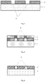
- FIGS. 3 to 6 show main process steps of a method for manufacturing a flat liquid crystal display device film according to one embodiment of the present disclosure, and during the process, a negative photoresist protection layer is not formed on a surface of a negative photoresist layer, in which:
- FIG. 3 schematically shows a step of exposing the negative photoresist layer which covers a substrate
- FIG. 4 schematically shows a structure of the negative photoresist layer with a space having a shape defined by a liquid crystal display device film
- FIG. 5 schematically shows a structure of embedding a positive photeresist layer after developing procedure in the space having the shape defined by the liquid crystal display device film of the liquid crystal display device film;
- FIG. 6 schematically shows a structure of obtained flat liquid crystal display device film
- FIGS. 3, 4, 7, and 8 show main process steps of a method for manufacturing a flat liquid crystal display device film according to the other embodiment of the present disclosure, and during the process, a negative photoresist protection layer is formed on a surface of a negative photoresist layer, in which:
- FIG. 7 schematically shows a structure of embedding a positive photeresist layer after developing procedure in the space having the shape defined by the liquid crystal display device film of the liquid crystal film display device;
- FIG. 8 schematically shows a structure of obtained flat liquid crystal display device film.
- a method of decreasing an RC delay by increasing a thickness of a metal layer will easily cause the problems such as corrosion of wiring and short connection, and a qualified rate of a product will be seriously reduced.
- there is no planarization technology in a traditional array manufacturing procedure which prevents continuous thickening of the metal layer, and limits continuous decrease of a signal line resistance.
- a negative photoresist is used to increase a flatness of an array, and to reduce influence of a wiring thickness on array topography, thereby realizing low resistance wiring. The present disclosure is based on the aforesaid method.
- FIGS. 3 to 6 show main process steps of a method for manufacturing a flat liquid crystal display device film according to the present embodiment.
- the flat liquid crystal display device film is made of one selected from a group consisting of metal M1 metal M2 and black matrix (BM).
- the method mainly comprises following steps.
- step A as shown in FIG. 3 , a negative photoresist layer 2 is coated on a substrate 1 , and the negative photoresist layer 2 is exposed with a liquid crystal display device film mask 6 to obtain a negative photoresist layer 2 after exposing procedure which covers the substrate 1 .
- step B the negative photoresist layer 2 after exposing procedure is developed, and a space 5 having a shape defined by a liquid crystal display device film is formed in a negative photoresist layer 2 ′ after developing procedure which covers an upper surface of the substrate. A structure thereof is shown in FIG. 4 .
- the structure comprises:
- the substrate 1 which is a glass substrate or a plastic substrate.
- the negative photoresist layer 2 ′ after developing procedure which is located on the upper surface of the substrate 1 .
- step D a liquid crystal display device film 3 is sputtered and grown on a surface of the negative photoresist layer 2 ′ after developing procedure and a surface of the space 5 having the shape defined by the liquid crystal display device film, so that the liquid crystal display device film 3 covers the surface of the negative photoresist layer 2 ′ after developing procedure, and meanwhile covers the surface of the space 5 having the shape defined by the liquid crystal display device film.
- a positive photoresist layer (a structure thereof is not shown in FIG. 5 ) is coated on a surface of the liquid crystal display device film 3 , so that the positive photoresist layer covers a surface of the liquid crystal display device film 3 , and fills the space 5 having the shape defined by the liquid crystal display film.
- step F the positive photeresist layer is exposed with a liquid crystal display device film mask 6 and developed to obtain a positive photoresist layer 4 ′ after developing procedure which is embedded in the space having the shape defined by the liquid crystal display device film of the liquid crystal display device film, and a structure thereof is shown in FIG. 5 .
- the structure comprises:
- the substrate 1 which is a glass substrate or a plastic substrate;
- the negative photoresist layer 2 ′ after developing procedure, which is located on the upper surface of the substrate 1 ;
- the liquid crystal display device film 3 which covers the surface of the negative photoresist layer 2 ′ after developing procedure, and meanwhile covers the surface of the space 5 having the shape defined by the liquid crystal display device film;
- the positive photoresist layer 4 ′ after developing procedure, which is embedded in the space 5 having the shape defined by the liquid crystal display device film of the liquid crystal display device film.
- step G excess liquid crystal display device film is etched with a photoresist pattern mask to obtain a flat liquid crystal display device film 3 ′.
- the flat liquid crystal display device film 3 ′ is embedded in the space 5 having the shape defined by the liquid crystal display device film of the negative photoresist layer 2 ′ after developing procedure and is flush with the negative photoresist layer 2 ′ after developing procedure. A structure thereof is shown in FIG. 6 .
- the structure comprises:
- the substrate 1 which is a glass substrate or a plastic substrate;
- the flat liquid crystal display device film 3 ′ which is embedded in the space 5 having the shape defined by the liquid crystal display device film of the negative photoresist layer after developing procedure.
- FIGS. 3, 4, 7, and 8 show main process steps of a method for manufacturing a flat liquid crystal display device film according to the present embodiment.
- the liquid crystal device film is made of one selected from a group consisting of metal M1, metal M2, and black matrix (BM).
- the method mainly comprises following steps.
- step A as shown in FIG. 3 , a negative photoresist layer 2 is coated on a substrate 1 , and the negative photoresist layer is exposed with a liquid crystal display device film mask 6 to obtain a negative photoresist layer 2 after exposing procedure which covers the substrate 1 .
- step B the negative photoresist layer 2 after exposing procedure is developed, and a space 5 having a shape defined by a liquid crystal display device film is formed in a negative photoresist layer 2 ′ after developing procedure which covers an upper surface of the substrate. A structure thereof is shown in FIG. 4 .
- the structure comprises:
- the substrate 1 which is a glass substrate or a plastic substrate.
- the negative photoresist layer 2 ′ after developing procedure which is located on the upper surface of the substrate 1 .
- a negative photoresist protection layer 7 is coated on a surface of the negative photoresist layer 2 ′ after developing procedure and a surface of the space 5 having the shape defined by the liquid crystal display device film.
- the negative photoresist protection layer 7 is preferably made of silicon nitride or silicon oxide.
- a thickness of the negative photoresist protection layer 7 is preferably in a range from 0.1 to 0.2 ⁇ m.
- step D the liquid crystal display device film 3 is sputtered and grown on a surface of the negative photoresist layer 2 ′ after developing procedure and a surface of the space 5 having the shape defined by the liquid crystal display device film which are both covered with a negative photoresist protection layer 7 , so that the liquid crystal display device film 3 covers the surface of the negative photoresist layer 2 ′ after developing procedure and the surface of the space 5 having the shape defined by the liquid crystal display device film which are both covered with a negative photoresist protection layer 7 . That is, the liquid crystal display device film 3 covers a surface of the negative photoresist protection layer 7 .
- a positive photoresist layer (a structure thereof is not shown herein) is coated on a surface of the liquid crystal display device film 3 , so that the positive photoresist layer covers a surface of the liquid crystal display device film 3 , and fills the space 5 having the shape defined by the liquid crystal display film.
- step F the positive photeresist layer is exposed with a liquid crystal display device film mask 6 and developed to obtain a positive photoresist layer 4 ′ after developing procedure which is embedded in the space having the shape defined by the liquid crystal display device film of the liquid crystal film, and a structure thereof is shown in FIG. 7 .
- the structure comprises:
- the substrate 1 which is a glass substrate or a plastic substrate;
- the negative photoresist layer 2 ′ after developing procedure, which is located on the upper surface of the substrate 1 ;
- the negative photoresist protection layer 7 which covers the surface of the negative photoresist layer 2 ′ after developing procedure and the surface of the space 5 having the shape defined by the liquid crystal display device film;
- liquid crystal display device film 3 which covers the surface of the negative photoresist protection layer 7 ;
- the positive photoresist layer 4 ′ after developing procedure, which is embedded in the space having the shape defined by the liquid crystal display device film of the liquid crystal display device film.
- step G excess liquid crystal display device film is etched with a photoresist pattern mask to obtain a flat liquid crystal display device film 3 ′.
- the flat liquid crystal display device film 3 ′ is embedded in the space 5 having the shape defined by the liquid crystal display device film of the negative photoresist layer 2 ′ after developing procedure and is flush with the negative photoresist layer 2 ′ after developing procedure. A structure thereof is shown in FIG. 8 .
- the structure comprises:
- the substrate 1 which is a glass substrate or a plastic substrate;
- the negative photoresist layer 2 ′ after developing procedure, which is located on an upper surface of the substrate 1 ;
- the negative photoresist protection layer 7 which covers the surface of the negative photoresist layer 2 ′ after developing procedure and the surface of the space 5 having the shape defined by the liquid crystal display device film;
- the flat liquid crystal display device film 3 ′ which is embedded in the space 5 having the shape defined by the liquid crystal display device film of the negative photoresist layer after developing procedure which is covered with the negative photoresist protection layer 7 .
- the negative photoresist protection layer is not formed on the surface of the negative photoresist layer. Therefore, when the negative photoresist layer after exposing procedure is developed, a developer used therein should be selected carefully to prevent the negative photoresist layer from being damaged.
- the negative photoresist protection layer is formed on the surface of the negative photoresist layer. Therefore, when the negative photoresist layer after exposing procedure is developed, the developer used therein can be selected from a wide range.
- influence of a wiring thickness on topography of array film can be reduced. Without affecting a qualified rate of a product, a low-resistance wiring can be realized, and thus an RC delay during signal transmission of a large-sized panel can be reduced. Meanwhile, when the method is applied, a metal layer with a larger thickness relative to that of a metal layer made by a conventional method can be made. Therefore, wiring load of a large-sized panel can be reduced, resistance of signal line can be reduced, RC delay can be decreased, and display quality can be improved.
Abstract
Description
Claims (8)
Applications Claiming Priority (4)
| Application Number | Priority Date | Filing Date | Title |
|---|---|---|---|
| CN201611244077 | 2016-12-29 | ||
| CN201611244077.9A CN106773171B (en) | 2016-12-29 | 2016-12-29 | A method of preparing planarization liquid crystal display film layer |
| CN201611244077.9 | 2016-12-29 | ||
| PCT/CN2017/071236 WO2018120317A1 (en) | 2016-12-29 | 2017-01-16 | Method for manufacturing planarized liquid crystal display film layer |
Publications (2)
| Publication Number | Publication Date |
|---|---|
| US20180341131A1 US20180341131A1 (en) | 2018-11-29 |
| US10656446B2 true US10656446B2 (en) | 2020-05-19 |
Family
ID=58928677
Family Applications (1)
| Application Number | Title | Priority Date | Filing Date |
|---|---|---|---|
| US15/329,372 Active 2037-05-21 US10656446B2 (en) | 2016-12-29 | 2017-01-16 | Method for manufacturing flat liquid crystal display device film |
Country Status (3)
| Country | Link |
|---|---|
| US (1) | US10656446B2 (en) |
| CN (1) | CN106773171B (en) |
| WO (1) | WO2018120317A1 (en) |
Citations (8)
| Publication number | Priority date | Publication date | Assignee | Title |
|---|---|---|---|---|
| JP2000298208A (en) * | 1999-04-13 | 2000-10-24 | Toppan Printing Co Ltd | Color filter and production thereof, and el display and liquid crystal display using the same |
| US20090226629A1 (en) * | 2008-03-06 | 2009-09-10 | Taiwan Tft Lcd Association | Method for fabricating display substrate and liquid crystal display |
| CN102394238A (en) | 2011-06-16 | 2012-03-28 | 友达光电股份有限公司 | Manufacturing procedure of electric conduction structure |
| US20130093971A1 (en) | 2011-10-12 | 2013-04-18 | Sony Corporation | Liquid crystal device and electronic apparatus |
| CN103700674A (en) | 2013-12-27 | 2014-04-02 | 京东方科技集团股份有限公司 | Array substrate, preparation method thereof and display device |
| CN103779202A (en) | 2014-01-27 | 2014-05-07 | 深圳市华星光电技术有限公司 | Pixel structure, manufacturing method thereof and display panel |
| CN104460093A (en) | 2014-12-31 | 2015-03-25 | 深圳市华星光电技术有限公司 | Thin film transistor array substrate, manufacturing method thereof and displaying device |
| CN104698709A (en) | 2015-04-01 | 2015-06-10 | 上海天马微电子有限公司 | Array substrate and liquid crystal display panel |
-
2016
- 2016-12-29 CN CN201611244077.9A patent/CN106773171B/en active Active
-
2017
- 2017-01-16 US US15/329,372 patent/US10656446B2/en active Active
- 2017-01-16 WO PCT/CN2017/071236 patent/WO2018120317A1/en active Application Filing
Patent Citations (8)
| Publication number | Priority date | Publication date | Assignee | Title |
|---|---|---|---|---|
| JP2000298208A (en) * | 1999-04-13 | 2000-10-24 | Toppan Printing Co Ltd | Color filter and production thereof, and el display and liquid crystal display using the same |
| US20090226629A1 (en) * | 2008-03-06 | 2009-09-10 | Taiwan Tft Lcd Association | Method for fabricating display substrate and liquid crystal display |
| CN102394238A (en) | 2011-06-16 | 2012-03-28 | 友达光电股份有限公司 | Manufacturing procedure of electric conduction structure |
| US20130093971A1 (en) | 2011-10-12 | 2013-04-18 | Sony Corporation | Liquid crystal device and electronic apparatus |
| CN103700674A (en) | 2013-12-27 | 2014-04-02 | 京东方科技集团股份有限公司 | Array substrate, preparation method thereof and display device |
| CN103779202A (en) | 2014-01-27 | 2014-05-07 | 深圳市华星光电技术有限公司 | Pixel structure, manufacturing method thereof and display panel |
| CN104460093A (en) | 2014-12-31 | 2015-03-25 | 深圳市华星光电技术有限公司 | Thin film transistor array substrate, manufacturing method thereof and displaying device |
| CN104698709A (en) | 2015-04-01 | 2015-06-10 | 上海天马微电子有限公司 | Array substrate and liquid crystal display panel |
Non-Patent Citations (3)
| Title |
|---|
| Chinese Office Action dated Feb. 12, 2018 for Chinese Patent Application No. 201611244077.9. |
| Computer-generated translation of JP 2000-298208 (Year: 2000). * |
| International Search Report dated Jan. 16, 2017 for International Patent Application No. PCT/CN2017/071236. |
Also Published As
| Publication number | Publication date |
|---|---|
| US20180341131A1 (en) | 2018-11-29 |
| CN106773171A (en) | 2017-05-31 |
| CN106773171B (en) | 2018-09-25 |
| WO2018120317A1 (en) | 2018-07-05 |
Similar Documents
| Publication | Publication Date | Title |
|---|---|---|
| US9958747B2 (en) | Array substrate and manufacturing method thereof, display panel and display device | |
| WO2018176760A1 (en) | Flexible display panel, display device, and method for manufacturing flexible display panel | |
| CN101825815B (en) | TFT (Thin Film Transistor)-LCD (Liquid Crystal Display) array baseplate and manufacturing method thereof | |
| US20160306220A1 (en) | A color filter on array substrate and fabricating method thereof as well as a display device | |
| CN104749816A (en) | Manufacturing method of display substrate, display substrate and display device | |
| US10209584B2 (en) | Manufacturing method of metal layer, functional substrate and manufacturing method thereof, and display device | |
| US9905593B2 (en) | Mask plate and method for manufacturing array substrate | |
| WO2019100502A1 (en) | Thin film transistor liquid crystal display array substrate and manufacturing method therefor | |
| WO2014205998A1 (en) | Coa substrate and manufacturing method therefor, and display device | |
| US7678619B2 (en) | Method of manufacturing a thin film transistor matrix substrate | |
| WO2016112684A1 (en) | Display panel and manufacturing method therefor, and display device | |
| US20120113366A1 (en) | Array substrate and liquid crystal display | |
| WO2020133651A1 (en) | Pixel electrode structure and manufacturing method therefor | |
| US9791755B2 (en) | Color filter-on-array substrate, display device, and method for manufacturing the color filter-on-array substrate | |
| WO2017185877A1 (en) | Array substrate and manufacturing method therefor | |
| WO2018157573A1 (en) | Gate electrode structure and manufacturing method therefor, and display device | |
| WO2016106876A1 (en) | Thin-film transistor array substrate, manufacturing method therefor, and display device | |
| EP3657241B1 (en) | Array substrate and manufacturing method thereof, and display device | |
| WO2016155429A1 (en) | Display substrate and manufacturing method therefor, and display device | |
| WO2019218822A1 (en) | Thin-film transistor and manufacturing method therefor, array substrate, and display device | |
| JP2006276327A (en) | Liquid crystal display device and manufacturing method thereof | |
| US20120241746A1 (en) | Electrophoresis display and manufacturing method | |
| US10942403B2 (en) | Display substrate and display apparatus | |
| JP2013080159A (en) | Liquid crystal display device and method for manufacturing the same | |
| US10656446B2 (en) | Method for manufacturing flat liquid crystal display device film |
Legal Events
| Date | Code | Title | Description |
|---|---|---|---|
| AS | Assignment |
Owner name: SHENZHEN CHINA STAR OPTOELECTRONICS TECHNOLOGY CO., LTD., CHINA Free format text: ASSIGNMENT OF ASSIGNORS INTEREST;ASSIGNORS:YUE, SHOUZHEN;ZHANG, MENGMENG;REEL/FRAME:044049/0067 Effective date: 20170405 Owner name: SHENZHEN CHINA STAR OPTOELECTRONICS TECHNOLOGY CO. Free format text: ASSIGNMENT OF ASSIGNORS INTEREST;ASSIGNORS:YUE, SHOUZHEN;ZHANG, MENGMENG;REEL/FRAME:044049/0067 Effective date: 20170405 |
|
| STPP | Information on status: patent application and granting procedure in general |
Free format text: DOCKETED NEW CASE - READY FOR EXAMINATION |
|
| STPP | Information on status: patent application and granting procedure in general |
Free format text: NON FINAL ACTION MAILED |
|
| STPP | Information on status: patent application and granting procedure in general |
Free format text: RESPONSE TO NON-FINAL OFFICE ACTION ENTERED AND FORWARDED TO EXAMINER |
|
| STPP | Information on status: patent application and granting procedure in general |
Free format text: NOTICE OF ALLOWANCE MAILED -- APPLICATION RECEIVED IN OFFICE OF PUBLICATIONS |
|
| STPP | Information on status: patent application and granting procedure in general |
Free format text: PUBLICATIONS -- ISSUE FEE PAYMENT VERIFIED |
|
| STCF | Information on status: patent grant |
Free format text: PATENTED CASE |
|
| FEPP | Fee payment procedure |
Free format text: MAINTENANCE FEE REMINDER MAILED (ORIGINAL EVENT CODE: REM.); ENTITY STATUS OF PATENT OWNER: LARGE ENTITY |