US10649000B2 - Connection assembly - Google Patents
Connection assembly Download PDFInfo
- Publication number
- US10649000B2 US10649000B2 US15/760,615 US201615760615A US10649000B2 US 10649000 B2 US10649000 B2 US 10649000B2 US 201615760615 A US201615760615 A US 201615760615A US 10649000 B2 US10649000 B2 US 10649000B2
- Authority
- US
- United States
- Prior art keywords
- sensor
- axis
- acceleration
- substrate
- electrode
- Prior art date
- Legal status (The legal status is an assumption and is not a legal conclusion. Google has not performed a legal analysis and makes no representation as to the accuracy of the status listed.)
- Active, expires
Links
Images


Classifications
-
- G—PHYSICS
- G01—MEASURING; TESTING
- G01P—MEASURING LINEAR OR ANGULAR SPEED, ACCELERATION, DECELERATION, OR SHOCK; INDICATING PRESENCE, ABSENCE, OR DIRECTION, OF MOVEMENT
- G01P15/00—Measuring acceleration; Measuring deceleration; Measuring shock, i.e. sudden change of acceleration
- G01P15/02—Measuring acceleration; Measuring deceleration; Measuring shock, i.e. sudden change of acceleration by making use of inertia forces using solid seismic masses
- G01P15/08—Measuring acceleration; Measuring deceleration; Measuring shock, i.e. sudden change of acceleration by making use of inertia forces using solid seismic masses with conversion into electric or magnetic values
- G01P15/125—Measuring acceleration; Measuring deceleration; Measuring shock, i.e. sudden change of acceleration by making use of inertia forces using solid seismic masses with conversion into electric or magnetic values by capacitive pick-up
-
- G—PHYSICS
- G01—MEASURING; TESTING
- G01P—MEASURING LINEAR OR ANGULAR SPEED, ACCELERATION, DECELERATION, OR SHOCK; INDICATING PRESENCE, ABSENCE, OR DIRECTION, OF MOVEMENT
- G01P15/00—Measuring acceleration; Measuring deceleration; Measuring shock, i.e. sudden change of acceleration
- G01P15/02—Measuring acceleration; Measuring deceleration; Measuring shock, i.e. sudden change of acceleration by making use of inertia forces using solid seismic masses
- G01P15/08—Measuring acceleration; Measuring deceleration; Measuring shock, i.e. sudden change of acceleration by making use of inertia forces using solid seismic masses with conversion into electric or magnetic values
- G01P15/0802—Details
-
- G—PHYSICS
- G01—MEASURING; TESTING
- G01P—MEASURING LINEAR OR ANGULAR SPEED, ACCELERATION, DECELERATION, OR SHOCK; INDICATING PRESENCE, ABSENCE, OR DIRECTION, OF MOVEMENT
- G01P15/00—Measuring acceleration; Measuring deceleration; Measuring shock, i.e. sudden change of acceleration
- G01P15/18—Measuring acceleration; Measuring deceleration; Measuring shock, i.e. sudden change of acceleration in two or more dimensions
-
- H01L29/84—
-
- H—ELECTRICITY
- H10—SEMICONDUCTOR DEVICES; ELECTRIC SOLID-STATE DEVICES NOT OTHERWISE PROVIDED FOR
- H10D—INORGANIC ELECTRIC SEMICONDUCTOR DEVICES
- H10D48/00—Individual devices not covered by groups H10D1/00 - H10D44/00
- H10D48/50—Devices controlled by mechanical forces, e.g. pressure
-
- G—PHYSICS
- G01—MEASURING; TESTING
- G01P—MEASURING LINEAR OR ANGULAR SPEED, ACCELERATION, DECELERATION, OR SHOCK; INDICATING PRESENCE, ABSENCE, OR DIRECTION, OF MOVEMENT
- G01P15/00—Measuring acceleration; Measuring deceleration; Measuring shock, i.e. sudden change of acceleration
- G01P15/02—Measuring acceleration; Measuring deceleration; Measuring shock, i.e. sudden change of acceleration by making use of inertia forces using solid seismic masses
- G01P15/08—Measuring acceleration; Measuring deceleration; Measuring shock, i.e. sudden change of acceleration by making use of inertia forces using solid seismic masses with conversion into electric or magnetic values
- G01P2015/0862—Measuring acceleration; Measuring deceleration; Measuring shock, i.e. sudden change of acceleration by making use of inertia forces using solid seismic masses with conversion into electric or magnetic values being provided with particular means being integrated into a MEMS accelerometer structure for providing particular additional functionalities to those of a spring mass system
Definitions
- the present invention relates to a connection assembly applicable to various sensors, such as an acceleration sensor.
- connection assemblies 1 to 3 disclose connection assemblies each providing an electrical connection between a wiring and a semiconductor substrate with the wiring between the semiconductor substrate and a glass substrate.
- PTLs 2, 4, and 5, for example, disclose conventional sensors having structures including a silicon substrate and glass substrates which are stacked. In these sensors, anodic bonding for stacking the silicon substrate and the glass substrates may cause warpage in these substrates. This may reduce accuracy of these sensors.
- MEMS sensors have been known (see PYLs 1 to 3, for example). These sensors can detect acceleration of a mass body such that the sensors detect a displacement of the mass body by sensing a change in capacitance between a fixed electrode and an electrode disposed on the mass body, and then, determine the acceleration based on the detected displacement of the mass body.
- MEMS sensors which can detect acceleration with sensors having comb shapes are disclosed in, for example, PTLs 1 to 3.
- MEMS sensors are disclosed in 'TLs 7 and 8, each of which is provided with a correction circuit to correct its sensitivity in a direction in a main axis by using an output in a direction of another axis.
- a connection assembly includes a sensor substrate, a layer substrate coupled to the sensor substrate so as to face an upper surface of the sensor substrate, and a wire connected between the sensor substrate and the layer substrate.
- the sensor substrate includes first and second projections provide on the upper surface of the sensor substrate and extending in an extension direction along the upper surface of the sensor substrate.
- the wire has a first end sandwiched between the layer substrate and the first projection, and a second end sandwiched between the layer substrate and the second projection.
- connection assembly provides reliable connection.
- FIG. 1 is an exploded perspective view of a sensor according to Exemplary Embodiment 1.
- FIG. 2 is a cross-sectional view of the sensor according to Embodiment 1.
- FIG. 3 is an exploded perspective view of a sensor chip of the sensor according to Embodiment 1.
- FIG. 4 is a top perspective view of a sensor substrate of the sensor chip according to Embodiment 1.
- FIG. 5 is a top perspective view of the sensor substrate of the sensor chip according to Embodiment 1.
- FIG. 6 is a bottom perspective view of the sensor substrate of the sensor chip according to Embodiment 1.
- FIG. 7 is a bottom perspective view of the sensor substrate of the sensor chip according to Embodiment 1.
- FIG. 8A is an enlarged view of the sensor shown in FIG. 5 .
- FIG. 8B is a cross-sectional view of the sensor on lines 8 B- 8 B shown in FIG. 8A .
- FIG. 9 is a top view of a sensor chip of a sensor according to Exemplary Embodiment 2.
- FIG. 10 is a top view of the sensor chip according to Embodiment 2.
- FIG. 11 is a top view of the sensor chip according to Embodiment 2.
- FIG. 12 is a top view of the sensor chip according to Embodiment 2.
- FIG. 13 is an enlarged view of a sensor according to Exemplary Embodiment 4.
- FIG. 14 is an enlarged view of the sensor shown in FIG. 13 .
- FIG. 15 is a perspective view of a sensor according to Exemplary Embodiment 5.
- FIG. 16 is an exploded perspective view of a sensor chip of the sensor according to Embodiment 5.
- FIG. 17A is a cross-sectional view of an X-detection part of the sensor chip according to Embodiment 5.
- FIG. 17B is a cross-sectional view of a Z-detection part of the sensor chip according to Embodiment 5.
- FIG. 18 is a cross-sectional view of the X-detection part having no acceleration in an X-direction applied thereto.
- FIG. 19 is a circuit diagram of the X-detection part shown in FIG. 18 .
- FIG. 20 is a cross-sectional view of the X-detection part having an acceleration in the X-direction applied thereto.
- FIG. 21 is a circuit diagram of the X-detection part shown in FIG. 20 .
- FIG. 22 is a cross-sectional view of a Z-detection part having an acceleration in a Z-direction applied thereto.
- FIG. 23 is a circuit diagram of the Z-detection part shown in FIG. 22 .
- FIG. 24A illustrates an output of the sensor according to Embodiment 5 that indicates acceleration in a direction of a main axis.
- FIG. 24B illustrates an output of the sensor according to Embodiment 5 that indicates acceleration in a direction of another axis.
- FIG. 24C is a schematic cross-sectional view of the X-detection part of the sensor according to Embodiment 5.
- FIG. 25A illustrates output characteristics of the sensor according to Embodiment 5 that indicate acceleration in the direction of the main axis.
- FIG. 25B illustrates output characteristics of the sensor according to Embodiment 5 that indicate acceleration in the direction of another axis.
- FIG. 25C is a schematic cross-sectional view of the X-detection part of the sensor according to Embodiment 5.
- FIG. 26 is a functional block diagram of the sensor according to Embodiment 5.
- FIG. 27 illustrates an output of the X-detection part of the sensor according to Embodiment 5.
- FIG. 28A illustrates an output that is obtained by correcting an output of an X-detection part with a correction circuit of a sensor of a comparative example.
- FIG. 28B illustrates an output obtained by correcting the output of the X-detection part with the correction circuit of the sensor of the comparative example.
- FIG. 29A illustrates an output obtained by correcting an output of the X-detection part with another correction circuit of the sensor according to the embodiment.
- FIG. 29B illustrates output obtained by correcting the output of the X-detection part with the correction circuit shown in FIG. 29A .
- FIG. 1 is an exploded perspective view of sensor 701 according to Exemplary Embodiment 1.
- Sensor 701 according to Embodiment 1 is an acceleration sensor for detecting an acceleration applied thereto.
- Sensor 701 includes sensor chip 4100 , integrated circuit 4200 performing various calculations based on outputs from sensor chip 4100 , package 4300 accommodating therein sensor chip 4100 and integrated circuit 4200 , terminals 4400 led out from package 4300 , leads 4402 led out from package 4300 , and lid 4600 covering an upper surface of package 4300 .
- integrated circuit 4200 is an application-specific integrated circuit (ASIC).
- ASIC application-specific integrated circuit
- Integrated circuit 4200 is connected electrically to sensor chip 4100 via metal wires so as to process electrical signals, such as signals indicating acceleration, output from sensor chip 4100 . Then, the integrated circuit outputs the processed signal to the outside of package 4300 .
- Lid 4600 is made of metal material, such as stainless steel, and is disposed at a position covering an opening of package 4300 . In other words, lid 4600 is disposed at the position to cover both sensor chip 4100 and integrated circuit 4200 .
- Package 4300 is made of resin material, such as liquid crystal polymer.
- Each of side surfaces of package 4300 facing leads 4402 inclines toward the inside of the package such that positions on the side surfaces located more inside as the positions approaches lid 4600 .
- the term “inside” here means “a side in which integrated circuit 4200 and sensor chip 4100 are accommodated.” This configuration provides a large space between package 4300 and each of leads 4402 . Such a large space allows leads 4402 to be bent easily and does not prevent leads 4402 from functioning as spring.
- Package 4300 accommodates both sensor chip 4100 and integrated circuit 4200 in the inside of the package. Both terminals 4400 and leads 4402 extend out from package 4300 .
- Terminals 4400 are electrically connected to a board outside sensor 701 .
- Leads 4402 are electrically connected to lid 4600 .
- FIG. 2 is a cross-sectional view of sensor 701 .
- Each of leads 4402 includes part 4402 a and part 4402 b connected to part 4402 a .
- Part 4402 a extends out from package 4300 and extends further along the side surface of package 4300 . While FIG. 2 illustrates part 4402 a extending in a vertical direction, the configuration is not limited to the case; the part, for example, may extend along the inward inclination of the side surface of package 4300 .
- Part 4402 a is electrically connected to ground 4404 . This configuration reduces a potential of lid 4600 connected with part 4402 b to a ground potential.
- Part 4402 b extends toward the inside of package 4300 , and is sandwiched between lid 4600 and package 4300 to be electrically connected to lid 4600 .
- part 4402 b which is a distal end of lead 4402 having been bent is pushed against lid 4600 by a spring force of lead 4402 per se.
- This configuration allows part 4402 b to be electrically connected to lid 4600 stably.
- Part 4402 b is disposed in recess 4300 p provided in an upper edge of package 4300 .
- the depth of recess 4300 p is preferably larger than the thickness of part 4402 b .
- This configuration provides space 4302 between package 4300 and lid 4600 after lid 4600 is attached. In this configuration, for example, an X-ray inspection from a lateral direction can simply be performed to confirm whether or not leads 4402 appropriately contact lid 4600 .
- the depth of recess 4300 p may be not larger than the thickness of part 4402 b .
- the depth of recess 4300 p may be substantially equal to the thickness of part 4402 b .
- the upper edge of package 4300 can be approximately flush with part 4402 b , hence reducing the size of package 4300 .
- End 4402 c of part 4402 b protrudes inward from inner wall surface 4300 t of package 4300 which extends along line L.
- an X-ray inspection from above can be simply performed to confirm whether or not leads 4402 are appropriately disposed.
- Plural terminals 4400 configure to be connected to an external board extend from package 4300 .
- FIG. 3 is an exploded perspective view of sensor chip 4100 .
- Sensor chip 4100 is a connection assembly that includes: sensor substrate 401 , layer substrate 402 a joined to sensor substrate 401 , and layer substrate 402 b joined to sensor substrate 401 .
- Layer substrate 402 a is located above sensor substrate 401 while layer substrate 402 b is located below sensor substrate 401 .
- Sensor substrate 401 is sandwiched between layer substrates 402 a and 402 b .
- Sensor substrate 401 is made of, e.g. a silicon-on-insulator (SOI) substrate.
- Layer substrates 402 a and 402 b are made of insulator, such as glass. In other words, layer substrate 402 a is a glass substrate, and layer substrate 402 b is a glass substrate.
- SOI silicon-on-insulator
- Sensor chip 4100 includes X-detection part 410 detecting acceleration in a direction of the X-axis, Y-detection part 420 detecting acceleration in a direction of the Y-axis, and Z-detection part 430 detecting acceleration in a direction of the Z-axis.
- the X-axis is contained in an XY-plane.
- the Y-axis is contained in the XY-plane and perpendicular to the X-axis.
- the Z-axis is perpendicular to the XY-plane.
- X-detection part 410 includes rectangular frame 410 a , beams 412 a and 412 b connected to rectangular frame 410 a , movable electrode 411 supported by beams 412 a and 412 b , and fixed electrodes 413 a and 413 b .
- Beams 412 a and 412 b are arranged on axis A 410 parallel to the Y-axis, and are disposed at position opposite to each other with respect to movable electrode 411 .
- Movable electrode 411 is coupled to and supported by rectangular frame 410 a via beams 412 a and 412 b .
- Movable electrode 411 can swing about axis A 410 , thereby detecting an acceleration in a direction of the X-axis.
- Axis A 410 divides an upper surface of movable electrode 411 into two parts. One of the two parts of the upper surface of movable electrode 411 faces fixed electrode 413 a in a direction of the Z-axis with a space between the part and fixed electrode 413 a while the other part faces fixed electrode 413 b in the direction of the Z-axis with a space between the part and fixed electrode 413 b .
- Acceleration in a direction of the X-axis can be detected based on changes in a capacitance between movable electrode 411 and fixed electrode 413 a and a capacitance between movable electrode 411 and fixed electrode 413 b.
- Y-detection part 420 includes rectangular frame 420 a , beams 422 a and 422 b connected to rectangular frame 420 a , movable electrode 421 supported by beams 422 a and 422 b , and fixed electrodes 423 a and 423 b .
- Beams 422 a and 422 b are arranged on axis A 420 parallel to the X-axis, and are disposed opposite to each other with respect to movable electrode 421 .
- Movable electrode 421 is coupled to and supported by rectangular frame 420 a via beams 422 a and 422 b .
- Movable electrode 421 can swing about axis A 420 , thereby detecting acceleration in a direction of the Y-axis.
- Axis A 420 divides an upper surface of movable electrode 421 into two parts.
- One part of the two parts the upper surface of movable electrode 421 faces fixed electrode 423 a in the direction of the Z-axis with a space between the part and fixed electrode 423 a .
- the other part of the two parts of the upper surface of movable electrode 421 faces fixed electrode 423 b in the direction of the Z-axis with a space between the part and fixed electrode 423 b .
- Acceleration in a direction of the Y-axis can be detected based on changes in a capacitance between movable electrode 421 and fixed electrode 423 a and a capacitance between movable electrode 421 and fixed electrode 423 b.
- Z-detection part 430 includes rectangular frame 430 a , beams 432 a , 432 b , 432 c , and 432 d connected to rectangular frame 430 a , movable electrode 431 supported by beams 432 a , 432 b , 432 c , and 432 d , and fixed electrodes 433 a and 433 b .
- Movable electrode 431 is coupled to and supported by rectangular frame 430 a via beams 432 a , 432 b , 432 c , and 432 d .
- Movable electrode 431 supported by beams 432 a , 432 b , 432 c , and 432 d can be translated in a direction of the Z-axis, thereby detecting acceleration in a direction of the Z-axis.
- An upper surface of movable electrode 431 faces fixed electrode 433 a in the direction of the Z-axis with a space between movable electrode 431 and fixed electrode 433 a .
- a lower surface of movable electrode 431 faces fixed electrode 433 b in the direction of the Z-axis with a space between movable electrode 431 and fixed electrode 433 b .
- Acceleration in the direction of the Z-axis can be detected based on changes in capacitance between movable electrode 431 and fixed electrode 433 a and a capacitance between movable electrode 431 and fixed electrode 433 b.
- X-detection part 410 and Y-detection part 420 have the same shape, and are disposed with each turning on itself by 90 degrees relative to one another.
- Z-detection part 430 is disposed between X-detection part 410 and Y-detection part 420 .
- X-detection part 410 , Y-detection part 420 , and Z-detection part 430 are disposed in a single chip. That is, as shown in FIG. 3 , rectangular frames 410 a , 420 a , and 430 a are arranged on a line extending in a direction of the Y-axis.
- Movable electrode 411 is disposed inside rectangular frame 410 a .
- Movable electrode 421 is disposed inside rectangular frame 420 a .
- Movable electrode 431 is disposed inside rectangular frame 430 a .
- Movable electrode 411 , movable electrode 421 , and movable electrode 431 have substantially rectangular shapes viewing from above.
- a clearance of a predetermined width is provided between movable electrode 411 and a side wall of rectangular frame 410 a .
- a clearance of a predetermined width is provided between movable electrode 421 and a side wall of rectangular frame 420 a .
- a clearance of a predetermined width is provided between movable electrode 431 and a side wall of rectangular frame 430 a .
- the shape of frames 410 a , 420 a , and 430 a is not necessarily the rectangular shape, and may be other shapes, such as a circular shape.
- Sensor substrate 401 is joined to layer substrate 402 a at connection part 403 .
- Via-electrodes 414 a and 414 b are made of conductive material, such as silicon, tungsten, or copper. Parts surrounding and holding via-electrodes 414 a and 414 b are made of insulating material, such as glass.
- each beams 412 a and 412 b couples respective one of substantial centers of the two opposite sides of a surface of movable electrode 411 to respective one of side walls of rectangular frame 410 a , thereby swingably supporting movable electrode 411 .
- Fixed electrodes 413 a and 413 b are disposed on a side of layer substrate 402 a which faces movable electrode 411 fixed electrodes 413 a and 413 b while the boundary line between fixed electrodes 413 a and 413 b is axis A 410 that connects between beam 412 a and beam 412 b .
- Via-electrodes 414 a and 414 b are made of conductive material, such as silicon, tungsten, or copper.
- a part surrounding and holding via-electrodes 414 a and 414 b is made of insulating material, such as glass.
- each of beams 422 a and 422 b couples respective one of substantial centers of the two opposite sides of a surface of movable electrode 421 to respective one of side walls of rectangular frame 420 a , thereby swingably supporting movable electrode 421 .
- Fixed electrodes 423 a and 423 b are provided on a side of layer substrate 402 a which faces movable electrode 421 while the boundary line between fixed electrodes 423 a and 423 b is axis A 420 that connects between beam 422 a and beam 422 b .
- Via-electrodes 424 a and 424 b are made of conductive material, such as silicon, tungsten, or copper.
- a part surrounding and holding via-electrodes 424 a and 424 b is made of insulating material, such as glass.
- Z-detection part 430 four corners of movable electrode 431 are coupled to the side walls of rectangular frame 430 a via two pair pf beams 432 a , 432 b , 432 c , and 432 d having L-shapes.
- This configuration allows movable electrode 431 to be translated in parallel with the Z-axis.
- the shape of beams 432 a , 432 b , 432 c , and 432 d is not necessarily the L-shape.
- the L-shape provides beams 432 a , 432 b , 432 c , and 432 d with a large length.
- Fixed electrode 433 a facing movable electrode 431 is disposed on a lower surface of layer substrate 402 a .
- Fixed electrode 433 b facing movable electrode 431 is disposed on the upper surface of layer substrate 402 b .
- Fixed electrode 433 a is led out to the upper surface of layer substrate 402 a through via-electrode 434 a .
- Fixed electrode 433 b is coupled to columnar electrode 435 b that is separated away from movable electrode 431 while columnar electrode 435 b is coupled to via-electrode 434 b that is disposed in layer substrate 402 a .
- Via-electrodes 434 a and 434 b are made of conductive material, such as silicon, tungsten, or copper.
- Parts of layer substrate 402 a and 402 b surrounding and holding via-electrodes 434 a and 434 b are made of insulating material, such as glass.
- FIGS. 4 and 5 are top perspective views of sensor substrate 401 .
- some of the electrodes are omitted for convenience of description.
- Each of columnar electrodes 435 a , 435 b , 435 c , and 435 d is electrically insulated from all the movable electrodes and all the beams.
- the columnar electrodes are formed by forming through-holes in a part of sensor substrate 401 .
- Columnar electrode 435 a is electrically connected to fixed electrode 433 a .
- Columnar electrode 435 b is electrically connected to fixed electrode 433 b.
- Sensor substrate 401 is joined to layer substrate 402 a at connection part 403 .
- Sensor substrate 401 includes connection parts 441 a and 441 b protruding toward layer substrate 402 a .
- Connection parts 441 a and 441 b are joined to layer substrate 402 a .
- Projections 442 a and 442 b are disposed close to connection part 441 a .
- connection part 441 a , projection 442 a , and projection 442 b are disposed at respective positions which lie on virtual straight line L 401 in parallel with the upper surface of sensor substrate 401 .
- Projection 442 c and projection 442 d are disposed close to projection 442 a and projection 442 b , respectively. The material, structure, size, positional relation of each of the projections will be described later.
- Sensor substrate 401 includes connection part 441 d protruding toward layer substrate 402 b .
- Connection part 441 d is joined to layer substrate 402 b similarly to connection part 441 b.
- Electrode 438 a is disposed at a position overlapping beams 432 a , 432 b , 432 c , and 432 d viewing from above. Electrodes 438 a is electrically connected to columnar electrode 435 c , columnar electrode 435 d , and via-electrode 434 b.
- Electrode 438 b is electrically connected to columnar electrode 435 b and via-electrode 434 b .
- a function of electrode 438 a will be described below.
- Sensor substrate 401 can be joined to layer substrates 402 a and 402 b by anodic bonding.
- the anodic bonding is a joining method in which sensor substrate 401 and layer substrate 402 a are heated while an electric voltage applied between sensor substrate 401 and each of layer substrates 402 a and 402 b .
- the applied electric voltage between sensor substrate 401 and layer substrate 402 a causes attraction between layer substrate 402 a and each of the movable electrodes.
- the electric potential of electrodes 438 a is substantially equal to the electric potential of sensor substrate 401 . This configuration prevents the movable electrodes from contacting layer substrate 402 a , thereby preventing failures, such as sticking.
- Columnar electrodes 435 a and 435 b are disposed at positions facing each other across movable electrode 431 sandwiched between columnar electrodes 435 a and 435 b .
- Columnar electrodes 435 c and 435 d are disposed at positions face each other across movable electrode 431 sandwiched between columnar electrodes 435 c and 435 d.
- FIGS. 6 and 7 are bottom views of sensor substrate 401 . In FIG. 6 , some of the electrodes are omitted for convenience of description.
- Electrode 438 c is disposed at a periphery of fixed electrode 433 b . Electrode 438 c is electrically connected to columnar electrodes 435 c and 435 d.
- Sensor substrate 401 includes connection parts 441 c and 441 d protruding toward layer substrate 402 b .
- Connection parts 441 c and 441 d are joined to layer substrate 402 b.
- FIG. 8A is an enlarged view of sensor substrate 401 shown in FIG. 5 .
- FIG. 8B is a cross-sectional view of sensor substrate 401 on line 8 B- 8 B shown in FIG. 8A .
- Projections 442 a , 442 b , 442 c , and 442 d are disposed on upper surface 1435 a of columnar electrode 435 a which is a part of the upper surface of sensor substrate 401 .
- Projections 442 c and 442 d are preferably made of the same member as columnar electrode 435 a , but may be made of different material.
- Projections 442 a and 442 b are made of metal that is disposed on the upper surfaces of oxide films 444 disposed on the upper surface of sensor substrate 401 . The heights of projections 442 a and 442 b can be adjusted by adjusting the thickness of oxide films 444 .
- Projections 442 a to 442 d extend slenderly along extension direction A 402 .
- Wire 439 a , wire 439 b , wire 439 c , and wire 439 d electrically connect between electrodes 438 c.
- Electrode 439 e includes a part forming a T-shape viewing from above.
- the part having the T-shape includes straight part 1439 e extending from edge part 439 e 1 to edge part 439 e 2 and straight part 2439 e extending perpendicularly from straight part 1439 e from a substantial midpoint of straight part 1439 e between edge part 439 e 1 and edge part 439 e 2 .
- Edge part 439 e 1 is sandwiched between layer substrate 402 a and projection 442 a while edge part 439 e 2 is sandwiched between layer substrate 402 a and projection 442 b.
- Wire 439 e and all the projections are sandwiched between layer substrate 402 a and sensor substrate 401 , thereby electrically connecting wire 439 e to the projections.
- Projections 442 c and 442 d extend in extension direction A 401 in parallel with projections 442 a and 442 b , and are arranged in direction A 401 perpendicular to extension direction A 402 .
- Straight part 1439 e of wire 439 e extends slenderly in extension direction A 401 .
- Straight part 2439 e extends slenderly in direction A 402 .
- the length of projection 442 c in extension direction A 402 is larger than the length of projection 442 a in extension direction A 402 .
- the length of projection 442 d in extension direction A 402 is larger than the length of projection 442 b in extension direction A 402 .
- the widths of projection 442 c in direction A 401 and projection 442 d are larger than the widths of projections 442 a and 442 b in direction A 401 .
- the width of projection 442 c in direction A 401 is substantially equal to the width of projection 442 d in direction A 401 .
- the width of projection 442 a in direction A 401 is substantially equal to the width of projection 442 b in direction A 401 .
- Projections 442 c and 442 d are disposed close to a crashed portion, thus allowing wire 439 e and projections 442 a and 442 b to be reliably crashed.
- Sensor chip 4100 includes X-detection part 410 , Y-detection part 420 , and Z-detection part 430 ; however, its configuration is not limited to this.
- sensor chip 4100 may include only X-detection part 410 out of X-detection part 410 , Y-detection part 420 , and Z-detection part 430 .
- sensor chip 4100 may include only Z-detection part 430 out of X-detection part 410 , Y-detection part 420 , and Z-detection part 430 .
- Sensor substrate 401 includes four columnar electrodes 435 a to 435 d ; however, its configuration is not limited to this. Sensor substrate 401 may include only columnar electrodes 435 d out of X-detection part 410 , Y-detection part 420 , and Z-detection part 430 .
- Z-detection part 430 includes fixed electrodes 433 a and 433 b ; however, its configuration is not limited to this.
- Z-detection part 430 may include only fixed electrodes 433 a out of fixed electrodes 433 a and 433 b .
- Movable electrode 431 is supported by plural beams 432 a to 432 d ; however, its configuration is not limited to this.
- movable electrode 431 may be supported by only a single beam.
- movable electrode 431 functions as a weight part as well as a movable part.
- Sensor 701 is an acceleration sensor detecting acceleration; however, it is not limited to this.
- sensor 701 may be another sensor, such as a pressure sensor detecting pressures or an angular velocity sensor detecting angular velocities.
- Sensor 701 according to Embodiment 1 may be mounted, for example, to an electronic apparatus, such as a cellular phone so as to detect motion of the apparatus.
- sensor 701 may be mounted to a vehicle so as to detect motion of the vehicle.
- Sensor 701 according to Embodiment 1 can accurately detect motion of an electronic apparatus or, accurately control a vehicle.
- a sensor according to Exemplary Embodiment 2 includes sensor chip 4100 that includes layer substrates 402 a and 402 b and sensor substrate 401 similarly to sensor 701 according to Embodiment 1 shown in FIGS. 1 to 7 .
- FIG. 9 is a top view of sensor chip 4100 according to Embodiment 2.
- Layer substrate 402 a is a glass substrate allowing light to transmit through the substrate.
- Sensor substrate 401 and the electrodes, such as fixed electrodes 413 a and 413 b , which are disposed between sensor substrate 401 and layer substrate 402 a viewing from above are visible through layer substrate 402 a.
- Sensor substrate 401 includes connection part 403 which is joined to layer substrate 402 a .
- Connection part 403 includes parts 481 which are apart from layer substrate 402 a and have line shapes. Parts 481 of sensor substrate 401 are not joined to layer substrate 402 a .
- sensor substrate 401 has grooves therein at parts 481 , so that sensor substrate 401 does not contact layer substrate 402 a at parts 481 .
- Parts 481 can change distribution of a stress on sensor chip 4100 caused by the anodic bonding for the following reason.
- the anodic bonding is a method of joining a silicon substrate to a glass.
- sensor chip 4100 has a stress therein due to a difference in a linear expansion coefficient between sensor substrate 401 made of an SOI substrate, i.e. a silicon substrate and each of layer substrates 402 a and 402 b made of glass.
- the stress on sensor chip 4100 is distributed to concentrate mainly on each of the beams. This is because that the beams receive the stress via connection part 403 by the anodic bonding.
- connection part of sensor chip 4100 is apart from the layer substrate along the line shape, so that parts 481 apart from the layer substrate along the line shape can relieve the stresses caused by the anodic bonding. This changes the distribution of stress, that is, can relieve the stress on the beams.
- Parts 481 apart from the layer substrate along the line shape are disposed along straight lines L 101 and L 102 .
- connection part 403 Parts 481 apart from the layer substrate along the line shape are provided in connection part 403 such that parts 481 are located away from the inner edge of sensor substrate 401 by distance D 101 .
- This configuration can change the distribution of the stress on sensor chip 4100 over the entire chip, thereby relieving the stress concentrating on the beams.
- distance D 101 is equal to or larger than 50 ⁇ m, airtightness of the inside of sensor chip 4100 can be retained.
- Distance D 101 is preferably equal to or larger than 100 ⁇ m.
- Parts 481 apart from the layer substrate along the line shape are disposed such that the parts are longer than at least the inner edge of sensor substrate 401 of connection part 403 and are not longer than the outer edge of sensor substrate 401 of connection part 403 .
- This configuration can change of the distribution of the stress on sensor chip 4100 over the entire chip.
- the parts of sensor chip 4100 may be apart from the layer substrate an end surface of sensor chip 4100 along the line shape. This configuration changes the position of a portion receives a stress caused by the anodic bonding, resulting in great effects.
- the length of part 481 apart along the line shape may be equal to or larger than one third the total length of connection part 403 .
- the part 481 preferably has a line or plane shape.
- connection part 403 on each of the long sides of sensor chip 4100 is apart from the layer substrate along the line shape, the configuration is not limited to this.
- movable electrode 411 operates unstably due to the stress
- only an area near movable electrode 411 may be apart from the layer substrate.
- both movable electrodes 411 and 421 operate unstably, only areas near movable electrodes 411 and 421 may be apart from the layer substrate.
- FIG. 10 is a top view of sensor chip 4100 P according to Embodiment 2.
- Sensor chip 4100 P is the same as sensor chip 4100 shown in FIG. 9 except that sensor chip 4100 P includes sensor substrate 401 P instead of sensor substrate 401 .
- components identical to those of sensor chip 4100 shown in FIGS. 1 to 9 are denoted by the same reference numerals.
- Sensor chip 4100 P shown in FIG. 10 is different from sensor chip 4100 P shown in FIG. 9 in grooves 491 provided in the upper surface of sensor substrate 401 P. Grooves 491 divide connection part 403 into plural parts. Grooves 491 divide connection part 403 into connection parts 403 a and connection part 403 b .
- connection part 403 a is provided with part 481 apart from the layer substrate along the line shape, thereby functioning as parts for adjusting the stress.
- Connection part 403 b which does not have part 481 apart from the layer substrate along the line shape is used only for jointing sensor substrate 401 P to layer substrate 402 a.
- connection parts 403 a is separated away from connection part 403 b can avoid a problem that, in detaching process, areas other than the desired part are unfavorably detached. That is, in the detaching process as well, grooves 491 functions as a buffer for securing the coupling of connection part 403 b , thereby preventing any coupling part other than the desired part from being detached. This prevents deterioration in the airtightness and the like of sensor chip 4100 .
- each of grooves 491 has a depth equal to or larger than 1 ⁇ m and a width equal to or larger than 10 ⁇ m.
- FIG. 11 is a top view of sensor chip 4100 Q according to Embodiment 2.
- Sensor chip 4100 Q includes sensor substrate 401 Q instead of sensor substrate 401 P of sensor chip 4100 P shown in FIG. 10 except that it.
- components identical to those of sensor chip 4100 P shown in FIG. 10 are denoted by the same reference numerals.
- Sensor chip 4100 Q shown in FIG. 11 is different from sensor chip 4100 P shown in FIG. 10 in grooves 492 provided in an upper surface of sensor substrate 401 Q. Grooves 492 divides connection part 403 into more parts.
- movable electrode 411 is supported by beams 412 a and 412 b while movable electrode 421 is supported by beams 422 a and 422 b .
- the anodic bonding provides movable electrode 411 with stresses in a direction of the Y-axis while the anodic bonding provides movable electrode 421 with stresses in a direction of the X-axis.
- the connection parts for adjustment on the short sides as well as the long sides of sensor chip 4100 effectively change the distribution of the stresses on movable electrodes 411 and 421 .
- FIG. 12 is a top view of sensor chip 4100 R according to Embodiment 2.
- Sensor chip 4100 R includes sensor substrate 401 R instead of sensor substrate 401 of sensor chip 4100 shown in FIG. 9 .
- FIG. 12 components identical to those of sensor chip 4100 shown in FIGS. 1 to 9 are denoted by the same reference numerals.
- Sensor chip 4100 R shown in FIG. 12 is different from sensor chip 4100 shown in FIG. 9 in plural parts 482 disposed in the upper surface of sensor substrate 401 R.
- Each of parts 482 has a dot shape, and is apart from layer substrate 402 a .
- Plural parts 482 can provide the same effect as parts 481 of sensor substrate 401 which are apart from the layer substrate 402 a along the line shape, as shown in FIG. 9 .
- Parts 482 are disposed along straight lines L 101 and L 102 .
- Parts 482 are located away from the edge of connection part 403 by distance D 101 .
- distance D 101 is not smaller than 50 ⁇ m, the airtightness of the inside of sensor chip 4100 can be retained.
- Distance D 101 is preferably equal to or larger than 100 ⁇ m.
- Parts 482 shown in FIG. 12 have circular shapes viewing from above; however, the parts are not limited to the circular shapes. Parts 482 may have rectangular shapes. Parts 482 are disposed in the same regions as parts 481 shown in FIG. 9 .
- Parts 481 of sensor substrate 401 and parts 482 of sensor substrate 401 R can be formed in the following method. That is, connection part 403 is irradiated with laser light from above with a desired energy through layer substrate 402 a , a glass substrate, thereby removing a part of layer substrate 402 a corresponding to connection part 403 from layer substrate 402 a .
- Parts 482 are formed by irradiating connection part 403 with laser light at predetermined space intervals along straight lines L 101 and L 102 .
- Parts 481 of sensor substrate 401 are formed by irradiating the connection part with laser light with the irradiation-spots by the laser being partly overlapping one on another sequentially.
- Grooves 491 can be formed simultaneously to the forming of a gap of sensor chip 4100 , which eliminates the need for an additional process.
- Straight lines L 101 and L 102 do not necessarily pass through the exact center of a corresponding one of the lines of parts 481 . If a line can be drawn to pass through at least a part of the corresponding one of the lines of the parts apart from the layer substrate, such a line may be defined as the corresponding one of straight lines L 101 and L 102 . Straight lines L 101 and L 102 do not necessarily pass through respective exact centers of corresponding parts 482 removed along a doted-line pattern. If a line can be drawn to pass through at least a part of respective dots of parts 482 apart along the doted-line pattern, such a line may be defined as the corresponding one of straight lines L 101 and L 102 .
- Parts 482 detached in the doted-line pattern may overlap each other viewing from above.
- fixed electrode 433 a is electrically connected to columnar electrode 435 a.
- movable electrode 431 is displaced. At this moment, both the distance between movable electrode 431 and fixed electrode 433 a and the distance between movable electrode 431 and fixed electrode 433 b are changed. This causes a change in capacitance between movable electrode 431 and fixed electrode 433 a and a change in capacitance between movable electrode 431 and fixed electrode 433 b . The acceleration can be detected based on these changes in capacitance.
- Fixed electrode 433 b is electrically connected to columnar electrode 435 b for taking the electric potential outside.
- the capacitance between movable electrode 431 and fixed electrode 433 b contains an extra capacitance as a parasitic capacitance due to columnar electrode 435 b .
- the capacitance between movable electrode 431 and fixed electrode 433 a is contributed by no structure producing a parasitic capacitance.
- the capacitance between movable electrode 431 and fixed electrode 433 a is different from the capacitance between movable electrode 431 and fixed electrode 433 b .
- the difference in capacitance causes deterioration in characteristics, such as temperature characteristics, of sensor 701 .
- fixed electrode 433 a is electrically to columnar electrode 435 a .
- This configuration causes the capacitance between movable electrode 431 and fixed electrode 433 a to be substantially equal to the capacitance between movable electrode 431 and fixed electrode 433 b . This reduces the deterioration in the characteristics due to the difference in capacitance.
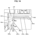
- FIG. 13 is an enlarged view of sensor 702 according to Exemplary Embodiment 4 having substantially the same structure as sensor 701 according to Embodiment 1.
- FIG. 14 is an enlarged view of sensor 702 shown in FIG. 13 for illustrating region R 409 .
- Sensor 702 according to Embodiment 4 has basically the same as sensor 701 according to Embodiment 1 shown in FIGS. 1 to 7 .
- Fixed electrode 433 a has side 4431 a that is disposed on the outer side relative to the edge of movable electrode 431 and side 4431 b that is set back inward relative to side 4431 a viewing from above.
- Side 4431 a is located outside the edge of movable electrode 431 by width W 301 viewing from above.
- width W 301 is 5 ⁇ m.
- Side 4431 b is aligned with the edge of movable electrode 431 viewing from above.
- straight line L 301 indicates the position of the edge of movable electrode 431 .
- Straight line L 301 serving as a boundary demarcates beam 432 b from movable electrode 431 .
- Beam 432 b deforms to warp due to an external acceleration applied thereto.
- Electrode 438 a has side 4481 a facing side 4431 a of fixed electrode 433 a , and side 4481 b facing side 4431 b of fixed electrode 433 a.
- Electrode 438 a does not only preventing the occurrence of sticking described earlier but also stabilizing the capacitance.
- FIG. 15 is a perspective view of sensor 1000 according to Exemplary Embodiment 5.
- Sensor 1000 includes package 5300 and a lid covering package 5300 . In FIG. 15 , the lid of package 5300 is not shown.
- Package 5300 accommodates sensor chip 5100 and integrated circuit 5200 for performing various calculations based on outputs from sensor chip 5100 .
- sensor 1000 is an acceleration sensor for detecting acceleration
- integrated circuit 5200 is an application-specific integrated circuit (ASIC).
- ASIC application-specific integrated circuit
- Terminals 5400 are led out from package 5300 to be connected to external board 5500 .
- Sensor 1000 is a capacitance-type acceleration sensor, and is manufactured by micro-electromechanical system (MEMS) technology.
- MEMS micro-electromechanical system
- FIG. 16 is an exploded perspective view of sensor chip 5100 .
- Sensor chip 5100 includes sensor part 501 , layer substrate 502 a joined to an upper surface of sensor part 501 , and layer substrate 502 b joined to a lower surface of sensor part 501 .
- Sensor part 501 is sandwiched between layer substrates 502 a and 502 b .
- Sensor part 501 is made of, e.g. a silicon-on-insulator (SOI) substrate.
- Layer substrates 502 a and 502 b are made of insulating material, such as glass.
- Sensor part 501 includes frame part 503 .
- Frame part 503 includes rectangular frames 510 a , 520 a , and 530 a which are arranged in a line.
- Movable electrode 511 is disposed inside rectangular frame 510 a .
- Movable electrode 521 is disposed inside rectangular frame 520 a .
- Movable electrode 531 is disposed inside rectangular frame 530 a.
- Sensor part 501 includes: X-detection part 510 detecting acceleration in a direction of the X-axis, Y-detection part 520 detecting acceleration in a direction of the Y-axis, and Z-detection part 530 detecting acceleration in a direction of the Z-axis.
- the X-axis is in parallel with both the upper and lower surfaces of sensor chip 5100 .
- the Y-axis is in parallel with both the upper and lower surfaces of sensor chip 5100 and is perpendicular to the X-axis.
- the Z-axis is perpendicular to both the X-axis and the Y-axis, that is, perpendicular to both the upper and lower surfaces of sensor chip 5100 .
- X-detection part 510 includes beams 512 a and 512 b , movable electrode 511 , and fixed electrodes 513 a and 513 b.
- Beams 512 a and 512 b are connected to rectangular frame 510 a to support movable electrode 511 .
- Beams 512 a and 512 b are arranged along straight line A 510 in parallel with the Y-axis.
- An upper surface of movable electrode 511 is divided into two sections by straight line A 510 .
- Fixed electrode 513 a faces one of the two sections of the upper surface of movable electrode 511 in the direction of the Z-axis with a space between fixed electrode 513 a and movable electrode 511 .
- Fixed electrode 513 b faces the other of the two sections of the upper surface of movable electrode 511 in the direction of the Z-axis with a space between fixed electrode 513 a and movable electrode 511 .
- X-detection part 510 detects acceleration in a direction of the X-axis based on both changes in capacitance between movable electrode 511 and fixed electrode 513 a and changes in capacitance between movable electrode 511 and fixed electrode 513 b.
- Y-detection part 520 includes beams 522 a and 522 b , movable electrode 521 , and fixed electrodes 523 a and 523 b .
- Y-detection part 520 has the same structure as X-detection part 510 with the structure being identical to that obtained by rotating X-detection part 510 on itself by 90 degrees.
- Each of the constituent members of Y-detection part 520 is the same in shape as the corresponding one of those of X-detection part 510 .
- Y-detection part 520 includes beams 522 a and 522 b , movable electrode 521 , and fixed electrodes 523 a and 523 b.
- Beams 522 a and 522 b are connected to rectangular frame 520 a and support movable electrode 521 .
- Beams 522 a and 522 b are arranged along straight line A 520 in parallel with the X-axis.
- An upper surface of movable electrode 521 is divided into two sections by straight line A 520 .
- Fixed electrode 523 a faces one of the two sections of the upper surface of movable electrode 521 in a direction of the Z-axis with a space between fixed electrode 523 a and movable electrode 521 .
- Fixed electrode 523 b faces the other of the two sections of the upper surface of movable electrode 521 in the direction of the Z-axis with a space between fixed electrode 523 b and movable electrode 521 .
- Y-detection part 520 detects acceleration in a direction of the Y-axis based on both changes in capacitance between movable electrode 521 and fixed electrode 523 a and changes in capacitance between movable electrode 521 and fixed electrode 523 b.
- beams 532 a , 532 b , 532 c , and 532 d are connected to rectangular frame 530 a and support movable electrode 531 .
- Fixed electrode 533 a faces an upper surface of movable electrode 531 in the direction of the Z-axis with a space between fixed electrode 533 a and movable electrode 531 .
- Fixed electrode 533 b faces a lower surface of movable electrode 531 in the direction of the Z-axis with a space between fixed electrode 533 b and movable electrode 531 .
- Z-detection part 530 detects acceleration in a the direction of the Z-axis based on both changes in capacitance between movable electrode 531 and fixed electrode 533 a and changes in capacitance between movable electrode 531 and fixed electrode 533 b.
- FIG. 17A is a cross-sectional view of X-detection part 510 .
- FIG. 17B is a cross-sectional view of Z-detection part 530 .
- a cross section of Y-detection part 520 is identical to that of X-detection part 510 .
- Fixed electrode 513 a and fixed electrode 513 b are led out to the upper surface of layer substrate 502 a through via-electrode 514 a and via-electrode 514 b , respectively.
- Fixed electrode 533 a is disposed on a portion of layer substrate 502 a facing movable electrode 531 .
- Fixed electrode 533 b is disposed on a portion of layer substrate 502 b facing movable electrode 531 . This configuration causes electrical signals from fixed electrode 533 a to be led out to the upper surface of layer substrate 502 a through via-electrode 534 a.
- Fixed electrode 533 b includes projection 533 b 2 that protrudes from rectangular region 533 b 1 (see FIG. 16 ). Projection 533 b 2 is connected to columnar fixed electrode 534 c that is separated away from movable electrode 531 . Columnar fixed electrode 534 c is connected to via-electrode 534 b that is disposed in layer substrate 502 a . This configuration allows electrical signals from fixed electrode 533 b to be led out to the upper surface of layer substrate 502 a through columnar fixed electrode 534 c and via-electrode 534 b.
- gap d changes, which in turn changes capacitance C.
- integrated circuit 5200 converts capacitance C into a voltage by capacitance-to-voltage (CV) conversion.
- Integrated circuit 5200 reduces the influence of a force on axes out of the tree axes other than the axis on which the acceleration is detected.
- FIGS. 18 and 19 are a cross-sectional view and a circuit diagram of X-detection part 510 , respectively, which does not have acceleration applied thereto in a direction of the X-axis.
- capacitance C 501 between movable electrode 511 and fixed electrode 513 a is equal to capacitance C 502 between movable electrode 511 and fixed electrode 513 b .
- Each of these capacitances is parasitic capacitance Cs 1 between movable electrode 511 and respective one of fixed electrodes 513 a and 513 b .
- FIGS. 20 and 21 are a cross-sectional view and a circuit diagram of X-detection part 510 , respectively, which has acceleration of 1 G applied thereto in a direction of the X-axis.
- capacitance C 501 between movable electrode 511 and fixed electrode 513 a is equal to the sum (Cs 1 + ⁇ C) of parasitic capacitance Cs 1 and change ⁇ C.
- Capacitance C 502 between movable electrode 511 and fixed electrode 513 b is equal to the difference (Cs 1 ⁇ C) obtained by subtracting change ⁇ C from parasitic capacitance Cs 1 .
- X-detection part 510 thus detects the acceleration in the X-direction based on changes in the capacitance.
- Y-detection part 520 detects the acceleration in the direction of the Y-axis, similarly to X-detection part 510 .
- FIGS. 22 and 23 are a cross-sectional view and a circuit diagram of Z-detection part 530 , respectively, which has acceleration of 1 G applied thereto in a direction of the Z-axis.
- capacitance C 505 between movable electrode 531 and fixed electrode 533 a is equal to a sum (Cs 2 + ⁇ C) of parasitic capacitance Cs 2 and change ⁇ C.
- Capacitance C 506 between movable electrode 531 and fixed electrode 533 b is equal to a difference (Cs 2 ⁇ C) obtained by subtracting change ⁇ C from parasitic capacitance Cs 2 .
- Z-detection part 530 thus detects the acceleration in the Z-direction based on changes in capacitance.
- the axis out of the three axes in the direction on which acceleration is detected is defined as a main axis.
- Each of axes out of the three axes other than the main axis is defined as one other axis.
- the following situation may be observed. That is, while acceleration in a direction of the main axis is applied, if the acceleration in a direction of one other axis is further applied, the output corresponding to the direction of the main axis indicates a value that is different from actual acceleration in the direction of the main axis.
- integrated circuit 5200 includes a correction circuit.
- the correction circuit reduces an influence of acceleration in the direction of one other axis on the output that indicates the acceleration in the direction of the main axis.
- the operation of sensor 1000 will be described as a reference state and a correction state.
- the reference state is a case that no acceleration is applied in directions of other axes.
- the correction state is a case that acceleration is applied in a direction of one other axis and a correction is necessary.
- the operation of sensor 1000 will be described in the case where the X-axis is the main axis while the Z-axis is the one other axis.
- FIG. 24A illustrates an output of X-detection part 510 in the reference state while the output indicates acceleration in a direction of the X-axis, i.e. the main axis, of sensor 1000 .
- FIG. 24B illustrates an output of Z-detection part 530 while the output indicating acceleration in the direction of the Z-axis, i.e. the one other axis.
- FIG. 24C is a cross-sectional view of X-detection part 510 that is detecting the acceleration in the direction of the X-axis, i.e. the main axis.
- straight lines O 511 and O 521 indicate ideal outputs while curved lines O 512 and O 522 indicate actual outputs.
- the output of an ideal sensor is proportional to the applied acceleration; however, the actual output contains error. For this reason, only the output within linear region E 501 in which the output is proportional to the applied acceleration may be used. Alternatively, in addition to this, the output outside linear region E 501 may also be used after being corrected by integrated circuit 5200 .
- FIG. 25A illustrates an output of X-detection part 510 in the correction state while the output indicates acceleration in the direction of the X-axis, i.e. the main axis.
- FIG. 25B is a graph showing an output of Z-detection part 530 in the correction state while the output indicates acceleration in the direction of the Z-axis, i.e. the one other axis.
- FIG. 25C is a cross-sectional view of X-detection part 510 in the correction state.
- influence of the one other axis is relatively large. Therefore, as shown in FIG. 25A , the difference between curved line O 513 that indicates the output for the main axis and straight line O 511 that indicates an ideal output is larger than that in the reference state.
- movable electrode 511 is tilted largely and reduces gap d accordingly.
- Such small gap d increases change ⁇ C, and increases sensitivity accordingly.
- FIG. 26 is a functional block diagram of sensor 1000 according to Embodiment 5.
- Integrated circuit 5200 includes correction circuit 5210 that corrects the sensitivity for the axes. The sensitivity changes according to the change of gap d. An operation of correction circuit 5210 will be described below.
- the correction circuit of the comparative example corrects output Xout 1 supplied from X-detection part 510 to provide output Xout 2 while the output is produced in accordance with acceleration in the direction of the X-axis, the main axis.
- Output Xout 2 is a signal that is obtained by subtracting an other-axis sensitivity from output Xout 1 .
- the other-axis sensitivity is an offset that is contained in output Xout 1 . The offset results from the acceleration in the direction of the Z-axis, i.e. the one other axis.
- the correction circuit of the comparative example provides output Xout 2 by Equation 1 with a correction coefficient AGCcode and the output Zout supplied from Z-detection part 530 in accordance with the acceleration in the direction of the Z-axis, the one other axis.
- X out2 X out1/(1 ⁇ AGCcode ⁇ Z out) (1)
- the correction circuit of the comparative example corrects output Xout 1 by changing correction factor (1/(1 ⁇ AGCcode ⁇ Zout)). Specifically, output Xout 1 is lineally corrected such that output Xout 1 is amplified when output Zout is positive and that output Xout 1 is attenuated when output Zout is negative.
- FIG. 27 illustrates a sensitivity of X-detection part 510 for the acceleration in the direction of the X-axis, i.e. the main axis with respect to the acceleration in the direction of the Z-axis, i.e. the one other axis.
- FIG. 27 experimental results have shown that changes in sensitivity of X-detection part 510 are different depending on whether the acceleration applied in parallel with the Z-axis is positive or negative.
- the changes in sensitivity results from changes in gap d of X-detection part 510 caused by the acceleration applied to the Z-direction.
- negative acceleration in the Z-axis i.e. acceleration in the negative direction of the Z-axis applied thereto decreases gap d, and increase a change in the sensitivity for the acceleration in the direction of the X-axis.
- positive acceleration in the Z-axis i.e. acceleration in the positive direction opposite to the negative direction of the Z-axis increases gap d, and decreases a change in the sensitivity for the acceleration in the direction of the X-axis.
- the change in the sensitivity of X-detection part 510 is different depending on the direction of the acceleration in parallel with the Z-axis.
- FIGS. 28A and 28B illustrate outputs obtained by correcting outputs of X-detection part 510 obtained by the correction circuit of the sensor of the comparative example.
- the correction is made by Equation 1 used in the correction circuit of the sensor of the comparative example as follows.
- correction coefficient AGCcode is determined by calculation based on the acceleration in the positive direction of the Z-axis such that the change in sensitivity for the acceleration in the direction of the X-axis becomes zero
- the resulting correction is as follows: The sensitivity for the acceleration in the direction of the X-axis changes against the acceleration in the negative direction of the Z-axis, not correcting output Xout 1 properly, as shown in FIG. 28A .
- correction coefficient AGCcode is determined by calculation based on the acceleration in the negative direction of the Z-axis such that the change in sensitivity for the acceleration in the direction of the X-axis becomes zero
- the resulting correction is as follows: The sensitivity changes against the acceleration in the positive direction of the Z-axis, not correcting output Xout 1 properly, as shown in FIG. 28B .
- Correction circuit 5210 of sensor 1000 according to Embodiment 5 is configured such that an equation for use in correction is changed in accordance with the direction of the acceleration in parallel with the Z-axis. Specifically, correction circuit 5210 operates as follows: In cases where the acceleration in parallel with the Z-axis is in the positive direction of the Z-axis (Zout>0), the following Equation 2 including weighting variable W 501 is used to correct output Xout 1 of X-detection part 510 , thereby providing output Xout 2 .
- Equation 3 weighting variable W 502 is used to correct output Xout 1 of X-detection part 510 , thereby providing output Xout 2 .
- X out2 X out1/(1 ⁇ AGCcode ⁇ Z out ⁇ W 501) ( Z out>0)
- X out2 X out1/(1 ⁇ AGCcode ⁇ Z out ⁇ W 502) ( Z out ⁇ 0) (3)
- Weighting variables W 501 and W 502 are variables for weighing the correction coefficient, and are determined in the following manner.
- positive-side sensitivity Sp is determined.
- Positive-side sensitivity Sp is the sensitivity of X-detection part 510 for acceleration in the direction of the X-axis when acceleration of a certain magnitude in the positive direction of the Z-axis is being applied.
- negative-side sensitivity Sn is determined.
- Negative-side sensitivity Sn is the sensitivity of X-detection part 510 for acceleration in the direction of the X-axis when acceleration of the magnitude equal to that of the negative direction of the Z-axis is applied.
- an equation for use in correction is changed in accordance with positive and negative (direction) of acceleration in the direction of the Z-axis” used herein means that “at least two equations are usable for cases where the acceleration in the direction of the Z-axis is positive and negative.”
- the term does not mean “only equations, i.e. one is used for cases where the acceleration in the direction of the Z-axis is positive and the other is used for cases where the acceleration is negative, with a boundary corresponding to the acceleration of zero.”
- a selection of one from the equations may be made so as to choose which of the directions, i.e. positive and negative, of acceleration in the Z-axis is used to calculate output Xout 2 that can correctly correspond to the acceleration to be measured.
- This configuration accurately reduces the influence of the acceleration in the one other axis regardless of positive and negative signs (directions) the acceleration in the Z-axis, i.e. of the one other axis.
- the influence of the acceleration in the direction of one other axis on the output that indicates the acceleration in the direction of the main axis can be relieved to improve the output characteristics of the detection part for detecting the acceleration in the main axis.
- correction circuit 5210 may correct output Xout 1 in the following way that uses other equations.
- values of the sensitivity of X-detection part 510 is measured for different cases where different measurement of acceleration with a certain identical magnitude is carried out for different acceleration directions, i.e. the positive and the negative in the Z-axis.
- the average of the measured values of the sensitivity of X-detection part 510 is determined to be a target value.
- correction coefficient AGCcode 1 is determined such that output Xout 21 becomes equal to the target value.
- X out21 X out1/(1 ⁇ AGCcode1 ⁇ Z out) (4)
- FIG. 29A illustrates the output characteristics of X-detection part 510 obtained by using Equation 4.
- Equations 4 and 5 can relieve the influence of the acceleration in the direction of the one other axis on the output that indicates the acceleration in the direction of the main axis, thereby improving the output characteristics in the main axis.
- FIG. 29B illustrates the output characteristics of output Xout 22 that is corrected by using Equation 5.
- the sensitivity of Y-detection part 520 can be corrected by the same method as the correction of the sensitivity of X-detection part 510 .
- the X-axis (Y-axis) is the main axis while the Z-axis is the one other axis; however, the main axis and the one other axis may be appropriately changed.
- three units of MEMS structures (X-detection part 510 , Y-detection part 520 , and Z-detection part 530 ) are disposed in the single chip while each of the three units is used for detecting acceleration in the corresponding one of the three axes, i.e. the X-axis, Y-axis, and Z-axis.
- the output in the main axis can be corrected in accordance with the output in one other axis while the three outputs are the output indicating acceleration in the direction in the X-axis, output indicating acceleration in the direction in the Y-axis, and output indicating acceleration in the direction in the Z-axis.
- Sensor chip 5100 may be appropriately modified in, e.g. shape, size, or arrangement.
- the material of the via-electrodes is conductive material, such as silicon, tungsten, or copper.
- the material of a part surrounding and holding the via-electrodes is insulating material, such as glass.
- the shape of beams 532 a , 532 b , 532 c , and 532 d is not necessarily the L-shape; however, the L-shape preferably allows beams 532 a , 532 b , 532 c , and 532 d to have large lengths.
- Correction circuit 5210 preferably performs arithmetic corrections with a digital circuit. Arithmetic corrections with the digital circuit can perform various kinds of corrections including sensitivity adjustment and offset adjustment, for example.
Landscapes
- Physics & Mathematics (AREA)
- General Physics & Mathematics (AREA)
- Pressure Sensors (AREA)
Abstract
Description
Xout2=Xout1/(1−AGCcode×Zout) (1)
Xout2=Xout1/(1−AGCcode×Zout×W501) (Zout>0) (2)
Xout2=Xout1/(1−AGCcode×Zout×W502) (Zout≤0) (3)
Xout21=Xout1/(1−AGCcode1×Zout) (4)
Xout22=Xout21/(1+|AGCcode2×Zout|) (5)
- 401 sensor substrate
- 402 a layer substrate (first layer substrate)
- 402 b layer substrate (second layer substrate)
- 403 connection part
- 410 X-detection part
- 410 a rectangular frame
- 411 movable electrode
- 412 a, 412 b beam
- 413 a, 413 b fixed electrode
- 414 a, 414 b via-electrode
- 420 Y-detection part
- 420 a rectangular frame
- 421 movable electrode
- 422 a, 422 b beam
- 423 a, 423 b fixed electrode
- 424 a, 424 b via-electrode
- 430 Z-detection part
- 430 a rectangular frame
- 431 movable electrode
- 432 a, 432 b, 432 c, 432 d beam
- 433 a, 433 b fixed electrode
- 434 a, 434 b via-electrode
- 435 a columnar electrode
- 435 b columnar electrode
- 435 c columnar electrode
- 435 d columnar electrode
- 438 a, 438 b, 438 c electrode
- 439 a, 439 b, 439 c, 439 d, 439 e wire
- 441 a, 441 b, 441 c, 441 d connection part
- 442 a, 442 b, 442 c, 442 d projection
- 444 oxide film
- 4100 sensor chip
- 4200 integrated circuit
- 4300 package
- 4302 space
- 4400 terminal
- 4402 lead
- 4402 c end
- 4404 ground
- 4600 lid
- 491, 492 groove
- 501 sensor part
- 502 a layer substrate
- 502 b layer substrate
- 503 frame part
- 510 X-detection part
- 510 a rectangular frame
- 511 movable electrode
- 512 a, 512 b beam
- 513 a, 513 b fixed electrode
- 514 a, 514 b via-electrode
- 520 Y-detection part
- 520 a rectangular frame
- 521 movable electrode
- 522 a, 522 b beam
- 523 a, 523 b fixed electrode
- 530 Z-detection part
- 530 a rectangular frame
- 531 movable electrode
- 532 a, 532 b, 532 c, 532 d beam
- 533 a, 533 b fixed electrode
- 533 b 1 rectangular region
- 533 b 2 projection
- 534 a via-electrode
- 534 b via-electrode
- 534 c fixed electrode
- 5210 correction circuit
- 5100 sensor chip
- 5200 integrated circuit
- 5300 package
- 5400 terminal
- 5500 board
- 1000 sensor
Claims (6)
Applications Claiming Priority (11)
| Application Number | Priority Date | Filing Date | Title |
|---|---|---|---|
| JP2015-245850 | 2015-12-17 | ||
| JP2015245850 | 2015-12-17 | ||
| JP2015-248157 | 2015-12-21 | ||
| JP2015248157 | 2015-12-21 | ||
| JP2015-248158 | 2015-12-21 | ||
| JP2015248158 | 2015-12-21 | ||
| JP2015250136 | 2015-12-22 | ||
| JP2015-250136 | 2015-12-22 | ||
| JP2016-057958 | 2016-03-23 | ||
| JP2016057958 | 2016-03-23 | ||
| PCT/JP2016/004792 WO2017104103A1 (en) | 2015-12-17 | 2016-11-02 | Connecting structure |
Publications (2)
| Publication Number | Publication Date |
|---|---|
| US20180267079A1 US20180267079A1 (en) | 2018-09-20 |
| US10649000B2 true US10649000B2 (en) | 2020-05-12 |
Family
ID=59056181
Family Applications (1)
| Application Number | Title | Priority Date | Filing Date |
|---|---|---|---|
| US15/760,615 Active 2037-03-31 US10649000B2 (en) | 2015-12-17 | 2016-11-02 | Connection assembly |
Country Status (3)
| Country | Link |
|---|---|
| US (1) | US10649000B2 (en) |
| JP (1) | JP6704126B2 (en) |
| WO (1) | WO2017104103A1 (en) |
Families Citing this family (2)
| Publication number | Priority date | Publication date | Assignee | Title |
|---|---|---|---|---|
| JP2020101484A (en) | 2018-12-25 | 2020-07-02 | セイコーエプソン株式会社 | Inertia sensor, electronic apparatus and moving body |
| US11754593B2 (en) * | 2019-03-26 | 2023-09-12 | Panasonic Intellectual Property Management Co., Ltd. | Signal processing device, inertial sensor, signal processing method, and program |
Citations (47)
| Publication number | Priority date | Publication date | Assignee | Title |
|---|---|---|---|---|
| US3737729A (en) * | 1971-06-14 | 1973-06-05 | Zeltex Inc | Electronic package and method of construction |
| JPS57655B2 (en) | 1977-12-12 | 1982-01-07 | ||
| US4879589A (en) * | 1988-01-25 | 1989-11-07 | Semetex Corporation | Hermetic leadless semiconductor device package |
| JPH07113708A (en) | 1993-10-20 | 1995-05-02 | Hitachi Ltd | Method of manufacturing semiconductor absolute pressure sensor |
| US5426563A (en) * | 1992-08-05 | 1995-06-20 | Fujitsu Limited | Three-dimensional multichip module |
| US5568361A (en) * | 1992-03-17 | 1996-10-22 | Massachusetts Institute Of Technology | Three-dimensional electronic circuit of interconnected modules |
| US5616521A (en) * | 1995-04-07 | 1997-04-01 | Sensym, Incorporated | Side port package for micromachined fluid sensor |
| US5691885A (en) * | 1992-03-17 | 1997-11-25 | Massachusetts Institute Of Technology | Three-dimensional interconnect having modules with vertical top and bottom connectors |
| US5854534A (en) * | 1992-08-05 | 1998-12-29 | Fujitsu Limited | Controlled impedence interposer substrate |
| US5864062A (en) * | 1996-11-18 | 1999-01-26 | Mitsubishi Denki Kabushiki Kaisha | Semiconductor acceleration sensor |
| JPH1123610A (en) | 1997-07-08 | 1999-01-29 | Omron Corp | Capacitive multi-axis acceleration detector |
| US6040625A (en) * | 1997-09-25 | 2000-03-21 | I/O Sensors, Inc. | Sensor package arrangement |
| JP2000164741A (en) | 1998-11-26 | 2000-06-16 | Toyota Motor Corp | Semiconductor device |
| US6369445B1 (en) * | 2000-06-19 | 2002-04-09 | Advantest Corporation | Method and apparatus for edge connection between elements of an integrated circuit |
| US6404046B1 (en) * | 2000-02-03 | 2002-06-11 | Amkor Technology, Inc. | Module of stacked integrated circuit packages including an interposer |
| US6440775B2 (en) * | 2000-06-19 | 2002-08-27 | Advantest Corporation | Method and apparatus for edge connection between elements of an integrated circuit |
| US6492699B1 (en) * | 2000-05-22 | 2002-12-10 | Amkor Technology, Inc. | Image sensor package having sealed cavity over active area |
| US6518659B1 (en) * | 2000-05-08 | 2003-02-11 | Amkor Technology, Inc. | Stackable package having a cavity and a lid for an electronic device |
| US20060163679A1 (en) * | 2005-01-21 | 2006-07-27 | Honeywell International, Inc. | High performance MEMS packaging architecture |
| US20060169042A1 (en) * | 2002-04-29 | 2006-08-03 | Hulsing Rand H Ii | Closed loop analog gyro rate sensor |
| US20070022814A1 (en) * | 2005-07-27 | 2007-02-01 | Masami Seto | Semiconductor sensor |
| US20070132047A1 (en) * | 2005-11-23 | 2007-06-14 | Heikki Kuisma | Method for manufacturing a microelectromechanical component, and a microelectromechanical component |
| US20080073739A1 (en) * | 2005-05-26 | 2008-03-27 | Murata Manufacturing Co., Ltd. | Electronic component package, electronic component using the package, and method for manufacturing electronic component package |
| US20080128848A1 (en) * | 2006-11-30 | 2008-06-05 | Sony Corporation | Solid-state imaging device |
| US7419382B2 (en) * | 2005-10-31 | 2008-09-02 | Kabushiki Kaisha Toshiba | Printed circuit board, electronic device, and manufacturing method for printed circuit board |
| US20090261432A1 (en) * | 2008-03-26 | 2009-10-22 | Leslie Bruce Wilner | Interconnection system on a plane adjacent to a solid-state device structure |
| US20100072862A1 (en) * | 2008-09-23 | 2010-03-25 | Custom Sensors & Technologies, Inc. | Inertial sensor with dual cavity package and method of fabrication |
| US7936176B2 (en) * | 2004-06-21 | 2011-05-03 | Capres A/S | Method for providing alignment of a probe |
| JP4692373B2 (en) | 2006-04-28 | 2011-06-01 | パナソニック電工株式会社 | Capacitive sensor |
| US20110265564A1 (en) * | 2010-04-30 | 2011-11-03 | Qualcomm Mems Technologies, Inc. | Micromachined piezoelectric x-axis gyroscope |
| US20120012949A1 (en) * | 2010-07-13 | 2012-01-19 | Bernhard Winkler | Pressure sensor package systems and methods |
| US8193555B2 (en) * | 2009-02-11 | 2012-06-05 | Megica Corporation | Image and light sensor chip packages |
| JP2013079895A (en) | 2011-10-05 | 2013-05-02 | Panasonic Corp | Semiconductor physical quantity sensor |
| US20130193532A1 (en) * | 2012-01-27 | 2013-08-01 | Wacom Co., Ltd. | Capacitive pressure sensing semiconductor device |
| US20130307094A1 (en) * | 2011-03-11 | 2013-11-21 | Panasonic Corporation | Sensor |
| US20130313663A1 (en) * | 2011-02-11 | 2013-11-28 | Canon Kabushiki Kaisha | Capacitive electromechanical transducer |
| US20140027868A1 (en) * | 2011-04-21 | 2014-01-30 | Hitachi, Ltd. | Mechanical quantity measuring device |
| US8742545B2 (en) * | 2009-04-15 | 2014-06-03 | Sunovel Suzhou Technologies Ltd. | Substrate strip plate structure for semiconductor device and method of manufacturing the same |
| US8810023B2 (en) * | 2012-07-06 | 2014-08-19 | Texas Instruments Incorporated | Cantilever packages for sensor MEMS (micro-electro-mechanical system) |
| JP2014238280A (en) | 2013-06-06 | 2014-12-18 | パナソニックIpマネジメント株式会社 | Acceleration sensor |
| JP2015010856A (en) | 2013-06-27 | 2015-01-19 | パナソニック株式会社 | Acceleration sensor |
| US20150260752A1 (en) | 2012-10-12 | 2015-09-17 | Panasonic Corporation | Acceleration sensor |
| US20160013112A1 (en) * | 2013-02-21 | 2016-01-14 | Epcos Ag | Sensor System Comprising a Ceramic Housing |
| US20170336436A1 (en) * | 2015-01-15 | 2017-11-23 | Panasonic Intellectual Property Management Co., Ltd. | Sensor |
| US20170345949A1 (en) * | 2014-12-24 | 2017-11-30 | Fujikura Ltd. | Pressure sensor and pressure sensor module |
| US10015882B1 (en) * | 2015-01-05 | 2018-07-03 | Qorvo Us, Inc. | Modular semiconductor package |
| US10240953B2 (en) * | 2014-02-17 | 2019-03-26 | Robert Bosch Gmbh | Housing with a damping element for a micromechanical sensor element |
Family Cites Families (4)
| Publication number | Priority date | Publication date | Assignee | Title |
|---|---|---|---|---|
| DE3735455A1 (en) * | 1987-03-18 | 1988-09-29 | Telefonbau & Normalzeit Gmbh | ELECTRICAL COMPONENTS |
| KR100393452B1 (en) * | 1998-09-16 | 2003-08-02 | 가부시키가이샤 히타치세이사쿠쇼 | A substrate unit processing of a semiconductor element check |
| JP5493767B2 (en) * | 2009-11-25 | 2014-05-14 | 大日本印刷株式会社 | Sensor unit and manufacturing method thereof |
| US20170089941A1 (en) * | 2014-04-08 | 2017-03-30 | Panasonic Intellectual Property Management Co., Ltd. | Sensor |
-
2016
- 2016-11-02 WO PCT/JP2016/004792 patent/WO2017104103A1/en not_active Ceased
- 2016-11-02 US US15/760,615 patent/US10649000B2/en active Active
- 2016-11-02 JP JP2017556317A patent/JP6704126B2/en not_active Expired - Fee Related
Patent Citations (47)
| Publication number | Priority date | Publication date | Assignee | Title |
|---|---|---|---|---|
| US3737729A (en) * | 1971-06-14 | 1973-06-05 | Zeltex Inc | Electronic package and method of construction |
| JPS57655B2 (en) | 1977-12-12 | 1982-01-07 | ||
| US4879589A (en) * | 1988-01-25 | 1989-11-07 | Semetex Corporation | Hermetic leadless semiconductor device package |
| US5568361A (en) * | 1992-03-17 | 1996-10-22 | Massachusetts Institute Of Technology | Three-dimensional electronic circuit of interconnected modules |
| US5691885A (en) * | 1992-03-17 | 1997-11-25 | Massachusetts Institute Of Technology | Three-dimensional interconnect having modules with vertical top and bottom connectors |
| US5426563A (en) * | 1992-08-05 | 1995-06-20 | Fujitsu Limited | Three-dimensional multichip module |
| US5854534A (en) * | 1992-08-05 | 1998-12-29 | Fujitsu Limited | Controlled impedence interposer substrate |
| JPH07113708A (en) | 1993-10-20 | 1995-05-02 | Hitachi Ltd | Method of manufacturing semiconductor absolute pressure sensor |
| US5616521A (en) * | 1995-04-07 | 1997-04-01 | Sensym, Incorporated | Side port package for micromachined fluid sensor |
| US5864062A (en) * | 1996-11-18 | 1999-01-26 | Mitsubishi Denki Kabushiki Kaisha | Semiconductor acceleration sensor |
| JPH1123610A (en) | 1997-07-08 | 1999-01-29 | Omron Corp | Capacitive multi-axis acceleration detector |
| US6040625A (en) * | 1997-09-25 | 2000-03-21 | I/O Sensors, Inc. | Sensor package arrangement |
| JP2000164741A (en) | 1998-11-26 | 2000-06-16 | Toyota Motor Corp | Semiconductor device |
| US6404046B1 (en) * | 2000-02-03 | 2002-06-11 | Amkor Technology, Inc. | Module of stacked integrated circuit packages including an interposer |
| US6518659B1 (en) * | 2000-05-08 | 2003-02-11 | Amkor Technology, Inc. | Stackable package having a cavity and a lid for an electronic device |
| US6492699B1 (en) * | 2000-05-22 | 2002-12-10 | Amkor Technology, Inc. | Image sensor package having sealed cavity over active area |
| US6369445B1 (en) * | 2000-06-19 | 2002-04-09 | Advantest Corporation | Method and apparatus for edge connection between elements of an integrated circuit |
| US6440775B2 (en) * | 2000-06-19 | 2002-08-27 | Advantest Corporation | Method and apparatus for edge connection between elements of an integrated circuit |
| US20060169042A1 (en) * | 2002-04-29 | 2006-08-03 | Hulsing Rand H Ii | Closed loop analog gyro rate sensor |
| US7936176B2 (en) * | 2004-06-21 | 2011-05-03 | Capres A/S | Method for providing alignment of a probe |
| US20060163679A1 (en) * | 2005-01-21 | 2006-07-27 | Honeywell International, Inc. | High performance MEMS packaging architecture |
| US20080073739A1 (en) * | 2005-05-26 | 2008-03-27 | Murata Manufacturing Co., Ltd. | Electronic component package, electronic component using the package, and method for manufacturing electronic component package |
| US20070022814A1 (en) * | 2005-07-27 | 2007-02-01 | Masami Seto | Semiconductor sensor |
| US7419382B2 (en) * | 2005-10-31 | 2008-09-02 | Kabushiki Kaisha Toshiba | Printed circuit board, electronic device, and manufacturing method for printed circuit board |
| US20070132047A1 (en) * | 2005-11-23 | 2007-06-14 | Heikki Kuisma | Method for manufacturing a microelectromechanical component, and a microelectromechanical component |
| JP4692373B2 (en) | 2006-04-28 | 2011-06-01 | パナソニック電工株式会社 | Capacitive sensor |
| US20080128848A1 (en) * | 2006-11-30 | 2008-06-05 | Sony Corporation | Solid-state imaging device |
| US20090261432A1 (en) * | 2008-03-26 | 2009-10-22 | Leslie Bruce Wilner | Interconnection system on a plane adjacent to a solid-state device structure |
| US20100072862A1 (en) * | 2008-09-23 | 2010-03-25 | Custom Sensors & Technologies, Inc. | Inertial sensor with dual cavity package and method of fabrication |
| US8193555B2 (en) * | 2009-02-11 | 2012-06-05 | Megica Corporation | Image and light sensor chip packages |
| US8742545B2 (en) * | 2009-04-15 | 2014-06-03 | Sunovel Suzhou Technologies Ltd. | Substrate strip plate structure for semiconductor device and method of manufacturing the same |
| US20110265564A1 (en) * | 2010-04-30 | 2011-11-03 | Qualcomm Mems Technologies, Inc. | Micromachined piezoelectric x-axis gyroscope |
| US20120012949A1 (en) * | 2010-07-13 | 2012-01-19 | Bernhard Winkler | Pressure sensor package systems and methods |
| US20130313663A1 (en) * | 2011-02-11 | 2013-11-28 | Canon Kabushiki Kaisha | Capacitive electromechanical transducer |
| US20130307094A1 (en) * | 2011-03-11 | 2013-11-21 | Panasonic Corporation | Sensor |
| US20140027868A1 (en) * | 2011-04-21 | 2014-01-30 | Hitachi, Ltd. | Mechanical quantity measuring device |
| JP2013079895A (en) | 2011-10-05 | 2013-05-02 | Panasonic Corp | Semiconductor physical quantity sensor |
| US20130193532A1 (en) * | 2012-01-27 | 2013-08-01 | Wacom Co., Ltd. | Capacitive pressure sensing semiconductor device |
| US8810023B2 (en) * | 2012-07-06 | 2014-08-19 | Texas Instruments Incorporated | Cantilever packages for sensor MEMS (micro-electro-mechanical system) |
| US20150260752A1 (en) | 2012-10-12 | 2015-09-17 | Panasonic Corporation | Acceleration sensor |
| US20160013112A1 (en) * | 2013-02-21 | 2016-01-14 | Epcos Ag | Sensor System Comprising a Ceramic Housing |
| JP2014238280A (en) | 2013-06-06 | 2014-12-18 | パナソニックIpマネジメント株式会社 | Acceleration sensor |
| JP2015010856A (en) | 2013-06-27 | 2015-01-19 | パナソニック株式会社 | Acceleration sensor |
| US10240953B2 (en) * | 2014-02-17 | 2019-03-26 | Robert Bosch Gmbh | Housing with a damping element for a micromechanical sensor element |
| US20170345949A1 (en) * | 2014-12-24 | 2017-11-30 | Fujikura Ltd. | Pressure sensor and pressure sensor module |
| US10015882B1 (en) * | 2015-01-05 | 2018-07-03 | Qorvo Us, Inc. | Modular semiconductor package |
| US20170336436A1 (en) * | 2015-01-15 | 2017-11-23 | Panasonic Intellectual Property Management Co., Ltd. | Sensor |
Non-Patent Citations (1)
| Title |
|---|
| International Search Report of PCT application No. PCT/JP2016/004792 dated Jan. 31, 2017. |
Also Published As
| Publication number | Publication date |
|---|---|
| JP6704126B2 (en) | 2020-06-03 |
| WO2017104103A1 (en) | 2017-06-22 |
| JPWO2017104103A1 (en) | 2018-10-04 |
| US20180267079A1 (en) | 2018-09-20 |
Similar Documents
| Publication | Publication Date | Title |
|---|---|---|
| CN1954188B (en) | Gyro sensor and sensor device using the gyro sensor | |
| US8096187B2 (en) | Pressure sensor element and pressure sensor | |
| JP4931713B2 (en) | Mechanical quantity sensor | |
| US8201450B2 (en) | Angular velocity sensor | |
| JP5427199B2 (en) | Semiconductor physical quantity detection sensor | |
| US9857258B2 (en) | Pressure sensor to sense multi-directional movement | |
| US20050217377A1 (en) | Physical quantity sensor having angular speed sensor and acceleration sensor | |
| US10649000B2 (en) | Connection assembly | |
| US20160341759A1 (en) | Sensor and method of manufacturing same | |
| US8026594B2 (en) | Sensor device and production method therefor | |
| JP2016070670A (en) | Sensor device | |
| WO2018116549A1 (en) | Pressure sensor element and pressure sensor module provided with same | |
| JP2015010856A (en) | Acceleration sensor | |
| JP2018115891A (en) | Acceleration sensor | |
| US20090255343A1 (en) | Physical quantity sensor and method for manufacturing the same | |
| US20160091526A1 (en) | Sensor | |
| US20060086185A1 (en) | Acceleration sensor | |
| JP2023175166A (en) | Inertial measuring device | |
| JPH06265569A (en) | Acceleration sensor unit | |
| JP2000121475A (en) | Capacitive pressure detector | |
| US20240053377A1 (en) | Acceleration sensor | |
| JP2015017819A (en) | Acceleration sensor | |
| US20240061010A1 (en) | Acceleration sensor | |
| JP5194510B2 (en) | Sensor device | |
| US20080237839A1 (en) | Semiconductor apparatus and method of manufacturing same |
Legal Events
| Date | Code | Title | Description |
|---|---|---|---|
| FEPP | Fee payment procedure |
Free format text: ENTITY STATUS SET TO UNDISCOUNTED (ORIGINAL EVENT CODE: BIG.); ENTITY STATUS OF PATENT OWNER: LARGE ENTITY |
|
| AS | Assignment |
Owner name: PANASONIC INTELLECTUAL PROPERTY MANAGEMENT CO., LTD., JAPAN Free format text: ASSIGNMENT OF ASSIGNORS INTEREST;ASSIGNORS:SHINOHARA, TAKAHIRO;YOSHIDA, HITOSHI;GODA, KAZUO;AND OTHERS;SIGNING DATES FROM 20180208 TO 20180213;REEL/FRAME:045825/0791 Owner name: PANASONIC INTELLECTUAL PROPERTY MANAGEMENT CO., LT Free format text: ASSIGNMENT OF ASSIGNORS INTEREST;ASSIGNORS:SHINOHARA, TAKAHIRO;YOSHIDA, HITOSHI;GODA, KAZUO;AND OTHERS;SIGNING DATES FROM 20180208 TO 20180213;REEL/FRAME:045825/0791 |
|
| STPP | Information on status: patent application and granting procedure in general |
Free format text: DOCKETED NEW CASE - READY FOR EXAMINATION |
|
| STPP | Information on status: patent application and granting procedure in general |
Free format text: NOTICE OF ALLOWANCE MAILED -- APPLICATION RECEIVED IN OFFICE OF PUBLICATIONS |
|
| STCF | Information on status: patent grant |
Free format text: PATENTED CASE |
|
| MAFP | Maintenance fee payment |
Free format text: PAYMENT OF MAINTENANCE FEE, 4TH YEAR, LARGE ENTITY (ORIGINAL EVENT CODE: M1551); ENTITY STATUS OF PATENT OWNER: LARGE ENTITY Year of fee payment: 4 |