US10644714B2 - Pipelined analog-to-digital converter - Google Patents
Pipelined analog-to-digital converter Download PDFInfo
- Publication number
- US10644714B2 US10644714B2 US16/358,456 US201916358456A US10644714B2 US 10644714 B2 US10644714 B2 US 10644714B2 US 201916358456 A US201916358456 A US 201916358456A US 10644714 B2 US10644714 B2 US 10644714B2
- Authority
- US
- United States
- Prior art keywords
- output
- flash converter
- converter
- adc
- comparators
- Prior art date
- Legal status (The legal status is an assumption and is not a legal conclusion. Google has not performed a legal analysis and makes no representation as to the accuracy of the status listed.)
- Active
Links
Images


Classifications
-
- H—ELECTRICITY
- H03—ELECTRONIC CIRCUITRY
- H03M—CODING; DECODING; CODE CONVERSION IN GENERAL
- H03M1/00—Analogue/digital conversion; Digital/analogue conversion
- H03M1/06—Continuously compensating for, or preventing, undesired influence of physical parameters
- H03M1/0617—Continuously compensating for, or preventing, undesired influence of physical parameters characterised by the use of methods or means not specific to a particular type of detrimental influence
- H03M1/0675—Continuously compensating for, or preventing, undesired influence of physical parameters characterised by the use of methods or means not specific to a particular type of detrimental influence using redundancy
- H03M1/069—Continuously compensating for, or preventing, undesired influence of physical parameters characterised by the use of methods or means not specific to a particular type of detrimental influence using redundancy by range overlap between successive stages or steps
- H03M1/0695—Continuously compensating for, or preventing, undesired influence of physical parameters characterised by the use of methods or means not specific to a particular type of detrimental influence using redundancy by range overlap between successive stages or steps using less than the maximum number of output states per stage or step, e.g. 1.5 per stage or less than 1.5 bit per stage type
-
- H—ELECTRICITY
- H03—ELECTRONIC CIRCUITRY
- H03M—CODING; DECODING; CODE CONVERSION IN GENERAL
- H03M1/00—Analogue/digital conversion; Digital/analogue conversion
- H03M1/12—Analogue/digital converters
- H03M1/1205—Multiplexed conversion systems
- H03M1/121—Interleaved, i.e. using multiple converters or converter parts for one channel
- H03M1/1215—Interleaved, i.e. using multiple converters or converter parts for one channel using time-division multiplexing
-
- H—ELECTRICITY
- H03—ELECTRONIC CIRCUITRY
- H03F—AMPLIFIERS
- H03F3/00—Amplifiers with only discharge tubes or only semiconductor devices as amplifying elements
- H03F3/04—Amplifiers with only discharge tubes or only semiconductor devices as amplifying elements with semiconductor devices only
-
- H—ELECTRICITY
- H03—ELECTRONIC CIRCUITRY
- H03F—AMPLIFIERS
- H03F3/00—Amplifiers with only discharge tubes or only semiconductor devices as amplifying elements
- H03F3/45—Differential amplifiers
- H03F3/45071—Differential amplifiers with semiconductor devices only
- H03F3/45076—Differential amplifiers with semiconductor devices only characterised by the way of implementation of the active amplifying circuit in the differential amplifier
- H03F3/45179—Differential amplifiers with semiconductor devices only characterised by the way of implementation of the active amplifying circuit in the differential amplifier using MOSFET transistors as the active amplifying circuit
- H03F3/45183—Long tailed pairs
- H03F3/45188—Non-folded cascode stages
-
- H—ELECTRICITY
- H03—ELECTRONIC CIRCUITRY
- H03M—CODING; DECODING; CODE CONVERSION IN GENERAL
- H03M1/00—Analogue/digital conversion; Digital/analogue conversion
- H03M1/12—Analogue/digital converters
- H03M1/14—Conversion in steps with each step involving the same or a different conversion means and delivering more than one bit
- H03M1/16—Conversion in steps with each step involving the same or a different conversion means and delivering more than one bit with scale factor modification, i.e. by changing the amplification between the steps
- H03M1/164—Conversion in steps with each step involving the same or a different conversion means and delivering more than one bit with scale factor modification, i.e. by changing the amplification between the steps the steps being performed sequentially in series-connected stages
- H03M1/165—Conversion in steps with each step involving the same or a different conversion means and delivering more than one bit with scale factor modification, i.e. by changing the amplification between the steps the steps being performed sequentially in series-connected stages in which two or more residues with respect to different reference levels in a stage are used as input signals for the next stage, i.e. multi-residue type
-
- H—ELECTRICITY
- H03—ELECTRONIC CIRCUITRY
- H03M—CODING; DECODING; CODE CONVERSION IN GENERAL
- H03M1/00—Analogue/digital conversion; Digital/analogue conversion
- H03M1/12—Analogue/digital converters
- H03M1/34—Analogue value compared with reference values
- H03M1/38—Analogue value compared with reference values sequentially only, e.g. successive approximation type
-
- H—ELECTRICITY
- H03—ELECTRONIC CIRCUITRY
- H03M—CODING; DECODING; CODE CONVERSION IN GENERAL
- H03M1/00—Analogue/digital conversion; Digital/analogue conversion
- H03M1/12—Analogue/digital converters
- H03M1/14—Conversion in steps with each step involving the same or a different conversion means and delivering more than one bit
- H03M1/145—Conversion in steps with each step involving the same or a different conversion means and delivering more than one bit the steps being performed sequentially in series-connected stages
- H03M1/146—Conversion in steps with each step involving the same or a different conversion means and delivering more than one bit the steps being performed sequentially in series-connected stages all stages being simultaneous converters
-
- H—ELECTRICITY
- H03—ELECTRONIC CIRCUITRY
- H03M—CODING; DECODING; CODE CONVERSION IN GENERAL
- H03M1/00—Analogue/digital conversion; Digital/analogue conversion
- H03M1/12—Analogue/digital converters
- H03M1/34—Analogue value compared with reference values
- H03M1/36—Analogue value compared with reference values simultaneously only, i.e. parallel type
- H03M1/361—Analogue value compared with reference values simultaneously only, i.e. parallel type having a separate comparator and reference value for each quantisation level, i.e. full flash converter type
Definitions
- An analog-to-digital converter converts an input analog signal to a digital output signal.
- the digital output signal is representative of the analog input signal.
- ADC analog-to-digital converter
- One type of ADC is a pipelined ADC that includes one or more flash converters.
- an analog-to-digital converter including a first stage and a second stage.
- the first stage includes a first sample-and-hold (SH) having an input coupled to a voltage input node of the ADC, and having a first SH output.
- the first stage also includes a buffer, a first flash converter and a first digital-to-analog converter (DAC).
- the buffer has an input coupled to the first SH output and has a buffer output.
- the first flash converter has an input coupled to the first SH output, and has a first flash converter output.
- the first DAC has an input coupled to the first flash converter output.
- the second stage includes a second flash converter having an input coupled to the buffer output.
- FIG. 1 illustrates an example stage of a pipelined analog-to-digital converter (ADC).
- ADC analog-to-digital converter
- FIG. 2 shows a timing diagram applicable to the ADC stage of FIG. 1 .
- FIG. 3 illustrates another example architecture for stage of a pipelined ADC.
- FIG. 4 shows a timing diagram applicable to the ADC stage of FIG. 3 .
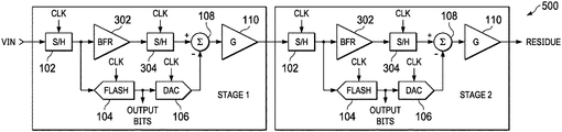
- FIG. 5 illustrates two example stages using the architecture of FIG. 3 .
- FIG. 6 shows another example of an architecture of two stage pipelined ADC.
- FIG. 7 shows a timing diagram applicable to the ADC stages of FIG. 6 .
- FIG. 8 shows an example implementation of at least some of the stages of the ADC of FIG. 6 .
- FIG. 9A shows an example of a logic circuit usable in the implementation of FIG. 8 .
- FIG. 9B illustrates the function performed by the logic circuit of FIG. 9A .
- FIG. 10 shows an example implementation of a comparator usable in flash converters usable in the example of FIG. 6 .
- FIG. 11 shows an example timing diagram pertaining to the comparator of FIG. 10 .
- FIG. 12 shows another example of a timing diagram pertain to the comparator of FIG. 10 .
- FIG. 13 shows an example implementation of a logic circuit usable to enable and disable a latch for the comparator of FIG. 10 .
- FIG. 14 shows an example implementation of a transceiver in which the ADC of FIG. 6 is usable.
- FIG. 1 shows an example of a single stage 100 of a pipelined ADC architecture.
- the single stage 100 includes a sample-and-hold (SH) 102 , a flash converter 104 , a digital-to-analog converter (DAC) 106 , a voltage subtractor 108 , and an amplifier 110 (with gain G).
- the analog input voltage is shown as VIN and is sampled and held by SH 102 .
- the sampled input voltage from SH 102 is provided to flash converter 104 , which converts the sampled input voltage to a digital representation.
- the flash converter 104 includes multiple comparators, and each comparator compares the sampled input voltage to a separate reference voltage.
- the output from flash converter 104 represents the n most significant bits of the digital representation of VIN.
- the flash converter 104 of this signal stage 100 has a resolution that is lower than the resolution of the overall pipelined ADC of which the stage 100 is a part.
- the overall resolution of the ADC may be, for example, 12 bits, while the resolution of stage 100 is 3 bits.
- Each stage of the ADC provides some of the digital bits of the final digital representation of VIN. As stage 100 is the first stage in the pipelined architecture, stage 100 generates the most significant n bits of the final digital representation of VIN. If the resolution of stage 100 is 3 bits, then stage 100 generates the 3 most significant bits.
- the flash converter 104 having a lower resolution than the overall ADC, produces a digital representation that is not necessarily the same as what the final digital representation of VIN would be from the combined efforts of all of the stages.
- the flash converter's output is converted back to an analog signal by DAC 106 .
- the DAC 106 in this example may be implemented as a capacitive DAC.
- the analog output from DAC 106 is then subtracted from the sampled VIN by voltage subtractor 108 .
- the difference signal from voltage subtractor 108 is then amplified by amplifier 110 to produce a residue, which is then provided to the next stage of the pipelined architecture.
- the next stage may be the same or similar to that shown in FIG. 1 and operates to generate the next set of bits of the digital representation of VIN.
- the pipelined architecture includes one or more stages such as that shown in FIG. 1 .
- the last stage of the ADC may only include a flash converter 104 to produce the one or more least significant bits of the digital representation of VIN.
- FIG. 1 illustrates a clock signal (CLK) provided to the SH 102 , flash converter 104 , and DAC 106 .
- CLK clock signal
- FIG. 2 illustrates a timing diagram for the operation of the single stage 100 of the pipelined ADC architecture. The clock period is shown as T.
- the SH 102 samples VIN ( 202 ).
- the flash converter 104 operates to convert the sampled input voltage to a digital representation.
- the DAC 106 converts the digital value from flash converter 106 to an analog equivalent and the amplifier 110 amplifies the difference signal from voltage subtractor 108 to generate the residue signal.
- the period T is smaller, and thus the amount of time to sample in the input and perform each of the flash conversion, the digital-to-analog conversion, and amplification becomes smaller.
- RF radio frequency
- the architecture shown in FIG. 1 becomes impractical.
- the comparators within the flash converter 104 may require, for example, 80 ps to compare the sampled input voltage to the respective reference voltages, which does not provide sufficient time for the DAC 106 and amplifier 110 .
- the example ADC stage 300 of FIG. 3 addresses the timing problem described above through the inclusion of buffer 302 , along with a second SH 304 .
- the buffer 302 operationally delays the sampled input voltage before reaching the voltage subtractor 108 to provide additional time for the flash converter 104 to convert the sampled input voltage from SH 102 to a digital representation.
- FIG. 4 shows a timing diagram corresponding to FIG. 3 .
- the input voltage VIN is sampled by SH 102 .
- the DAC 106 receives flash converter 104 's digital value of a previous sampled VIN and converts that digital value to an analog voltage.
- SH 304 samples the output of buffer 302 (which is a delayed version of the SH 102 's output). Also, in the same half cycle 403 , the flash converter 104 converts the sampled input voltage from the first half cycle 402 to a digital value. In the next half cycle 406 , amplifier 110 amplifies the difference signal from voltage subtractor 108 , while SH 102 again samples VIN.
- FIG. 5 shows two back-to-back stages—Stage 1 and Stage 2 —of a pipelined ADC.
- Stage 1 and Stage 2 includes the components described above regarding FIG. 3 .
- Stage 1 and Stage 2 both include a buffer 302 and two SHs 102 and 304 . While the buffers 302 provides sufficient time for the ADC to operate even at sample speeds in excess of 1 GSPS, the buffer 302 increases the overall power consumption of the ADC. Further, the buffers 302 and the extra SH 304 introduce additional noise into the ADC signal chain.
- FIG. 6 also shows an example of two stages—Stage 1 and Stage 2 —of a pipelined ADC 600 .
- the architecture of Stage 1 differs from the architecture of Stage 2 in this example.
- Stage 1 includes SHs 602 and 610 , a flash converter 604 , a DAC 606 (e.g., capacitive DAC), a buffer 608 , a voltage subtractor 612 , and an amplifier 614 (with gain G).
- the analog input voltage is shown as VIN and is sampled and held by SH 602 to produce a sampled value shown as VIN 1 .
- the sampled input voltage from SH 602 is provided to flash converter 604 , which converts the sampled input voltage to a digital representation.
- VIN 1 is also provided to, and buffered by, buffer 608 to produce buffer output signal VIN 2 .
- VIN 2 is then sampled and held by SH 610 .
- the flash converter 604 includes multiple comparators, and each comparator compares the sampled input voltage to a separate reference voltage.
- the flash converter 604 's output is converted back to an analog signal by DAC 606 .
- the analog output from DAC 606 is then subtracted from the sampled output from buffer 608 by voltage subtractor 608 .
- the difference signal from voltage subtractor 608 is then amplified by amplifier 610 to produce a residue 615 , which is then provided to Stage 2 of the pipelined architecture of FIG. 6 .
- Stage 2 of FIG. 6 includes SH 622 , a flash converter 624 , a DAC 626 (e.g., capacitive DAC), a voltage subtractor 632 , and an amplifier 634 (with gain G).
- the residue 615 from Stage 1 is sampled and held by SH 622 , and provided to voltage subtractor 632 .
- VIN 2 output signal from buffer 608 of Stage 1
- the flash converter 624 includes multiple comparators, and each comparator compares the sampled input voltage to a separate reference voltage.
- the flash converter 624 's output is converted back to an analog signal by DAC 626 .
- the analog output from DAC 626 is then subtracted from the sampled residue by voltage subtractor 632 .
- the difference signal from voltage subtractor 632 is then amplified by amplifier 634 to produce a residue 635 , which is then provided to a subsequent stage of the pipelined architecture.
- Stage 1 generates the n most significant bits of the digital representation of VIN
- Stage 2 generates the m next most significant bits of the digital representation of VIN.
- the values of n and m may be the same or different.
- both of Stages 1 and 2 of FIG. 5 include buffers 302 .
- the flash 104 in Stage 2 of FIG. 5 converts the sampled residue from Stage 1 to a digital representation.
- Stage 1 includes buffer 608 , but Stage 2 does not include a buffer.
- the input to flash converter 624 of Stage 2 is the output of buffer 608 of Stage 1 .
- the flash converter 624 of Stage 2 converts the sampled and buffered VIN from Stage 1 , rather than the residue signal from Stage 1 .
- the flash converter 624 is clocked using LATP 2 as well as a control signal 613 derived from the output signals generated by flash converter 604 .
- the clock signals to the flash converters 604 and 624 are shown as LATP 1 and LATP 2 , respectively. Additional stages may be included as well. Each subsequent stage may have the same architecture as Stage 2 .
- the flash converter of each subsequent Nth stage receives as an input the residue from N ⁇ 2 stage, and has its flash converter controlled by control signals derived from the output of the flash converter of the N ⁇ 1 stage.
- the flash converter of Stage 3 receives the residue from Stage 1 as an input.
- the output from the flash converter of Stage 2 is used to control the flash converter of Stage 3 .
- a final stage of the pipelined ADC may include a flash converter, but no DAC, voltage subtractor, nor amplifier.
- FIG. 7 shows an example timing diagram.
- the input voltage VIN is sampled by SH 602 of Stage 1 .
- the second SH 610 of Stage 1 samples the buffer 608 's output.
- the flash converter 604 of Stage 1 converts VIN 1 to a digital representation.
- the DAC 606 of Stage 1 converts the output from flash converter 604 generated during the previous half cycle 704 to an analog equivalent.
- amplifier 614 amplifies the difference signal from voltage subtractor 612 to residue 615 .
- the flash converter 624 of Stage 2 converts VIN 2 from buffer 608 to a digital representation.
- the DAC 626 of Stage 2 converts the output from flash converter 624 generated during the previous half cycle 706 to an analog equivalent, and amplifier 634 amplifies the difference signal from voltage subtractor 632 .
- FIG. 8 illustrates the comparators of flash converter 604 of Stage 1 , the comparators of flash converter 624 of Stage 2 , logic circuit 810 , multiplexer select circuit 820 , and multiplexer 830 . Any or all of the logic circuit 810 , multiplexer select circuit 820 , and multiplexer 830 may be part of flash converter 604 , or part of flash converter 624 , or separate from either flash converter.
- flash converter 604 of Stage 1 comprises a 3-bit converter to generate a 3-bit digital representation of VIN 1 .
- flash converter 604 includes eight comparators 841 - 848 . Each comparator includes a positive input, a negative input, and a comparator (COMP) output.
- COMP comparator
- the positive inputs for the comparators 841 - 848 are coupled to VIN 1 , and the negative inputs are coupled to separate reference voltages.
- the negative inputs of comparators 841 , 842 , 843 , 844 , 845 , 846 , 847 , and 848 are coupled to reference voltages Ref 1 , Ref 2 , Ref 3 , Ref 4 , Ref 5 , Ref 6 , Ref 7 , and Ref 8 , respectively.
- Comparator 841 asserts its output signal COMP 1 high when VIN 1 is greater than Ref 1 , and low otherwise.
- Comparator 842 asserts its output signal COMP 2 high when VIN 1 is greater than Ref 2 , and low otherwise.
- Comparator 843 asserts its output signal COMP 3 high when VIN 1 is greater than Ref 3 , and low otherwise.
- Comparator 844 asserts its output signal COMP 4 high when VIN 1 is greater than Ref 4 , and low otherwise.
- Comparator 845 asserts its output signal COMP 5 high when VIN 1 is greater than Ref 5 , and low otherwise.
- Comparator 846 asserts its output signal COMP 1 high when VIN 6 is greater than Ref 6 , and low otherwise.
- Comparator 847 asserts its output signal COMP 7 high when VIN 1 is greater than Ref 7 , and low otherwise.
- Comparator 848 asserts its output signal COMP 8 high when VIN 1 is greater than Ref 8 , and low otherwise.
- the comparators' output signals indicate the relative level of VIN 1 .
- COMP 1 through COMP 6 will be logic high, and COMP 7 and COMP 8 will be logic low, that is, COMP 1 through COMP 8 will be 11111100.
- the COMP 1 -COMP 8 signals comprise the digital value from flash converter 604 and can be converted to a 3-bit binary value, and provided to DAC 606 as described above.
- the COMP 1 -COMP 8 signals also are used to control the operation of flash converter 624 in Stage 2 .
- the Stage 2 flash converter 624 in this example comprises a 2-bit converter, and thus four comparators are used to generate the digital output value from flash converter 624 .
- the flash converter 104 of Stage 2 converted the sampled residue signal from Stage 1 to a digital representation.
- the input voltage range of flash converter 104 in Stage 2 is limited to the residue range, and only four comparators are included (assuming, for example, a 2-bit resolution for flash converter 104 of Stage 2 ).
- FIG. 5 the example of FIG. 5
- the flash converter 624 of Stage 2 converts buffered output signal VIN 2 to a digital presentation, and VIN 2 includes the full range of VIN.
- the reference voltages provided to the comparators of flash converter 624 increase in magnitude from comparator 861 to comparator 874 .
- Refb is greater than Refa
- Refc is greater than Refb, and so on.
- comparators 861 - 874 Only four comparators from among comparators 861 - 874 are used (assuming a 2-bit flash converter 624 resolution) as the digital value from flash converter 624 , and the COMP 1 -COMP 8 bits from flash converter 604 are used to cause the appropriate four comparators from flash converter 624 to be selected via multiplexer 830 .
- Logic circuit 810 and multiplexer select circuit 820 are used in this regard.
- Logic circuit 810 includes AND gates 851 - 857 .
- One input of each AND gate 851 - 857 is inverted, or a separate inverter can be provided for one of the AND gate inputs.
- Each AND gate determines the logical AND of one comparator 841 - 848 outputs and the inverted output of the next comparator output in sequence.
- AND gate 851 determines COMP 1 AND COMP 2 _BAR (where COMP 2 _BAR is the logical inverse of COMP 2 ) to produce select signal SEL 1 .
- AND gate 852 determines COMP 2 AND COMP 3 _BAR (where COMP 3 _BAR is the logical inverse of COMP 3 ) to produce select signal SEL 2 .
- AND gate 853 determines COMP 3 AND COMP 4 _BAR (where COMP 4 _BAR is the logical inverse of COMP 4 ) to produce select signal SEL 3 .
- AND gate 854 determines COMP 4 AND COMP 5 _BAR (where COMP 5 _BAR is the logical inverse of COMP 5 ) to produce select signal SEL 4 .
- AND gate 855 determines COMP 5 AND COMP 6 _BAR (where COMP 6 _BAR is the logical inverse of COMP 6 ) to produce select signal SEL 5 .
- AND gate 856 determines COMP 6 AND COMP 7 _BAR (where COMP 7 _BAR is the logical inverse of COMP 7 ) to produce select signal SEL 6 .
- AND gate 857 determines COMP 7 AND COMP 8 _BAR (where COMP 8 _BAR is the logical inverse of COMP 8 ) to produce select signal SEL 7 .
- the last select signal is SEL 8 and is the output signal COMP 8 from comparator 848 .
- a select signal SEL 1 -SEL 8 will only be a logic high when the non-inverted input is 1 and the other input is 0.
- SEL 6 will be a 1 when COMP 6 is a 1 and COMP 7 is a 0. Otherwise, each select signal is a logic 0.
- a select signal indicates the transition of the COMP signals from a 1 to a 0, which indicates that the voltage level of VIN 1 is between the reference voltages of the two comparators whose COMP outputs are coupled to the AND gate that produced the select signal that is a 1.
- SEL 6 will only be a 1 if VIN 1 is between Ref 6 and Ref 7 .
- Each select signal SEL 1 -SEL 8 is used to enable a particular set of comparators within the Stage 2 flash converter 624 .
- SEL 6 is used to enable comparators 863 - 866 .
- Select signal SEL 7 is used to enable comparators 867 - 870 , and SEL 8 is used to enable comparators 871 - 874 .
- Each of the other select signals also enable a given set of comparators within the flash converter 624 . The use of the select signals to enable/disable their corresponding set of comparators is discussed below regarding FIG. 13 .
- the outputs from comparators 861 - 874 of the flash converter 624 are couple to corresponding inputs of multiplexer 830 .
- Multiplexer select circuit 820 receives the COMP 1 :COMP 8 signals from the flash converter 604 and processes those signals to generate a multiplexer select signal 850 to cause the multiplexer 830 to select as its outputs 880 the particular four comparator outputs corresponding to the asserted select signal.
- the outputs of comparators 863 - 866 are coupled to the outputs 880 of multiplexer 830 as the digital output of flash converter 624 .
- the four bits from multiplexer 830 can be converted to a 2-bit binary value which is then provided to DAC 626 .
- one of the COMP 1 through COMP 8 bits is of the opposite polarity from what it should be.
- the COMP 1 :COMP 8 signals could have two 1-0 transitions (e.g., 11101000).
- a 1 to 0 transition between successive comparator output signals indicates that VIN 1 is between the reference voltages of the comparators 841 - 848 corresponding to 1 to 0 transition.
- the select signal from that AND gate 851 - 857 will be asserted to indicate the 1 to 0 transition. However, if the COMP 1 :COMP 8 signals includes two 1 to 0 transitions, two select signals SELx will be asserted high. This condition is referred to as a “bubble.” The select signal indicating the 1 to 0 transition closest to COMP 1 of comparator 841 having the smallest reference voltage Ref 1 should be selected.
- FIG. 9A shows example implementation of the multiplexer select circuit 820 .
- the multiplexer select circuit 820 includes multiple logic circuits 901 a , 901 b , 901 c , etc., each logic circuit 901 configured to receive four consecutive COMP signals from the comparators of the flash converter 604 .
- the inputs are designated A, B, C, and D.
- the D input is inverted as shown.
- Input A receives one comparator COMP 1 -COMP 8 signal.
- B receives the next consecutive COMP signal, C the next, and D the next.
- COMP 1 through COMP 4 of FIG. 8 are provided to inputs A through D, respectively, of logic circuit 901 a .
- COMP 2 -COMP 5 are similarly provided to inputs A through D of the next logic circuit 901 b , COMP 3 -COMP 6 provided to A through D of the next logic circuit 901 c , and so on.
- Each logic circuit comprises an AND gate 902 and an exclusive OR gate 910 .
- the exclusive OR gate 910 determines the exclusive OR of inputs B and C.
- the output of exclusive OR gate 910 is logically ANDed with A and D.
- the output signal from each logic circuit 901 is a multiplexer select signal (MUX SEL) and collectively represent the multiplexer select signal 850 shown in FIG. 8 .
- a MUX SEL signal is only asserted high (1) when both A is a logic 1, D is a logic 0, and the exclusive OR gate generates a logic 1 (which only happens when B and C are of opposite polarity).
- the logic implementation of logic circuits 901 means that, as shown in FIG. 9B , the MUX SEL will only be a 1 when A-D are either (a) 1-1-0-0, or (b) 1-0-1-0.
- FIG. 10 shows an example implementation of a comparator usable for the flash converter 624 of Stage 2 , but usable as well for the flash converter of Stage 1 or any other stage of the pipelined ADC.
- the comparator in the example of FIG. 10 includes a pre-amplifier (pre-amp) 1010 coupled to a latch 1030 .
- the pre-amp 1010 in this example includes transistors M 1 , M 2 , M 3 , M 4 , M 5 , and M 6 , resistors R 1 and R 2 , and current source device 11 .
- M 1 -M 4 comprise n-type metal oxide semiconductor field effect transistors (NMOS) in this example, and M 5 and M 6 comprise p-type metal oxide semiconductor field effect transistors (PMOS).
- NMOS n-type metal oxide semiconductor field effect transistors
- PMOS p-type metal oxide semiconductor field effect transistors
- the sources of M 1 and M 2 are connected to the current source device 11 .
- the drains of M 1 and M 2 are connected to the sources of M 3 and M 4 , respectively, and the drains of M 3 and M 4 are connected to R 1 and R 2 , respectively.
- the drains of M 5 and M 6 are connected to the opposing terminals of R 1 and R 2 , and the sources of M 5 an M 6 are connected to a supply voltage node (VDD).
- the input voltages to be compared are provided to the gates of M 1 and M 2 .
- VIN 2 is provided to the gate of M 1
- REFx is provided to the gate of M 2 .
- the pre-amp 1010 can be enabled or disabled via the clock signal LATP, which controls the gates of M 5 and M 6 .
- a low level of LATP (e.g., more than the threshold voltage of M 5 and M 6 below VDD) turns on M 5 and M 6
- a high level (within a threshold voltage of VDD) turns of M 5 and M 6
- the logical inverse of LATP (LATP_BAR) controls the gates of M 3 and M 4 .
- the output from the pre-amp 1010 is taken from nodes N 1 (node interconnecting M 3 and R 1 ) and N 2 (node interconnecting M 4 and R 2 ).
- the pre-amp 1010 comprises two current branches. One branch comprises M 5 , R 1 , M 3 , and M 1 . The other branch comprises M 6 , R 2 , M 4 , and M 2 .
- current source device 11 causes current to flow through one of the branches or the other of the pre-amp based on the relative size of the VIN 2 and REFx. If VIN 2 is greater than REFX, M 1 turns on “harder” than M 2 , and more of the current source device 11 current flows from VDD and through M 5 , R 1 , M 3 , and M 1 to ground. In this state, the voltage on N 2 is greater than the voltage on N 1 .
- the latch 1030 in the example of FIG. 10 includes M 7 , M 8 , M 9 , M 10 , M 11 , M 12 , and M 13 with M 7 -M 10 configured as two pairs of cross-coupled transistors.
- M 7 -M 9 comprise NMOS transistors.
- the sources of M 7 and M 8 connect to the drain of M 11
- the drains of M 7 and M 8 connect to the drains of M 9 and M 10 , respectively.
- the drains of M 7 and M 9 also connect to the gates of M 8 and M 10
- the drains of M 8 and M 10 connect to the gates of M 7 and M 9 .
- Node N 3 is the node interconnecting the drains of M 7 and M 9
- node N 4 is the node interconnecting the drains of M 8 and M 10
- the COMP output of the latch 1030 is taken as the voltage on N 4
- M 12 and M 13 can be turned on via a reset signal (RST) to reset the pull both nodes N 3 and N 4 high thereby resetting the latch's COMP output to a 1.
- Nodes N 1 and N 2 from the pre-amp 1010 connect to nodes N 3 and N 4 , respectively, of the latch 1030 .
- the latch 1030 regenerates the voltages from N 1 and N 2 onto N 3 and N 4 .
- the latch 1030 holds the voltages on N 3 and N 4 even if the pre-amp 1010 no longer actively drives the voltages on N 1 and N 2 .
- N 4 is greater than N 3
- M 7 turns on thereby reinforcing the low voltage on N 3 .
- N 3 being low, M 10 is turned on thereby reinforcing the higher voltage on N 4 .
- FIG. 11 shows an example timing diagram for the operation of the comparator of FIG. 10 .
- the comparators of flash converter 604 of Stage 1 regenerate to produce their comparator output data.
- the comparators of flash converter 604 have had enough time to regenerate and their output data has settled.
- the pre-amps 1010 of the comparators of Stage 2 's flash converter 624 are enabled (LATP asserted low, and LATP_BAR asserted high).
- the latches 1030 of the flash converter 624 also regenerate to produce their COMP output data.
- the flash converter 624 begins regeneration within its latches 1030 synchronous with the pre-amps 1010 being enabled.
- FIG. 12 shows a timing diagram similar to that of FIG. 11 , but illustrating a situation in which the data from the flash converter 604 does not settle until 1105 meaning that the data from flash converter 604 is not available until 1105 (which is within the second half cycle 1104 ).
- VIN 2 Due to the timing of the SH 602 within Stage 1 , VIN 2 needs to be sampled by the pre-amp 1010 of flash converter 624 within Stage 2 by the end of the first half cycle 1102 (point 1107 ); else VIN 2 will have changed.
- the pre-amps 1010 should be enabled to use VIN 2 and the reference voltage to generate the voltages on N 1 and N 2 during the first half cycle 1101 , but then be disabled at 1107 to avoid processing a new level of VIN 2 .
- the latches 1030 within the flash converter 624 should not be enabled, however, until the data from the flash converter 604 have settled at 1110 ; else the control of the logic circuit 810 , multiplexer select circuit 820 , and multiplexer 830 (which uses the COMP signals from flash converter 604 ) may not be correct.
- FIG. 13 shows an example of the generation of LATP_ASYNCH to control the latches 1030 .
- An AND gate 1302 logically ANDs together LATP_BAR with the select signal (SELx) used to select the subgroup of comparators 861 - 874 within flash converter 624 .
- SEL select signal
- SEL is asserted high when consecutive COMP signals from corresponding comparators 841 - 848 are 1 followed by 0.
- the select signal is used asynchronously gate off LATP_BAR until a valid 1 to 0 transition is detected from among the comparators 841 - 848 .
- FIG. 14 provides an example of a transceiver 1400 comprising one or more transmitters 1402 , a feedback circuit 1404 , and one or more receivers 1406 .
- the feedback circuit 1404 includes at least one pipelined ADC 1410 such as that described herein.
- the feedback circuit 1404 receives the transmitter's output signal and processes the output signal to measure the non-linearity in the transmit signal path. The measured non-linearity is then used by the feedback circuit 1404 to correct the transmit path on the fly. The non-linearity correction is particular useful as an amplifier within the transmitter 1402 may have a non-linear performance.
- the ADC 1410 is used to aide in measuring the non-linearity of the transmit signal path.
- the ADC 1410 converts the transmitter's output signal to a digital representation for further processing within the feedback circuit 1404 .
- the feedback circuit 1404 can be used to calibrate each of multiple transmitters 1402 .
- Couple means either an indirect or direct wired or wireless connection.
- a first device couples to a second device, that connection may be through a direct connection or through an indirect connection via other devices and connections.
- the recitation “based on” means “based at least in part on.” Therefore, if X is based on Y, X may be a function of Y and any number of other factors.
Abstract
Description
Claims (18)
Applications Claiming Priority (2)
| Application Number | Priority Date | Filing Date | Title |
|---|---|---|---|
| IN201841010558 | 2018-03-22 | ||
| IN201841010558 | 2018-03-22 |
Publications (2)
| Publication Number | Publication Date |
|---|---|
| US20190296758A1 US20190296758A1 (en) | 2019-09-26 |
| US10644714B2 true US10644714B2 (en) | 2020-05-05 |
Family
ID=67985711
Family Applications (1)
| Application Number | Title | Priority Date | Filing Date |
|---|---|---|---|
| US16/358,456 Active US10644714B2 (en) | 2018-03-22 | 2019-03-19 | Pipelined analog-to-digital converter |
Country Status (1)
| Country | Link |
|---|---|
| US (1) | US10644714B2 (en) |
Citations (4)
| Publication number | Priority date | Publication date | Assignee | Title |
|---|---|---|---|---|
| US4763107A (en) * | 1985-08-23 | 1988-08-09 | Burr-Brown Corporation | Subranging analog-to-digital converter with multiplexed input amplifier isolation circuit between subtraction node and LSB encoder |
| US20060077086A1 (en) * | 2004-10-11 | 2006-04-13 | Cringean Andrew J | Analogue to digital converter |
| US20120319879A1 (en) * | 2011-06-14 | 2012-12-20 | Analog Devices, Inc. | Method for modifying the lms algorithm to reduce the effect of correlated perturbations |
| US20130106630A1 (en) * | 2011-11-02 | 2013-05-02 | Semtech Corporation | Successive approximation analog-to-digital conversion |
-
2019
- 2019-03-19 US US16/358,456 patent/US10644714B2/en active Active
Patent Citations (4)
| Publication number | Priority date | Publication date | Assignee | Title |
|---|---|---|---|---|
| US4763107A (en) * | 1985-08-23 | 1988-08-09 | Burr-Brown Corporation | Subranging analog-to-digital converter with multiplexed input amplifier isolation circuit between subtraction node and LSB encoder |
| US20060077086A1 (en) * | 2004-10-11 | 2006-04-13 | Cringean Andrew J | Analogue to digital converter |
| US20120319879A1 (en) * | 2011-06-14 | 2012-12-20 | Analog Devices, Inc. | Method for modifying the lms algorithm to reduce the effect of correlated perturbations |
| US20130106630A1 (en) * | 2011-11-02 | 2013-05-02 | Semtech Corporation | Successive approximation analog-to-digital conversion |
Also Published As
| Publication number | Publication date |
|---|---|
| US20190296758A1 (en) | 2019-09-26 |
Similar Documents
| Publication | Publication Date | Title |
|---|---|---|
| US11316505B2 (en) | Delay based comparator | |
| US7557746B1 (en) | Time domain interpolation scheme for flash A/D converters | |
| US8957794B2 (en) | A/D converter and method for calibrating the same | |
| US8421664B2 (en) | Analog-to-digital converter | |
| US9467160B2 (en) | Flash ADC with interpolators | |
| US7576677B2 (en) | Pipeline A/D converter converting analog signal to digital signal | |
| US20160254821A1 (en) | Successive Approximation Register-based Analog-to-Digital Converter with Increased Time Frame for Digital-to-Analog Capacitor Settling | |
| US7224306B2 (en) | Analog-to-digital converter in which settling time of amplifier circuit is reduced | |
| US7986257B2 (en) | Comparator circuit and analog digital converter having the same | |
| US9654126B2 (en) | Systems and methods for providing a pipelined analog-to-digital converter | |
| US7847720B2 (en) | Pipelined analog-to-digital converter | |
| US7768432B2 (en) | Analog-to-digital conversion devices and analog-to-digital conversion stages thereof | |
| CN110401447B (en) | MDAC type time domain ADC structure without operational amplifier | |
| US9013344B2 (en) | High speed dynamic comparator | |
| US9357151B1 (en) | Shared counter circuit with low-voltage signal output for a column-parallel single slope ADC | |
| US10476456B2 (en) | Comparator having a high-speed amplifier and a low-noise amplifier | |
| US6504500B1 (en) | A/D converter and A/D converting method | |
| US10644714B2 (en) | Pipelined analog-to-digital converter | |
| US7535399B2 (en) | Reference voltage shifting technique for optimizing SNR performance in pipeline ADCs with respect to input signal | |
| WO2020090434A1 (en) | Analog-digital converter | |
| JP2017046058A (en) | AD converter, analog front end, and sensor system | |
| JP4858962B2 (en) | Semiconductor integrated circuit device | |
| US20100277357A1 (en) | Analog-to-digital converter | |
| JP7439930B2 (en) | analog to digital converter | |
| Huang et al. | A 5-bit 1 Gsample/s two-stage ADC with a new flash folded architecture |
Legal Events
| Date | Code | Title | Description |
|---|---|---|---|
| AS | Assignment |
Owner name: TEXAS INSTRUMENTS INCORPORATED, TEXAS Free format text: ASSIGNMENT OF ASSIGNORS INTEREST;ASSIGNORS:MOHAN, ARUN;SHRIVASTAVA, NEERAJ;REEL/FRAME:048641/0267 Effective date: 20190318 |
|
| FEPP | Fee payment procedure |
Free format text: ENTITY STATUS SET TO UNDISCOUNTED (ORIGINAL EVENT CODE: BIG.); ENTITY STATUS OF PATENT OWNER: LARGE ENTITY |
|
| STPP | Information on status: patent application and granting procedure in general |
Free format text: NON FINAL ACTION MAILED |
|
| STPP | Information on status: patent application and granting procedure in general |
Free format text: RESPONSE TO NON-FINAL OFFICE ACTION ENTERED AND FORWARDED TO EXAMINER |
|
| STPP | Information on status: patent application and granting procedure in general |
Free format text: NOTICE OF ALLOWANCE MAILED -- APPLICATION RECEIVED IN OFFICE OF PUBLICATIONS |
|
| STCF | Information on status: patent grant |
Free format text: PATENTED CASE |
|
| MAFP | Maintenance fee payment |
Free format text: PAYMENT OF MAINTENANCE FEE, 4TH YEAR, LARGE ENTITY (ORIGINAL EVENT CODE: M1551); ENTITY STATUS OF PATENT OWNER: LARGE ENTITY Year of fee payment: 4 |