US10643013B2 - Tie-high and tie-low circuits - Google Patents
Tie-high and tie-low circuits Download PDFInfo
- Publication number
- US10643013B2 US10643013B2 US15/985,007 US201815985007A US10643013B2 US 10643013 B2 US10643013 B2 US 10643013B2 US 201815985007 A US201815985007 A US 201815985007A US 10643013 B2 US10643013 B2 US 10643013B2
- Authority
- US
- United States
- Prior art keywords
- transistor
- tie
- drain
- circuit
- pmos transistor
- Prior art date
- Legal status (The legal status is an assumption and is not a legal conclusion. Google has not performed a legal analysis and makes no representation as to the accuracy of the status listed.)
- Active, expires
Links
Images


Classifications
-
- H—ELECTRICITY
- H03—ELECTRONIC CIRCUITRY
- H03K—PULSE TECHNIQUE
- H03K3/00—Circuits for generating electric pulses; Monostable, bistable or multistable circuits
- H03K3/02—Generators characterised by the type of circuit or by the means used for producing pulses
- H03K3/353—Generators characterised by the type of circuit or by the means used for producing pulses by the use, as active elements, of field-effect transistors with internal or external positive feedback
- H03K3/356—Bistable circuits
- H03K3/356104—Bistable circuits using complementary field-effect transistors
- H03K3/356182—Bistable circuits using complementary field-effect transistors with additional means for controlling the main nodes
-
- G—PHYSICS
- G06—COMPUTING OR CALCULATING; COUNTING
- G06F—ELECTRIC DIGITAL DATA PROCESSING
- G06F30/00—Computer-aided design [CAD]
- G06F30/30—Circuit design
- G06F30/39—Circuit design at the physical level
-
- H01L27/0251—
-
- H01L27/0266—
-
- H01L27/0288—
-
- H01L27/11807—
-
- H—ELECTRICITY
- H03—ELECTRONIC CIRCUITRY
- H03K—PULSE TECHNIQUE
- H03K19/00—Logic circuits, i.e. having at least two inputs acting on one output; Inverting circuits
- H03K19/20—Logic circuits, i.e. having at least two inputs acting on one output; Inverting circuits characterised by logic function, e.g. AND, OR, NOR, NOT circuits
-
- H—ELECTRICITY
- H10—SEMICONDUCTOR DEVICES; ELECTRIC SOLID-STATE DEVICES NOT OTHERWISE PROVIDED FOR
- H10D—INORGANIC ELECTRIC SEMICONDUCTOR DEVICES
- H10D84/00—Integrated devices formed in or on semiconductor substrates that comprise only semiconducting layers, e.g. on Si wafers or on GaAs-on-Si wafers
- H10D84/90—Masterslice integrated circuits
- H10D84/903—Masterslice integrated circuits comprising field effect technology
- H10D84/907—CMOS gate arrays
-
- H—ELECTRICITY
- H10—SEMICONDUCTOR DEVICES; ELECTRIC SOLID-STATE DEVICES NOT OTHERWISE PROVIDED FOR
- H10D—INORGANIC ELECTRIC SEMICONDUCTOR DEVICES
- H10D89/00—Aspects of integrated devices not covered by groups H10D84/00 - H10D88/00
- H10D89/60—Integrated devices comprising arrangements for electrical or thermal protection, e.g. protection circuits against electrostatic discharge [ESD]
- H10D89/601—Integrated devices comprising arrangements for electrical or thermal protection, e.g. protection circuits against electrostatic discharge [ESD] for devices having insulated gate electrodes, e.g. for IGFETs or IGBTs
- H10D89/811—Integrated devices comprising arrangements for electrical or thermal protection, e.g. protection circuits against electrostatic discharge [ESD] for devices having insulated gate electrodes, e.g. for IGFETs or IGBTs using FETs as protective elements
-
- H—ELECTRICITY
- H10—SEMICONDUCTOR DEVICES; ELECTRIC SOLID-STATE DEVICES NOT OTHERWISE PROVIDED FOR
- H10D—INORGANIC ELECTRIC SEMICONDUCTOR DEVICES
- H10D89/00—Aspects of integrated devices not covered by groups H10D84/00 - H10D88/00
- H10D89/60—Integrated devices comprising arrangements for electrical or thermal protection, e.g. protection circuits against electrostatic discharge [ESD]
- H10D89/601—Integrated devices comprising arrangements for electrical or thermal protection, e.g. protection circuits against electrostatic discharge [ESD] for devices having insulated gate electrodes, e.g. for IGFETs or IGBTs
- H10D89/911—Integrated devices comprising arrangements for electrical or thermal protection, e.g. protection circuits against electrostatic discharge [ESD] for devices having insulated gate electrodes, e.g. for IGFETs or IGBTs using passive elements as protective elements
Definitions
- the following description relates to tie-high and tie-low circuits. More particularly, the following description relates to tie-high and tie-low circuits capable of functioning as a decoupling capacitor.
- a first step to designing an application specific Integrated circuit (ASIC) chip is to describe logic functions of the circuit to be implemented in the chip in a VHSIC hardware description language (VHDL) or a Verilog, which is a hardware description language.
- VHDL VHSIC hardware description language
- Verilog Verilog
- the code described in this language is subjected to a process called logic synthesis, which is mapped to a combination of standard cells performing basic logic functions. It may be necessary to fix an input of the standard cell to high or low due to a logic function. In this case, when a power node or a ground node is directly connected to an input of a gate of the standard cell via a metal, the input of the gate of the standard cell becomes vulnerable to an electrostatic discharge (ESD) signal.
- ESD electrostatic discharge
- TIEHI/TIELO tie-high/tie-low cells corresponding to cells whose an output signal is designed to have a power voltage level or a ground voltage level.
- TIEHI/TIELO tie-high/tie-low
- a tie-high circuit includes: a p-type metal-oxide-semiconductor (PMOS) transistor connected to a power rail in a standard cell library; and a decoupling capacitor connected to a ground rail in the standard cell library and the PMOS transistor wherein the decoupling capacitor comprises an n-type metal-oxide-semiconductor (NMOS) transistor having a source and a drain, either one of the source and the drain of the NMOS transistor being connected to the ground rail via an active resistor.
- PMOS p-type metal-oxide-semiconductor
- NMOS n-type metal-oxide-semiconductor
- the either one of the source and the drain of the NMOS transistor may be connected to a gate of the PMOS transistor.
- a gate of the NMOS transistor may be connected to a drain of the PMOS transistor, and an output of the tie-high circuit may be provided at the drain of the PMOS transistor.
- a source of the PMOS transistor may be connected to the power rail.
- the supply voltage (VDD) may be divided according to a ratio of an on resistance of the PMOS transistor to an effective resistance of the NMOS transistor so that the output of the tie-high circuit is provided at the drain of the PMOS transistor.
- a tie-low circuit in another general aspect, includes: an n-type metal-oxide-semiconductor (NMOS) transistor connected to a ground rail in a standard cell library; and a decoupling capacitor connected to a power rail in the standard cell library and the NMOS transistor, wherein the decoupling capacitor comprises a p-type metal-oxide-semiconductor (PMOS) transistor having a source and a drain, either one of the source and the drain of the PMOS transistor being connected to the power rail via an active resistor.
- NMOS n-type metal-oxide-semiconductor
- PMOS p-type metal-oxide-semiconductor
- the either one of the source and the drain of the PMOS transistor may be connected to a gate of the NMOS transistor.
- a gate of the PMOS transistor may be connected to a drain of the NMOS transistor, and an output of the tie-low circuit may be provided at the drain of the NMOS transistor.
- a source of the NMOS transistor may be connected to the ground rail.
- the supply voltage (VDD) may be divided according to a ratio of an effective resistance of the PMOS transistor to an on resistance of the NMOS transistor so that the output of the tie-low circuit is provided at the drain of the NMOS transistor.
- a tie-high circuit in a standard cell includes a first transistor and a decoupling capacitor.
- the first transistor is connected to a power rail.
- the decoupling capacitor is connected to a ground rail and the first transistor, and includes a second transistor having either one of a source and a drain of the second transistor being connected to the ground rail via an active resistor.
- the first transistor may be a p-type metal-oxide-semiconductor (PMOS) transistor and the second transistor may be an n-type metal-oxide-semiconductor (NMOS) transistor.
- PMOS metal-oxide-semiconductor
- NMOS n-type metal-oxide-semiconductor
- Either one of the source and the drain of the NMOS transistor may be connected to a gate of the PMOS transistor.
- a gate of the NMOS transistor may be connected to a drain of the PMOS transistor, and an output of the tie-high circuit may be provided at the drain of the PMOS transistor.
- a source of the PMOS transistor may be connected to the power rail.
- the VDD may be divided according to a ratio of an on resistance of the PMOS transistor to an effective resistance of the NMOS transistor so that the output of the tie-high circuit is provided at the drain of the PMOS transistor.
- FIG. 1 is a view illustrating a structure of a tie-high circuit according to an embodiment.
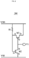
- FIG. 2 is a view illustrating a structure of a tie-low circuit according to an embodiment.
- FIG. 3A is a view illustrating an embodiment of a waveform of an electrostatic discharge (ESD) signal.
- ESD electrostatic discharge
- FIG. 3B is a view illustrating a result of performing an ESD simulation on the tie-high circuit according to an embodiment and a conventional tie-high circuit, where the conventional tie-high circuit is structured such that a source of an NMOS transistor is connected to a ground rail and a gate and drain of the NMOS transistor are connected to a gate of a PMOS transistor whose source is connected to a power rail and whose drain provides an output signal.
- FIG. 4A is a view illustrating a waveform of the ESD signal according to another embodiment.
- FIG. 4B is a view illustrating a result of performing the ESD simulation on the tie-low circuit according to an embodiment and a conventional tie-low circuit, where the conventional tie-low circuit is structured such that a source of a PMOS transistor is connected to a power rail and a gate and drain of the PMOS transistor are connected to a gate of an NMOS transistor whose source is connected to a power rail and whose drain provides an output signal.
- Embodiments disclosed herein are directed to tie-high and tie-low circuits capable of functioning as a decoupling capacitor.
- Embodiments of the disclosed tie-high circuit have a simplified structure in which a PMOS transistor used for the pull-up purpose is connected to a MOS capacitor.
- Embodiments of the disclosed tie-low circuit have a simplified structure in which an NMOS transistor used for the pull-down purpose is connected to a MOS capacitor.
- first,” “second,” and “third” may be used herein to describe various members, components, regions, layers, or sections, these members, components, regions, layers, or sections are not to be limited by these terms. Rather, these terms are only used to distinguish one member, component, region, layer, or section from another member, component, region, layer, or section. Thus, a first member, component, region, layer, or section referred to in examples described herein may also be referred to as a second member, component, region, layer, or section without departing from the teachings of the examples.
- spatially relative terms such as “above,” “upper,” “below,” and “lower” may be used herein for ease of description to describe one element's relationship to another element as shown in the figures. Such spatially relative terms are intended to encompass different orientations of the device in use or operation in addition to the orientation depicted in the figures. For example, if the device in the figures is turned over, an element described as being “above” or “upper” relative to another element will then be “below” or “lower” relative to the other element. Thus, the term “above” encompasses both the above and below orientations depending on the spatial orientation of the device.
- the device may also be oriented in other ways (for example, rotated 90 degrees or at other orientations), and the spatially relative terms used herein are to be interpreted accordingly.
- FIG. 1 is a view illustrating a structure of a tie-high circuit according to an embodiment.
- a tie-high circuit 100 may be disposed adjacent to standard cells that need to fix the input high in a standard cell library.
- the tie-high circuit 100 includes a p-type metal-oxide-semiconductor (PMOS) transistor M 0 that performs a pull-up function and an n-type metal-oxide-semiconductor (NMOS) transistor M 1 that serves as a decoupling capacitor.
- PMOS metal-oxide-semiconductor
- NMOS n-type metal-oxide-semiconductor
- a drain of the NMOS transistor M 1 is connected to a ground rail to which a ground voltage VSS is applied in the standard cell library, and a source of the NMOS transistor M 1 is connected to a gate of the PMOS transistor M 0 as well as the ground rail via an active resistor R 0 .
- the source of the NMOS transistor M 1 may be connected to the ground rail, and the drain of the NMOS transistor M 1 may connected to the gate of the PMOS transistor M 0 as well as the ground rail via the active resistor R 0 .
- the gate of the NMOS transistor M 1 may be connected to the drain of the PMOS transistor M 0 .
- An output terminal Y 0 of the tie-high circuit 100 has a ground potential in a state that a power voltage is not applied.
- a voltage to the tie-high circuit 100 is ramped up, and a voltage difference occurs between the gate and the source of the PMOS transistor M 0 .
- the PMOS transistor M 0 is turned on so that an output signal having substantially the same magnitude as the supply voltage VDD is output via the output terminal Y 0 .
- the NMOS transistor M 1 Since the gate of the NMOS transistor M 1 is connected to the drain of the PMOS transistor M 0 , that is, the output terminal Y 0 , the NMOS transistor M 1 is also turned on so that the NMOS transistor M 1 operates as a MOS capacitor. Since the gate of the PMOS transistor M 0 is connected to the ground rail via the active resistor R 0 connected to the source of the NMOS transistor M 1 , the input resistance of the gate of the PMOS transistor M 0 can be increased. Thus, the gate of the PMOS transistor M 0 can be protected from an electrostatic discharge (ESD) signal that may be caused from the ground rail.
- ESD electrostatic discharge
- the active resistor R 0 provided by an active region may have a resistance value of about 30-40 times a resistance value of a metal.
- a capacitance between the supply voltage and the ground can be increased, thereby enhancing the noise reduction effect in a supply node.
- the NMOS transistor M 1 operates as the MOS capacitor, a leakage current of about several pA flows through the NMOS transistor M 1 .
- the supply voltage VDD is divided according to a ratio of an on resistance Ron of the PMOS transistor M 0 to an effective resistance Reff of the NMOS transistor M 1 so that the supply voltage VDD is provided as an output signal in the output terminal Y 0 . Since the effective resistance Reff of the NMOS transistor M 1 is considerably larger than the on resistance Ron of the PMOS transistor M 0 , a voltage having substantially the same magnitude as the supply voltage VDD is applied via the output terminal Y 0 .
- FIG. 2 is a view illustrating a structure of a tie-low circuit according to an embodiment.
- a tie-low circuit 200 may be disposed adjacent to standard cells that need to hold an input low in the standard cell library.
- the tie-low circuit 200 includes an NMOS transistor M 2 that performs a pull-down function and a PMOS transistor M 3 that serves as the decoupling capacitor.
- a source of the NMOS transistor M 2 is connected to the ground rail, and a drain of the NMOS transistor M 2 is connected to an output terminal Y 1 .
- a drain of the PMOS transistor M 3 is connected to the power rail, and a source of the PMOS transistor M 3 is connected to a gate of the NMOS transistor M 2 as well as the power rail via an active resistor R 1 .
- the source of the PMOS transistor M 3 may connected to the power rail, and the drain of PMOS transistor M 3 may be connected to the gate of the NMOS transistor M 2 as well as the power rail via the active resistor R 1 .
- a gate of the PMOS transistor M 3 may be connected to the drain of the NMOS transistor M 2 .
- the output terminal Y 1 of the tie-low circuit 200 has a ground potential in a state that the initial power is not applied.
- a voltage to the tie-low circuit 200 is ramped up, and a voltage difference occurs between the gate and the source of the NMOS transistor M 2 .
- the NMOS transistor M 2 is turned on so that an output signal having substantially the same magnitude as the ground voltage VSS is output via the output terminal Y 1 .
- the PMOS transistor M 3 Since the gate of the PMOS transistor M 3 is connected to the drain of the NMOS transistor M 2 , that is, the output terminal Y 1 , the PMOS transistor M 3 is also turned on so that the PMOS transistor M 3 operates as the MOS capacitor. Since the gate of the NMOS transistor M 2 is connected to the power rail via the active resistor R 1 connected to the source of the PMOS transistor M 3 , an input resistance of the gate of the NMOS transistor M 2 can be increased. Thus, the gate of the NMOS transistor M 2 can be protected from the ESD signal.
- the active resistor R 1 provided by the active region may have a resistance value of about 30-40 times the resistance value of the metal.
- the capacitance between the supply voltage VDD and the ground can be increased, thereby enhancing the noise reduction effect in the supply node.
- the PMOS transistor M 3 operates as the MOS capacitor, a leakage current of about several pA flows through the PMOS transistor M 3 .
- the supply voltage VDD is divided according to a ratio of an effective resistance Reff of the PMOS transistor M 3 to an on resistance Ron of the NMOS transistor M 2 so that the supply voltage VDD is provided as an output signal in the output terminal Y 1 . Since the effective resistance Reff of the PMOS transistor M 3 is considerably larger than the on resistance Ron of the NMOS transistor M 2 , a voltage having substantially the same magnitude as the ground voltage VSS is applied via the output terminal Y 1 .
- FIG. 3A is a view illustrating an embodiment of a waveform of the ESD signal.
- FIG. 3B is a view illustrating a result of performing an ESD simulation on the tie-high circuit according to an embodiment and a conventional tie-high circuit, where the conventional tie-high circuit is structured such that a source of an NMOS transistor is connected to a ground rail and a gate and drain of the NMOS transistor are connected to a gate of a PMOS transistor whose source is connected to a power rail and whose drain provides an output signal.
- FIG. 3B shows a waveform of a voltage which is inputted to the gate of the PMOS transistor M 0 when the ESD signal shown in FIG. 3A flows into the tie-high circuit 100 according to an embodiment via the ground rail, and a waveform of a voltage which is inputted to the gate of the PMOS transistor when the ESD signal shown in FIG. 3A flows into the conventional tie-high circuit via the ground rail, as a solid line and a dotted line, respectively.
- the voltage inputted to the gate of the PMOS transistor M 0 has a magnitude of about ⁇ 5 V, but is gradually discharged over time and becomes close or asymptotic to a magnitude of about 0V.
- the voltage inputted to the gate of the PMOS transistor is about ⁇ 4.6 V, but is gradually discharged over time and becomes close to a magnitude of about ⁇ 0.6 V.
- the voltage inputted to the gate of the PMOS transistor M 0 of the tie-high circuit 100 has a magnitude of about 85% smaller than the voltage inputted to the gate of the PMOS transistor of the conventional tie-high circuit with respect to the absolute value.
- FIG. 4A is a view illustrating a waveform of the ESD signal according to another embodiment.
- FIG. 4B is a view illustrating a result of performing the ESD simulation on the tie-low circuit according to an embodiment and a conventional tie-low circuit, where the conventional tie-low circuit is structured such that a source of a PMOS transistor is connected to a power rail and a gate and drain of the PMOS transistor are connected to a gate of an NMOS transistor whose source is connected to a power rail and whose drain provides an output signal.
- FIG. 4B shows a waveform of a voltage which is inputted to the gate of the NMOS transistor M 2 when the ESD signal shown in FIG. 4A flows into the tie-low circuit 200 according to an embodiment via the power rail, and a waveform of a voltage which is inputted to the gate of the NMOS transistor when the ESD signal shown in FIG. 4A flows into the conventional tie-low circuit via the power rail, as a solid line and a dotted line, respectively.
- the voltage inputted to the gate of the NMOS transistor M 2 has a magnitude of about 5 V, but is gradually discharged over time and becomes close or asymptotic to a magnitude of about 0V.
- the voltage inputted to the gate of the NMOS transistor has about 4.6 V, but is gradually discharged over time and becomes close to a magnitude of about 0.6 V.
- the voltage inputted to the gate of the NMOS transistor M 2 of the tie-low circuit 200 has a magnitude of about 84% smaller than the voltage inputted to the gate of the NMOS transistor of the conventional tie-low circuit with respect to the absolute value.
- the arrangement of the illustrated components may vary depending on an environment or requirements to be implemented. For example, some of the components may be omitted or several components may be integrated and implemented together. In addition, the arrangement order of some of the components can be changed.
Landscapes
- Engineering & Computer Science (AREA)
- Computer Hardware Design (AREA)
- Physics & Mathematics (AREA)
- General Engineering & Computer Science (AREA)
- Theoretical Computer Science (AREA)
- Computing Systems (AREA)
- Mathematical Physics (AREA)
- Evolutionary Computation (AREA)
- Geometry (AREA)
- General Physics & Mathematics (AREA)
- Semiconductor Integrated Circuits (AREA)
Abstract
Description
Claims (16)
Applications Claiming Priority (2)
| Application Number | Priority Date | Filing Date | Title |
|---|---|---|---|
| KR1020170085900A KR102101537B1 (en) | 2017-07-06 | 2017-07-06 | Tie-High/Tie-Low Circuit |
| KR10-2017-0085900 | 2017-07-06 |
Publications (2)
| Publication Number | Publication Date |
|---|---|
| US20190012419A1 US20190012419A1 (en) | 2019-01-10 |
| US10643013B2 true US10643013B2 (en) | 2020-05-05 |
Family
ID=64903238
Family Applications (1)
| Application Number | Title | Priority Date | Filing Date |
|---|---|---|---|
| US15/985,007 Active 2038-05-24 US10643013B2 (en) | 2017-07-06 | 2018-05-21 | Tie-high and tie-low circuits |
Country Status (2)
| Country | Link |
|---|---|
| US (1) | US10643013B2 (en) |
| KR (1) | KR102101537B1 (en) |
Families Citing this family (2)
| Publication number | Priority date | Publication date | Assignee | Title |
|---|---|---|---|---|
| CN113031684A (en) * | 2019-12-24 | 2021-06-25 | 圣邦微电子(北京)股份有限公司 | Voltage clamping device suitable for low voltage |
| US11244895B2 (en) | 2020-06-01 | 2022-02-08 | Qualcomm Incorporated | Intertwined well connection and decoupling capacitor layout structure for integrated circuits |
Citations (14)
| Publication number | Priority date | Publication date | Assignee | Title |
|---|---|---|---|---|
| US5264723A (en) * | 1992-04-09 | 1993-11-23 | At&T Bell Laboratories | Integrated circuit with MOS capacitor for improved ESD protection |
| US5631492A (en) * | 1994-01-21 | 1997-05-20 | Motorola | Standard cell having a capacitor and a power supply capacitor for reducing noise and method of formation |
| US20040228066A1 (en) * | 2003-05-16 | 2004-11-18 | Nec Electronics Corporation | Capacitor cell, semiconductor device and process for manufacturing the same |
| US20090249273A1 (en) * | 2008-04-01 | 2009-10-01 | Mediatek Inc. | Layout circuit having a combined tie cell |
| US7638821B2 (en) * | 2005-08-31 | 2009-12-29 | Nec Electronics Corporation | Integrated circuit incorporating decoupling capacitor under power and ground lines |
| US7705654B2 (en) * | 2008-05-29 | 2010-04-27 | Lsi Corporation | Fast turn on active DCAP cell |
| US7705666B1 (en) * | 2009-02-04 | 2010-04-27 | United Microelectronics Corp. | Filler circuit cell |
| US8446176B1 (en) * | 2011-12-15 | 2013-05-21 | Freescale Semiconductor, Inc. | Reconfigurable engineering change order base cell |
| US8884338B2 (en) * | 2009-05-13 | 2014-11-11 | Lg Display Co., Ltd. | Semiconductor integrated-circuit device with standard cells |
| US9634026B1 (en) * | 2016-07-13 | 2017-04-25 | Qualcomm Incorporated | Standard cell architecture for reduced leakage current and improved decoupling capacitance |
| US20170229457A1 (en) * | 2016-02-04 | 2017-08-10 | Kabushiki Kaisha Toshiba | Semiconductor integrated circuit |
| US20170352651A1 (en) * | 2016-06-02 | 2017-12-07 | Qualcomm Incorporated | Bulk cross-coupled high density power supply decoupling capacitor |
| US20190081038A1 (en) * | 2017-09-13 | 2019-03-14 | Magnachip Semiconductor, Ltd. | Decoupling capacitor circuit |
| US20190103394A1 (en) * | 2017-09-29 | 2019-04-04 | Qualcomm Incorporated | Thermally conscious standard cells |
Family Cites Families (2)
| Publication number | Priority date | Publication date | Assignee | Title |
|---|---|---|---|---|
| JP4396075B2 (en) | 2001-09-14 | 2010-01-13 | 日本電気株式会社 | Semiconductor circuit and semiconductor integrated circuit device |
| JP5731759B2 (en) | 2010-04-23 | 2015-06-10 | ルネサスエレクトロニクス株式会社 | Decoupling circuit and semiconductor integrated circuit |
-
2017
- 2017-07-06 KR KR1020170085900A patent/KR102101537B1/en active Active
-
2018
- 2018-05-21 US US15/985,007 patent/US10643013B2/en active Active
Patent Citations (16)
| Publication number | Priority date | Publication date | Assignee | Title |
|---|---|---|---|---|
| US5264723A (en) * | 1992-04-09 | 1993-11-23 | At&T Bell Laboratories | Integrated circuit with MOS capacitor for improved ESD protection |
| US5631492A (en) * | 1994-01-21 | 1997-05-20 | Motorola | Standard cell having a capacitor and a power supply capacitor for reducing noise and method of formation |
| US20040228066A1 (en) * | 2003-05-16 | 2004-11-18 | Nec Electronics Corporation | Capacitor cell, semiconductor device and process for manufacturing the same |
| JP2004342924A (en) | 2003-05-16 | 2004-12-02 | Nec Electronics Corp | Capacitance cell, semiconductor device and method of manufacturing the same |
| US7638821B2 (en) * | 2005-08-31 | 2009-12-29 | Nec Electronics Corporation | Integrated circuit incorporating decoupling capacitor under power and ground lines |
| US7949988B2 (en) | 2008-04-01 | 2011-05-24 | Mediatek Inc. | Layout circuit having a combined tie cell |
| US20090249273A1 (en) * | 2008-04-01 | 2009-10-01 | Mediatek Inc. | Layout circuit having a combined tie cell |
| US7705654B2 (en) * | 2008-05-29 | 2010-04-27 | Lsi Corporation | Fast turn on active DCAP cell |
| US7705666B1 (en) * | 2009-02-04 | 2010-04-27 | United Microelectronics Corp. | Filler circuit cell |
| US8884338B2 (en) * | 2009-05-13 | 2014-11-11 | Lg Display Co., Ltd. | Semiconductor integrated-circuit device with standard cells |
| US8446176B1 (en) * | 2011-12-15 | 2013-05-21 | Freescale Semiconductor, Inc. | Reconfigurable engineering change order base cell |
| US20170229457A1 (en) * | 2016-02-04 | 2017-08-10 | Kabushiki Kaisha Toshiba | Semiconductor integrated circuit |
| US20170352651A1 (en) * | 2016-06-02 | 2017-12-07 | Qualcomm Incorporated | Bulk cross-coupled high density power supply decoupling capacitor |
| US9634026B1 (en) * | 2016-07-13 | 2017-04-25 | Qualcomm Incorporated | Standard cell architecture for reduced leakage current and improved decoupling capacitance |
| US20190081038A1 (en) * | 2017-09-13 | 2019-03-14 | Magnachip Semiconductor, Ltd. | Decoupling capacitor circuit |
| US20190103394A1 (en) * | 2017-09-29 | 2019-04-04 | Qualcomm Incorporated | Thermally conscious standard cells |
Non-Patent Citations (1)
| Title |
|---|
| Korean Office Action dated Dec. 24, 2019 in coutnerpart Korean Patent Application No. 10-2017-0085900 (4 pages in Korean). |
Also Published As
| Publication number | Publication date |
|---|---|
| KR20190006111A (en) | 2019-01-17 |
| KR102101537B1 (en) | 2020-04-17 |
| US20190012419A1 (en) | 2019-01-10 |
Similar Documents
| Publication | Publication Date | Title |
|---|---|---|
| US7667936B2 (en) | High-voltage tolerant power-rail ESD clamp circuit for mixed-voltage I/O interface | |
| US8476940B2 (en) | Stress reduced cascoded CMOS output driver circuit | |
| US12224280B2 (en) | Electrostatic discharge protection circuit including a pulse detection circuit | |
| US9647452B2 (en) | Electrostatic discharge protection for level-shifter circuit | |
| US20050180076A1 (en) | Electrostatic discharge protection circuit | |
| US9425616B2 (en) | RC triggered ESD protection device | |
| KR100918541B1 (en) | Semiconductor integrated circuit | |
| US8879220B2 (en) | Electrostatic discharge protection circuit | |
| US20190006842A1 (en) | Protection circuit | |
| US20150380397A1 (en) | ESD Protection for Advanced CMOS Processes | |
| WO2016088482A1 (en) | Semiconductor integrated circuit | |
| US8120413B2 (en) | Charge pump circuit | |
| US11422581B2 (en) | Dynamic biasing techniques | |
| CN115276626B (en) | PMOS drive circuit with gate voltage clamping protection and enable shift circuit | |
| US10643013B2 (en) | Tie-high and tie-low circuits | |
| EP3154199B1 (en) | A new power-on reset circuit | |
| JP3883114B2 (en) | Semiconductor device | |
| US11855631B2 (en) | Asymmetrical I/O structure | |
| US10615157B2 (en) | Decoupling capacitor circuit | |
| US7652530B2 (en) | Amplifier circuit and method of generating bias voltage in amplifier circuit | |
| CN113258920B (en) | Signal level conversion circuit | |
| US20120306567A1 (en) | Adjustable capacitance structure | |
| JP6544093B2 (en) | Power supply circuit and voltage control method | |
| Inaba | Experiment result of Down Literal Circuit and analog inverter on CMOS double-polysilicon process | |
| US20080042715A1 (en) | Delay circuit |
Legal Events
| Date | Code | Title | Description |
|---|---|---|---|
| AS | Assignment |
Owner name: MAGNACHIP SEMICONDUCTOR, LTD., KOREA, REPUBLIC OF Free format text: ASSIGNMENT OF ASSIGNORS INTEREST;ASSIGNOR:KONG, WAN CHUL;REEL/FRAME:045862/0315 Effective date: 20180514 |
|
| FEPP | Fee payment procedure |
Free format text: ENTITY STATUS SET TO UNDISCOUNTED (ORIGINAL EVENT CODE: BIG.); ENTITY STATUS OF PATENT OWNER: LARGE ENTITY |
|
| STPP | Information on status: patent application and granting procedure in general |
Free format text: DOCKETED NEW CASE - READY FOR EXAMINATION |
|
| STPP | Information on status: patent application and granting procedure in general |
Free format text: NON FINAL ACTION MAILED |
|
| STPP | Information on status: patent application and granting procedure in general |
Free format text: RESPONSE TO NON-FINAL OFFICE ACTION ENTERED AND FORWARDED TO EXAMINER |
|
| STPP | Information on status: patent application and granting procedure in general |
Free format text: PUBLICATIONS -- ISSUE FEE PAYMENT VERIFIED |
|
| STCF | Information on status: patent grant |
Free format text: PATENTED CASE |
|
| AS | Assignment |
Owner name: KEY FOUNDRY CO., LTD., KOREA, REPUBLIC OF Free format text: ASSIGNMENT OF ASSIGNORS INTEREST;ASSIGNOR:MAGNACHIP SEMICONDUCTOR, LTD.;REEL/FRAME:053703/0227 Effective date: 20200828 |
|
| MAFP | Maintenance fee payment |
Free format text: PAYMENT OF MAINTENANCE FEE, 4TH YEAR, LARGE ENTITY (ORIGINAL EVENT CODE: M1551); ENTITY STATUS OF PATENT OWNER: LARGE ENTITY Year of fee payment: 4 |
|
| AS | Assignment |
Owner name: SK KEYFOUNDRY INC., KOREA, REPUBLIC OF Free format text: CHANGE OF NAME;ASSIGNOR:KEY FOUNDRY CO., LTD.;REEL/FRAME:066794/0290 Effective date: 20240130 |