US10636990B2 - Organic electroluminescence device - Google Patents
Organic electroluminescence device Download PDFInfo
- Publication number
- US10636990B2 US10636990B2 US15/645,338 US201715645338A US10636990B2 US 10636990 B2 US10636990 B2 US 10636990B2 US 201715645338 A US201715645338 A US 201715645338A US 10636990 B2 US10636990 B2 US 10636990B2
- Authority
- US
- United States
- Prior art keywords
- etm2
- etm1
- atoms
- aromatic
- organic electroluminescent
- Prior art date
- Legal status (The legal status is an assumption and is not a legal conclusion. Google has not performed a legal analysis and makes no representation as to the accuracy of the status listed.)
- Active, expires
Links
- 238000005401 electroluminescence Methods 0.000 title description 2
- 239000000463 material Substances 0.000 claims abstract description 102
- 239000000203 mixture Substances 0.000 claims abstract description 25
- 208000027385 essential tremor 2 Diseases 0.000 claims description 159
- 208000031534 hereditary essential 2 tremor Diseases 0.000 claims description 159
- 125000003118 aryl group Chemical group 0.000 claims description 102
- 150000001875 compounds Chemical class 0.000 claims description 54
- -1 alkaline-earth metal carbonate Chemical class 0.000 claims description 41
- 238000004768 lowest unoccupied molecular orbital Methods 0.000 claims description 38
- 238000004770 highest occupied molecular orbital Methods 0.000 claims description 31
- 125000004432 carbon atom Chemical group C* 0.000 claims description 29
- 239000011159 matrix material Substances 0.000 claims description 23
- 229910052799 carbon Inorganic materials 0.000 claims description 18
- 238000002347 injection Methods 0.000 claims description 16
- 239000007924 injection Substances 0.000 claims description 16
- 125000001072 heteroaryl group Chemical group 0.000 claims description 15
- 238000000034 method Methods 0.000 claims description 15
- 229910052739 hydrogen Inorganic materials 0.000 claims description 14
- 125000006165 cyclic alkyl group Chemical group 0.000 claims description 10
- 125000000217 alkyl group Chemical group 0.000 claims description 9
- 229910052731 fluorine Inorganic materials 0.000 claims description 9
- 229910052760 oxygen Inorganic materials 0.000 claims description 9
- 230000008569 process Effects 0.000 claims description 9
- 125000001424 substituent group Chemical group 0.000 claims description 9
- 125000001931 aliphatic group Chemical group 0.000 claims description 8
- 239000000243 solution Substances 0.000 claims description 8
- 150000001340 alkali metals Chemical class 0.000 claims description 7
- 125000004122 cyclic group Chemical group 0.000 claims description 7
- 125000004435 hydrogen atom Chemical group [H]* 0.000 claims description 7
- 229910052717 sulfur Inorganic materials 0.000 claims description 7
- OKTJSMMVPCPJKN-UHFFFAOYSA-N Carbon Chemical compound [C] OKTJSMMVPCPJKN-UHFFFAOYSA-N 0.000 claims description 6
- UFHFLCQGNIYNRP-UHFFFAOYSA-N Hydrogen Chemical compound [H][H] UFHFLCQGNIYNRP-UHFFFAOYSA-N 0.000 claims description 6
- 239000001257 hydrogen Substances 0.000 claims description 6
- 125000002950 monocyclic group Chemical group 0.000 claims description 6
- 125000003367 polycyclic group Chemical group 0.000 claims description 6
- 150000004945 aromatic hydrocarbons Chemical class 0.000 claims description 5
- 229910052805 deuterium Inorganic materials 0.000 claims description 5
- 238000004519 manufacturing process Methods 0.000 claims description 5
- AGSGBXQHMGBCBO-UHFFFAOYSA-N 1H-diazasilole Chemical class N1C=C[SiH]=N1 AGSGBXQHMGBCBO-UHFFFAOYSA-N 0.000 claims description 4
- 229910052783 alkali metal Inorganic materials 0.000 claims description 4
- 229910052784 alkaline earth metal Inorganic materials 0.000 claims description 4
- 125000003342 alkenyl group Chemical group 0.000 claims description 4
- 125000003545 alkoxy group Chemical group 0.000 claims description 4
- 125000000304 alkynyl group Chemical group 0.000 claims description 4
- 125000005309 thioalkoxy group Chemical group 0.000 claims description 4
- 150000001342 alkaline earth metals Chemical class 0.000 claims description 3
- 150000007858 diazaphosphole derivatives Chemical class 0.000 claims description 3
- 239000011368 organic material Substances 0.000 claims description 3
- 239000004215 Carbon black (E152) Substances 0.000 claims description 2
- 125000000520 N-substituted aminocarbonyl group Chemical group [*]NC(=O)* 0.000 claims description 2
- 229910001515 alkali metal fluoride Inorganic materials 0.000 claims description 2
- 229910001618 alkaline earth metal fluoride Inorganic materials 0.000 claims description 2
- 125000004104 aryloxy group Chemical group 0.000 claims description 2
- UORVGPXVDQYIDP-UHFFFAOYSA-N borane Chemical class B UORVGPXVDQYIDP-UHFFFAOYSA-N 0.000 claims description 2
- 229910000085 borane Inorganic materials 0.000 claims description 2
- 239000012159 carrier gas Substances 0.000 claims description 2
- 125000005553 heteroaryloxy group Chemical group 0.000 claims description 2
- 229930195733 hydrocarbon Natural products 0.000 claims description 2
- 150000002430 hydrocarbons Chemical class 0.000 claims description 2
- 150000003951 lactams Chemical class 0.000 claims description 2
- XSXHWVKGUXMUQE-UHFFFAOYSA-N osmium dioxide Inorganic materials O=[Os]=O XSXHWVKGUXMUQE-UHFFFAOYSA-N 0.000 claims description 2
- 150000004866 oxadiazoles Chemical class 0.000 claims description 2
- 150000003216 pyrazines Chemical class 0.000 claims description 2
- 150000003222 pyridines Chemical class 0.000 claims description 2
- 150000003252 quinoxalines Chemical class 0.000 claims description 2
- 238000000859 sublimation Methods 0.000 claims description 2
- 230000008022 sublimation Effects 0.000 claims description 2
- 238000005092 sublimation method Methods 0.000 claims description 2
- 125000000609 carbazolyl group Chemical class C1(=CC=CC=2C3=CC=CC=C3NC12)* 0.000 claims 2
- 229910000272 alkali metal oxide Inorganic materials 0.000 claims 1
- 229910000287 alkaline earth metal oxide Inorganic materials 0.000 claims 1
- 239000011248 coating agent Substances 0.000 claims 1
- 238000000576 coating method Methods 0.000 claims 1
- 239000010410 layer Substances 0.000 description 156
- 208000027386 essential tremor 1 Diseases 0.000 description 79
- 150000003254 radicals Chemical class 0.000 description 33
- 239000002019 doping agent Substances 0.000 description 18
- 0 [1*]C1=C([Ar])N=C([Ar])N=C1[Ar].[1*]C1=NC(CC2=NC([1*])=C([1*])C([1*])=N2)=NC([1*])=C1[1*].[1*]C1=NC([1*])=C([1*])C(CC2=C([1*])C([1*])=NC([1*])=N2)=N1.[1*]C1=NC([1*])=C([Ar])C([1*])=N1.[1*]C1=NC([Ar])=C([1*])C([Ar])=N1.[1*]C1=NC([Ar])=NC([1*])=C1[1*].[Ar]C1=NC([Ar])=NC(CC2=NC([Ar])=NC([Ar])=N2)=N1.[Ar]C1=NC([Ar])=NC([Ar])=N1 Chemical compound [1*]C1=C([Ar])N=C([Ar])N=C1[Ar].[1*]C1=NC(CC2=NC([1*])=C([1*])C([1*])=N2)=NC([1*])=C1[1*].[1*]C1=NC([1*])=C([1*])C(CC2=C([1*])C([1*])=NC([1*])=N2)=N1.[1*]C1=NC([1*])=C([Ar])C([1*])=N1.[1*]C1=NC([Ar])=C([1*])C([Ar])=N1.[1*]C1=NC([Ar])=NC([1*])=C1[1*].[Ar]C1=NC([Ar])=NC(CC2=NC([Ar])=NC([Ar])=N2)=N1.[Ar]C1=NC([Ar])=NC([Ar])=N1 0.000 description 16
- 229910052751 metal Inorganic materials 0.000 description 16
- 239000002184 metal Substances 0.000 description 16
- MWPLVEDNUUSJAV-UHFFFAOYSA-N anthracene Chemical compound C1=CC=CC2=CC3=CC=CC=C3C=C21 MWPLVEDNUUSJAV-UHFFFAOYSA-N 0.000 description 12
- 230000005525 hole transport Effects 0.000 description 9
- 150000002739 metals Chemical class 0.000 description 9
- OWPJBAYCIXEHFA-UHFFFAOYSA-N 1-phenyl-3-(3-phenylphenyl)benzene Chemical compound C1=CC=CC=C1C1=CC=CC(C=2C=C(C=CC=2)C=2C=CC=CC=2)=C1 OWPJBAYCIXEHFA-UHFFFAOYSA-N 0.000 description 8
- PQXKHYXIUOZZFA-UHFFFAOYSA-M lithium fluoride Chemical compound [Li+].[F-] PQXKHYXIUOZZFA-UHFFFAOYSA-M 0.000 description 8
- MPQXHAGKBWFSNV-UHFFFAOYSA-N oxidophosphanium Chemical class [PH3]=O MPQXHAGKBWFSNV-UHFFFAOYSA-N 0.000 description 8
- 125000001997 phenyl group Chemical group [H]C1=C([H])C([H])=C(*)C([H])=C1[H] 0.000 description 8
- BBEAQIROQSPTKN-UHFFFAOYSA-N pyrene Chemical compound C1=CC=C2C=CC3=CC=CC4=CC=C1C2=C43 BBEAQIROQSPTKN-UHFFFAOYSA-N 0.000 description 8
- 150000001412 amines Chemical class 0.000 description 7
- 230000008901 benefit Effects 0.000 description 7
- XJHCXCQVJFPJIK-UHFFFAOYSA-M caesium fluoride Inorganic materials [F-].[Cs+] XJHCXCQVJFPJIK-UHFFFAOYSA-M 0.000 description 7
- 230000000052 comparative effect Effects 0.000 description 7
- 125000005842 heteroatom Chemical group 0.000 description 7
- 230000006872 improvement Effects 0.000 description 7
- BASFCYQUMIYNBI-UHFFFAOYSA-N platinum Substances [Pt] BASFCYQUMIYNBI-UHFFFAOYSA-N 0.000 description 7
- DXBHBZVCASKNBY-UHFFFAOYSA-N 1,2-Benz(a)anthracene Chemical compound C1=CC=C2C3=CC4=CC=CC=C4C=C3C=CC2=C1 DXBHBZVCASKNBY-UHFFFAOYSA-N 0.000 description 6
- YAVCXSHORWKJQQ-UHFFFAOYSA-N 1-phenyl-2-(2-phenylphenyl)benzene Chemical compound C1=CC=CC=C1C1=CC=CC=C1C1=CC=CC=C1C1=CC=CC=C1 YAVCXSHORWKJQQ-UHFFFAOYSA-N 0.000 description 6
- UHOVQNZJYSORNB-UHFFFAOYSA-N Benzene Chemical compound C1=CC=CC=C1 UHOVQNZJYSORNB-UHFFFAOYSA-N 0.000 description 6
- UFWIBTONFRDIAS-UHFFFAOYSA-N Naphthalene Chemical compound C1=CC=CC2=CC=CC=C21 UFWIBTONFRDIAS-UHFFFAOYSA-N 0.000 description 6
- 150000008365 aromatic ketones Chemical class 0.000 description 6
- 150000001716 carbazoles Chemical class 0.000 description 6
- 125000002915 carbonyl group Chemical group [*:2]C([*:1])=O 0.000 description 6
- GVEPBJHOBDJJJI-UHFFFAOYSA-N fluoranthrene Natural products C1=CC(C2=CC=CC=C22)=C3C2=CC=CC3=C1 GVEPBJHOBDJJJI-UHFFFAOYSA-N 0.000 description 6
- 230000036541 health Effects 0.000 description 6
- GPRIERYVMZVKTC-UHFFFAOYSA-N p-quaterphenyl Chemical compound C1=CC=CC=C1C1=CC=C(C=2C=CC(=CC=2)C=2C=CC=CC=2)C=C1 GPRIERYVMZVKTC-UHFFFAOYSA-N 0.000 description 6
- 150000003918 triazines Chemical class 0.000 description 6
- JYEUMXHLPRZUAT-UHFFFAOYSA-N 1,2,3-triazine Chemical compound C1=CN=NN=C1 JYEUMXHLPRZUAT-UHFFFAOYSA-N 0.000 description 5
- 101100489923 Saccharomyces cerevisiae (strain ATCC 204508 / S288c) ABF2 gene Proteins 0.000 description 5
- 125000004429 atom Chemical group 0.000 description 5
- 238000000151 deposition Methods 0.000 description 5
- 230000008021 deposition Effects 0.000 description 5
- 101150096395 him-1 gene Proteins 0.000 description 5
- 229910052709 silver Inorganic materials 0.000 description 5
- 125000005504 styryl group Chemical group 0.000 description 5
- 239000000126 substance Substances 0.000 description 5
- 125000001637 1-naphthyl group Chemical group [H]C1=C([H])C([H])=C2C(*)=C([H])C([H])=C([H])C2=C1[H] 0.000 description 4
- 125000001622 2-naphthyl group Chemical group [H]C1=C([H])C([H])=C2C([H])=C(*)C([H])=C([H])C2=C1[H] 0.000 description 4
- YMMIMGRBLQBRNC-UHFFFAOYSA-N C1=CC=C(C2=NC(C3=CC=CC=C3)=NC(C3=CC4=C(C=C3)C3=C(/C=C\C=C/3)C43C4=C(C=CC=C4)C4=C3C=CC=C4)=N2)C=C1 Chemical compound C1=CC=C(C2=NC(C3=CC=CC=C3)=NC(C3=CC4=C(C=C3)C3=C(/C=C\C=C/3)C43C4=C(C=CC=C4)C4=C3C=CC=C4)=N2)C=C1 YMMIMGRBLQBRNC-UHFFFAOYSA-N 0.000 description 4
- JUJWROOIHBZHMG-UHFFFAOYSA-N Pyridine Chemical compound C1=CC=NC=C1 JUJWROOIHBZHMG-UHFFFAOYSA-N 0.000 description 4
- SMWDFEZZVXVKRB-UHFFFAOYSA-N Quinoline Chemical compound N1=CC=CC2=CC=CC=C21 SMWDFEZZVXVKRB-UHFFFAOYSA-N 0.000 description 4
- YTPLMLYBLZKORZ-UHFFFAOYSA-N Thiophene Chemical compound C=1C=CSC=1 YTPLMLYBLZKORZ-UHFFFAOYSA-N 0.000 description 4
- 229910052782 aluminium Inorganic materials 0.000 description 4
- 150000004982 aromatic amines Chemical class 0.000 description 4
- 239000004305 biphenyl Substances 0.000 description 4
- 238000004364 calculation method Methods 0.000 description 4
- ZUOUZKKEUPVFJK-UHFFFAOYSA-N diphenyl Chemical compound C1=CC=CC=C1C1=CC=CC=C1 ZUOUZKKEUPVFJK-UHFFFAOYSA-N 0.000 description 4
- AWJUIBRHMBBTKR-UHFFFAOYSA-N isoquinoline Chemical compound C1=NC=CC2=CC=CC=C21 AWJUIBRHMBBTKR-UHFFFAOYSA-N 0.000 description 4
- 150000002576 ketones Chemical class 0.000 description 4
- 238000002156 mixing Methods 0.000 description 4
- 231100000219 mutagenic Toxicity 0.000 description 4
- 230000003505 mutagenic effect Effects 0.000 description 4
- 229910052697 platinum Inorganic materials 0.000 description 4
- 238000007639 printing Methods 0.000 description 4
- 229940083082 pyrimidine derivative acting on arteriolar smooth muscle Drugs 0.000 description 4
- 150000003230 pyrimidines Chemical class 0.000 description 4
- 230000009467 reduction Effects 0.000 description 4
- AHLATJUETSFVIM-UHFFFAOYSA-M rubidium fluoride Inorganic materials [F-].[Rb+] AHLATJUETSFVIM-UHFFFAOYSA-M 0.000 description 4
- ICPSWZFVWAPUKF-UHFFFAOYSA-N 1,1'-spirobi[fluorene] Chemical compound C1=CC=C2C=C3C4(C=5C(C6=CC=CC=C6C=5)=CC=C4)C=CC=C3C2=C1 ICPSWZFVWAPUKF-UHFFFAOYSA-N 0.000 description 3
- UWRZIZXBOLBCON-UHFFFAOYSA-N 2-phenylethenamine Chemical class NC=CC1=CC=CC=C1 UWRZIZXBOLBCON-UHFFFAOYSA-N 0.000 description 3
- SQPRJWBDUOBAQM-UHFFFAOYSA-N CC1(C)C2=CC3=C(C=C2C2=C1C=CC=C2)C1=CC=CC=C1N3C1=CC=CC(C2=CC(C3=CC=CC=C3)=NC(C3=CC=CC=C3)=N2)=C1 Chemical compound CC1(C)C2=CC3=C(C=C2C2=C1C=CC=C2)C1=CC=CC=C1N3C1=CC=CC(C2=CC(C3=CC=CC=C3)=NC(C3=CC=CC=C3)=N2)=C1 SQPRJWBDUOBAQM-UHFFFAOYSA-N 0.000 description 3
- VWZGRODFNXDPDU-UHFFFAOYSA-N CC1=NC(C)=NC(C2=CC3=C(C=C2)C2=C(/C=C\C=C/2)C32C3=C(C=CC=C3)C3=C2C=CC=C3)=N1 Chemical compound CC1=NC(C)=NC(C2=CC3=C(C=C2)C2=C(/C=C\C=C/2)C32C3=C(C=CC=C3)C3=C2C=CC=C3)=N1 VWZGRODFNXDPDU-UHFFFAOYSA-N 0.000 description 3
- 239000004411 aluminium Substances 0.000 description 3
- XAGFODPZIPBFFR-UHFFFAOYSA-N aluminium Chemical compound [Al] XAGFODPZIPBFFR-UHFFFAOYSA-N 0.000 description 3
- 125000005577 anthracene group Chemical group 0.000 description 3
- 150000001454 anthracenes Chemical class 0.000 description 3
- 239000002585 base Substances 0.000 description 3
- RWCCWEUUXYIKHB-UHFFFAOYSA-N benzophenone Chemical compound C=1C=CC=CC=1C(=O)C1=CC=CC=C1 RWCCWEUUXYIKHB-UHFFFAOYSA-N 0.000 description 3
- 239000012965 benzophenone Substances 0.000 description 3
- 125000004986 diarylamino group Chemical group 0.000 description 3
- RAXXELZNTBOGNW-UHFFFAOYSA-N imidazole Natural products C1=CNC=N1 RAXXELZNTBOGNW-UHFFFAOYSA-N 0.000 description 3
- 239000011229 interlayer Substances 0.000 description 3
- 229910052741 iridium Inorganic materials 0.000 description 3
- GKOZUEZYRPOHIO-UHFFFAOYSA-N iridium atom Chemical compound [Ir] GKOZUEZYRPOHIO-UHFFFAOYSA-N 0.000 description 3
- IDBFBDSKYCUNPW-UHFFFAOYSA-N lithium nitride Chemical compound [Li]N([Li])[Li] IDBFBDSKYCUNPW-UHFFFAOYSA-N 0.000 description 3
- AUONHKJOIZSQGR-UHFFFAOYSA-N oxophosphane Chemical compound P=O AUONHKJOIZSQGR-UHFFFAOYSA-N 0.000 description 3
- 125000001792 phenanthrenyl group Chemical group C1(=CC=CC=2C3=CC=CC=C3C=CC12)* 0.000 description 3
- 238000003077 quantum chemistry computational method Methods 0.000 description 3
- 239000000758 substrate Substances 0.000 description 3
- 229910052723 transition metal Inorganic materials 0.000 description 3
- 150000003624 transition metals Chemical class 0.000 description 3
- 125000005259 triarylamine group Chemical group 0.000 description 3
- SLGBZMMZGDRARJ-UHFFFAOYSA-N triphenylene Chemical compound C1=CC=C2C3=CC=CC=C3C3=CC=CC=C3C2=C1 SLGBZMMZGDRARJ-UHFFFAOYSA-N 0.000 description 3
- YJTKZCDBKVTVBY-UHFFFAOYSA-N 1,3-Diphenylbenzene Chemical group C1=CC=CC=C1C1=CC=CC(C=2C=CC=CC=2)=C1 YJTKZCDBKVTVBY-UHFFFAOYSA-N 0.000 description 2
- FCEHBMOGCRZNNI-UHFFFAOYSA-N 1-benzothiophene Chemical compound C1=CC=C2SC=CC2=C1 FCEHBMOGCRZNNI-UHFFFAOYSA-N 0.000 description 2
- WJFKNYWRSNBZNX-UHFFFAOYSA-N 10H-phenothiazine Chemical compound C1=CC=C2NC3=CC=CC=C3SC2=C1 WJFKNYWRSNBZNX-UHFFFAOYSA-N 0.000 description 2
- TZMSYXZUNZXBOL-UHFFFAOYSA-N 10H-phenoxazine Chemical compound C1=CC=C2NC3=CC=CC=C3OC2=C1 TZMSYXZUNZXBOL-UHFFFAOYSA-N 0.000 description 2
- GEQBRULPNIVQPP-UHFFFAOYSA-N 2-[3,5-bis(1-phenylbenzimidazol-2-yl)phenyl]-1-phenylbenzimidazole Chemical compound C1=CC=CC=C1N1C2=CC=CC=C2N=C1C1=CC(C=2N(C3=CC=CC=C3N=2)C=2C=CC=CC=2)=CC(C=2N(C3=CC=CC=C3N=2)C=2C=CC=CC=2)=C1 GEQBRULPNIVQPP-UHFFFAOYSA-N 0.000 description 2
- 125000004198 2-fluorophenyl group Chemical group [H]C1=C([H])C(F)=C(*)C([H])=C1[H] 0.000 description 2
- 125000004105 2-pyridyl group Chemical group N1=C([*])C([H])=C([H])C([H])=C1[H] 0.000 description 2
- 125000004180 3-fluorophenyl group Chemical group [H]C1=C([H])C(*)=C([H])C(F)=C1[H] 0.000 description 2
- 125000003349 3-pyridyl group Chemical group N1=C([H])C([*])=C([H])C([H])=C1[H] 0.000 description 2
- 125000001255 4-fluorophenyl group Chemical group [H]C1=C([H])C(*)=C([H])C([H])=C1F 0.000 description 2
- 125000000339 4-pyridyl group Chemical group N1=C([H])C([H])=C([*])C([H])=C1[H] 0.000 description 2
- KDCGOANMDULRCW-UHFFFAOYSA-N 7H-purine Chemical compound N1=CNC2=NC=NC2=C1 KDCGOANMDULRCW-UHFFFAOYSA-N 0.000 description 2
- UJOBWOGCFQCDNV-UHFFFAOYSA-N 9H-carbazole Chemical compound C1=CC=C2C3=CC=CC=C3NC2=C1 UJOBWOGCFQCDNV-UHFFFAOYSA-N 0.000 description 2
- IJGRMHOSHXDMSA-UHFFFAOYSA-N Atomic nitrogen Chemical compound N#N IJGRMHOSHXDMSA-UHFFFAOYSA-N 0.000 description 2
- TYFHSSLJWYHFOI-UHFFFAOYSA-N C1=CC2=CC=CC(C3=NC(C4=CC5=C(C=C4)C4=C(/C=C\C=C/4)C54C5=C(C=CC=C5)C5=C4C=CC=C5)=NC(C4=C5C=CC=CC5=CC=C4)=N3)=C2C=C1 Chemical compound C1=CC2=CC=CC(C3=NC(C4=CC5=C(C=C4)C4=C(/C=C\C=C/4)C54C5=C(C=CC=C5)C5=C4C=CC=C5)=NC(C4=C5C=CC=CC5=CC=C4)=N3)=C2C=C1 TYFHSSLJWYHFOI-UHFFFAOYSA-N 0.000 description 2
- WOFNWCARDICCJC-UHFFFAOYSA-N C1=CC=C(C2(C3=CC=CC=C3)C3=C(C=CC(C4=NC(C5=CC=CC=N5)=NC(C5=NC=CC=C5)=N4)=C3)C3=C2/C=C\C=C/3)C=C1 Chemical compound C1=CC=C(C2(C3=CC=CC=C3)C3=C(C=CC(C4=NC(C5=CC=CC=N5)=NC(C5=NC=CC=C5)=N4)=C3)C3=C2/C=C\C=C/3)C=C1 WOFNWCARDICCJC-UHFFFAOYSA-N 0.000 description 2
- NRVJTRXFGMTUAF-UHFFFAOYSA-N C1=CC=C(C2=C/C3=C(\C=C/2)C2=C(C=C(C4=NC(C5=CC=CC=N5)=NC(C5=NC=CC=C5)=N4)C=C2)C3(C2=CC=CC=C2)C2=CC=CC=C2)C=C1 Chemical compound C1=CC=C(C2=C/C3=C(\C=C/2)C2=C(C=C(C4=NC(C5=CC=CC=N5)=NC(C5=NC=CC=C5)=N4)C=C2)C3(C2=CC=CC=C2)C2=CC=CC=C2)C=C1 NRVJTRXFGMTUAF-UHFFFAOYSA-N 0.000 description 2
- RXBJSAASWOKJPY-UHFFFAOYSA-N C1=CC=C(C2=CC(C3=CC(N(C4=CC=C5C(=C4)C4(C6=C5C=CC=C6)C5=C(C=CC=C5)C5=C4C=CC=C5)C4=CC=CC=C4C4=CC=CC=C4)=CC=C3)=NC(C3=CC=CC=C3)=N2)C=C1 Chemical compound C1=CC=C(C2=CC(C3=CC(N(C4=CC=C5C(=C4)C4(C6=C5C=CC=C6)C5=C(C=CC=C5)C5=C4C=CC=C5)C4=CC=CC=C4C4=CC=CC=C4)=CC=C3)=NC(C3=CC=CC=C3)=N2)C=C1 RXBJSAASWOKJPY-UHFFFAOYSA-N 0.000 description 2
- LXCFSFDAHQLFAC-UHFFFAOYSA-N C1=CC=C(C2=CC(C3=CC=CC=C3)=CC(C3=NC(C4=CC(C5=CC=CC=C5)=CC(C5=CC=CC=C5)=C4)=NC(C4=CC5=C(C=C4)C4=C(/C=C\C=C/4)C54C5=C(C=CC=C5)C5=C4C=CC=C5)=N3)=C2)C=C1 Chemical compound C1=CC=C(C2=CC(C3=CC=CC=C3)=CC(C3=NC(C4=CC(C5=CC=CC=C5)=CC(C5=CC=CC=C5)=C4)=NC(C4=CC5=C(C=C4)C4=C(/C=C\C=C/4)C54C5=C(C=CC=C5)C5=C4C=CC=C5)=N3)=C2)C=C1 LXCFSFDAHQLFAC-UHFFFAOYSA-N 0.000 description 2
- YEAXZCDEZIJBQU-UHFFFAOYSA-N C1=CC=C(C2=CC(C3=CC=CC=C3)=CC(C3=NC(C4=CC5=C(C=C4)C4=C(/C=C\C=C/4)C54C5=C(C=CC=C5)C5=C4C=CC=C5)=NC(C4=C/C5=C(\C=C/4)C4=C(C=CC=C4)C54C5=C(C=CC=C5)C5=C4C=CC=C5)=N3)=C2)C=C1 Chemical compound C1=CC=C(C2=CC(C3=CC=CC=C3)=CC(C3=NC(C4=CC5=C(C=C4)C4=C(/C=C\C=C/4)C54C5=C(C=CC=C5)C5=C4C=CC=C5)=NC(C4=C/C5=C(\C=C/4)C4=C(C=CC=C4)C54C5=C(C=CC=C5)C5=C4C=CC=C5)=N3)=C2)C=C1 YEAXZCDEZIJBQU-UHFFFAOYSA-N 0.000 description 2
- CBXSWCHQXXDRHO-UHFFFAOYSA-N C1=CC=C(C2=CC(C3=CC=CC=C3)=NC(C3=CC4=C(C=C3)C3=CC=CC=C3C43C4=C(C=CC=C4)C4=C3C=CC=C4)=N2)C=C1 Chemical compound C1=CC=C(C2=CC(C3=CC=CC=C3)=NC(C3=CC4=C(C=C3)C3=CC=CC=C3C43C4=C(C=CC=C4)C4=C3C=CC=C4)=N2)C=C1 CBXSWCHQXXDRHO-UHFFFAOYSA-N 0.000 description 2
- IRBRHDRFDARCSW-UHFFFAOYSA-N C1=CC=C(C2=CC=C(C3=NC(C4=CC5=C(C=C4)C4=C(/C=C\C=C/4)C54C5=C(C=CC=C5)C5=C4C=CC=C5)=NC(C4=CC=C(C5=CC=CC=C5)C=N4)=N3)N=C2)C=C1 Chemical compound C1=CC=C(C2=CC=C(C3=NC(C4=CC5=C(C=C4)C4=C(/C=C\C=C/4)C54C5=C(C=CC=C5)C5=C4C=CC=C5)=NC(C4=CC=C(C5=CC=CC=C5)C=N4)=N3)N=C2)C=C1 IRBRHDRFDARCSW-UHFFFAOYSA-N 0.000 description 2
- SUSRIXOTOZEYLG-UHFFFAOYSA-N C1=CC=C(C2=CC=CC(C3=CC(C4=CC(C5=CC=CC=C5)=CC=C4)=CC(C4(C5=CC(C6=CC=CC(C7=CC=CC=C7)=C6)=CC(C6=CC=CC(C7=CC=CC=C7)=C6)=C5)C5=C(C=CC=C5)C5=C4C=CC=C5)=C3)=C2)C=C1 Chemical compound C1=CC=C(C2=CC=CC(C3=CC(C4=CC(C5=CC=CC=C5)=CC=C4)=CC(C4(C5=CC(C6=CC=CC(C7=CC=CC=C7)=C6)=CC(C6=CC=CC(C7=CC=CC=C7)=C6)=C5)C5=C(C=CC=C5)C5=C4C=CC=C5)=C3)=C2)C=C1 SUSRIXOTOZEYLG-UHFFFAOYSA-N 0.000 description 2
- XYLWFZWYDCLAKX-UHFFFAOYSA-N C1=CC=C(C2=NC(C3=C/C4=C(\C=C/3)C3=C(C=CC=C3)C4(C3=CC=CC=C3)C3=CC=CC=C3)=NC(C3=CC4=C(C=C3)C3=C(/C=C\C=C/3)C4(C3=CC=CC=C3)C3=CC=CC=C3)=N2)C=C1 Chemical compound C1=CC=C(C2=NC(C3=C/C4=C(\C=C/3)C3=C(C=CC=C3)C4(C3=CC=CC=C3)C3=CC=CC=C3)=NC(C3=CC4=C(C=C3)C3=C(/C=C\C=C/3)C4(C3=CC=CC=C3)C3=CC=CC=C3)=N2)C=C1 XYLWFZWYDCLAKX-UHFFFAOYSA-N 0.000 description 2
- SCJRMRRWEJKOTC-UHFFFAOYSA-N C1=CC=C(C2=NC(C3=CC=CC=C3)=NC(C3=CC4=C(C=C3)C3=C(/C=C(N(C5=CC=CC=C5)C5=CC=CC=C5)\C=C/3)C43C4=C(C=CC=C4)C4=C3C=CC=C4)=N2)C=C1 Chemical compound C1=CC=C(C2=NC(C3=CC=CC=C3)=NC(C3=CC4=C(C=C3)C3=C(/C=C(N(C5=CC=CC=C5)C5=CC=CC=C5)\C=C/3)C43C4=C(C=CC=C4)C4=C3C=CC=C4)=N2)C=C1 SCJRMRRWEJKOTC-UHFFFAOYSA-N 0.000 description 2
- UMUJAAXCHMYKJU-UHFFFAOYSA-N C1=CC=C2C(=C1)C1=C(C=C(C3=CC(C4=CN=CN=C4)=CC(C4=CN=CN=C4)=C3)C=C1)C21C2=C(C=CC=C2)C2=C1/C=C\C=C/2 Chemical compound C1=CC=C2C(=C1)C1=C(C=C(C3=CC(C4=CN=CN=C4)=CC(C4=CN=CN=C4)=C3)C=C1)C21C2=C(C=CC=C2)C2=C1/C=C\C=C/2 UMUJAAXCHMYKJU-UHFFFAOYSA-N 0.000 description 2
- PMMZVKPEOYDDTA-UHFFFAOYSA-N C1=CSC(C2=NC(C3=CC4=C(C=C3)C3=C(/C=C(C5=NC(C6=CC=CS6)=NC(C6=CC=CS6)=N5)\C=C/3)C43C4=C(C=CC=C4)C4=C3C=CC=C4)=NC(C3=CC=CS3)=N2)=C1 Chemical compound C1=CSC(C2=NC(C3=CC4=C(C=C3)C3=C(/C=C(C5=NC(C6=CC=CS6)=NC(C6=CC=CS6)=N5)\C=C/3)C43C4=C(C=CC=C4)C4=C3C=CC=C4)=NC(C3=CC=CS3)=N2)=C1 PMMZVKPEOYDDTA-UHFFFAOYSA-N 0.000 description 2
- UKSKBCNUFNBPQJ-UHFFFAOYSA-N CC(C)(C)C1=C/C2=C(\C=C/1)C1=C(C=C(C3=NC(C4=CC=CC=C4)=NC(C4=CC=CC=C4)=N3)C=C1)C2(C1=CC=CC=C1)C1=CC=CC=C1 Chemical compound CC(C)(C)C1=C/C2=C(\C=C/1)C1=C(C=C(C3=NC(C4=CC=CC=C4)=NC(C4=CC=CC=C4)=N3)C=C1)C2(C1=CC=CC=C1)C1=CC=CC=C1 UKSKBCNUFNBPQJ-UHFFFAOYSA-N 0.000 description 2
- GZCHLWSREBIZKF-UHFFFAOYSA-N CC(C)(C)C1=CC2=C(C=C1)C1=C(C=C(C3=NC(C4=C/C5=C(\C=C/4)C4=C(C=C(C(C)(C)C)C=C4)C54C5=C(C=CC=C5)C5=C4C=CC=C5)=NC(C4=C/C=C5/C6=C(C=C(C(C)(C)C)C=C6)C6(C7=C(C=CC=C7)C7=C6C=CC=C7)/C5=C\4)=N3)C=C1)C21C2=C(C=CC=C2)C2=C1/C=C\C=C/2 Chemical compound CC(C)(C)C1=CC2=C(C=C1)C1=C(C=C(C3=NC(C4=C/C5=C(\C=C/4)C4=C(C=C(C(C)(C)C)C=C4)C54C5=C(C=CC=C5)C5=C4C=CC=C5)=NC(C4=C/C=C5/C6=C(C=C(C(C)(C)C)C=C6)C6(C7=C(C=CC=C7)C7=C6C=CC=C7)/C5=C\4)=N3)C=C1)C21C2=C(C=CC=C2)C2=C1/C=C\C=C/2 GZCHLWSREBIZKF-UHFFFAOYSA-N 0.000 description 2
- CHZNNDOPABQHMQ-UHFFFAOYSA-N CC1(C)C2=C(C=CC(C3=NC(C4=CC(C5=CC=CC=C5)=CC(C5=CC=CC=C5)=C4)=NC(C4=CC(C5=CC=CC=C5)=CC(C5=CC=CC=C5)=C4)=N3)=C2)C2=C1/C=C\C=C/2 Chemical compound CC1(C)C2=C(C=CC(C3=NC(C4=CC(C5=CC=CC=C5)=CC(C5=CC=CC=C5)=C4)=NC(C4=CC(C5=CC=CC=C5)=CC(C5=CC=CC=C5)=C4)=N3)=C2)C2=C1/C=C\C=C/2 CHZNNDOPABQHMQ-UHFFFAOYSA-N 0.000 description 2
- GGDQPKPYOQMLBR-UHFFFAOYSA-N CC1(C)C2=C(C=CC(C3=NC(C4=CC=CC=C4)=NC(C4=CC=CC=C4)=N3)=C2)C2=C1/C=C(C(=O)C1=CC=CC=C1)\C=C/2 Chemical compound CC1(C)C2=C(C=CC(C3=NC(C4=CC=CC=C4)=NC(C4=CC=CC=C4)=N3)=C2)C2=C1/C=C(C(=O)C1=CC=CC=C1)\C=C/2 GGDQPKPYOQMLBR-UHFFFAOYSA-N 0.000 description 2
- IWDBDCMLVWTPCT-UHFFFAOYSA-N CC1(C)C2=C(C=CC(C3=NC(C4=CC=CC=C4)=NC(C4=CC=CC=C4)=N3)=C2)C2=C1/C=C(C1=NC(C3=CC=CC=C3)=NC(C3=CC=CC=C3)=N1)\C=C/2 Chemical compound CC1(C)C2=C(C=CC(C3=NC(C4=CC=CC=C4)=NC(C4=CC=CC=C4)=N3)=C2)C2=C1/C=C(C1=NC(C3=CC=CC=C3)=NC(C3=CC=CC=C3)=N1)\C=C/2 IWDBDCMLVWTPCT-UHFFFAOYSA-N 0.000 description 2
- MJIDTYYJYIQEIW-UHFFFAOYSA-N CC1(C)C2=C(C=CC=C2)C2=C1/C=C(C1=NC(C3=C4C=CC=CC4=CC=C3)=NC(C3=C/C4=C(\C=C/3)C3=C(C=CC=C3)C4(C)C)=N1)\C=C/2 Chemical compound CC1(C)C2=C(C=CC=C2)C2=C1/C=C(C1=NC(C3=C4C=CC=CC4=CC=C3)=NC(C3=C/C4=C(\C=C/3)C3=C(C=CC=C3)C4(C)C)=N1)\C=C/2 MJIDTYYJYIQEIW-UHFFFAOYSA-N 0.000 description 2
- YQIQKTOKMDHBSP-UHFFFAOYSA-N CC1(C)C2=CC3=C(C=C2C2=C1C=CC=C2)C1=CC=CC=C1N3C1=NC(C2=CC=CC=C2)=NC(C2=CC=CC=C2)=N1 Chemical compound CC1(C)C2=CC3=C(C=C2C2=C1C=CC=C2)C1=CC=CC=C1N3C1=NC(C2=CC=CC=C2)=NC(C2=CC=CC=C2)=N1 YQIQKTOKMDHBSP-UHFFFAOYSA-N 0.000 description 2
- FYWTUSVCYMNCGM-UHFFFAOYSA-N CC1=CC2=C(C=C1)C1=C(C=C(C3=NC(C4=CC=CC=N4)=NC(C4=NC=CC=C4)=N3)C=C1)C21C2=C(C=CC(C3=NC(C4=CC=CC=N4)=NC(C4=CC=CC=N4)=N3)=C2)C2=C1/C=C(C)\C=C/2 Chemical compound CC1=CC2=C(C=C1)C1=C(C=C(C3=NC(C4=CC=CC=N4)=NC(C4=NC=CC=C4)=N3)C=C1)C21C2=C(C=CC(C3=NC(C4=CC=CC=N4)=NC(C4=CC=CC=N4)=N3)=C2)C2=C1/C=C(C)\C=C/2 FYWTUSVCYMNCGM-UHFFFAOYSA-N 0.000 description 2
- FAIAEGOYFZPXNR-UHFFFAOYSA-N CC1=CC=C(N(C2=CC3=C(C4=CC=CC=C42)C2=CC4=C(C=C2C3(C)C)C2=C\C=C/C=C\2C4(C)C)C2=C(C)C=C(C)C=C2)C(C)=C1 Chemical compound CC1=CC=C(N(C2=CC3=C(C4=CC=CC=C42)C2=CC4=C(C=C2C3(C)C)C2=C\C=C/C=C\2C4(C)C)C2=C(C)C=C(C)C=C2)C(C)=C1 FAIAEGOYFZPXNR-UHFFFAOYSA-N 0.000 description 2
- RYGMFSIKBFXOCR-UHFFFAOYSA-N Copper Chemical compound [Cu] RYGMFSIKBFXOCR-UHFFFAOYSA-N 0.000 description 2
- YLQBMQCUIZJEEH-UHFFFAOYSA-N Furan Chemical compound C=1C=COC=1 YLQBMQCUIZJEEH-UHFFFAOYSA-N 0.000 description 2
- SIKJAQJRHWYJAI-UHFFFAOYSA-N Indole Chemical compound C1=CC=C2NC=CC2=C1 SIKJAQJRHWYJAI-UHFFFAOYSA-N 0.000 description 2
- CPLXHLVBOLITMK-UHFFFAOYSA-N Magnesium oxide Chemical compound [Mg]=O CPLXHLVBOLITMK-UHFFFAOYSA-N 0.000 description 2
- DKHNGUNXLDCATP-UHFFFAOYSA-N N#CC1=C(C#N)N=C2C(=N1)C1=NC(C#N)=C(C#N)N=C1C1=NC(C#N)=C(C#N)N=C21 Chemical compound N#CC1=C(C#N)N=C2C(=N1)C1=NC(C#N)=C(C#N)N=C1C1=NC(C#N)=C(C#N)N=C21 DKHNGUNXLDCATP-UHFFFAOYSA-N 0.000 description 2
- UQDWOGCNQBYOSL-UHFFFAOYSA-N O=C(C1=CC=C(C2=CC=CC=C2)C=C1)C1=CC2=C(C=C1)C1=C(C=CC=C1)C21C2=C(C=CC(C3=NC(C4=CC=CC=C4)=NC(C4=CC=CC=C4)=N3)=C2)C2=C1/C=C\C=C/2 Chemical compound O=C(C1=CC=C(C2=CC=CC=C2)C=C1)C1=CC2=C(C=C1)C1=C(C=CC=C1)C21C2=C(C=CC(C3=NC(C4=CC=CC=C4)=NC(C4=CC=CC=C4)=N3)=C2)C2=C1/C=C\C=C/2 UQDWOGCNQBYOSL-UHFFFAOYSA-N 0.000 description 2
- KDLHZDBZIXYQEI-UHFFFAOYSA-N Palladium Chemical compound [Pd] KDLHZDBZIXYQEI-UHFFFAOYSA-N 0.000 description 2
- PCNDJXKNXGMECE-UHFFFAOYSA-N Phenazine Natural products C1=CC=CC2=NC3=CC=CC=C3N=C21 PCNDJXKNXGMECE-UHFFFAOYSA-N 0.000 description 2
- KYQCOXFCLRTKLS-UHFFFAOYSA-N Pyrazine Chemical compound C1=CN=CC=N1 KYQCOXFCLRTKLS-UHFFFAOYSA-N 0.000 description 2
- CZPWVGJYEJSRLH-UHFFFAOYSA-N Pyrimidine Chemical compound C1=CN=CN=C1 CZPWVGJYEJSRLH-UHFFFAOYSA-N 0.000 description 2
- KAESVJOAVNADME-UHFFFAOYSA-N Pyrrole Chemical compound C=1C=CNC=1 KAESVJOAVNADME-UHFFFAOYSA-N 0.000 description 2
- 101100457453 Saccharomyces cerevisiae (strain ATCC 204508 / S288c) MNL1 gene Proteins 0.000 description 2
- BQCADISMDOOEFD-UHFFFAOYSA-N Silver Chemical compound [Ag] BQCADISMDOOEFD-UHFFFAOYSA-N 0.000 description 2
- DZBUGLKDJFMEHC-UHFFFAOYSA-N acridine Chemical compound C1=CC=CC2=CC3=CC=CC=C3N=C21 DZBUGLKDJFMEHC-UHFFFAOYSA-N 0.000 description 2
- 229910045601 alloy Inorganic materials 0.000 description 2
- 239000000956 alloy Substances 0.000 description 2
- 125000001769 aryl amino group Chemical group 0.000 description 2
- 229910052788 barium Inorganic materials 0.000 description 2
- TUAHORSUHVUKBD-UHFFFAOYSA-N benzo[c]phenanthrene Chemical class C1=CC=CC2=C3C4=CC=CC=C4C=CC3=CC=C21 TUAHORSUHVUKBD-UHFFFAOYSA-N 0.000 description 2
- IOJUPLGTWVMSFF-UHFFFAOYSA-N benzothiazole Chemical compound C1=CC=C2SC=NC2=C1 IOJUPLGTWVMSFF-UHFFFAOYSA-N 0.000 description 2
- 235000010290 biphenyl Nutrition 0.000 description 2
- 125000006269 biphenyl-2-yl group Chemical group [H]C1=C([H])C([H])=C(C([H])=C1[H])C1=C(*)C([H])=C([H])C([H])=C1[H] 0.000 description 2
- 125000006268 biphenyl-3-yl group Chemical group [H]C1=C([H])C([H])=C(C([H])=C1[H])C1=C([H])C(*)=C([H])C([H])=C1[H] 0.000 description 2
- 125000000319 biphenyl-4-yl group Chemical group [H]C1=C([H])C([H])=C([H])C([H])=C1C1=C([H])C([H])=C([*])C([H])=C1[H] 0.000 description 2
- FJDQFPXHSGXQBY-UHFFFAOYSA-L caesium carbonate Chemical compound [Cs+].[Cs+].[O-]C([O-])=O FJDQFPXHSGXQBY-UHFFFAOYSA-L 0.000 description 2
- 230000008859 change Effects 0.000 description 2
- WDECIBYCCFPHNR-UHFFFAOYSA-N chrysene Chemical compound C1=CC=CC2=CC=C3C4=CC=CC=C4C=CC3=C21 WDECIBYCCFPHNR-UHFFFAOYSA-N 0.000 description 2
- 239000003086 colorant Substances 0.000 description 2
- 229910052802 copper Inorganic materials 0.000 description 2
- 239000010949 copper Substances 0.000 description 2
- TXCDCPKCNAJMEE-UHFFFAOYSA-N dibenzofuran Chemical compound C1=CC=C2C3=CC=CC=C3OC2=C1 TXCDCPKCNAJMEE-UHFFFAOYSA-N 0.000 description 2
- IYYZUPMFVPLQIF-UHFFFAOYSA-N dibenzothiophene Chemical compound C1=CC=C2C3=CC=CC=C3SC2=C1 IYYZUPMFVPLQIF-UHFFFAOYSA-N 0.000 description 2
- 230000000694 effects Effects 0.000 description 2
- 238000001194 electroluminescence spectrum Methods 0.000 description 2
- 238000007429 general method Methods 0.000 description 2
- 229910052737 gold Inorganic materials 0.000 description 2
- 239000010931 gold Substances 0.000 description 2
- 230000005283 ground state Effects 0.000 description 2
- AMGQUBHHOARCQH-UHFFFAOYSA-N indium;oxotin Chemical compound [In].[Sn]=O AMGQUBHHOARCQH-UHFFFAOYSA-N 0.000 description 2
- 229910010272 inorganic material Inorganic materials 0.000 description 2
- 239000011147 inorganic material Substances 0.000 description 2
- KNVVMNKJHCIPRV-UHFFFAOYSA-M lithium;3-hydroxyquinoline-2-carboxylate Chemical compound [Li+].C1=CC=C2N=C(C([O-])=O)C(O)=CC2=C1 KNVVMNKJHCIPRV-UHFFFAOYSA-M 0.000 description 2
- 238000004020 luminiscence type Methods 0.000 description 2
- 125000000040 m-tolyl group Chemical group [H]C1=C([H])C(*)=C([H])C(=C1[H])C([H])([H])[H] 0.000 description 2
- 229910052749 magnesium Inorganic materials 0.000 description 2
- 229910001092 metal group alloy Inorganic materials 0.000 description 2
- IBHBKWKFFTZAHE-UHFFFAOYSA-N n-[4-[4-(n-naphthalen-1-ylanilino)phenyl]phenyl]-n-phenylnaphthalen-1-amine Chemical compound C1=CC=CC=C1N(C=1C2=CC=CC=C2C=CC=1)C1=CC=C(C=2C=CC(=CC=2)N(C=2C=CC=CC=2)C=2C3=CC=CC=C3C=CC=2)C=C1 IBHBKWKFFTZAHE-UHFFFAOYSA-N 0.000 description 2
- 125000001624 naphthyl group Chemical group 0.000 description 2
- 229910052757 nitrogen Inorganic materials 0.000 description 2
- 125000003261 o-tolyl group Chemical group [H]C1=C([H])C(*)=C(C([H])=C1[H])C([H])([H])[H] 0.000 description 2
- 125000002347 octyl group Chemical group [H]C([*])([H])C([H])([H])C([H])([H])C([H])([H])C([H])([H])C([H])([H])C([H])([H])C([H])([H])[H] 0.000 description 2
- 125000001037 p-tolyl group Chemical group [H]C1=C([H])C(=C([H])C([H])=C1*)C([H])([H])[H] 0.000 description 2
- YNPNZTXNASCQKK-UHFFFAOYSA-N phenanthrene Chemical compound C1=CC=C2C3=CC=CC=C3C=CC2=C1 YNPNZTXNASCQKK-UHFFFAOYSA-N 0.000 description 2
- RDOWQLZANAYVLL-UHFFFAOYSA-N phenanthridine Chemical compound C1=CC=C2C3=CC=CC=C3C=NC2=C1 RDOWQLZANAYVLL-UHFFFAOYSA-N 0.000 description 2
- 229950000688 phenothiazine Drugs 0.000 description 2
- 125000004307 pyrazin-2-yl group Chemical group [H]C1=C([H])N=C(*)C([H])=N1 0.000 description 2
- 125000004944 pyrazin-3-yl group Chemical group [H]C1=C([H])N=C(*)C([H])=N1 0.000 description 2
- UMJSCPRVCHMLSP-UHFFFAOYSA-N pyridine Natural products COC1=CC=CN=C1 UMJSCPRVCHMLSP-UHFFFAOYSA-N 0.000 description 2
- 125000000246 pyrimidin-2-yl group Chemical group [H]C1=NC(*)=NC([H])=C1[H] 0.000 description 2
- 125000004527 pyrimidin-4-yl group Chemical group N1=CN=C(C=C1)* 0.000 description 2
- 125000004528 pyrimidin-5-yl group Chemical group N1=CN=CC(=C1)* 0.000 description 2
- 125000000714 pyrimidinyl group Chemical group 0.000 description 2
- 238000010791 quenching Methods 0.000 description 2
- 230000000171 quenching effect Effects 0.000 description 2
- XSCHRSMBECNVNS-UHFFFAOYSA-N quinoxaline Chemical compound N1=CC=NC2=CC=CC=C21 XSCHRSMBECNVNS-UHFFFAOYSA-N 0.000 description 2
- 239000004065 semiconductor Substances 0.000 description 2
- 239000004332 silver Substances 0.000 description 2
- 235000021286 stilbenes Nutrition 0.000 description 2
- 150000003462 sulfoxides Chemical class 0.000 description 2
- 229930192474 thiophene Natural products 0.000 description 2
- HQDYNFWTFJFEPR-UHFFFAOYSA-N 1,2,3,3a-tetrahydropyrene Chemical compound C1=C2CCCC(C=C3)C2=C2C3=CC=CC2=C1 HQDYNFWTFJFEPR-UHFFFAOYSA-N 0.000 description 1
- ZFXBERJDEUDDMX-UHFFFAOYSA-N 1,2,3,5-tetrazine Chemical compound C1=NC=NN=N1 ZFXBERJDEUDDMX-UHFFFAOYSA-N 0.000 description 1
- FNQJDLTXOVEEFB-UHFFFAOYSA-N 1,2,3-benzothiadiazole Chemical compound C1=CC=C2SN=NC2=C1 FNQJDLTXOVEEFB-UHFFFAOYSA-N 0.000 description 1
- UGUHFDPGDQDVGX-UHFFFAOYSA-N 1,2,3-thiadiazole Chemical compound C1=CSN=N1 UGUHFDPGDQDVGX-UHFFFAOYSA-N 0.000 description 1
- HTJMXYRLEDBSLT-UHFFFAOYSA-N 1,2,4,5-tetrazine Chemical compound C1=NN=CN=N1 HTJMXYRLEDBSLT-UHFFFAOYSA-N 0.000 description 1
- BBVIDBNAYOIXOE-UHFFFAOYSA-N 1,2,4-oxadiazole Chemical compound C=1N=CON=1 BBVIDBNAYOIXOE-UHFFFAOYSA-N 0.000 description 1
- YGTAZGSLCXNBQL-UHFFFAOYSA-N 1,2,4-thiadiazole Chemical compound C=1N=CSN=1 YGTAZGSLCXNBQL-UHFFFAOYSA-N 0.000 description 1
- FYADHXFMURLYQI-UHFFFAOYSA-N 1,2,4-triazine Chemical compound C1=CN=NC=N1 FYADHXFMURLYQI-UHFFFAOYSA-N 0.000 description 1
- UDGKZGLPXCRRAM-UHFFFAOYSA-N 1,2,5-thiadiazole Chemical compound C=1C=NSN=1 UDGKZGLPXCRRAM-UHFFFAOYSA-N 0.000 description 1
- UUSUFQUCLACDTA-UHFFFAOYSA-N 1,2-dihydropyrene Chemical compound C1=CC=C2C=CC3=CCCC4=CC=C1C2=C43 UUSUFQUCLACDTA-UHFFFAOYSA-N 0.000 description 1
- FKASFBLJDCHBNZ-UHFFFAOYSA-N 1,3,4-oxadiazole Chemical compound C1=NN=CO1 FKASFBLJDCHBNZ-UHFFFAOYSA-N 0.000 description 1
- MBIZXFATKUQOOA-UHFFFAOYSA-N 1,3,4-thiadiazole Chemical compound C1=NN=CS1 MBIZXFATKUQOOA-UHFFFAOYSA-N 0.000 description 1
- JIHQDMXYYFUGFV-UHFFFAOYSA-N 1,3,5-triazine Chemical compound C1=NC=NC=N1 JIHQDMXYYFUGFV-UHFFFAOYSA-N 0.000 description 1
- 150000000182 1,3,5-triazines Chemical class 0.000 description 1
- BCMCBBGGLRIHSE-UHFFFAOYSA-N 1,3-benzoxazole Chemical compound C1=CC=C2OC=NC2=C1 BCMCBBGGLRIHSE-UHFFFAOYSA-N 0.000 description 1
- FLBAYUMRQUHISI-UHFFFAOYSA-N 1,8-naphthyridine Chemical compound N1=CC=CC2=CC=CN=C21 FLBAYUMRQUHISI-UHFFFAOYSA-N 0.000 description 1
- QWENRTYMTSOGBR-UHFFFAOYSA-N 1H-1,2,3-Triazole Chemical compound C=1C=NNN=1 QWENRTYMTSOGBR-UHFFFAOYSA-N 0.000 description 1
- HYZJCKYKOHLVJF-UHFFFAOYSA-N 1H-benzimidazole Chemical compound C1=CC=C2NC=NC2=C1 HYZJCKYKOHLVJF-UHFFFAOYSA-N 0.000 description 1
- BAXOFTOLAUCFNW-UHFFFAOYSA-N 1H-indazole Chemical compound C1=CC=C2C=NNC2=C1 BAXOFTOLAUCFNW-UHFFFAOYSA-N 0.000 description 1
- LPHIYKWSEYTCLW-UHFFFAOYSA-N 1h-azaborole Chemical class N1B=CC=C1 LPHIYKWSEYTCLW-UHFFFAOYSA-N 0.000 description 1
- USYCQABRSUEURP-UHFFFAOYSA-N 1h-benzo[f]benzimidazole Chemical compound C1=CC=C2C=C(NC=N3)C3=CC2=C1 USYCQABRSUEURP-UHFFFAOYSA-N 0.000 description 1
- PLJDGKPRGUMSAA-UHFFFAOYSA-N 2,2',7,7'-tetraphenyl-1,1'-spirobi[fluorene] Chemical compound C12=CC=C(C=3C=CC=CC=3)C=C2C=C(C23C(=CC=C4C5=CC=C(C=C5C=C43)C=3C=CC=CC=3)C=3C=CC=CC=3)C1=CC=C2C1=CC=CC=C1 PLJDGKPRGUMSAA-UHFFFAOYSA-N 0.000 description 1
- 125000004206 2,2,2-trifluoroethyl group Chemical group [H]C([H])(*)C(F)(F)F 0.000 description 1
- PFRPMHBYYJIARU-UHFFFAOYSA-N 2,3-diazatetracyclo[6.6.2.04,16.011,15]hexadeca-1(14),2,4,6,8(16),9,11(15),12-octaene Chemical compound C1=CC=C2N=NC3=CC=CC4=CC=C1C2=C43 PFRPMHBYYJIARU-UHFFFAOYSA-N 0.000 description 1
- VEPOHXYIFQMVHW-XOZOLZJESA-N 2,3-dihydroxybutanedioic acid (2S,3S)-3,4-dimethyl-2-phenylmorpholine Chemical compound OC(C(O)C(O)=O)C(O)=O.C[C@H]1[C@@H](OCCN1C)c1ccccc1 VEPOHXYIFQMVHW-XOZOLZJESA-N 0.000 description 1
- UXGVMFHEKMGWMA-UHFFFAOYSA-N 2-benzofuran Chemical compound C1=CC=CC2=COC=C21 UXGVMFHEKMGWMA-UHFFFAOYSA-N 0.000 description 1
- LYTMVABTDYMBQK-UHFFFAOYSA-N 2-benzothiophene Chemical compound C1=CC=CC2=CSC=C21 LYTMVABTDYMBQK-UHFFFAOYSA-N 0.000 description 1
- 125000005916 2-methylpentyl group Chemical group 0.000 description 1
- VHMICKWLTGFITH-UHFFFAOYSA-N 2H-isoindole Chemical compound C1=CC=CC2=CNC=C21 VHMICKWLTGFITH-UHFFFAOYSA-N 0.000 description 1
- DMEVMYSQZPJFOK-UHFFFAOYSA-N 3,4,5,6,9,10-hexazatetracyclo[12.4.0.02,7.08,13]octadeca-1(18),2(7),3,5,8(13),9,11,14,16-nonaene Chemical group N1=NN=C2C3=CC=CC=C3C3=CC=NN=C3C2=N1 DMEVMYSQZPJFOK-UHFFFAOYSA-N 0.000 description 1
- WHKZBVQIMVUGIH-UHFFFAOYSA-N 3-hydroxyquinoline-2-carboxylic acid Chemical class C1=CC=C2C=C(O)C(C(=O)O)=NC2=C1 WHKZBVQIMVUGIH-UHFFFAOYSA-N 0.000 description 1
- CPDDXQJCPYHULE-UHFFFAOYSA-N 4,5,14,16-tetrazapentacyclo[9.7.1.12,6.015,19.010,20]icosa-1(18),2,4,6,8,10(20),11(19),12,14,16-decaene Chemical group C1=CC(C2=CC=CC=3C2=C2C=NN=3)=C3C2=CC=NC3=N1 CPDDXQJCPYHULE-UHFFFAOYSA-N 0.000 description 1
- NSPMIYGKQJPBQR-UHFFFAOYSA-N 4H-1,2,4-triazole Chemical compound C=1N=CNN=1 NSPMIYGKQJPBQR-UHFFFAOYSA-N 0.000 description 1
- IUKNPBPXZUWMNO-UHFFFAOYSA-N 5,12-diazatetracyclo[6.6.2.04,16.011,15]hexadeca-1(15),2,4,6,8(16),9,11,13-octaene Chemical compound N1=CC=C2C=CC3=NC=CC4=CC=C1C2=C43 IUKNPBPXZUWMNO-UHFFFAOYSA-N 0.000 description 1
- NHWJSCHQRMCCAD-UHFFFAOYSA-N 5,14-diazatetracyclo[6.6.2.04,16.011,15]hexadeca-1(14),2,4,6,8(16),9,11(15),12-octaene Chemical compound C1=CN=C2C=CC3=NC=CC4=CC=C1C2=C43 NHWJSCHQRMCCAD-UHFFFAOYSA-N 0.000 description 1
- PODJSIAAYWCBDV-UHFFFAOYSA-N 5,6-diazatetracyclo[6.6.2.04,16.011,15]hexadeca-1(14),2,4(16),5,7,9,11(15),12-octaene Chemical compound C1=NN=C2C=CC3=CC=CC4=CC=C1C2=C43 PODJSIAAYWCBDV-UHFFFAOYSA-N 0.000 description 1
- KJCRNHQXMXUTEB-UHFFFAOYSA-N 69637-93-0 Chemical compound C1=CC=C2N=C(N=C3NC=4C(=CC=CC=4)NC3=N3)C3=NC2=C1 KJCRNHQXMXUTEB-UHFFFAOYSA-N 0.000 description 1
- SNFCXVRWFNAHQX-UHFFFAOYSA-N 9,9'-spirobi[fluorene] Chemical compound C12=CC=CC=C2C2=CC=CC=C2C21C1=CC=CC=C1C1=CC=CC=C21 SNFCXVRWFNAHQX-UHFFFAOYSA-N 0.000 description 1
- BPMFPOGUJAAYHL-UHFFFAOYSA-N 9H-Pyrido[2,3-b]indole Chemical compound C1=CC=C2C3=CC=CC=C3NC2=N1 BPMFPOGUJAAYHL-UHFFFAOYSA-N 0.000 description 1
- 239000005964 Acibenzolar-S-methyl Substances 0.000 description 1
- FMMWHPNWAFZXNH-UHFFFAOYSA-N Benz[a]pyrene Chemical compound C1=C2C3=CC=CC=C3C=C(C=C3)C2=C2C3=CC=CC2=C1 FMMWHPNWAFZXNH-UHFFFAOYSA-N 0.000 description 1
- HKMTVMBEALTRRR-UHFFFAOYSA-N Benzo[a]fluorene Chemical compound C1=CC=CC2=C3CC4=CC=CC=C4C3=CC=C21 HKMTVMBEALTRRR-UHFFFAOYSA-N 0.000 description 1
- KHNYNFUTFKJLDD-UHFFFAOYSA-N Benzo[j]fluoranthene Chemical compound C1=CC(C=2C3=CC=CC=C3C=CC=22)=C3C2=CC=CC3=C1 KHNYNFUTFKJLDD-UHFFFAOYSA-N 0.000 description 1
- ROFVEXUMMXZLPA-UHFFFAOYSA-N Bipyridyl Chemical compound N1=CC=CC=C1C1=CC=CC=N1 ROFVEXUMMXZLPA-UHFFFAOYSA-N 0.000 description 1
- LFLACNDMUUFGEX-UHFFFAOYSA-N C/C1=C/C2=C(C3=CC=CC=C31)C1=CC3=C(C=C1C2(C)C)C1=C2/C=C\C4=CC=CC5=CC=C(C=C1C3(C)C)C2=C54 Chemical compound C/C1=C/C2=C(C3=CC=CC=C31)C1=CC3=C(C=C1C2(C)C)C1=C2/C=C\C4=CC=CC5=CC=C(C=C1C3(C)C)C2=C54 LFLACNDMUUFGEX-UHFFFAOYSA-N 0.000 description 1
- BGDLREOAUXATDA-UHFFFAOYSA-N C1=CC(C2=CC(N3C4=C(C=CC=C4)C4=C3C=CC=C4)=CC=C2)=CC(N2C3=C(C=CC=C3)C3=C2C=CC=C3)=C1.C1=CC=C(C2=CC3=C(C=C2)C2=C(C=CC=C2)N3C2=CC=C(C3=CC=C(N4C5=C(C=CC=C5)C5=C4/C=C(C4=CC=CC=C4)\C=C/5)C=C3)C=C2)C=C1.CC1(C)C2=CC3=C(C=C2C2=C1C=CC=C2)C1=C(/C=C\C=C/1)N3C1=CC(C2=CC=CC=C2)=CC(C2=CC=CC=C2)=C1.CC1(C)C2=CC3=C(C=C2C2=C1C=CC=C2)C1=CC=CC=C1N3C1=CC(C2=CC=CC=C2)=NC(C2=CC=CC=C2)=C1 Chemical compound C1=CC(C2=CC(N3C4=C(C=CC=C4)C4=C3C=CC=C4)=CC=C2)=CC(N2C3=C(C=CC=C3)C3=C2C=CC=C3)=C1.C1=CC=C(C2=CC3=C(C=C2)C2=C(C=CC=C2)N3C2=CC=C(C3=CC=C(N4C5=C(C=CC=C5)C5=C4/C=C(C4=CC=CC=C4)\C=C/5)C=C3)C=C2)C=C1.CC1(C)C2=CC3=C(C=C2C2=C1C=CC=C2)C1=C(/C=C\C=C/1)N3C1=CC(C2=CC=CC=C2)=CC(C2=CC=CC=C2)=C1.CC1(C)C2=CC3=C(C=C2C2=C1C=CC=C2)C1=CC=CC=C1N3C1=CC(C2=CC=CC=C2)=NC(C2=CC=CC=C2)=C1 BGDLREOAUXATDA-UHFFFAOYSA-N 0.000 description 1
- LLNBRDVLZJRQOK-UHFFFAOYSA-N C1=CC2=C(C=C1)C1(C3=C2C=CC=C3)C2=C(C=CC(C3=NC(C4=CC=C(N5C=CN=C5)C=C4)=NC(C4=CC=C(N5C=CN=C5)C=C4)=N3)=C2)C2=C1/C=C\C=C/2 Chemical compound C1=CC2=C(C=C1)C1(C3=C2C=CC=C3)C2=C(C=CC(C3=NC(C4=CC=C(N5C=CN=C5)C=C4)=NC(C4=CC=C(N5C=CN=C5)C=C4)=N3)=C2)C2=C1/C=C\C=C/2 LLNBRDVLZJRQOK-UHFFFAOYSA-N 0.000 description 1
- NVBFCWYCFZUWGZ-UHFFFAOYSA-N C1=CC2=C(C=C1)C1(C3=C2C=CC=C3)C2=C(C=CC(C3=NC(C4=CC=C5CCCCC5=C4)=NC(C4=CC=C5CCCCC5=C4)=N3)=C2)C2=C1/C=C\C=C/2 Chemical compound C1=CC2=C(C=C1)C1(C3=C2C=CC=C3)C2=C(C=CC(C3=NC(C4=CC=C5CCCCC5=C4)=NC(C4=CC=C5CCCCC5=C4)=N3)=C2)C2=C1/C=C\C=C/2 NVBFCWYCFZUWGZ-UHFFFAOYSA-N 0.000 description 1
- PUNRVROCVYDAPZ-UHFFFAOYSA-N C1=CC2=C(C=C1)C1(C3=C2C=CC=C3)C2=C(C=CC(C3=NC(C4=CC=NC=C4)=NC(C4=CC=NC=C4)=N3)=C2)C2=C1/C=C\C=C/2 Chemical compound C1=CC2=C(C=C1)C1(C3=C2C=CC=C3)C2=C(C=CC(C3=NC(C4=CC=NC=C4)=NC(C4=CC=NC=C4)=N3)=C2)C2=C1/C=C\C=C/2 PUNRVROCVYDAPZ-UHFFFAOYSA-N 0.000 description 1
- RASFLGVDOLMZBD-UHFFFAOYSA-N C1=CC2=C(C=C1)C1(C3=C2C=CC=C3)C2=C(C=CC=C2)C2=C1/C=C(C1=C/C3=C(\C=C/1)C1=C(C=CC=C1)C31C3=C(C=CC=C3)C3=C1C=CC=C3)\C=C/2 Chemical compound C1=CC2=C(C=C1)C1(C3=C2C=CC=C3)C2=C(C=CC=C2)C2=C1/C=C(C1=C/C3=C(\C=C/1)C1=C(C=CC=C1)C31C3=C(C=CC=C3)C3=C1C=CC=C3)\C=C/2 RASFLGVDOLMZBD-UHFFFAOYSA-N 0.000 description 1
- FQABTURRFUZZBZ-UHFFFAOYSA-N C1=CC2=C(C=C1)C1(C3=C2C=CC=C3)C2=C(C=CC=C2)C2=C1/C=C(C1=NC(C3=C/C=C4/C5=C(C=CC=C5)C5(C6=C(C=CC=C6)C6=C5C=CC=C6)/C4=C\3)=NC(C3=C/C4=C(\C=C/3)C3=C(C=CC=C3)C43C4=C(C=CC=C4)C4=C3C=CC=C4)=N1)\C=C/2 Chemical compound C1=CC2=C(C=C1)C1(C3=C2C=CC=C3)C2=C(C=CC=C2)C2=C1/C=C(C1=NC(C3=C/C=C4/C5=C(C=CC=C5)C5(C6=C(C=CC=C6)C6=C5C=CC=C6)/C4=C\3)=NC(C3=C/C4=C(\C=C/3)C3=C(C=CC=C3)C43C4=C(C=CC=C4)C4=C3C=CC=C4)=N1)\C=C/2 FQABTURRFUZZBZ-UHFFFAOYSA-N 0.000 description 1
- YRPWMUKELOXRLZ-UHFFFAOYSA-N C1=CC2=C(C=C1)N(C1=CC=C(C3=NC(C4=CC=C(N5C6=C(C=CC=C6)C6=C5C=CC=C6)C=C4)=NC(C4=CC5=C(C=C4)C4=C(/C=C\C=C/4)C54C5=C(C=CC=C5)C5=C4C=CC=C5)=N3)C=C1)C1=C2C=CC=C1 Chemical compound C1=CC2=C(C=C1)N(C1=CC=C(C3=NC(C4=CC=C(N5C6=C(C=CC=C6)C6=C5C=CC=C6)C=C4)=NC(C4=CC5=C(C=C4)C4=C(/C=C\C=C/4)C54C5=C(C=CC=C5)C5=C4C=CC=C5)=N3)C=C1)C1=C2C=CC=C1 YRPWMUKELOXRLZ-UHFFFAOYSA-N 0.000 description 1
- CTMOISWHVAGXGR-UHFFFAOYSA-N C1=CC2=C(N=C1)N(C1=CC=C(C3=NC(C4=CC5=C(C=C4)C4=C(/C=C\C=C/4)C54C5=C(C=CC=C5)C5=C4C=CC=C5)=NC(C4=CC=C(N5/C=C\C6=C5N=CC=C6)C=C4)=N3)C=C1)C=C2 Chemical compound C1=CC2=C(N=C1)N(C1=CC=C(C3=NC(C4=CC5=C(C=C4)C4=C(/C=C\C=C/4)C54C5=C(C=CC=C5)C5=C4C=CC=C5)=NC(C4=CC=C(N5/C=C\C6=C5N=CC=C6)C=C4)=N3)C=C1)C=C2 CTMOISWHVAGXGR-UHFFFAOYSA-N 0.000 description 1
- JOKDTHCTGSZJCE-UHFFFAOYSA-N C1=CC2=CC=CC(C3=NC(C4=CC5=C(C=C4)C4=C(/C=C\C=C/4)C54C5=C(C=CC=C5)C5=C4C=CC=C5)=NC(C4=C/C5=C(\C=C/4)C4=C(C=CC=C4)C54C5=C(C=CC=C5)C5=C4C=CC=C5)=N3)=C2C=C1 Chemical compound C1=CC2=CC=CC(C3=NC(C4=CC5=C(C=C4)C4=C(/C=C\C=C/4)C54C5=C(C=CC=C5)C5=C4C=CC=C5)=NC(C4=C/C5=C(\C=C/4)C4=C(C=CC=C4)C54C5=C(C=CC=C5)C5=C4C=CC=C5)=N3)=C2C=C1 JOKDTHCTGSZJCE-UHFFFAOYSA-N 0.000 description 1
- RPASHKGAOIKJCW-UHFFFAOYSA-N C1=CC2=NC=CC(C3=NC(C4=CC5=C(C=C4)C4=C(/C=C\C=C/4)C54C5=C(C=CC=C5)C5=C4C=CC=C5)=NC(C4=C5C=CC=CC5=NC=C4)=N3)=C2C=C1 Chemical compound C1=CC2=NC=CC(C3=NC(C4=CC5=C(C=C4)C4=C(/C=C\C=C/4)C54C5=C(C=CC=C5)C5=C4C=CC=C5)=NC(C4=C5C=CC=CC5=NC=C4)=N3)=C2C=C1 RPASHKGAOIKJCW-UHFFFAOYSA-N 0.000 description 1
- VPNHDXICUCAAOD-UHFFFAOYSA-N C1=CC=C(C2(C3=CC=CC=C3)C3=C(C=CC(C4=NC(C5=C6C=CC=CC6=CC=C5)=NC(C5=C6C=CC=CC6=CC=C5)=N4)=C3)C3=C2/C=C\C=C/3)C=C1 Chemical compound C1=CC=C(C2(C3=CC=CC=C3)C3=C(C=CC(C4=NC(C5=C6C=CC=CC6=CC=C5)=NC(C5=C6C=CC=CC6=CC=C5)=N4)=C3)C3=C2/C=C\C=C/3)C=C1 VPNHDXICUCAAOD-UHFFFAOYSA-N 0.000 description 1
- YUHIGAGSOXBYHJ-UHFFFAOYSA-N C1=CC=C(C2(C3=CC=CC=C3)C3=C(C=CC(C4=NC(C5=CC=CC=N5)=NC(C5=NC=CC=C5)=N4)=C3)C3=C2/C=C(C2=NC(C4=CC=CC=N4)=NC(C4=NC=CC=C4)=N2)\C=C/3)C=C1 Chemical compound C1=CC=C(C2(C3=CC=CC=C3)C3=C(C=CC(C4=NC(C5=CC=CC=N5)=NC(C5=NC=CC=C5)=N4)=C3)C3=C2/C=C(C2=NC(C4=CC=CC=N4)=NC(C4=NC=CC=C4)=N2)\C=C/3)C=C1 YUHIGAGSOXBYHJ-UHFFFAOYSA-N 0.000 description 1
- PGSHTHCXDVMZNW-UHFFFAOYSA-N C1=CC=C(C2=C(C3=CC=CC=C3)N(C3=CC=CC=C3)C3=CC(C4=CC=C(N5C6=CC=CC=C6C6=C5C=CC=C6)C=C4)=CC=C32)C=C1.C1=CC=C(C2=C(C3=CC=CC=C3)N(C3=CC=CC=C3)C3=CC=C(C4=CC=C(N5C6=CC=CC=C6C6=C5C=CC=C6)C=C4)C=C32)C=C1.C1=CC=C(C2=CC3=C(C=C2)N(C2=CC=CC=C2)/C2=C\C=C(C4=CC5=C(C=C4)N(C4=CC=CC=C4)C4=C5/C=C(C5=CC=CC=C5)\C=C/4)/C=C\32)C=C1 Chemical compound C1=CC=C(C2=C(C3=CC=CC=C3)N(C3=CC=CC=C3)C3=CC(C4=CC=C(N5C6=CC=CC=C6C6=C5C=CC=C6)C=C4)=CC=C32)C=C1.C1=CC=C(C2=C(C3=CC=CC=C3)N(C3=CC=CC=C3)C3=CC=C(C4=CC=C(N5C6=CC=CC=C6C6=C5C=CC=C6)C=C4)C=C32)C=C1.C1=CC=C(C2=CC3=C(C=C2)N(C2=CC=CC=C2)/C2=C\C=C(C4=CC5=C(C=C4)N(C4=CC=CC=C4)C4=C5/C=C(C5=CC=CC=C5)\C=C/4)/C=C\32)C=C1 PGSHTHCXDVMZNW-UHFFFAOYSA-N 0.000 description 1
- OPNJNJHUXOERHJ-UHFFFAOYSA-N C1=CC=C(C2=C3C=CC=CC3=C(C3=C4C=CC5=CC6=CC=CC=C6C=C5C4=CC=C3)C3=CC=CC=C32)C=C1 Chemical compound C1=CC=C(C2=C3C=CC=CC3=C(C3=C4C=CC5=CC6=CC=CC=C6C=C5C4=CC=C3)C3=CC=CC=C32)C=C1 OPNJNJHUXOERHJ-UHFFFAOYSA-N 0.000 description 1
- OKHMPTUTUZFTHI-UHFFFAOYSA-N C1=CC=C(C2=CC(C3=CC=CC=C3)=CC(C3(C4=CC(C5=CC=CC=C5)=CC(C5=CC=CC=C5)=C4)C4=C(C=CC=C4)C4=C3C=CC=C4)=C2)C=C1.C1=CC=C(C2=CC(CC3=CC(C4=CC=CC=C4)=CC(C4=CC=CC=C4)=C3)=CC(C3=CC=CC=C3)=C2)C=C1.C1=CC=C(C2=CC3=C(C=C2)C2=C(C=CC=C2)C32C3=C(C=CC=C3)C3=C2C=C(C2=CC=CC=C2)C=C3)C=C1.C1=CC=C(C2=CC=CC(C3=CC(CC4=CC(C5=CC=CC(C6=CC=CC=C6)=C5)=CC(C5=CC(C6=CC=CC=C6)=CC=C5)=C4)=CC(C4=CC=CC(C5=CC=CC=C5)=C4)=C3)=C2)C=C1.C1=CC=C(C2=CC=CC=C2C2=CC3=C(C=C2)C2=C(C=C(C4=C(C5=CC=CC=C5)C=CC=C4)C=C2)C32C3=C(C=CC(C4=C(C5=CC=CC=C5)C=CC=C4)=C3)C3=C2/C=C(C2=CC=CC=C2C2=CC=CC=C2)\C=C/3)C=C1 Chemical compound C1=CC=C(C2=CC(C3=CC=CC=C3)=CC(C3(C4=CC(C5=CC=CC=C5)=CC(C5=CC=CC=C5)=C4)C4=C(C=CC=C4)C4=C3C=CC=C4)=C2)C=C1.C1=CC=C(C2=CC(CC3=CC(C4=CC=CC=C4)=CC(C4=CC=CC=C4)=C3)=CC(C3=CC=CC=C3)=C2)C=C1.C1=CC=C(C2=CC3=C(C=C2)C2=C(C=CC=C2)C32C3=C(C=CC=C3)C3=C2C=C(C2=CC=CC=C2)C=C3)C=C1.C1=CC=C(C2=CC=CC(C3=CC(CC4=CC(C5=CC=CC(C6=CC=CC=C6)=C5)=CC(C5=CC(C6=CC=CC=C6)=CC=C5)=C4)=CC(C4=CC=CC(C5=CC=CC=C5)=C4)=C3)=C2)C=C1.C1=CC=C(C2=CC=CC=C2C2=CC3=C(C=C2)C2=C(C=C(C4=C(C5=CC=CC=C5)C=CC=C4)C=C2)C32C3=C(C=CC(C4=C(C5=CC=CC=C5)C=CC=C4)=C3)C3=C2/C=C(C2=CC=CC=C2C2=CC=CC=C2)\C=C/3)C=C1 OKHMPTUTUZFTHI-UHFFFAOYSA-N 0.000 description 1
- RCAAODOQQULDGO-UHFFFAOYSA-N C1=CC=C(C2=CC(C3=CC=CC=C3)=CC(C3=CC(C4=CC(C5=CC=CC=C5)=CC(C5=CC=CC=C5)=C4)=CC(C4(C5=CC(C6=CC(C7=CC=CC=C7)=CC(C7=CC=CC=C7)=C6)=CC(C6=CC(C7=CC=CC=C7)=CC(C7=CC=CC=C7)=C6)=C5)C5=C(C=CC=C5)C5=C4/C=C\C=C/5)=C3)=C2)C=C1.CC(C)(C)C1=CC2=C(C=C1)C1=C(C=C(C(C)(C)C)C=C1)C21C2=C(C=CC(C3=CC=C(C4=CC=CC=C4)C=C3)=C2)C2=C1/C=C(C1=CC=C(C3=CC=CC=C3)C=C1)\C=C/2.CC1=CC(C)=C(C2=CC3=C(C=C2)C2=C(C=C(C4=C(C)C=C(C)C=C4C)C=C2)C2(C3)C3=C(C=CC(C4=C(C)C=C(C)C=C4C)=C3)C3=C2C=C(C2=C(C)C=C(C)C=C2C)C=C3)C(C)=C1.CC1=CC=C(C)C(C2=CC3=C(C=C2)C2=C(C=C(C4=C(C)C=CC(C)=C4)C=C2)CC32C3=C(C=CC(C4=CC(C)=CC=C4C)=C3)C3=C2C=C(C2=C(C)C=CC(C)=C2)C=C3)=C1 Chemical compound C1=CC=C(C2=CC(C3=CC=CC=C3)=CC(C3=CC(C4=CC(C5=CC=CC=C5)=CC(C5=CC=CC=C5)=C4)=CC(C4(C5=CC(C6=CC(C7=CC=CC=C7)=CC(C7=CC=CC=C7)=C6)=CC(C6=CC(C7=CC=CC=C7)=CC(C7=CC=CC=C7)=C6)=C5)C5=C(C=CC=C5)C5=C4/C=C\C=C/5)=C3)=C2)C=C1.CC(C)(C)C1=CC2=C(C=C1)C1=C(C=C(C(C)(C)C)C=C1)C21C2=C(C=CC(C3=CC=C(C4=CC=CC=C4)C=C3)=C2)C2=C1/C=C(C1=CC=C(C3=CC=CC=C3)C=C1)\C=C/2.CC1=CC(C)=C(C2=CC3=C(C=C2)C2=C(C=C(C4=C(C)C=C(C)C=C4C)C=C2)C2(C3)C3=C(C=CC(C4=C(C)C=C(C)C=C4C)=C3)C3=C2C=C(C2=C(C)C=C(C)C=C2C)C=C3)C(C)=C1.CC1=CC=C(C)C(C2=CC3=C(C=C2)C2=C(C=C(C4=C(C)C=CC(C)=C4)C=C2)CC32C3=C(C=CC(C4=CC(C)=CC=C4C)=C3)C3=C2C=C(C2=C(C)C=CC(C)=C2)C=C3)=C1 RCAAODOQQULDGO-UHFFFAOYSA-N 0.000 description 1
- DMRCEROREBIKBV-UHFFFAOYSA-N C1=CC=C(C2=CC(C3=CC=CC=C3)=CC(C3=CC(C4=CC(C5=CC=CC=C5)=CC(C5=CC=CC=C5)=C4)=NC(C4=CC(C5=CC=CC=C5)=CC(C5=CC=CC=C5)=C4)=N3)=C2)C=C1 Chemical compound C1=CC=C(C2=CC(C3=CC=CC=C3)=CC(C3=CC(C4=CC(C5=CC=CC=C5)=CC(C5=CC=CC=C5)=C4)=NC(C4=CC(C5=CC=CC=C5)=CC(C5=CC=CC=C5)=C4)=N3)=C2)C=C1 DMRCEROREBIKBV-UHFFFAOYSA-N 0.000 description 1
- XSBAZUCSCNDTSH-UHFFFAOYSA-N C1=CC=C(C2=CC(C3=CC=CC=C3)=CC(C3=CC(C4=CC(C5=CC=CC=C5)=CC(C5=CC=CC=C5)=C4)=NC(C4=CC5=C(C=C4)C4=CC=CC=C4C54C5=C(C=CC=C5)C5=C4C=CC=C5)=N3)=C2)C=C1 Chemical compound C1=CC=C(C2=CC(C3=CC=CC=C3)=CC(C3=CC(C4=CC(C5=CC=CC=C5)=CC(C5=CC=CC=C5)=C4)=NC(C4=CC5=C(C=C4)C4=CC=CC=C4C54C5=C(C=CC=C5)C5=C4C=CC=C5)=N3)=C2)C=C1 XSBAZUCSCNDTSH-UHFFFAOYSA-N 0.000 description 1
- QZFXLEQMUSWQRE-UHFFFAOYSA-N C1=CC=C(C2=CC(C3=CC=CC=C3)=CC(C3=NC(C4=CC(C5=CC=CC=C5)=CC(C5=CC=CC=C5)=C4)=NC(C4=CC5=C(C=C4)C4=C(/C=C(C6=NC(C7=CC(C8=CC=CC=C8)=CC(C8=CC=CC=C8)=C7)=NC(C7=CC(C8=CC=CC=C8)=CC(C8=CC=CC=C8)=C7)=N6)\C=C/4)C54C5=C(C=CC=C5)C5=C4C=CC=C5)=N3)=C2)C=C1 Chemical compound C1=CC=C(C2=CC(C3=CC=CC=C3)=CC(C3=NC(C4=CC(C5=CC=CC=C5)=CC(C5=CC=CC=C5)=C4)=NC(C4=CC5=C(C=C4)C4=C(/C=C(C6=NC(C7=CC(C8=CC=CC=C8)=CC(C8=CC=CC=C8)=C7)=NC(C7=CC(C8=CC=CC=C8)=CC(C8=CC=CC=C8)=C7)=N6)\C=C/4)C54C5=C(C=CC=C5)C5=C4C=CC=C5)=N3)=C2)C=C1 QZFXLEQMUSWQRE-UHFFFAOYSA-N 0.000 description 1
- USCSIPYQAFSFEE-UHFFFAOYSA-N C1=CC=C(C2=CC(C3=CC=CC=C3)=CC(C3=NC(C4=CC(C5=CC=CC=C5)=CC(C5=CC=CC=C5)=C4)=NC(C4=CC5=C(C=C4)C4=C(/C=C\C=C/4)C5(C4=CC=CC=C4)C4=CC=CC=C4)=N3)=C2)C=C1 Chemical compound C1=CC=C(C2=CC(C3=CC=CC=C3)=CC(C3=NC(C4=CC(C5=CC=CC=C5)=CC(C5=CC=CC=C5)=C4)=NC(C4=CC5=C(C=C4)C4=C(/C=C\C=C/4)C5(C4=CC=CC=C4)C4=CC=CC=C4)=N3)=C2)C=C1 USCSIPYQAFSFEE-UHFFFAOYSA-N 0.000 description 1
- TUHTZZBKYAMZTG-UHFFFAOYSA-N C1=CC=C(C2=CC(C3=CC=CC=C3)=CC(C3=NC(C4=CC(C5=CC=CC=C5)=CC(C5=CC=CC=C5)=C4)=NC(C4=CC5=C(C=C4)C4=C(C=CC=C4)C54C5=C(C=CC(C6=NC(C7=CC(C8=CC=CC=C8)=CC(C8=CC=CC=C8)=C7)=NC(C7=CC(C8=CC=CC=C8)=CC(C8=CC=CC=C8)=C7)=N6)=C5)C5=C4/C=C\C=C/5)=N3)=C2)C=C1 Chemical compound C1=CC=C(C2=CC(C3=CC=CC=C3)=CC(C3=NC(C4=CC(C5=CC=CC=C5)=CC(C5=CC=CC=C5)=C4)=NC(C4=CC5=C(C=C4)C4=C(C=CC=C4)C54C5=C(C=CC(C6=NC(C7=CC(C8=CC=CC=C8)=CC(C8=CC=CC=C8)=C7)=NC(C7=CC(C8=CC=CC=C8)=CC(C8=CC=CC=C8)=C7)=N6)=C5)C5=C4/C=C\C=C/5)=N3)=C2)C=C1 TUHTZZBKYAMZTG-UHFFFAOYSA-N 0.000 description 1
- ONFNWMWFFWKYGE-UHFFFAOYSA-N C1=CC=C(C2=CC(C3=CC=CC=C3)=NC(C3=C4N(C5=CC=CC=C5)C5=CC=CC=C5N4C4=C3/C=C\C=C/4)=N2)C=C1 Chemical compound C1=CC=C(C2=CC(C3=CC=CC=C3)=NC(C3=C4N(C5=CC=CC=C5)C5=CC=CC=C5N4C4=C3/C=C\C=C/4)=N2)C=C1 ONFNWMWFFWKYGE-UHFFFAOYSA-N 0.000 description 1
- PEYHJLHVHHKMAU-UHFFFAOYSA-N C1=CC=C(C2=CC(C3=NC(C4=CC=CC(C5=CC=CC=C5)=C4)=NC(C4=CC5=C(C=C4)C4=C(/C=C\C=C/4)C54C5=C(C=CC=C5)C5=C4C=CC=C5)=N3)=CC=C2)C=C1 Chemical compound C1=CC=C(C2=CC(C3=NC(C4=CC=CC(C5=CC=CC=C5)=C4)=NC(C4=CC5=C(C=C4)C4=C(/C=C\C=C/4)C54C5=C(C=CC=C5)C5=C4C=CC=C5)=N3)=CC=C2)C=C1 PEYHJLHVHHKMAU-UHFFFAOYSA-N 0.000 description 1
- HGPCCXHRJUTLQR-UHFFFAOYSA-N C1=CC=C(C2=CC3=C(C=C2)C2=C(C=C(C4=CC=CC=C4)C=C2)C32C3=C(C=CC(C4=CC=CC=C4)=C3)C3=C2/C=C(C2=CC=CC=C2)\C=C/3)C=C1.C1=CC=C(C2=CC=CC(C3=CC(C4=CC(C5=CC=CC=C5)=CC=C4)=CC(C4(C5=CC(C6=CC=CC(C7=CC=CC=C7)=C6)=CC(C6=CC=CC(C7=CC=CC=C7)=C6)=C5)C5=C(C=CC=C5)C5=C4/C=C\C=C/5)=C3)=C2)C=C1.C1=CC=C(C2=CC=CC=C2C2=CC(C3=CC=CC=C3C3=CC=CC=C3)=CC(C3(C4=CC(C5=C(C6=CC=CC=C6)C=CC=C5)=CC(C5=C(C6=CC=CC=C6)C=CC=C5)=C4)C4=C(C=CC=C4)C4=C3/C=C\C=C/4)=C2)C=C1.CC1=CC=CC=C1C1=CC2=C(C=C1)C1=C(C=C(C3=C(C)C=CC=C3)C=C1)C21C2=C(C=CC(C3=C(C)C=CC=C3)=C2)C2=C1/C=C(C1=CC=CC=C1C)\C=C/2 Chemical compound C1=CC=C(C2=CC3=C(C=C2)C2=C(C=C(C4=CC=CC=C4)C=C2)C32C3=C(C=CC(C4=CC=CC=C4)=C3)C3=C2/C=C(C2=CC=CC=C2)\C=C/3)C=C1.C1=CC=C(C2=CC=CC(C3=CC(C4=CC(C5=CC=CC=C5)=CC=C4)=CC(C4(C5=CC(C6=CC=CC(C7=CC=CC=C7)=C6)=CC(C6=CC=CC(C7=CC=CC=C7)=C6)=C5)C5=C(C=CC=C5)C5=C4/C=C\C=C/5)=C3)=C2)C=C1.C1=CC=C(C2=CC=CC=C2C2=CC(C3=CC=CC=C3C3=CC=CC=C3)=CC(C3(C4=CC(C5=C(C6=CC=CC=C6)C=CC=C5)=CC(C5=C(C6=CC=CC=C6)C=CC=C5)=C4)C4=C(C=CC=C4)C4=C3/C=C\C=C/4)=C2)C=C1.CC1=CC=CC=C1C1=CC2=C(C=C1)C1=C(C=C(C3=C(C)C=CC=C3)C=C1)C21C2=C(C=CC(C3=C(C)C=CC=C3)=C2)C2=C1/C=C(C1=CC=CC=C1C)\C=C/2 HGPCCXHRJUTLQR-UHFFFAOYSA-N 0.000 description 1
- QUYWQBYZDWBYJJ-UHFFFAOYSA-N C1=CC=C(C2=CC3=C(C=C2)C2=C(C=CC=C2)C32C3=C(C=CC(C4=NC(C5=NC=CC=N5)=NC(C5=NC=CC=N5)=N4)=C3)C3=C2/C=C\C=C/3)C=C1 Chemical compound C1=CC=C(C2=CC3=C(C=C2)C2=C(C=CC=C2)C32C3=C(C=CC(C4=NC(C5=NC=CC=N5)=NC(C5=NC=CC=N5)=N4)=C3)C3=C2/C=C\C=C/3)C=C1 QUYWQBYZDWBYJJ-UHFFFAOYSA-N 0.000 description 1
- NRQCNMGYHUOZJM-UHFFFAOYSA-N C1=CC=C(C2=CC3=C(C=C2)C2=C(C=CC=C2)N3C2=CC=C(C3=CC=C(N4C5=C(C=CC=C5)C5=C4/C=C(C4=CC=CC=C4)\C=C/5)C=C3)C=C2)C=C1 Chemical compound C1=CC=C(C2=CC3=C(C=C2)C2=C(C=CC=C2)N3C2=CC=C(C3=CC=C(N4C5=C(C=CC=C5)C5=C4/C=C(C4=CC=CC=C4)\C=C/5)C=C3)C=C2)C=C1 NRQCNMGYHUOZJM-UHFFFAOYSA-N 0.000 description 1
- GTYFTQLIABJTTO-UHFFFAOYSA-N C1=CC=C(C2=CC=C(C3=CC(C4=CC=C(C5=CC=CC=C5)C=C4)=CC(C4(C5C=C(C6=CC=C(C7=CC=CC=C7)C=C6)C=C(C6=CC=C(C7=CC=CC=C7)C=C6)C5)C5=C(C=CC=C5)C5=C4C=CC=C5)=C3)C=C2)C=C1.C1=CC=C(C2=CC=CC=C2C2=CC(C3=CC=CC=C3C3=CC=CC=C3)=CC(C(C3=CC=CC=C3)(C3=CC=CC=C3)C3=CC(C4=C(C5=CC=CC=C5)C=CC=C4)=CC(C4=C(C5=CC=CC=C5)C=CC=C4)=C3)=C2)C=C1.C1=CN=CC(C2=CC(C3=CC(C4=CC=CC(C5=CC=CN=C5)=C4)=CC(C4(C5=CC(C6=CC(C7=CN=CC=C7)=CC=C6)=CC(C6=CC(C7=CN=CC=C7)=CC=C6)=C5)C5=C(C=CC=C5)C5=C4/C=C\C=C/5)=C3)=CC=C2)=C1.CC1=CC=CC=C1C1=C/C2=C(\C=C/1)C1=C(C=CC=C1)C21C2=C(C=CC=C2)C2=C1C=C(C1=C(C)C=CC=C1)C=C2 Chemical compound C1=CC=C(C2=CC=C(C3=CC(C4=CC=C(C5=CC=CC=C5)C=C4)=CC(C4(C5C=C(C6=CC=C(C7=CC=CC=C7)C=C6)C=C(C6=CC=C(C7=CC=CC=C7)C=C6)C5)C5=C(C=CC=C5)C5=C4C=CC=C5)=C3)C=C2)C=C1.C1=CC=C(C2=CC=CC=C2C2=CC(C3=CC=CC=C3C3=CC=CC=C3)=CC(C(C3=CC=CC=C3)(C3=CC=CC=C3)C3=CC(C4=C(C5=CC=CC=C5)C=CC=C4)=CC(C4=C(C5=CC=CC=C5)C=CC=C4)=C3)=C2)C=C1.C1=CN=CC(C2=CC(C3=CC(C4=CC=CC(C5=CC=CN=C5)=C4)=CC(C4(C5=CC(C6=CC(C7=CN=CC=C7)=CC=C6)=CC(C6=CC(C7=CN=CC=C7)=CC=C6)=C5)C5=C(C=CC=C5)C5=C4/C=C\C=C/5)=C3)=CC=C2)=C1.CC1=CC=CC=C1C1=C/C2=C(\C=C/1)C1=C(C=CC=C1)C21C2=C(C=CC=C2)C2=C1C=C(C1=C(C)C=CC=C1)C=C2 GTYFTQLIABJTTO-UHFFFAOYSA-N 0.000 description 1
- YFMVCUHFAXGRPM-UHFFFAOYSA-N C1=CC=C(C2=CC=C(C3=NC(C4=CC5=C(C=C4)C4=C(/C=C(C6=NC(C7=CC=C(C8=CC=CC=C8)C=C7)=NC(C7=CC=CC=C7)=N6)\C=C/4)C54C5=C(C=CC=C5)C5=C4C=CC=C5)=NC(C4=CC=CC=C4)=N3)C=C2)C=C1 Chemical compound C1=CC=C(C2=CC=C(C3=NC(C4=CC5=C(C=C4)C4=C(/C=C(C6=NC(C7=CC=C(C8=CC=CC=C8)C=C7)=NC(C7=CC=CC=C7)=N6)\C=C/4)C54C5=C(C=CC=C5)C5=C4C=CC=C5)=NC(C4=CC=CC=C4)=N3)C=C2)C=C1 YFMVCUHFAXGRPM-UHFFFAOYSA-N 0.000 description 1
- CHMJVLZKNBPRHB-UHFFFAOYSA-N C1=CC=C(C2=CC=C(C3=NC(C4=CC5=C(C=C4)C4=C(/C=C\C=C/4)C54C5=C(C=CC=C5)C5=C4C=CC=C5)=NC(C4=C/C5=C(\C=C/4)C4=C(C=CC=C4)C54C5=C(C=CC=C5)C5=C4C=CC=C5)=N3)C=C2)C=C1 Chemical compound C1=CC=C(C2=CC=C(C3=NC(C4=CC5=C(C=C4)C4=C(/C=C\C=C/4)C54C5=C(C=CC=C5)C5=C4C=CC=C5)=NC(C4=C/C5=C(\C=C/4)C4=C(C=CC=C4)C54C5=C(C=CC=C5)C5=C4C=CC=C5)=N3)C=C2)C=C1 CHMJVLZKNBPRHB-UHFFFAOYSA-N 0.000 description 1
- BSPIPAJWMMKZPB-UHFFFAOYSA-N C1=CC=C(C2=CC=C(C3=NC(C4=CC5=C(C=C4)C4=C(/C=C\C=C/4)C54C5=C(C=CC=C5)C5=C4C=CC=C5)=NC(C4=CC=C(C5=CC=CC=N5)C=N4)=N3)N=C2)N=C1 Chemical compound C1=CC=C(C2=CC=C(C3=NC(C4=CC5=C(C=C4)C4=C(/C=C\C=C/4)C54C5=C(C=CC=C5)C5=C4C=CC=C5)=NC(C4=CC=C(C5=CC=CC=N5)C=N4)=N3)N=C2)N=C1 BSPIPAJWMMKZPB-UHFFFAOYSA-N 0.000 description 1
- ILDKHSWQKHOBBM-UHFFFAOYSA-N C1=CC=C(C2=CC=C(C3=NC(C4=CC5=C(C=C4)C4=C(/C=C\C=C/4)C54C5=C(C=CC=C5)C5=C4C=CC=C5)=NC(C4=CC=CC=C4)=N3)C=C2)C=C1 Chemical compound C1=CC=C(C2=CC=C(C3=NC(C4=CC5=C(C=C4)C4=C(/C=C\C=C/4)C54C5=C(C=CC=C5)C5=C4C=CC=C5)=NC(C4=CC=CC=C4)=N3)C=C2)C=C1 ILDKHSWQKHOBBM-UHFFFAOYSA-N 0.000 description 1
- PGMQWZFYILHMQB-UHFFFAOYSA-N C1=CC=C(C2=CC=C(C3=NC(C4=CC5=C(C=C4)C4=C(C=CC=C4)C54C5=C(C=CC(C6=NC(C7=CC=CC=C7)=NC(C7=CC=C(C8=CC=CC=C8)C=C7)=N6)=C5)C5=C4/C=C\C=C/5)=NC(C4=CC=CC=C4)=N3)C=C2)C=C1 Chemical compound C1=CC=C(C2=CC=C(C3=NC(C4=CC5=C(C=C4)C4=C(C=CC=C4)C54C5=C(C=CC(C6=NC(C7=CC=CC=C7)=NC(C7=CC=C(C8=CC=CC=C8)C=C7)=N6)=C5)C5=C4/C=C\C=C/5)=NC(C4=CC=CC=C4)=N3)C=C2)C=C1 PGMQWZFYILHMQB-UHFFFAOYSA-N 0.000 description 1
- IEDKDEZCBQZRKD-UHFFFAOYSA-N C1=CC=C(C2=CC=C(C3=NC(C4=CC=C(C5=CC=CC=C5)C=C4)=NC(C4=CC5=C(C=C4)C4=C(/C=C(C6=NC(C7=CC=C(C8=CC=CC=C8)C=C7)=NC(C7=CC=C(C8=CC=CC=C8)C=C7)=N6)\C=C/4)C54C5=C(C=CC=C5)C5=C4C=CC=C5)=N3)C=C2)C=C1 Chemical compound C1=CC=C(C2=CC=C(C3=NC(C4=CC=C(C5=CC=CC=C5)C=C4)=NC(C4=CC5=C(C=C4)C4=C(/C=C(C6=NC(C7=CC=C(C8=CC=CC=C8)C=C7)=NC(C7=CC=C(C8=CC=CC=C8)C=C7)=N6)\C=C/4)C54C5=C(C=CC=C5)C5=C4C=CC=C5)=N3)C=C2)C=C1 IEDKDEZCBQZRKD-UHFFFAOYSA-N 0.000 description 1
- DTWYPPJFNBQVLN-UHFFFAOYSA-N C1=CC=C(C2=CC=C(C3=NC(C4=CC=C(C5=CC=CC=C5)C=C4)=NC(C4=CC5=C(C=C4)C4=C(/C=C\C=C/4)C5(C4=CC=CC=C4)C4=CC=CC=C4)=N3)C=C2)C=C1 Chemical compound C1=CC=C(C2=CC=C(C3=NC(C4=CC=C(C5=CC=CC=C5)C=C4)=NC(C4=CC5=C(C=C4)C4=C(/C=C\C=C/4)C5(C4=CC=CC=C4)C4=CC=CC=C4)=N3)C=C2)C=C1 DTWYPPJFNBQVLN-UHFFFAOYSA-N 0.000 description 1
- MVAWSFWKRUPROT-UHFFFAOYSA-N C1=CC=C(C2=CC=C(C3=NC(C4=CC=C(C5=CC=CC=C5)C=C4)=NC(C4=CC5=C(C=C4)C4=C(/C=C\C=C/4)C54C5=C(C=CC=C5)C5=C4C=CC=C5)=N3)C=C2)C=C1 Chemical compound C1=CC=C(C2=CC=C(C3=NC(C4=CC=C(C5=CC=CC=C5)C=C4)=NC(C4=CC5=C(C=C4)C4=C(/C=C\C=C/4)C54C5=C(C=CC=C5)C5=C4C=CC=C5)=N3)C=C2)C=C1 MVAWSFWKRUPROT-UHFFFAOYSA-N 0.000 description 1
- NZFMDAYEQPLOPR-UHFFFAOYSA-N C1=CC=C(C2=CC=C(C3=NC(C4=CC=C(C5=CC=CC=C5)C=C4)=NC(C4=CC5=C(C=C4)C4=C(C=CC=C4)C54C5=C(C=CC(C6=NC(C7=CC=C(C8=CC=CC=C8)C=C7)=NC(C7=CC=C(C8=CC=CC=C8)C=C7)=N6)=C5)C5=C4/C=C\C=C/5)=N3)C=C2)C=C1 Chemical compound C1=CC=C(C2=CC=C(C3=NC(C4=CC=C(C5=CC=CC=C5)C=C4)=NC(C4=CC5=C(C=C4)C4=C(C=CC=C4)C54C5=C(C=CC(C6=NC(C7=CC=C(C8=CC=CC=C8)C=C7)=NC(C7=CC=C(C8=CC=CC=C8)C=C7)=N6)=C5)C5=C4/C=C\C=C/5)=N3)C=C2)C=C1 NZFMDAYEQPLOPR-UHFFFAOYSA-N 0.000 description 1
- WXAIEIRYBSKHDP-UHFFFAOYSA-N C1=CC=C(C2=CC=C(N(C3=CC=C(C4=CC=CC=C4)C=C3)C3=CC=C(C4=CC=C(N(C5=CC=C(C6=CC=CC=C6)C=C5)C5=CC=C(C6=CC=CC=C6)C=C5)C=C4)C=C3)C=C2)C=C1 Chemical compound C1=CC=C(C2=CC=C(N(C3=CC=C(C4=CC=CC=C4)C=C3)C3=CC=C(C4=CC=C(N(C5=CC=C(C6=CC=CC=C6)C=C5)C5=CC=C(C6=CC=CC=C6)C=C5)C=C4)C=C3)C=C2)C=C1 WXAIEIRYBSKHDP-UHFFFAOYSA-N 0.000 description 1
- CARGUWGOJQKTBE-UHFFFAOYSA-N C1=CC=C(C2=CC=C(N3C4=CC5=C(C=C4C4=C3C=CC=C4)C3=CC=CC=C3N5C3=CC=C(C4=CC=CC=C4)C=C3)C=C2)C=C1.C1=CC=C(N2C3=CC=CC=C3C3=C2C=C2C(=C3)C3=C(C=CC=C3)C23C2=CC4=C(C=C2C2=C3C=CC=C2)C2=CC=CC=C2N4C2=CC=CC=C2)C=C1.O=P(C1=CC=C(N2C3=C(C=CC=C3)C3=C2C=CC=C3)C=C1)(C1=CC=C(N2C3=C(C=CC=C3)C3=C2C=CC=C3)C=C1)C1=CC=C(N2C3=C(C=CC=C3)C3=C2/C=C\C=C/3)C=C1 Chemical compound C1=CC=C(C2=CC=C(N3C4=CC5=C(C=C4C4=C3C=CC=C4)C3=CC=CC=C3N5C3=CC=C(C4=CC=CC=C4)C=C3)C=C2)C=C1.C1=CC=C(N2C3=CC=CC=C3C3=C2C=C2C(=C3)C3=C(C=CC=C3)C23C2=CC4=C(C=C2C2=C3C=CC=C2)C2=CC=CC=C2N4C2=CC=CC=C2)C=C1.O=P(C1=CC=C(N2C3=C(C=CC=C3)C3=C2C=CC=C3)C=C1)(C1=CC=C(N2C3=C(C=CC=C3)C3=C2C=CC=C3)C=C1)C1=CC=C(N2C3=C(C=CC=C3)C3=C2/C=C\C=C/3)C=C1 CARGUWGOJQKTBE-UHFFFAOYSA-N 0.000 description 1
- YNQXSHXCHNJYGO-UHFFFAOYSA-N C1=CC=C(C2=CC=CC(C3=NC(C4=CC(C5=CC=CC=C5)=CC=C4)=NC(C4=CC5=C(C=C4)C4=C(/C=C\C=C/4)C5(C4=CC=CC=C4)C4=CC=CC=C4)=N3)=C2)C=C1 Chemical compound C1=CC=C(C2=CC=CC(C3=NC(C4=CC(C5=CC=CC=C5)=CC=C4)=NC(C4=CC5=C(C=C4)C4=C(/C=C\C=C/4)C5(C4=CC=CC=C4)C4=CC=CC=C4)=N3)=C2)C=C1 YNQXSHXCHNJYGO-UHFFFAOYSA-N 0.000 description 1
- NUHHXZHOUNUVJL-UHFFFAOYSA-N C1=CC=C(C2=CC=CC(C3=NC(C4=CC=CC(C5=CC=CC=C5)=C4)=NC(C4=CC5=C(C=C4)C4=C(/C=C(C6=NC(C7=CC(C8=CC=CC=C8)=CC=C7)=NC(C7=CC=CC(C8=CC=CC=C8)=C7)=N6)\C=C/4)C54C5=C(C=CC=C5)C5=C4C=CC=C5)=N3)=C2)C=C1 Chemical compound C1=CC=C(C2=CC=CC(C3=NC(C4=CC=CC(C5=CC=CC=C5)=C4)=NC(C4=CC5=C(C=C4)C4=C(/C=C(C6=NC(C7=CC(C8=CC=CC=C8)=CC=C7)=NC(C7=CC=CC(C8=CC=CC=C8)=C7)=N6)\C=C/4)C54C5=C(C=CC=C5)C5=C4C=CC=C5)=N3)=C2)C=C1 NUHHXZHOUNUVJL-UHFFFAOYSA-N 0.000 description 1
- GBOHGMYORTYCHD-UHFFFAOYSA-N C1=CC=C(C2=CC=CC(C3=NC(C4=CC=CC(C5=CC=CC=C5)=C4)=NC(C4=CC5=C(C=C4)C4=C(/C=C\C=C/4)C54C5=C(C=CC=C5)C5=C4C=C(C4=NC(C6=CC=CC(C7=CC=CC=C7)=C6)=NC(C6=CC=CC(C7=CC=CC=C7)=C6)=N4)C=C5)=N3)=C2)C=C1 Chemical compound C1=CC=C(C2=CC=CC(C3=NC(C4=CC=CC(C5=CC=CC=C5)=C4)=NC(C4=CC5=C(C=C4)C4=C(/C=C\C=C/4)C54C5=C(C=CC=C5)C5=C4C=C(C4=NC(C6=CC=CC(C7=CC=CC=C7)=C6)=NC(C6=CC=CC(C7=CC=CC=C7)=C6)=N4)C=C5)=N3)=C2)C=C1 GBOHGMYORTYCHD-UHFFFAOYSA-N 0.000 description 1
- RWNGDZYTAHFLFH-UHFFFAOYSA-N C1=CC=C(C2=CC=CC=C2)C=C1.CP(=O)([Ar])[Ar].CP(=O)([Ar])[Ar].CP(=O)([Ar])[Ar].O=C(C1=C/C2=C(\C=C/1)C1=C(C=CC=C1)C21C2=C(C=CC=C2)C2=C1C=CC=C2)C1=C/C2=C(\C=C/1)C1=C(C=CC=C1)C21C2=C(C=CC=C2)C2=C1C=CC=C2.O=C(C1=CC([Ar])=CC([Ar])=C1)C1=CC([Ar])=CC([Ar])=C1.O=C([Ar])C1=CC2=C(C=C1)C1=C(C=C(C(=O)[Ar])C=C1)C21C2=C(C=CC(C(=O)[Ar])=C2)C2=C1/C=C(C(=O)[Ar])\C=C/2.O=C([Ar]C(=O)C1=C/C2=C(\C=C/1)C1=C(C=CC=C1)C21C2=C(C=CC=C2)C2=C1C=CC=C2)C1=C/C2=C(\C=C/1)C1=C(C=CC=C1)C21C2=C(C=CC=C2)C2=C1C=CC=C2.O=P([Ar])([Ar])C1=CC=CC=C1 Chemical compound C1=CC=C(C2=CC=CC=C2)C=C1.CP(=O)([Ar])[Ar].CP(=O)([Ar])[Ar].CP(=O)([Ar])[Ar].O=C(C1=C/C2=C(\C=C/1)C1=C(C=CC=C1)C21C2=C(C=CC=C2)C2=C1C=CC=C2)C1=C/C2=C(\C=C/1)C1=C(C=CC=C1)C21C2=C(C=CC=C2)C2=C1C=CC=C2.O=C(C1=CC([Ar])=CC([Ar])=C1)C1=CC([Ar])=CC([Ar])=C1.O=C([Ar])C1=CC2=C(C=C1)C1=C(C=C(C(=O)[Ar])C=C1)C21C2=C(C=CC(C(=O)[Ar])=C2)C2=C1/C=C(C(=O)[Ar])\C=C/2.O=C([Ar]C(=O)C1=C/C2=C(\C=C/1)C1=C(C=CC=C1)C21C2=C(C=CC=C2)C2=C1C=CC=C2)C1=C/C2=C(\C=C/1)C1=C(C=CC=C1)C21C2=C(C=CC=C2)C2=C1C=CC=C2.O=P([Ar])([Ar])C1=CC=CC=C1 RWNGDZYTAHFLFH-UHFFFAOYSA-N 0.000 description 1
- OIHUMLVIKWJNJK-UHFFFAOYSA-N C1=CC=C(C2=NC(C3=CC4=C(C=C3)C3=C(/C=C\C=C/3)C43C4=C(C=CC=C4)C4=C3C=CC=C4)=NC(C3=C/C4=C(\C=C/3)C3=C(C=CC=C3)C43C4=C(C=CC=C4)C4=C3C=CC=C4)=N2)C=C1 Chemical compound C1=CC=C(C2=NC(C3=CC4=C(C=C3)C3=C(/C=C\C=C/3)C43C4=C(C=CC=C4)C4=C3C=CC=C4)=NC(C3=C/C4=C(\C=C/3)C3=C(C=CC=C3)C43C4=C(C=CC=C4)C4=C3C=CC=C4)=N2)C=C1 OIHUMLVIKWJNJK-UHFFFAOYSA-N 0.000 description 1
- ZVGBGECKBVZARU-UHFFFAOYSA-N C1=CC=C(C2=NC(C3=CC=CC=C3)=C(N3C4=CC=CC=C4C4=C3C3=C(C=C4)C4=C(C=CC=C4)N3C3=CC=CC=C3)C(C3=CC=CC=C3)=N2)C=C1 Chemical compound C1=CC=C(C2=NC(C3=CC=CC=C3)=C(N3C4=CC=CC=C4C4=C3C3=C(C=C4)C4=C(C=CC=C4)N3C3=CC=CC=C3)C(C3=CC=CC=C3)=N2)C=C1 ZVGBGECKBVZARU-UHFFFAOYSA-N 0.000 description 1
- BMTNVXYVFGXXRW-UHFFFAOYSA-N C1=CC=C(C2=NC(C3=CC=CC=C3)=NC(C3=CC4=C(C=C3)C3(C5=C(C=CC=C5)C5=C3C=CC=C5)C3=C4/C=C(C4=NC(C5=CC=CC=C5)=NC(C5=CC=CC=C5)=N4)\C=C/3)=N2)C=C1 Chemical compound C1=CC=C(C2=NC(C3=CC=CC=C3)=NC(C3=CC4=C(C=C3)C3(C5=C(C=CC=C5)C5=C3C=CC=C5)C3=C4/C=C(C4=NC(C5=CC=CC=C5)=NC(C5=CC=CC=C5)=N4)\C=C/3)=N2)C=C1 BMTNVXYVFGXXRW-UHFFFAOYSA-N 0.000 description 1
- WXERYVSPWGUIQV-UHFFFAOYSA-N C1=CC=C(C2=NC(C3=CC=CC=C3)=NC(C3=CC4=C(C=C3)C3(C5=C(C=CC=C5)C5=C3C=CC=C5)C3=C4/C=C\C=C/3)=N2)C=C1 Chemical compound C1=CC=C(C2=NC(C3=CC=CC=C3)=NC(C3=CC4=C(C=C3)C3(C5=C(C=CC=C5)C5=C3C=CC=C5)C3=C4/C=C\C=C/3)=N2)C=C1 WXERYVSPWGUIQV-UHFFFAOYSA-N 0.000 description 1
- HKGFWIMVEQEHKE-UHFFFAOYSA-N C1=CC=C(C2=NC(C3=CC=CC=C3)=NC(C3=CC4=C(C=C3)C3=C(/C=C(C5=NC(C6=CC=CC=C6)=NC(C6=CC=CC=C6)=N5)\C=C/3)C43C4=C(C=CC=C4)C4=C3C=CC=C4)=N2)C=C1 Chemical compound C1=CC=C(C2=NC(C3=CC=CC=C3)=NC(C3=CC4=C(C=C3)C3=C(/C=C(C5=NC(C6=CC=CC=C6)=NC(C6=CC=CC=C6)=N5)\C=C/3)C43C4=C(C=CC=C4)C4=C3C=CC=C4)=N2)C=C1 HKGFWIMVEQEHKE-UHFFFAOYSA-N 0.000 description 1
- ZFJTZPGOQXRCHK-UHFFFAOYSA-N C1=CC=C(C2=NC(C3=CC=CC=C3)=NC(C3=CC4=C(C=C3)C3=C(/C=C(C5=NC(C6=CC=CC=N6)=NC(C6=NC=CC=C6)=N5)\C=C/3)C43CCCC3)=N2)C=C1 Chemical compound C1=CC=C(C2=NC(C3=CC=CC=C3)=NC(C3=CC4=C(C=C3)C3=C(/C=C(C5=NC(C6=CC=CC=N6)=NC(C6=NC=CC=C6)=N5)\C=C/3)C43CCCC3)=N2)C=C1 ZFJTZPGOQXRCHK-UHFFFAOYSA-N 0.000 description 1
- KODVZTQNWHGSLJ-UHFFFAOYSA-N C1=CC=C(C2=NC(C3=CC=CC=C3)=NC(C3=CC4=C(C=C3)C3=C(/C=C(N5C6=C(C=CC=C6)C6=C5C=CC=C6)\C=C/3)C43C4=C(C=CC=C4)C4=C3C=CC=C4)=N2)C=C1 Chemical compound C1=CC=C(C2=NC(C3=CC=CC=C3)=NC(C3=CC4=C(C=C3)C3=C(/C=C(N5C6=C(C=CC=C6)C6=C5C=CC=C6)\C=C/3)C43C4=C(C=CC=C4)C4=C3C=CC=C4)=N2)C=C1 KODVZTQNWHGSLJ-UHFFFAOYSA-N 0.000 description 1
- HQSUATXMIIPUDI-UHFFFAOYSA-N C1=CC=C(C2=NC(C3=CC=CC=C3)=NC(C3=CC4=C(C=C3)C3=C(/C=C\C(N5C6=C(C=CC=C6)C6=C5C=CC=C6)=C/3)C43C4=C(C=CC=C4)C4=C3C=CC=C4)=N2)C=C1 Chemical compound C1=CC=C(C2=NC(C3=CC=CC=C3)=NC(C3=CC4=C(C=C3)C3=C(/C=C\C(N5C6=C(C=CC=C6)C6=C5C=CC=C6)=C/3)C43C4=C(C=CC=C4)C4=C3C=CC=C4)=N2)C=C1 HQSUATXMIIPUDI-UHFFFAOYSA-N 0.000 description 1
- KKMXRLHIDTXLGZ-UHFFFAOYSA-N C1=CC=C(C2=NC(C3=CC=CC=C3)=NC(C3=CC4=C(C=C3)C3=C(/C=C\C=C/3)C4(C3=CC=CC=C3)C3=CC=CC=C3)=N2)C=C1 Chemical compound C1=CC=C(C2=NC(C3=CC=CC=C3)=NC(C3=CC4=C(C=C3)C3=C(/C=C\C=C/3)C4(C3=CC=CC=C3)C3=CC=CC=C3)=N2)C=C1 KKMXRLHIDTXLGZ-UHFFFAOYSA-N 0.000 description 1
- XKIMSVYRSHWLFU-UHFFFAOYSA-N C1=CC=C(C2=NC(C3=CC=CC=C3)=NC(C3=CC4=C(C=C3)C3=C(/C=C\C=C/3)C43C4=C(C=CC=C4)C4=C3C=C(N(C3=CC=CC=C3)C3=CC=CC=C3)C=C4)=N2)C=C1 Chemical compound C1=CC=C(C2=NC(C3=CC=CC=C3)=NC(C3=CC4=C(C=C3)C3=C(/C=C\C=C/3)C43C4=C(C=CC=C4)C4=C3C=C(N(C3=CC=CC=C3)C3=CC=CC=C3)C=C4)=N2)C=C1 XKIMSVYRSHWLFU-UHFFFAOYSA-N 0.000 description 1
- WDVMNICLCVDOIP-UHFFFAOYSA-N C1=CC=C(C2=NC(C3=CC=CC=C3)=NC(C3=CC4=C(C=C3)C3=C(C=CC=C3)C43C4=C(C=CC(C5=NC(C6=CC=CC=C6)=NC(C6=CC=CC=C6)=N5)=C4)C4=C3/C=C\C=C/4)=N2)C=C1 Chemical compound C1=CC=C(C2=NC(C3=CC=CC=C3)=NC(C3=CC4=C(C=C3)C3=C(C=CC=C3)C43C4=C(C=CC(C5=NC(C6=CC=CC=C6)=NC(C6=CC=CC=C6)=N5)=C4)C4=C3/C=C\C=C/4)=N2)C=C1 WDVMNICLCVDOIP-UHFFFAOYSA-N 0.000 description 1
- OSCAQYPERRLPDZ-UHFFFAOYSA-N C1=CC=C(C2=NC(C3=NC=CC=C3)=NC(C3=CC4=C(C=C3)C3=C(/C=C(C5=NC(C6=CC=CC=N6)=NC(C6=NC=CC=C6)=N5)\C=C/3)C43C4=C(C=CC=C4)C4=C3C=CC=C4)=N2)N=C1 Chemical compound C1=CC=C(C2=NC(C3=NC=CC=C3)=NC(C3=CC4=C(C=C3)C3=C(/C=C(C5=NC(C6=CC=CC=N6)=NC(C6=NC=CC=C6)=N5)\C=C/3)C43C4=C(C=CC=C4)C4=C3C=CC=C4)=N2)N=C1 OSCAQYPERRLPDZ-UHFFFAOYSA-N 0.000 description 1
- VBJASRZQTLNVDP-UHFFFAOYSA-N C1=CC=C(C2=NC(C3=NC=CC=C3)=NC(C3=CC4=C(C=C3)C3=C(/C=C\C=C/3)C43C4=C(C=CC=C4)C4=C3C=CC=C4)=N2)N=C1 Chemical compound C1=CC=C(C2=NC(C3=NC=CC=C3)=NC(C3=CC4=C(C=C3)C3=C(/C=C\C=C/3)C43C4=C(C=CC=C4)C4=C3C=CC=C4)=N2)N=C1 VBJASRZQTLNVDP-UHFFFAOYSA-N 0.000 description 1
- HCIZAUARFKVZEV-UHFFFAOYSA-N C1=CC=C(C2=NC(C3=NC=CC=C3)=NC(C3=CC4=C(C=C3)C3=C(C=CC=C3)C43C4=C(C=CC(C5=NC(C6=CC=CC=N6)=NC(C6=NC=CC=C6)=N5)=C4)C4=C3/C=C\C=C/4)=N2)N=C1 Chemical compound C1=CC=C(C2=NC(C3=NC=CC=C3)=NC(C3=CC4=C(C=C3)C3=C(C=CC=C3)C43C4=C(C=CC(C5=NC(C6=CC=CC=N6)=NC(C6=NC=CC=C6)=N5)=C4)C4=C3/C=C\C=C/4)=N2)N=C1 HCIZAUARFKVZEV-UHFFFAOYSA-N 0.000 description 1
- WSPQKPZHCKFMOG-UHFFFAOYSA-N C1=CC=C(N(C2=CC=CC=C2)C2=CC=C(C3=NC(C4=CC=C(N(C5=CC=CC=C5)C5=CC=CC=C5)C=C4)=NC(C4=CC5=C(C=C4)C4=C(/C=C\C=C/4)C54C5=C(C=CC=C5)C5=C4C=CC=C5)=N3)C=C2)C=C1 Chemical compound C1=CC=C(N(C2=CC=CC=C2)C2=CC=C(C3=NC(C4=CC=C(N(C5=CC=CC=C5)C5=CC=CC=C5)C=C4)=NC(C4=CC5=C(C=C4)C4=C(/C=C\C=C/4)C54C5=C(C=CC=C5)C5=C4C=CC=C5)=N3)C=C2)C=C1 WSPQKPZHCKFMOG-UHFFFAOYSA-N 0.000 description 1
- VOZBMWWMIQGZGM-UHFFFAOYSA-N C1=CC=C(N2C(C3=CC=C(C4=CC=C5C(=C4)C(C4=CC=C6C=CC=CC6=C4)=C4C=CC=CC4=C5C4=CC5=CC=CC=C5C=C4)C=C3)=NC3=C2C=CC=C3)C=C1 Chemical compound C1=CC=C(N2C(C3=CC=C(C4=CC=C5C(=C4)C(C4=CC=C6C=CC=CC6=C4)=C4C=CC=CC4=C5C4=CC5=CC=CC=C5C=C4)C=C3)=NC3=C2C=CC=C3)C=C1 VOZBMWWMIQGZGM-UHFFFAOYSA-N 0.000 description 1
- ZKICCSWKWRHPCC-UHFFFAOYSA-N C1=CC=C(N2C3=CC=CC=C3N(C3=CC=CC=C3)[Si]23N(C2=CC=CC=C2)C2=CC=CC=C2N3C2=CC=CC=C2)C=C1 Chemical compound C1=CC=C(N2C3=CC=CC=C3N(C3=CC=CC=C3)[Si]23N(C2=CC=CC=C2)C2=CC=CC=C2N3C2=CC=CC=C2)C=C1 ZKICCSWKWRHPCC-UHFFFAOYSA-N 0.000 description 1
- QLHFVLGXWSDKNR-UHFFFAOYSA-N C1=CC=C2C(=C1)C1=C(/C=C(C3=CC(C4=NC=CC=N4)=CC(C4=NC=CC=N4)=C3)\C=C/1)C21C2=C(C=CC=C2)C2=C1C=CC=C2 Chemical compound C1=CC=C2C(=C1)C1=C(/C=C(C3=CC(C4=NC=CC=N4)=CC(C4=NC=CC=N4)=C3)\C=C/1)C21C2=C(C=CC=C2)C2=C1C=CC=C2 QLHFVLGXWSDKNR-UHFFFAOYSA-N 0.000 description 1
- IAIASTOKIUHTCY-UHFFFAOYSA-N C1=CC=C2C(=C1)C=CC=C2C1=NC(C2=C3C=CC=CC3=CC=C2)=NC(C2=CC3=C(C=C2)C2=C(C=CC=C2)C32C3=C(C=CC(C4=NC(C5=C6C=CC=CC6=CC=C5)=NC(C5=C6C=CC=CC6=CC=C5)=N4)=C3)C3=C2/C=C\C=C/3)=N1 Chemical compound C1=CC=C2C(=C1)C=CC=C2C1=NC(C2=C3C=CC=CC3=CC=C2)=NC(C2=CC3=C(C=C2)C2=C(C=CC=C2)C32C3=C(C=CC(C4=NC(C5=C6C=CC=CC6=CC=C5)=NC(C5=C6C=CC=CC6=CC=C5)=N4)=C3)C3=C2/C=C\C=C/3)=N1 IAIASTOKIUHTCY-UHFFFAOYSA-N 0.000 description 1
- ZLFACIFBMAWPDJ-UHFFFAOYSA-N C1=CC=C2C(=C1)C=CC=C2C1=NC(C2=CC=CC3=CC=CC=C32)=NC(C2=C/C3=C(\C=C/2)C2=C(C=C(C4=NC(C5=C6C=CC=CC6=CC=C5)=NC(C5=C6C=CC=CC6=CC=C5)=N4)C=C2)C32C3=C(C=CC=C3)C3=C2C=CC=C3)=N1 Chemical compound C1=CC=C2C(=C1)C=CC=C2C1=NC(C2=CC=CC3=CC=CC=C32)=NC(C2=C/C3=C(\C=C/2)C2=C(C=C(C4=NC(C5=C6C=CC=CC6=CC=C5)=NC(C5=C6C=CC=CC6=CC=C5)=N4)C=C2)C32C3=C(C=CC=C3)C3=C2C=CC=C3)=N1 ZLFACIFBMAWPDJ-UHFFFAOYSA-N 0.000 description 1
- GCBWAEBGKKRRBV-UHFFFAOYSA-N C1=CN=C(C2=NC(C3=CC4=C(C=C3)C3=C(/C=C\C=C/3)C43C4=C(C=CC=C4)C4=C3C=CC=C4)=NC(C3=C/C4=C(\C=C/3)C3=C(C=CC=C3)C43C4=C(C=CC=C4)C4=C3C=CC=C4)=N2)C=C1 Chemical compound C1=CN=C(C2=NC(C3=CC4=C(C=C3)C3=C(/C=C\C=C/3)C43C4=C(C=CC=C4)C4=C3C=CC=C4)=NC(C3=C/C4=C(\C=C/3)C3=C(C=CC=C3)C43C4=C(C=CC=C4)C4=C3C=CC=C4)=N2)C=C1 GCBWAEBGKKRRBV-UHFFFAOYSA-N 0.000 description 1
- XYWSNUCALKRRSJ-UHFFFAOYSA-N C1=CSC(C2=NC(C3=CC4=C(C=C3)C3=C(/C=C\C=C/3)C43C4=C(C=CC=C4)C4=C3C=CC=C4)=NC(C3=CC=CS3)=N2)=C1 Chemical compound C1=CSC(C2=NC(C3=CC4=C(C=C3)C3=C(/C=C\C=C/3)C43C4=C(C=CC=C4)C4=C3C=CC=C4)=NC(C3=CC=CS3)=N2)=C1 XYWSNUCALKRRSJ-UHFFFAOYSA-N 0.000 description 1
- ZPIPUFJBRZFYKJ-UHFFFAOYSA-N C1=NC=C2C=CC3=CN=CC4=CC=C1C2=C34 Chemical compound C1=NC=C2C=CC3=CN=CC4=CC=C1C2=C34 ZPIPUFJBRZFYKJ-UHFFFAOYSA-N 0.000 description 1
- BYFKXXRZZBXPNK-UHFFFAOYSA-N CC(C)(C)C1=C/C2=C(\C=C/1)C1=C(C=C(C3=NC(C4=CC=CC=C4)=NC(C4=CC=CC=C4)=N3)C=C1)C21C2=C(C=CC=C2)C2=C1C=CC=C2 Chemical compound CC(C)(C)C1=C/C2=C(\C=C/1)C1=C(C=C(C3=NC(C4=CC=CC=C4)=NC(C4=CC=CC=C4)=N3)C=C1)C21C2=C(C=CC=C2)C2=C1C=CC=C2 BYFKXXRZZBXPNK-UHFFFAOYSA-N 0.000 description 1
- ISMWQBKNPATLGU-UHFFFAOYSA-N CC(C)(C)C1=CC2=C(C=C1)C1=C(/C=C(C(C)(C)C)\C=C/1)C21C2=C(C=CC(C3=NC(C4=CC=CC=C4)=CC(C4=CC=CC=C4)=N3)=C2)C2=C1C=C(C1=NC(C3=CC=CC=C3)=CC(C3=CC=CC=C3)=N1)C=C2 Chemical compound CC(C)(C)C1=CC2=C(C=C1)C1=C(/C=C(C(C)(C)C)\C=C/1)C21C2=C(C=CC(C3=NC(C4=CC=CC=C4)=CC(C4=CC=CC=C4)=N3)=C2)C2=C1C=C(C1=NC(C3=CC=CC=C3)=CC(C3=CC=CC=C3)=N1)C=C2 ISMWQBKNPATLGU-UHFFFAOYSA-N 0.000 description 1
- CDRUXFUMYBZURC-UHFFFAOYSA-N CC(C)(C)C1=CC=C(C2=CC(C(=O)C3=CC(C4=CC=C(C(C)(C)C)C=C4)=CC(C4=CC=C(C(C)(C)C)C=C4)=C3)=CC(C3=CC=C(C(C)(C)C)C=C3)=C2)C=C1.CC(C)C1=CC=CC=C1C1=CC(C(=O)C2=CC(C3=C(C(C)C)C=CC=C3)=CC(C3=C(C(C)C)C=CC=C3)=C2)=CC(C2=CC=CC=C2C(C)C)=C1.CC1=CC(C)=CC(C2=CC(C(=O)C3=CC(C4=CC(C)=CC(C)=C4)=CC(C4=CC(C)=CC(C)=C4)=C3)=CC(C3=CC(C)=CC(C)=C3)=C2)=C1.CC1=CC(C)=CC(C2=CC=CC(C3=CC(C(=O)C4=CC(C5=CC=CC(C6=CC(C)=CC(C)=C6)=C5)=CC(C5=CC(C6=CC(C)=CC(C)=C6)=CC=C5)=C4)=CC(C4=CC=CC(C5=CC(C)=CC(C)=C5)=C4)=C3)=C2)=C1.CC1=CC=CC=C1C1=C(C2=CC(C(=O)C3=CC(C4=CC=CC=C4C4=C(C)C=CC=C4)=CC(C4=CC=CC=C4C4=C(C)C=CC=C4)=C3)=CC(C3=C(C4=CC=CC=C4C)C=CC=C3)=C2)C=CC=C1.O=C(C1=CC(C2=CC(OC3=CC=CC=C3)=CC(OC3=CC=CC=C3)=C2)=CC(C2=CC(OC3=CC=CC=C3)=CC(OC3=CC=CC=C3)=C2)=C1)C1=CC(C2=CC(OC3=CC=CC=C3)=CC(OC3=CC=CC=C3)=C2)=CC(C2=CC(OC3=CC=CC=C3)=CC(OC3=CC=CC=C3)=C2)=C1.O=C(C1=CC(C2=CC=C(OC3=CC=CC=C3)C=C2)=CC(C2=CC=C(OC3=CC=CC=C3)C=C2)=C1)C1=CC(C2=CC=C(OC3=CC=CC=C3)C=C2)=CC(C2=CC=C(OC3=CC=CC=C3)C=C2)=C1.O=C(C1=CC(C2=CC=CC(OC3=CC=CC=C3)=C2)=CC(C2=CC(OC3=CC=CC=C3)=CC=C2)=C1)C1=CC(C2=CC=CC(OC3=CC=CC=C3)=C2)=CC(C2=CC(OC3=CC=CC=C3)=CC=C2)=C1 Chemical compound CC(C)(C)C1=CC=C(C2=CC(C(=O)C3=CC(C4=CC=C(C(C)(C)C)C=C4)=CC(C4=CC=C(C(C)(C)C)C=C4)=C3)=CC(C3=CC=C(C(C)(C)C)C=C3)=C2)C=C1.CC(C)C1=CC=CC=C1C1=CC(C(=O)C2=CC(C3=C(C(C)C)C=CC=C3)=CC(C3=C(C(C)C)C=CC=C3)=C2)=CC(C2=CC=CC=C2C(C)C)=C1.CC1=CC(C)=CC(C2=CC(C(=O)C3=CC(C4=CC(C)=CC(C)=C4)=CC(C4=CC(C)=CC(C)=C4)=C3)=CC(C3=CC(C)=CC(C)=C3)=C2)=C1.CC1=CC(C)=CC(C2=CC=CC(C3=CC(C(=O)C4=CC(C5=CC=CC(C6=CC(C)=CC(C)=C6)=C5)=CC(C5=CC(C6=CC(C)=CC(C)=C6)=CC=C5)=C4)=CC(C4=CC=CC(C5=CC(C)=CC(C)=C5)=C4)=C3)=C2)=C1.CC1=CC=CC=C1C1=C(C2=CC(C(=O)C3=CC(C4=CC=CC=C4C4=C(C)C=CC=C4)=CC(C4=CC=CC=C4C4=C(C)C=CC=C4)=C3)=CC(C3=C(C4=CC=CC=C4C)C=CC=C3)=C2)C=CC=C1.O=C(C1=CC(C2=CC(OC3=CC=CC=C3)=CC(OC3=CC=CC=C3)=C2)=CC(C2=CC(OC3=CC=CC=C3)=CC(OC3=CC=CC=C3)=C2)=C1)C1=CC(C2=CC(OC3=CC=CC=C3)=CC(OC3=CC=CC=C3)=C2)=CC(C2=CC(OC3=CC=CC=C3)=CC(OC3=CC=CC=C3)=C2)=C1.O=C(C1=CC(C2=CC=C(OC3=CC=CC=C3)C=C2)=CC(C2=CC=C(OC3=CC=CC=C3)C=C2)=C1)C1=CC(C2=CC=C(OC3=CC=CC=C3)C=C2)=CC(C2=CC=C(OC3=CC=CC=C3)C=C2)=C1.O=C(C1=CC(C2=CC=CC(OC3=CC=CC=C3)=C2)=CC(C2=CC(OC3=CC=CC=C3)=CC=C2)=C1)C1=CC(C2=CC=CC(OC3=CC=CC=C3)=C2)=CC(C2=CC(OC3=CC=CC=C3)=CC=C2)=C1 CDRUXFUMYBZURC-UHFFFAOYSA-N 0.000 description 1
- XZCJVWCMJYNSQO-UHFFFAOYSA-N CC(C)(C)C1=CC=C(C2=NN=C(C3=CC=C(C4=CC=CC=C4)C=C3)O2)C=C1 Chemical compound CC(C)(C)C1=CC=C(C2=NN=C(C3=CC=C(C4=CC=CC=C4)C=C3)O2)C=C1 XZCJVWCMJYNSQO-UHFFFAOYSA-N 0.000 description 1
- AXTBFEHTYSOLFQ-UHFFFAOYSA-N CC1(C)C2=C(C=CC(C3=NC(C4=C5C=CC=CC5=CC=C4)=NC(C4=C5C=CC=CC5=CC=C4)=N3)=C2)C2=C1/C=C(C1=C3C=CC=CC3=CC=C1)\C=C/2 Chemical compound CC1(C)C2=C(C=CC(C3=NC(C4=C5C=CC=CC5=CC=C4)=NC(C4=C5C=CC=CC5=CC=C4)=N3)=C2)C2=C1/C=C(C1=C3C=CC=CC3=CC=C1)\C=C/2 AXTBFEHTYSOLFQ-UHFFFAOYSA-N 0.000 description 1
- DZLBPKWFXYJDGM-UHFFFAOYSA-N CC1(C)C2=C(C=CC(C3=NC(C4=CC(C5=CC=CC=C5)=CC=C4)=NC(C4=CC(C5=CC=CC=C5)=CC=C4)=N3)=C2)C2=C1/C=C\C=C/2 Chemical compound CC1(C)C2=C(C=CC(C3=NC(C4=CC(C5=CC=CC=C5)=CC=C4)=NC(C4=CC(C5=CC=CC=C5)=CC=C4)=N3)=C2)C2=C1/C=C\C=C/2 DZLBPKWFXYJDGM-UHFFFAOYSA-N 0.000 description 1
- MVUQNROSGVVAKP-UHFFFAOYSA-N CC1(C)C2=C(C=CC(C3=NC(C4=CC=C(C5=CC=CC=C5)C=C4)=NC(C4=CC=C(C5=CC=CC=C5)C=C4)=N3)=C2)C2=C1/C=C\C=C/2 Chemical compound CC1(C)C2=C(C=CC(C3=NC(C4=CC=C(C5=CC=CC=C5)C=C4)=NC(C4=CC=C(C5=CC=CC=C5)C=C4)=N3)=C2)C2=C1/C=C\C=C/2 MVUQNROSGVVAKP-UHFFFAOYSA-N 0.000 description 1
- AVBLUXRKOOBWGB-UHFFFAOYSA-N CC1(C)C2=C(C=CC(C3=NC(C4=CC=CC=C4)=NC(C4=CC=CC=C4)=N3)=C2)C2=C1/C=C(N(C1=CC=CC=C1)C1=CC=CC=C1)\C=C/2 Chemical compound CC1(C)C2=C(C=CC(C3=NC(C4=CC=CC=C4)=NC(C4=CC=CC=C4)=N3)=C2)C2=C1/C=C(N(C1=CC=CC=C1)C1=CC=CC=C1)\C=C/2 AVBLUXRKOOBWGB-UHFFFAOYSA-N 0.000 description 1
- DHTQOLAPUJSABK-UHFFFAOYSA-N CC1(C)C2=C(C=CC(C3=NC(C4=CC=CC=C4)=NC(C4=CC=CC=C4)=N3)=C2)C2=C1/C=C\C=C/2 Chemical compound CC1(C)C2=C(C=CC(C3=NC(C4=CC=CC=C4)=NC(C4=CC=CC=C4)=N3)=C2)C2=C1/C=C\C=C/2 DHTQOLAPUJSABK-UHFFFAOYSA-N 0.000 description 1
- HNNYQKGCSMRUJW-UHFFFAOYSA-N CC1(C)C2=C(C=CC(C3=NC(C4=CC=CC=N4)=NC(C4=NC=CC=C4)=N3)=C2)C2=C1/C=C(C1=CC=CC3=CC=CC=C31)\C=C/2 Chemical compound CC1(C)C2=C(C=CC(C3=NC(C4=CC=CC=N4)=NC(C4=NC=CC=C4)=N3)=C2)C2=C1/C=C(C1=CC=CC3=CC=CC=C31)\C=C/2 HNNYQKGCSMRUJW-UHFFFAOYSA-N 0.000 description 1
- XUDOBYXOHWPUOP-UHFFFAOYSA-N CC1(C)C2=C(C=CC(C3=NC(C4=CC=CC=N4)=NC(C4=NC=CC=C4)=N3)=C2)C2=C1/C=C(C1=NC(C3=CC=CC=N3)=NC(C3=NC=CC=C3)=N1)\C=C/2 Chemical compound CC1(C)C2=C(C=CC(C3=NC(C4=CC=CC=N4)=NC(C4=NC=CC=C4)=N3)=C2)C2=C1/C=C(C1=NC(C3=CC=CC=N3)=NC(C3=NC=CC=C3)=N1)\C=C/2 XUDOBYXOHWPUOP-UHFFFAOYSA-N 0.000 description 1
- PEZXDYRPUXLVKX-UHFFFAOYSA-N CC1(C)C2=C(C=CC(C3=NC(C4=NC=CC=N4)=NC(C4=NC=CC=N4)=N3)=C2)C2=C1/C=C(C(C)(C)C)\C=C/2 Chemical compound CC1(C)C2=C(C=CC(C3=NC(C4=NC=CC=N4)=NC(C4=NC=CC=N4)=N3)=C2)C2=C1/C=C(C(C)(C)C)\C=C/2 PEZXDYRPUXLVKX-UHFFFAOYSA-N 0.000 description 1
- RPRCVCFYQHSPED-UHFFFAOYSA-N CC1(C)C2=C(C=CC=C2)C2=C/C=C(N(C3=CC4=C(C=C3)C3=CC=CC=C3C43C4=C(C=CC=C4)C4=C3C=CC=C4)C3=CC=CC=C3C3=CC=CC=C3)\C=C\21 Chemical compound CC1(C)C2=C(C=CC=C2)C2=C/C=C(N(C3=CC4=C(C=C3)C3=CC=CC=C3C43C4=C(C=CC=C4)C4=C3C=CC=C4)C3=CC=CC=C3C3=CC=CC=C3)\C=C\21 RPRCVCFYQHSPED-UHFFFAOYSA-N 0.000 description 1
- JKFIKVPWRVCKNI-UHFFFAOYSA-N CC1(C)C2=C(C=CC=C2)C2=C1/C=C\C(C1=NC(C3=C/C4=C(\C=C/3)C(C)(C)C3=C4C=CC=C3)=NC(C3=C/C4=C(\C=C/3)C3=C(C=CC=C3)C4(C)C)=N1)=C/2 Chemical compound CC1(C)C2=C(C=CC=C2)C2=C1/C=C\C(C1=NC(C3=C/C4=C(\C=C/3)C(C)(C)C3=C4C=CC=C3)=NC(C3=C/C4=C(\C=C/3)C3=C(C=CC=C3)C4(C)C)=N1)=C/2 JKFIKVPWRVCKNI-UHFFFAOYSA-N 0.000 description 1
- CTKYOQHGLNGBLK-UHFFFAOYSA-N CC1(C)C2=C(C=CC=C2)N(C2=NC(C3=CC=CC=C3)=CC(C3=CC=CC=C3)=N2)C2=C1C=CC1=C2N(C2=CC=CC=C2)C2=CC=CC=C21 Chemical compound CC1(C)C2=C(C=CC=C2)N(C2=NC(C3=CC=CC=C3)=CC(C3=CC=CC=C3)=N2)C2=C1C=CC1=C2N(C2=CC=CC=C2)C2=CC=CC=C21 CTKYOQHGLNGBLK-UHFFFAOYSA-N 0.000 description 1
- YKUUIKJCCREGOT-UHFFFAOYSA-N CC1(C)C2=CC(C3=NC(C4=CC=CC=C4)=NC(C4=CC=CC=C4)=N3)=CC=C2C2=C1/C=C1/C3=C(C=C(C4=NC(C5=CC=CC=C5)=NC(C5=CC=CC=C5)=N4)C=C3)C(C)(C)/C1=C/2 Chemical compound CC1(C)C2=CC(C3=NC(C4=CC=CC=C4)=NC(C4=CC=CC=C4)=N3)=CC=C2C2=C1/C=C1/C3=C(C=C(C4=NC(C5=CC=CC=C5)=NC(C5=CC=CC=C5)=N4)C=C3)C(C)(C)/C1=C/2 YKUUIKJCCREGOT-UHFFFAOYSA-N 0.000 description 1
- NRSZISOTLWAVPM-UHFFFAOYSA-N CC1(C)C2=CC3=C(C=C2C2=C1C=C(C1=CC=C(C4=NC(C5=CC=CC=N5)=NC(C5=NC=CC=C5)=N4)C=C1)C=C2)C(C)(C)C1=C3/C=C\C(C2=CC=C(C3=NC(C4=CC=CC=N4)=NC(C4=NC=CC=C4)=N3)C=C2)=C/1 Chemical compound CC1(C)C2=CC3=C(C=C2C2=C1C=C(C1=CC=C(C4=NC(C5=CC=CC=N5)=NC(C5=NC=CC=C5)=N4)C=C1)C=C2)C(C)(C)C1=C3/C=C\C(C2=CC=C(C3=NC(C4=CC=CC=N4)=NC(C4=NC=CC=C4)=N3)C=C2)=C/1 NRSZISOTLWAVPM-UHFFFAOYSA-N 0.000 description 1
- YYUGFEWFBDDPJL-UHFFFAOYSA-N CC1(C)C2=CC3=C(C=C2C2=C1C=C(C1=CC=CC=C1)C=C2)N(C1=CC=CC=C1)C1=CC=C(C2=NC(C4=CC=CC=C4)=CC(C4=CC=CC=C4)=N2)C=C13 Chemical compound CC1(C)C2=CC3=C(C=C2C2=C1C=C(C1=CC=CC=C1)C=C2)N(C1=CC=CC=C1)C1=CC=C(C2=NC(C4=CC=CC=C4)=CC(C4=CC=CC=C4)=N2)C=C13 YYUGFEWFBDDPJL-UHFFFAOYSA-N 0.000 description 1
- QJVFEYITFFTBPA-UHFFFAOYSA-N CC1(C)C2=CC3=C(C=C2C2=C1C=C(C1=NC(C4=CC=CC5=CC=NC=C54)=NC(C4=CC=CC5=CC=NC=C54)=N1)C=C2)C(C)(C)C1=CC(C2=NC(C4=CC=CC5=CC=NC=C54)=NC(C4=CC=CC5=CC=NC=C54)=N2)=CC=C13 Chemical compound CC1(C)C2=CC3=C(C=C2C2=C1C=C(C1=NC(C4=CC=CC5=CC=NC=C54)=NC(C4=CC=CC5=CC=NC=C54)=N1)C=C2)C(C)(C)C1=CC(C2=NC(C4=CC=CC5=CC=NC=C54)=NC(C4=CC=CC5=CC=NC=C54)=N2)=CC=C13 QJVFEYITFFTBPA-UHFFFAOYSA-N 0.000 description 1
- WHKXLDLTMHXNDC-UHFFFAOYSA-N CC1(C)C2=CC3=C(C=C2C2=C1C=CC=C2)C1=C(/C=C\C=C/1)N3C1=NC(C2=CC(C3=CC=CC=C3)=CC=C2)=CC(C2=CC=CC(C3=CC=CC=C3)=C2)=N1 Chemical compound CC1(C)C2=CC3=C(C=C2C2=C1C=CC=C2)C1=C(/C=C\C=C/1)N3C1=NC(C2=CC(C3=CC=CC=C3)=CC=C2)=CC(C2=CC=CC(C3=CC=CC=C3)=C2)=N1 WHKXLDLTMHXNDC-UHFFFAOYSA-N 0.000 description 1
- KEDDRJFGRGASEJ-UHFFFAOYSA-N CC1(C)C2=CC3=C(C=C2C2=C1C=CC=C2)C1=C(C=CC=C1)N3C1=CC(C2=CC=CC=C2)=CC(C2=CC=CC=C2)=C1 Chemical compound CC1(C)C2=CC3=C(C=C2C2=C1C=CC=C2)C1=C(C=CC=C1)N3C1=CC(C2=CC=CC=C2)=CC(C2=CC=CC=C2)=C1 KEDDRJFGRGASEJ-UHFFFAOYSA-N 0.000 description 1
- CPURCKPYCHCPHM-UHFFFAOYSA-N CC1(C)C2=CC3=C(C=C2C2=C1C=CC=C2)C1=CC(C2=CC(C4=CC=C5C(=C4)C4=C(C=C6C(=C4)C4=C(C=CC=C4)C6(C)C)N5C4=CC=CC=C4)=NC(C4=CC=CC=C4)=N2)=CC=C1N3C1=CC=CC=C1 Chemical compound CC1(C)C2=CC3=C(C=C2C2=C1C=CC=C2)C1=CC(C2=CC(C4=CC=C5C(=C4)C4=C(C=C6C(=C4)C4=C(C=CC=C4)C6(C)C)N5C4=CC=CC=C4)=NC(C4=CC=CC=C4)=N2)=CC=C1N3C1=CC=CC=C1 CPURCKPYCHCPHM-UHFFFAOYSA-N 0.000 description 1
- BKKQFAXARPRSRQ-UHFFFAOYSA-N CC1(C)C2=CC3=C(C=C2C2=C1C=CC=C2)C1=CC(C2=NC(C4=CC=CC=C4)=CC(C4=CC=CC=C4)=N2)=CC2=C1N3C1=CC=CC=C1C2(C)C Chemical compound CC1(C)C2=CC3=C(C=C2C2=C1C=CC=C2)C1=CC(C2=NC(C4=CC=CC=C4)=CC(C4=CC=CC=C4)=N2)=CC2=C1N3C1=CC=CC=C1C2(C)C BKKQFAXARPRSRQ-UHFFFAOYSA-N 0.000 description 1
- DKUZUYHHSYKADE-UHFFFAOYSA-N CC1(C)C2=CC3=C(C=C2C2=C1C=CC=C2)C1=CC=CC=C1N3C1=CC(C2=CC=CC=C2)=NC(C2=CC=CC=C2)=N1 Chemical compound CC1(C)C2=CC3=C(C=C2C2=C1C=CC=C2)C1=CC=CC=C1N3C1=CC(C2=CC=CC=C2)=NC(C2=CC=CC=C2)=N1 DKUZUYHHSYKADE-UHFFFAOYSA-N 0.000 description 1
- YKZJNMBOMIZOHJ-UHFFFAOYSA-N CC1(C)C2=CC3=C(C=C2C2=C1C=CC=C2)C1=CC=CC=C1N3C1=CC(C2=NC=CC=N2)=CC(C2=NC=CC=N2)=C1 Chemical compound CC1(C)C2=CC3=C(C=C2C2=C1C=CC=C2)C1=CC=CC=C1N3C1=CC(C2=NC=CC=N2)=CC(C2=NC=CC=N2)=C1 YKZJNMBOMIZOHJ-UHFFFAOYSA-N 0.000 description 1
- MWDIBJDLZCVWKI-UHFFFAOYSA-N CC1(C)C2=CC3=C(C=C2C2=C1C=CC=C2)C1=CC=CC=C1N3C1=CC=C(C2=CC=C(N3C4=CC=CC=C4C4=C3C=C3C(=C4)C4=C(C=CC=C4)C3(C)C)C=C2)C=C1 Chemical compound CC1(C)C2=CC3=C(C=C2C2=C1C=CC=C2)C1=CC=CC=C1N3C1=CC=C(C2=CC=C(N3C4=CC=CC=C4C4=C3C=C3C(=C4)C4=C(C=CC=C4)C3(C)C)C=C2)C=C1 MWDIBJDLZCVWKI-UHFFFAOYSA-N 0.000 description 1
- YNXIIZKXLNDTCY-UHFFFAOYSA-N CC1(C)C2=CC3=C(C=C2C2=C1C=CC=C2)C1=CC=CC=C1N3C1=NC(C2=CC=CC=C2)=CC(C2=CC=CC=C2)=N1 Chemical compound CC1(C)C2=CC3=C(C=C2C2=C1C=CC=C2)C1=CC=CC=C1N3C1=NC(C2=CC=CC=C2)=CC(C2=CC=CC=C2)=N1 YNXIIZKXLNDTCY-UHFFFAOYSA-N 0.000 description 1
- HVPIGJGCNVDEOZ-UHFFFAOYSA-N CC1(C)C2=CC=CC3=C2N(C2=C3C=C(C3=CC(C4=NC=CC=N4)=CC(C4=CC=C5C(=C4)/C4=C/C=C\C6=C4N5C4=CC=CC=C4C6(C)C)=C3)C=C2)C2=C1C=CC=C2 Chemical compound CC1(C)C2=CC=CC3=C2N(C2=C3C=C(C3=CC(C4=NC=CC=N4)=CC(C4=CC=C5C(=C4)/C4=C/C=C\C6=C4N5C4=CC=CC=C4C6(C)C)=C3)C=C2)C2=C1C=CC=C2 HVPIGJGCNVDEOZ-UHFFFAOYSA-N 0.000 description 1
- QUOBJEATHLRELS-UHFFFAOYSA-N CC1(C)C2=CC=CC3=C2N(C2=CC=C(C4=CC5=C(C=C4)N4C6=C(C=CC=C6)C(C)(C)C6=CC=CC5=C64)C=C23)C2=C1C=CC=C2 Chemical compound CC1(C)C2=CC=CC3=C2N(C2=CC=C(C4=CC5=C(C=C4)N4C6=C(C=CC=C6)C(C)(C)C6=CC=CC5=C64)C=C23)C2=C1C=CC=C2 QUOBJEATHLRELS-UHFFFAOYSA-N 0.000 description 1
- LCTVTHKFQUWJJD-UHFFFAOYSA-N CC1(C)C2=CC=CC=C2C2=C1/C=C1/C3=C(C=C(C4=NC(C5=CC=CC=C5)=NC(C5=CC=CC=C5)=N4)C=C3)C(C)(C)/C1=C/2 Chemical compound CC1(C)C2=CC=CC=C2C2=C1/C=C1/C3=C(C=C(C4=NC(C5=CC=CC=C5)=NC(C5=CC=CC=C5)=N4)C=C3)C(C)(C)/C1=C/2 LCTVTHKFQUWJJD-UHFFFAOYSA-N 0.000 description 1
- IIGPSNYFBIEPKR-UHFFFAOYSA-N CC1(C)C2=CC=CC=C2C2=CC=C(C3=NC(C4=C/C5=C(\C=C/4)C4=C(C=CC=C4)C5(C)C)=NC(C4=CC5=C(C=C4)C4=C(/C=C\C=C/4)C5(C)C)=N3)C=C21 Chemical compound CC1(C)C2=CC=CC=C2C2=CC=C(C3=NC(C4=C/C5=C(\C=C/4)C4=C(C=CC=C4)C5(C)C)=NC(C4=CC5=C(C=C4)C4=C(/C=C\C=C/4)C5(C)C)=N3)C=C21 IIGPSNYFBIEPKR-UHFFFAOYSA-N 0.000 description 1
- IFTYZXLDJIQGQT-UHFFFAOYSA-N CC1(C)C2=CC=CC=C2N(C2=CC=CC=C2)C2=C1C(C1=CC=CC=C1)=NC(C1=CC=CC=C1)=N2 Chemical compound CC1(C)C2=CC=CC=C2N(C2=CC=CC=C2)C2=C1C(C1=CC=CC=C1)=NC(C1=CC=CC=C1)=N2 IFTYZXLDJIQGQT-UHFFFAOYSA-N 0.000 description 1
- HWRJFWRPLLZNSJ-UHFFFAOYSA-N CC1(C2=CC=CC=C2)C2=CC3=C(C=C2C2=C1C=C(C1=NC(C4=CC=CS4)=NC(C4=CC=CS4)=N1)CC2)C(C)(C1=CC=CC=C1)/C1=C/C(C2=NC(C4=CC=CS4)=NC(C4=CC=CS4)=N2)=C\C=C\31 Chemical compound CC1(C2=CC=CC=C2)C2=CC3=C(C=C2C2=C1C=C(C1=NC(C4=CC=CS4)=NC(C4=CC=CS4)=N1)CC2)C(C)(C1=CC=CC=C1)/C1=C/C(C2=NC(C4=CC=CS4)=NC(C4=CC=CS4)=N2)=C\C=C\31 HWRJFWRPLLZNSJ-UHFFFAOYSA-N 0.000 description 1
- KFHUVVAMHPETJW-UHFFFAOYSA-N CC1=C(C(=O)C2=CC3=C(C=C2)C2=C(C=CC=C2)C32C3=C(C=CC=C3)C3=C2/C=C(C(=O)C2=C(C)C=CC=C2)\C=C/3)C=CC=C1.O=C(C1=C/C2=C(\C=C/1)C1=C(C=CC=C1)C21C2=C(C=CC=C2)C2=C1C=CC=C2)C1=C/C2=C(\C=C/1)C1=C(C=CC=C1)C21C2=C(C=CC=C2)C2=C1C=CC=C2.O=C(C1=CC2=C(C=C1)C1=C(/C=C(C(=O)C3=C/C4=C(\C=C/3)C3=C(C=CC=C3)C43C4=C(C=CC=C4)C4=C3C=CC=C4)\C=C/1)C21C2=C(C=CC=C2)C2=C1C=CC=C2)C1=C/C2=C(\C=C/1)C1=C(C=CC=C1)C21C2=C(C=CC=C2)C2=C1C=CC=C2.O=C(C1=CC2=C(C=C1)C1=C(C=CC=C1)C21C2=C(C=CC=C2)C2=C1/C=C(C(=O)C1=CC3=C(C=C1)C1=C(C=CC=C1)C31C3=C(C=CC=C3)C3=C1/C=C\C=C/3)\C=C/2)C1=C/C2=C(\C=C/1)C1=C(C=CC=C1)C21C2=C(C=CC=C2)C2=C1C=CC=C2.O=C(C1=CC=CC=C1)C1=CC2=C(C=C1)C1=C(C=CC=C1)C21C2=C(C=CC=C2)C2=C1/C=C(C(=O)C1=CC=CC=C1)\C=C/2.O=C(C1=CC=CC=C1)C1=CC=C(C2=CC(C3=CC=C(C(=O)C4=CC=CC=C4)C=C3)=CC(C3=CC=C(C(=O)C4=CC=CC=C4)C=C3)=C2)C=C1.O=C(C1=NC(C2=CC=NC=C2)=NC(C2=CC=NC=C2)=N1)C1=NC(C2=CC=NC=C2)=NC(C2=CC=NC=C2)=N1.O=C(C1=NC(N2C3=C(C=CC=C3)C3=C2C=CC=C3)=NC(N2C3=C(C=CC=C3)C3=C2C=CC=C3)=N1)C1=NC(N2C3=C(C=CC=C3)C3=C2C=CC=C3)=NC(N2C3=C(C=CC=C3)C3=C2C=CC=C3)=N1 Chemical compound CC1=C(C(=O)C2=CC3=C(C=C2)C2=C(C=CC=C2)C32C3=C(C=CC=C3)C3=C2/C=C(C(=O)C2=C(C)C=CC=C2)\C=C/3)C=CC=C1.O=C(C1=C/C2=C(\C=C/1)C1=C(C=CC=C1)C21C2=C(C=CC=C2)C2=C1C=CC=C2)C1=C/C2=C(\C=C/1)C1=C(C=CC=C1)C21C2=C(C=CC=C2)C2=C1C=CC=C2.O=C(C1=CC2=C(C=C1)C1=C(/C=C(C(=O)C3=C/C4=C(\C=C/3)C3=C(C=CC=C3)C43C4=C(C=CC=C4)C4=C3C=CC=C4)\C=C/1)C21C2=C(C=CC=C2)C2=C1C=CC=C2)C1=C/C2=C(\C=C/1)C1=C(C=CC=C1)C21C2=C(C=CC=C2)C2=C1C=CC=C2.O=C(C1=CC2=C(C=C1)C1=C(C=CC=C1)C21C2=C(C=CC=C2)C2=C1/C=C(C(=O)C1=CC3=C(C=C1)C1=C(C=CC=C1)C31C3=C(C=CC=C3)C3=C1/C=C\C=C/3)\C=C/2)C1=C/C2=C(\C=C/1)C1=C(C=CC=C1)C21C2=C(C=CC=C2)C2=C1C=CC=C2.O=C(C1=CC=CC=C1)C1=CC2=C(C=C1)C1=C(C=CC=C1)C21C2=C(C=CC=C2)C2=C1/C=C(C(=O)C1=CC=CC=C1)\C=C/2.O=C(C1=CC=CC=C1)C1=CC=C(C2=CC(C3=CC=C(C(=O)C4=CC=CC=C4)C=C3)=CC(C3=CC=C(C(=O)C4=CC=CC=C4)C=C3)=C2)C=C1.O=C(C1=NC(C2=CC=NC=C2)=NC(C2=CC=NC=C2)=N1)C1=NC(C2=CC=NC=C2)=NC(C2=CC=NC=C2)=N1.O=C(C1=NC(N2C3=C(C=CC=C3)C3=C2C=CC=C3)=NC(N2C3=C(C=CC=C3)C3=C2C=CC=C3)=N1)C1=NC(N2C3=C(C=CC=C3)C3=C2C=CC=C3)=NC(N2C3=C(C=CC=C3)C3=C2C=CC=C3)=N1 KFHUVVAMHPETJW-UHFFFAOYSA-N 0.000 description 1
- PJOQIDBFCPDHTJ-UHFFFAOYSA-N CC1=C/C2=C(\C=C/1)C1=C(C=C(C3=NC(C4=CC=CC=C4)=NC(C4=CC=CC=C4)=N3)C=C1)C2(C)C Chemical compound CC1=C/C2=C(\C=C/1)C1=C(C=C(C3=NC(C4=CC=CC=C4)=NC(C4=CC=CC=C4)=N3)C=C1)C2(C)C PJOQIDBFCPDHTJ-UHFFFAOYSA-N 0.000 description 1
- UYANOSOMPFHVQA-UHFFFAOYSA-N CC1=CC(C)=CC(C(=O)C2=CC(C(=O)C3=CC(C)=CC(C)=C3)=CC(C(=O)C3=CC(C(=O)C4=CC(C)=CC(C)=C4)=CC(C(=O)C4=CC(C)=CC(C)=C4)=C3)=C2)=C1.CC1=CC(C)=CC(OC2=CC=CC(C3=CC(C(=O)C4=CC(C5=CC=CC(OC6=CC(C)=CC(C)=C6)=C5)=CC(C5=CC(OC6=CC(C)=CC(C)=C6)=CC=C5)=C4)=CC(C4=CC=CC(OC5=CC(C)=CC(C)=C5)=C4)=C3)=C2)=C1.O=C(C1=CC(C(=O)C2=C(C3=CC=CC=C3)C=CC=C2)=CC(C(=O)C2=CC=CC=C2C2=CC=CC=C2)=C1)C1=CC(C(=O)C2=C(C3=CC=CC=C3)C=CC=C2)=CC(C(=O)C2=CC=CC=C2C2=CC=CC=C2)=C1.O=C(C1=CC(C2=CC=CC=C2OC2=CC=CC=C2)=CC(C2=CC=CC=C2OC2=CC=CC=C2)=C1)C1=CC(C2=C(OC3=CC=CC=C3)C=CC=C2)=CC(C2=C(CC3=CC=CC=C3)C=CC=C2)=C1.O=C(C1=CC(N(C2=CC=CC=C2)C2=CC=CC=C2)=CC(N(C2=CC=CC=C2)C2=CC=CC=C2)=C1)C1=CC(N(C2=CC=CC=C2)C2=CC=CC=C2)=CC(N(C2=CC=CC=C2)C2=CC=CC=C2)=C1.O=C(C1=CC=C(C2=CC=CC=C2)C=C1)C1=CC(C(=O)C2=CC=C(C3=CC=CC=C3)C=C2)=CC(C(=O)C2=CC(C(=O)C3=CC=C(C4=CC=CC=C4)C=C3)=CC(C(=O)C3=CC=C(C4=CC=CC=C4)C=C3)=C2)=C1.O=C(C1=CC=CC(C2=CC=CC=C2)=C1)C1=CC(C(=O)C2=CC(C(=O)C3=CC(C4=CC=CC=C4)=CC=C3)=CC(C(=O)C3=CC=CC(C4=CC=CC=C4)=C3)=C2)=CC(C(=O)C2=CC(C3=CC=CC=C3)=CC=C2)=C1.O=C(C1=CC=CC=C1)C1=CC(C(=O)C2=CC=CC=C2)=CC(C(=O)C2=CC(C(=O)C3=CC=CC=C3)=CC(C(=O)C3=CC=CC=C3)=C2)=C1 Chemical compound CC1=CC(C)=CC(C(=O)C2=CC(C(=O)C3=CC(C)=CC(C)=C3)=CC(C(=O)C3=CC(C(=O)C4=CC(C)=CC(C)=C4)=CC(C(=O)C4=CC(C)=CC(C)=C4)=C3)=C2)=C1.CC1=CC(C)=CC(OC2=CC=CC(C3=CC(C(=O)C4=CC(C5=CC=CC(OC6=CC(C)=CC(C)=C6)=C5)=CC(C5=CC(OC6=CC(C)=CC(C)=C6)=CC=C5)=C4)=CC(C4=CC=CC(OC5=CC(C)=CC(C)=C5)=C4)=C3)=C2)=C1.O=C(C1=CC(C(=O)C2=C(C3=CC=CC=C3)C=CC=C2)=CC(C(=O)C2=CC=CC=C2C2=CC=CC=C2)=C1)C1=CC(C(=O)C2=C(C3=CC=CC=C3)C=CC=C2)=CC(C(=O)C2=CC=CC=C2C2=CC=CC=C2)=C1.O=C(C1=CC(C2=CC=CC=C2OC2=CC=CC=C2)=CC(C2=CC=CC=C2OC2=CC=CC=C2)=C1)C1=CC(C2=C(OC3=CC=CC=C3)C=CC=C2)=CC(C2=C(CC3=CC=CC=C3)C=CC=C2)=C1.O=C(C1=CC(N(C2=CC=CC=C2)C2=CC=CC=C2)=CC(N(C2=CC=CC=C2)C2=CC=CC=C2)=C1)C1=CC(N(C2=CC=CC=C2)C2=CC=CC=C2)=CC(N(C2=CC=CC=C2)C2=CC=CC=C2)=C1.O=C(C1=CC=C(C2=CC=CC=C2)C=C1)C1=CC(C(=O)C2=CC=C(C3=CC=CC=C3)C=C2)=CC(C(=O)C2=CC(C(=O)C3=CC=C(C4=CC=CC=C4)C=C3)=CC(C(=O)C3=CC=C(C4=CC=CC=C4)C=C3)=C2)=C1.O=C(C1=CC=CC(C2=CC=CC=C2)=C1)C1=CC(C(=O)C2=CC(C(=O)C3=CC(C4=CC=CC=C4)=CC=C3)=CC(C(=O)C3=CC=CC(C4=CC=CC=C4)=C3)=C2)=CC(C(=O)C2=CC(C3=CC=CC=C3)=CC=C2)=C1.O=C(C1=CC=CC=C1)C1=CC(C(=O)C2=CC=CC=C2)=CC(C(=O)C2=CC(C(=O)C3=CC=CC=C3)=CC(C(=O)C3=CC=CC=C3)=C2)=C1 UYANOSOMPFHVQA-UHFFFAOYSA-N 0.000 description 1
- PKBKZCGAQGGQGI-UHFFFAOYSA-N CC1=CC(C)=CC(C2=CC=CC(C3=NC(C(=O)C4=NC(C5=CC=CC(C6=CC(C)=CC(C)=C6)=C5)=NC(C5=CC(C6=CC(C)=CC(C)=C6)=CC=C5)=N4)=NC(C4=CC=CC(C5=CC(C)=CC(C)=C5)=C4)=N3)=C2)=C1.CC1=CC(C)=CC(C2=NC(C(=O)C3=NC(C4=CC(C)=CC(C)=C4)=NC(C4=CC(C)=CC(C)=C4)=N3)=NC(C3=CC(C)=CC(C)=C3)=N2)=C1.O=C(C1=CC(C2=CC=CC=C2)=CC=C1)C1=NC(C(=O)C2=CC=CC(C3=CC=CC=C3)=C2)=NC(C(=O)C2=NC(C(=O)C3=CC(C4=CC=CC=C4)=CC=C3)=NC(C(=O)C3=CC=CC(C4=CC=CC=C4)=C3)=N2)=N1.O=C(C1=CC=C(C2=CC=CC=C2)C=C1)C1=NC(C(=O)C2=CC=C(C3=CC=CC=C3)C=C2)=NC(C(=O)C2=NC(C(=O)C3=CC=C(C4=CC=CC=C4)C=C3)=NC(C(=O)C3=CC=C(C4=CC=CC=C4)C=C3)=N2)=N1.O=C(C1=CC=CC=C1)C1=NC(C(=O)C2=CC=CC=C2)=NC(C(=O)C2=NC(C(=O)C3=CC=CC=C3)=NC(C(=O)C3=CC=CC=C3)=N2)=N1.O=C(C1=CC=CC=C1C1=CC=CC=C1)C1=NC(C(=O)C2=NC(C(=O)C3=C(C4=CC=CC=C4)C=CC=C3)=NC(C(=O)C3=CC=CC=C3C3=CC=CC=C3)=N2)=NC(C(=O)C2=C(C3=CC=CC=C3)C=CC=C2)=N1.O=C(C1=NC(C2=CC(C3=CC=CC=C3)=CC(C3=CC=CC=C3)=C2)=NC(C2=CC(C3=CC=CC=C3)=CC(C3=CC=CC=C3)=C2)=N1)C1=NC(C2=CC(C3=CC=CC=C3)=CC(C3=CC=CC=C3)=C2)=NC(C2=CC(C3=CC=CC=C3)=CC(C3=CC=CC=C3)=C2)=N1 Chemical compound CC1=CC(C)=CC(C2=CC=CC(C3=NC(C(=O)C4=NC(C5=CC=CC(C6=CC(C)=CC(C)=C6)=C5)=NC(C5=CC(C6=CC(C)=CC(C)=C6)=CC=C5)=N4)=NC(C4=CC=CC(C5=CC(C)=CC(C)=C5)=C4)=N3)=C2)=C1.CC1=CC(C)=CC(C2=NC(C(=O)C3=NC(C4=CC(C)=CC(C)=C4)=NC(C4=CC(C)=CC(C)=C4)=N3)=NC(C3=CC(C)=CC(C)=C3)=N2)=C1.O=C(C1=CC(C2=CC=CC=C2)=CC=C1)C1=NC(C(=O)C2=CC=CC(C3=CC=CC=C3)=C2)=NC(C(=O)C2=NC(C(=O)C3=CC(C4=CC=CC=C4)=CC=C3)=NC(C(=O)C3=CC=CC(C4=CC=CC=C4)=C3)=N2)=N1.O=C(C1=CC=C(C2=CC=CC=C2)C=C1)C1=NC(C(=O)C2=CC=C(C3=CC=CC=C3)C=C2)=NC(C(=O)C2=NC(C(=O)C3=CC=C(C4=CC=CC=C4)C=C3)=NC(C(=O)C3=CC=C(C4=CC=CC=C4)C=C3)=N2)=N1.O=C(C1=CC=CC=C1)C1=NC(C(=O)C2=CC=CC=C2)=NC(C(=O)C2=NC(C(=O)C3=CC=CC=C3)=NC(C(=O)C3=CC=CC=C3)=N2)=N1.O=C(C1=CC=CC=C1C1=CC=CC=C1)C1=NC(C(=O)C2=NC(C(=O)C3=C(C4=CC=CC=C4)C=CC=C3)=NC(C(=O)C3=CC=CC=C3C3=CC=CC=C3)=N2)=NC(C(=O)C2=C(C3=CC=CC=C3)C=CC=C2)=N1.O=C(C1=NC(C2=CC(C3=CC=CC=C3)=CC(C3=CC=CC=C3)=C2)=NC(C2=CC(C3=CC=CC=C3)=CC(C3=CC=CC=C3)=C2)=N1)C1=NC(C2=CC(C3=CC=CC=C3)=CC(C3=CC=CC=C3)=C2)=NC(C2=CC(C3=CC=CC=C3)=CC(C3=CC=CC=C3)=C2)=N1 PKBKZCGAQGGQGI-UHFFFAOYSA-N 0.000 description 1
- KSBOBANLSSMIEN-UHFFFAOYSA-N CC1=CC(C)=NC(C2=CC3=C(C=C2)C2=C(/C=C\C=C/2)C32C3=C(C=CC=C3)C3=C2C=CC=C3)=N1 Chemical compound CC1=CC(C)=NC(C2=CC3=C(C=C2)C2=C(/C=C\C=C/2)C32C3=C(C=CC=C3)C3=C2C=CC=C3)=N1 KSBOBANLSSMIEN-UHFFFAOYSA-N 0.000 description 1
- ZKIFUDLBZWIDBQ-UHFFFAOYSA-N CC1=CC(C2=NC(C3=CC=CC=C3)=NC(C3=CC=CC=C3)=N2)=CC2=C1C1=C/C3=C(\C=C/1C2(C)C)C1=C(C)C=C(C2=NC(C4=CC=CC=C4)=NC(C4=CC=CC=C4)=N2)C=C1C3(C)C Chemical compound CC1=CC(C2=NC(C3=CC=CC=C3)=NC(C3=CC=CC=C3)=N2)=CC2=C1C1=C/C3=C(\C=C/1C2(C)C)C1=C(C)C=C(C2=NC(C4=CC=CC=C4)=NC(C4=CC=CC=C4)=N2)C=C1C3(C)C ZKIFUDLBZWIDBQ-UHFFFAOYSA-N 0.000 description 1
- IKVGDKOYEYCEHX-UHFFFAOYSA-N CC1=CC(C2=NC(C3=CC=CC=C3)=NC(C3=CC=CC=C3)=N2)=CC2=C1C1=C/C3=C(\C=C/1C2(C)C)C1=C(C)C=CC=C1C3(C)C Chemical compound CC1=CC(C2=NC(C3=CC=CC=C3)=NC(C3=CC=CC=C3)=N2)=CC2=C1C1=C/C3=C(\C=C/1C2(C)C)C1=C(C)C=CC=C1C3(C)C IKVGDKOYEYCEHX-UHFFFAOYSA-N 0.000 description 1
- SKDSEEONZGTDMQ-UHFFFAOYSA-N CC1=CC(N(C2=CC=CC=C2)C2=CC=CC=C2)=CC2=C1C1=CC3=C(C=C1C2(C)C)C1=C(C)\C=C(N(C2=CC=CC=C2)C2=CC=CC=C2)/C=C\1C3(C)C Chemical compound CC1=CC(N(C2=CC=CC=C2)C2=CC=CC=C2)=CC2=C1C1=CC3=C(C=C1C2(C)C)C1=C(C)\C=C(N(C2=CC=CC=C2)C2=CC=CC=C2)/C=C\1C3(C)C SKDSEEONZGTDMQ-UHFFFAOYSA-N 0.000 description 1
- YBFVDFJHTJQTMJ-UHFFFAOYSA-N CC1=CC2=C(C=C1)C1=C(C=C(C3=NC(C4=CC=CC=C4)=NC(C4=CC=CC=C4)=N3)C=C1)C21C2=C(C=CC(C)=C2)C2=C1/C=C(C1=NC(C3=CC=CC=C3)=NC(C3=CC=CC=C3)=N1)\C=C/2 Chemical compound CC1=CC2=C(C=C1)C1=C(C=C(C3=NC(C4=CC=CC=C4)=NC(C4=CC=CC=C4)=N3)C=C1)C21C2=C(C=CC(C)=C2)C2=C1/C=C(C1=NC(C3=CC=CC=C3)=NC(C3=CC=CC=C3)=N1)\C=C/2 YBFVDFJHTJQTMJ-UHFFFAOYSA-N 0.000 description 1
- ULNGOFUSXCGWIN-UHFFFAOYSA-N CC1=CC=C(C2=NC(C3=C(C)C=C(C)C=C3)=NC(C3=CC4=C(C=C3)C3=C(/C=C\C=C/3)C43C4=C(C=CC=C4)C4=C3C=CC=C4)=N2)C(C)=C1 Chemical compound CC1=CC=C(C2=NC(C3=C(C)C=C(C)C=C3)=NC(C3=CC4=C(C=C3)C3=C(/C=C\C=C/3)C43C4=C(C=CC=C4)C4=C3C=CC=C4)=N2)C(C)=C1 ULNGOFUSXCGWIN-UHFFFAOYSA-N 0.000 description 1
- VJZLDMNQOJDYGM-UHFFFAOYSA-N CC1=CC=C(C2=NC(C3=CC=C(C)C=C3)=NC(C3=CC4=C(C=C3)C3=C(/C=C\C=C/3)C4(C)C)=N2)C=C1 Chemical compound CC1=CC=C(C2=NC(C3=CC=C(C)C=C3)=NC(C3=CC4=C(C=C3)C3=C(/C=C\C=C/3)C4(C)C)=N2)C=C1 VJZLDMNQOJDYGM-UHFFFAOYSA-N 0.000 description 1
- VOTNQZWDRKCPOX-UHFFFAOYSA-N CC1=CC=C(N(C2=CC=C(C)C=C2)C2=CC(C(=O)C3=CC(N(C4=CC=C(C)C=C4)C4=CC=C(C)C=C4)=CC(N(C4=CC=C(C)C=C4)C4=CC=C(C)C=C4)=C3)=CC(N(C3=CC=C(C)C=C3)C3=CC=C(C)C=C3)=C2)C=C1.CC1=CC=CC(N(C2=CC=CC(C)=C2)C2=CC(C(=O)C3=CC(N(C4=CC=CC(C)=C4)C4=CC(C)=CC=C4)=CC(N(C4=CC=CC(C)=C4)C4=CC=CC(C)=C4)=C3)=CC(N(C3=CC(C)=CC=C3)C3=CC(C)=CC=C3)=C2)=C1.O=C(C1=CC(C2=CC=C(F)C=C2)=CC(C2=CC=C(F)C=C2)=C1)C1=CC(C2=CC=C(F)C=C2)=CC(C2=CC=C(F)C=C2)=C1.O=C(C1=CC(C2=CC=CN=C2)=CC(C2=CC=CN=C2)=C1)C1=CC(C2=CN=CC=C2)=CC(C2=CN=CC=C2)=C1.O=C(C1=CC(C2=CC=NC=C2)=CC(C2=CC=NC=C2)=C1)C1=CC(C2=CC=NC=C2)=CC(C2=CC=NC=C2)=C1.O=C(C1=CC(C2=CN=CC(C3=CC=CC=C3)=C2)=CC(C2=CC(C3=CC=CC=C3)=CN=C2)=C1)C1=CC(C2=CN=CC(C3=CC=CC=C3)=C2)=CC(C2=CC(C3=CC=CC=C3)=CN=C2)=C1.O=C(C1=CC(P(=O)(C2=CC=CC=C2)C2=CC=CC=C2)=CC(P(=O)(C2=CC=CC=C2)C2=CC=CC=C2)=C1)C1=CC(P(=O)(C2=CC=CC=C2)C2=CC=CC=C2)=CC(P(=O)(C2=CC=CC=C2)C2=CC=CC=C2)=C1.[C-]#[N+]C1=CC=CC(C2=CC(C(=O)C3=CC(C4=CC=CC(C#N)=C4)=CC(C4=CC=CC(C#N)=C4)=C3)=CC(C3=CC(C#N)=CC=C3)=C2)=C1 Chemical compound CC1=CC=C(N(C2=CC=C(C)C=C2)C2=CC(C(=O)C3=CC(N(C4=CC=C(C)C=C4)C4=CC=C(C)C=C4)=CC(N(C4=CC=C(C)C=C4)C4=CC=C(C)C=C4)=C3)=CC(N(C3=CC=C(C)C=C3)C3=CC=C(C)C=C3)=C2)C=C1.CC1=CC=CC(N(C2=CC=CC(C)=C2)C2=CC(C(=O)C3=CC(N(C4=CC=CC(C)=C4)C4=CC(C)=CC=C4)=CC(N(C4=CC=CC(C)=C4)C4=CC=CC(C)=C4)=C3)=CC(N(C3=CC(C)=CC=C3)C3=CC(C)=CC=C3)=C2)=C1.O=C(C1=CC(C2=CC=C(F)C=C2)=CC(C2=CC=C(F)C=C2)=C1)C1=CC(C2=CC=C(F)C=C2)=CC(C2=CC=C(F)C=C2)=C1.O=C(C1=CC(C2=CC=CN=C2)=CC(C2=CC=CN=C2)=C1)C1=CC(C2=CN=CC=C2)=CC(C2=CN=CC=C2)=C1.O=C(C1=CC(C2=CC=NC=C2)=CC(C2=CC=NC=C2)=C1)C1=CC(C2=CC=NC=C2)=CC(C2=CC=NC=C2)=C1.O=C(C1=CC(C2=CN=CC(C3=CC=CC=C3)=C2)=CC(C2=CC(C3=CC=CC=C3)=CN=C2)=C1)C1=CC(C2=CN=CC(C3=CC=CC=C3)=C2)=CC(C2=CC(C3=CC=CC=C3)=CN=C2)=C1.O=C(C1=CC(P(=O)(C2=CC=CC=C2)C2=CC=CC=C2)=CC(P(=O)(C2=CC=CC=C2)C2=CC=CC=C2)=C1)C1=CC(P(=O)(C2=CC=CC=C2)C2=CC=CC=C2)=CC(P(=O)(C2=CC=CC=C2)C2=CC=CC=C2)=C1.[C-]#[N+]C1=CC=CC(C2=CC(C(=O)C3=CC(C4=CC=CC(C#N)=C4)=CC(C4=CC=CC(C#N)=C4)=C3)=CC(C3=CC(C#N)=CC=C3)=C2)=C1 VOTNQZWDRKCPOX-UHFFFAOYSA-N 0.000 description 1
- VMPLMOXGWULJTH-UHFFFAOYSA-N CC1=CC=C(N(C2=CC=C(C)C=C2)C2=CC3=C(C=C2)C2=C(C=C(N(C4=CC=C(C)C=C4)C4=CC=C(C)C=C4)C=C2)C32C3=C(C=CC(N(C4=CC=C(C)C=C4)C4=CC=C(C)C=C4)=C3)C3=C2/C=C(N(C2=CC=C(C)C=C2)C2=CC=C(C)C=C2)\C=C/3)C=C1 Chemical compound CC1=CC=C(N(C2=CC=C(C)C=C2)C2=CC3=C(C=C2)C2=C(C=C(N(C4=CC=C(C)C=C4)C4=CC=C(C)C=C4)C=C2)C32C3=C(C=CC(N(C4=CC=C(C)C=C4)C4=CC=C(C)C=C4)=C3)C3=C2/C=C(N(C2=CC=C(C)C=C2)C2=CC=C(C)C=C2)\C=C/3)C=C1 VMPLMOXGWULJTH-UHFFFAOYSA-N 0.000 description 1
- KLSIJARJJCAQMR-UHFFFAOYSA-N CC1=CC=C(N(C2=CC=C(C)C=C2)C2=CC3=C(C=C2)C2=C(C=CC=C2)C32C3=C(C=CC(C4=NC(C5=CC=CC=C5)=NC(C5=CC=CC=C5)=N4)=C3)C3=C2/C=C\C=C/3)C=C1 Chemical compound CC1=CC=C(N(C2=CC=C(C)C=C2)C2=CC3=C(C=C2)C2=C(C=CC=C2)C32C3=C(C=CC(C4=NC(C5=CC=CC=C5)=NC(C5=CC=CC=C5)=N4)=C3)C3=C2/C=C\C=C/3)C=C1 KLSIJARJJCAQMR-UHFFFAOYSA-N 0.000 description 1
- WMGAHXSJIWYFRE-UHFFFAOYSA-N CC1=CC=C(N(C2=CC=C(C)C=C2)C2=CC=C3C(=C2)C2(C4=CC=CC=C4C4=C2C=CC=C4)C2=C3C=CC(N(C3=CC=C(C)C=C3)C3=CC=C(C)C=C3)=C2)C=C1 Chemical compound CC1=CC=C(N(C2=CC=C(C)C=C2)C2=CC=C3C(=C2)C2(C4=CC=CC=C4C4=C2C=CC=C4)C2=C3C=CC(N(C3=CC=C(C)C=C3)C3=CC=C(C)C=C3)=C2)C=C1 WMGAHXSJIWYFRE-UHFFFAOYSA-N 0.000 description 1
- NWCQLIBOMNOSSS-UHFFFAOYSA-N CC1=CC=CC(C2=NC(C3=CC4=C(C=C3)C3=C(C=CC=C3)C43C4=C(C=CC(C5=NC(C6=CC=CC(C)=N6)=NC(C6=NC(C)=CC=C6)=N5)=C4)C4=C3/C=C\C=C/4)=NC(C3=CC=CC(C)=N3)=N2)=N1 Chemical compound CC1=CC=CC(C2=NC(C3=CC4=C(C=C3)C3=C(C=CC=C3)C43C4=C(C=CC(C5=NC(C6=CC=CC(C)=N6)=NC(C6=NC(C)=CC=C6)=N5)=C4)C4=C3/C=C\C=C/4)=NC(C3=CC=CC(C)=N3)=N2)=N1 NWCQLIBOMNOSSS-UHFFFAOYSA-N 0.000 description 1
- OSYNTYLNFVBZTF-UHFFFAOYSA-N CC1=CC=CC=C1C1=N([Ir])C=CC=C1C Chemical compound CC1=CC=CC=C1C1=N([Ir])C=CC=C1C OSYNTYLNFVBZTF-UHFFFAOYSA-N 0.000 description 1
- ILMAAYSHUPPBKA-UHFFFAOYSA-N CC1=NC(C2=CC=CC=C2)=NC(C2=CC3=C(C=C2)C2=C(C=C(C4=NC(C)=NC(C5=CC=CC=C5)=N4)C=C2)C32C3=C(C=CC=C3)C3=C2/C=C\C=C/3)=N1 Chemical compound CC1=NC(C2=CC=CC=C2)=NC(C2=CC3=C(C=C2)C2=C(C=C(C4=NC(C)=NC(C5=CC=CC=C5)=N4)C=C2)C32C3=C(C=CC=C3)C3=C2/C=C\C=C/3)=N1 ILMAAYSHUPPBKA-UHFFFAOYSA-N 0.000 description 1
- MIXRAQMOLYAKHA-UHFFFAOYSA-N CN1C=CC=C1C1=NC(C2=CC3=C(C=C2)C2=C(/C=C\C=C/2)C32C3=C(C=CC=C3)C3=C2C=CC=C3)=NC(C2=CC=CN2C)=N1 Chemical compound CN1C=CC=C1C1=NC(C2=CC3=C(C=C2)C2=C(/C=C\C=C/2)C32C3=C(C=CC=C3)C3=C2C=CC=C3)=NC(C2=CC=CN2C)=N1 MIXRAQMOLYAKHA-UHFFFAOYSA-N 0.000 description 1
- 239000005749 Copper compound Substances 0.000 description 1
- 229910052693 Europium Inorganic materials 0.000 description 1
- 102000004144 Green Fluorescent Proteins Human genes 0.000 description 1
- 108010043121 Green Fluorescent Proteins Proteins 0.000 description 1
- FUJCRWPEOMXPAD-UHFFFAOYSA-N Li2O Inorganic materials [Li+].[Li+].[O-2] FUJCRWPEOMXPAD-UHFFFAOYSA-N 0.000 description 1
- ZOKXTWBITQBERF-UHFFFAOYSA-N Molybdenum Chemical compound [Mo] ZOKXTWBITQBERF-UHFFFAOYSA-N 0.000 description 1
- 229910005855 NiOx Inorganic materials 0.000 description 1
- HCTQUCXSVLPOJH-UHFFFAOYSA-N O=C(C1=C/C2=C(\C=C/1)C1=C(C=CC=C1)C21C2=C(C=CC=C2)C2=C1C=CC=C2)C1=C/C2=C(\C=C/1)C1=C(C=C(C3=NC(C4=CC=CC=C4)=NC(C4=CC=CC=C4)=N3)C=C1)C21C2=C(C=CC=C2)C2=C1C=CC=C2 Chemical compound O=C(C1=C/C2=C(\C=C/1)C1=C(C=CC=C1)C21C2=C(C=CC=C2)C2=C1C=CC=C2)C1=C/C2=C(\C=C/1)C1=C(C=C(C3=NC(C4=CC=CC=C4)=NC(C4=CC=CC=C4)=N3)C=C1)C21C2=C(C=CC=C2)C2=C1C=CC=C2 HCTQUCXSVLPOJH-UHFFFAOYSA-N 0.000 description 1
- OCHLUUFRAVAYIM-UHFFFAOYSA-N O=C(C1=C/C2=C(\C=C/1)C1=C(C=CC=C1)C21C2=C(C=CC=C2)C2=C1C=CC=C2)C1=C/C2=C(\C=C/1)C1=C(C=CC=C1)C21C2=C(C=CC=C2)C2=C1C=CC=C2 Chemical compound O=C(C1=C/C2=C(\C=C/1)C1=C(C=CC=C1)C21C2=C(C=CC=C2)C2=C1C=CC=C2)C1=C/C2=C(\C=C/1)C1=C(C=CC=C1)C21C2=C(C=CC=C2)C2=C1C=CC=C2 OCHLUUFRAVAYIM-UHFFFAOYSA-N 0.000 description 1
- GQAUFIFCZQNNJX-UHFFFAOYSA-N O=C(C1=CC(C(=O)C2=CC=CC=C2C2=CC=CC=C2)=CC(C(=O)C2=CC=CC=C2C2=CC=CC=C2)=C1)C1=CC=CC=C1C1=CC=CC=C1.O=C(C1=CC2=C(C=C1)C1=C(C=CC=C1)C21C2=C(C=CC=C2)C2=C1C=CC=C2)C1=CC2=C(C=C1)C1=C(C=CC=C1)C21C2=C(C=CC(N(C3=CC=CC=C3)C3=CC=CC=C3)=C2)C2=C1/C=C(N(C1=CC=CC=C1)C1=CC=CC=C1)\C=C/2.O=C(C1=CC=CC=C1)C1=CC(C(=O)C2=CC(C(=O)C3=CC=CC(C(=O)C4=CC=CC=C4)=C3)=CC(C(=O)C3=CC=CC(C(=O)C4=CC=CC=C4)=C3)=C2)=CC=C1.O=C(C1=CC=CC=C1)C1=CC2=C(C=C1)C1=C(C=C(N(C3=CC=CC=C3)C3=CC=CC=C3)C=C1)C21C2=C(C=CC(N(C3=CC=CC=C3)C3=CC=CC=C3)=C2)C2=C1/C=C(C(=O)C1=CC=CC=C1)\C=C/2.O=C(C1=CC=CC=C1)C1=CC=CC(C(=O)C2=CC(C(=O)C3=CC(C(=O)C4=CC=CC(C(=O)C5=CC(C(=O)C6=CC=CC=C6)=CC=C5)=C4)=CC(C(=O)C4=CC=CC(C(=O)C5=CC(C(=O)C6=CC=CC=C6)=CC=C5)=C4)=C3)=CC=C2)=C1.O=P(C1=CC=CC=C1)(C1=C/C2=C(\C=C/1)C1=C(C=CC=C1)C21C2=C(C=CC=C2)C2=C1C=CC=C2)C1=C/C2=C(\C=C/1)C1=C(C=CC=C1)C21C2=C(C=CC=C2)C2=C1C=CC=C2 Chemical compound O=C(C1=CC(C(=O)C2=CC=CC=C2C2=CC=CC=C2)=CC(C(=O)C2=CC=CC=C2C2=CC=CC=C2)=C1)C1=CC=CC=C1C1=CC=CC=C1.O=C(C1=CC2=C(C=C1)C1=C(C=CC=C1)C21C2=C(C=CC=C2)C2=C1C=CC=C2)C1=CC2=C(C=C1)C1=C(C=CC=C1)C21C2=C(C=CC(N(C3=CC=CC=C3)C3=CC=CC=C3)=C2)C2=C1/C=C(N(C1=CC=CC=C1)C1=CC=CC=C1)\C=C/2.O=C(C1=CC=CC=C1)C1=CC(C(=O)C2=CC(C(=O)C3=CC=CC(C(=O)C4=CC=CC=C4)=C3)=CC(C(=O)C3=CC=CC(C(=O)C4=CC=CC=C4)=C3)=C2)=CC=C1.O=C(C1=CC=CC=C1)C1=CC2=C(C=C1)C1=C(C=C(N(C3=CC=CC=C3)C3=CC=CC=C3)C=C1)C21C2=C(C=CC(N(C3=CC=CC=C3)C3=CC=CC=C3)=C2)C2=C1/C=C(C(=O)C1=CC=CC=C1)\C=C/2.O=C(C1=CC=CC=C1)C1=CC=CC(C(=O)C2=CC(C(=O)C3=CC(C(=O)C4=CC=CC(C(=O)C5=CC(C(=O)C6=CC=CC=C6)=CC=C5)=C4)=CC(C(=O)C4=CC=CC(C(=O)C5=CC(C(=O)C6=CC=CC=C6)=CC=C5)=C4)=C3)=CC=C2)=C1.O=P(C1=CC=CC=C1)(C1=C/C2=C(\C=C/1)C1=C(C=CC=C1)C21C2=C(C=CC=C2)C2=C1C=CC=C2)C1=C/C2=C(\C=C/1)C1=C(C=CC=C1)C21C2=C(C=CC=C2)C2=C1C=CC=C2 GQAUFIFCZQNNJX-UHFFFAOYSA-N 0.000 description 1
- MXRGGUVNHCBWIN-UHFFFAOYSA-N O=C(C1=CC(C2=CC(C3=CC=CC=C3)=CC(C3=CC=CC=C3)=C2)=CC(C2=CC(C3=CC=CC=C3)=CC(C3=CC=CC=C3)=C2)=C1)C1=CC(C2=CC(C3=CC=CC=C3)=CC(C3=CC=CC=C3)=C2)=CC(C2=CC(C3=CC=CC=C3)=CC(C3=CC=CC=C3)=C2)=C1.O=C(C1=CC(C2=CC=C(C3=CC=CC=C3)C=C2)=CC(C2=CC=C(C3=CC=CC=C3)C=C2)=C1)C1=CC(C2=CC=C(C3=CC=CC=C3)C=C2)=CC(C2=CC=C(C3=CC=CC=C3)C=C2)=C1.O=C(C1=CC(C2=CC=C3C=CC=CC3=C2)=CC(C2=CC3=CC=CC=C3C=C2)=C1)C1=CC(C2=CC=C3C=CC=CC3=C2)=CC(C2=CC3=CC=CC=C3C=C2)=C1.O=C(C1=CC(C2=CC=CC(C3=CC=CC=C3)=C2)=CC(C2=CC(C3=CC=CC=C3)=CC=C2)=C1)C1=CC(C2=CC=CC(C3=CC=CC=C3)=C2)=CC(C2=CC(C3=CC=CC=C3)=CC=C2)=C1.O=C(C1=CC(C2=CC=CC3=CC=CC=C32)=CC(C2=C3C=CC=CC3=CC=C2)=C1)C1=CC(C2=CC=CC3=CC=CC=C32)=CC(C2=C3C=CC=CC3=CC=C2)=C1.O=C(C1=CC(C2=CC=CC=C2)=CC(C2=CC=CC=C2)=C1)C1=CC(C2=CC=CC=C2)=CC(C2=CC=CC=C2)=C1.O=C(C1=CC(C2=CC=CC=C2C2=CC=CC=C2)=CC(C2=CC=CC=C2C2=CC=CC=C2)=C1)C1=CC(C2=C(C3=CC=CC=C3)C=CC=C2)=CC(C2=C(C3=CC=CC=C3)C=CC=C2)=C1 Chemical compound O=C(C1=CC(C2=CC(C3=CC=CC=C3)=CC(C3=CC=CC=C3)=C2)=CC(C2=CC(C3=CC=CC=C3)=CC(C3=CC=CC=C3)=C2)=C1)C1=CC(C2=CC(C3=CC=CC=C3)=CC(C3=CC=CC=C3)=C2)=CC(C2=CC(C3=CC=CC=C3)=CC(C3=CC=CC=C3)=C2)=C1.O=C(C1=CC(C2=CC=C(C3=CC=CC=C3)C=C2)=CC(C2=CC=C(C3=CC=CC=C3)C=C2)=C1)C1=CC(C2=CC=C(C3=CC=CC=C3)C=C2)=CC(C2=CC=C(C3=CC=CC=C3)C=C2)=C1.O=C(C1=CC(C2=CC=C3C=CC=CC3=C2)=CC(C2=CC3=CC=CC=C3C=C2)=C1)C1=CC(C2=CC=C3C=CC=CC3=C2)=CC(C2=CC3=CC=CC=C3C=C2)=C1.O=C(C1=CC(C2=CC=CC(C3=CC=CC=C3)=C2)=CC(C2=CC(C3=CC=CC=C3)=CC=C2)=C1)C1=CC(C2=CC=CC(C3=CC=CC=C3)=C2)=CC(C2=CC(C3=CC=CC=C3)=CC=C2)=C1.O=C(C1=CC(C2=CC=CC3=CC=CC=C32)=CC(C2=C3C=CC=CC3=CC=C2)=C1)C1=CC(C2=CC=CC3=CC=CC=C32)=CC(C2=C3C=CC=CC3=CC=C2)=C1.O=C(C1=CC(C2=CC=CC=C2)=CC(C2=CC=CC=C2)=C1)C1=CC(C2=CC=CC=C2)=CC(C2=CC=CC=C2)=C1.O=C(C1=CC(C2=CC=CC=C2C2=CC=CC=C2)=CC(C2=CC=CC=C2C2=CC=CC=C2)=C1)C1=CC(C2=C(C3=CC=CC=C3)C=CC=C2)=CC(C2=C(C3=CC=CC=C3)C=CC=C2)=C1 MXRGGUVNHCBWIN-UHFFFAOYSA-N 0.000 description 1
- ZJNQAIXEEXWOMZ-UHFFFAOYSA-N O=C(C1=CC(C2=CC=CC(C3=CC=CC=C3)=N2)=CC(C2=CC=CC(C3=CC=CC=C3)=N2)=C1)C1=CC(C2=NC(C3=CC=CC=C3)=CC=C2)=CC(C2=NC(C3=CC=CC=C3)=CC=C2)=C1.O=C(C1=CC(N(C2=CC=CC=C2)C2=C3C=CC=CC3=CC=C2)=CC(N(C2=CC=CC=C2)C2=CC=CC3=CC=CC=C32)=C1)C1=CC(N(C2=CC=CCC2)C2=C3C=CC=CC3=CC=C2)=CC(N(C2=CC=CC=C2)/C2=C/C=C\C3=CC=CC=C32)=C1.O=C(C1=CC(N2C3=C(C=CC=C3)C3=C2C=CC=C3)=CC(N2C3=C(C=CC=C3)C3=C2C=CC=C3)=C1)C1=CC(N2C3=C(C=CC=C3)C3=C2C=CC=C3)=CC(N2C3=C(C=CC=C3)C3=C2C=CC=C3)=C1.O=C(C1=CC(N2C3=C(C=NC=C3)C3=C2C=CN=C3)=CC(N2C3=C(C=NC=C3)C3=C2C=CN=C3)=C1)C1=CC(N2C3=C(C=NC=C3)C3=C2C=CN=C3)=CC(N2C3=C(C=NC=C3)C3=C2C=CN=C3)=C1.O=C(C1=NC(C2=CC=C(C3=CC=CC=C3)C=C2)=NC(C2=CC=C(C3=CC=CC=C3)C=C2)=N1)C1=NC(C2=CC=C(C3=CC=CC=C3)C=C2)=NC(C2=CC=C(C3=CC=CC=C3)C=C2)=N1.O=C(C1=NC(C2=CC=CC(C3=CC=CC=C3)=C2)=NC(C2=CC(C3=CC=CC=C3)=CC=C2)=N1)C1=NC(C2=CC=CC(C3=CC=CC=C3)=C2)=NC(C2=CC(C3=CC=CC=C3)=CC=C2)=N1.O=C(C1=NC(C2=CC=CC=C2)=NC(C2=CC=CC=C2)=N1)C1=NC(C2=CC=CC=C2)=NC(C2=CC=CC=C2)=N1.O=C(C1=NC(C2=CC=CC=C2C2=CC=CC=C2)=NC(C2=CC=CC=C2C2=CC=CC=C2)=N1)C1=NC(C2=C(C3=CC=CC=C3)C=CC=C2)=NC(C2=C(C3=CC=CC=C3)C=CC=C2)=N1 Chemical compound O=C(C1=CC(C2=CC=CC(C3=CC=CC=C3)=N2)=CC(C2=CC=CC(C3=CC=CC=C3)=N2)=C1)C1=CC(C2=NC(C3=CC=CC=C3)=CC=C2)=CC(C2=NC(C3=CC=CC=C3)=CC=C2)=C1.O=C(C1=CC(N(C2=CC=CC=C2)C2=C3C=CC=CC3=CC=C2)=CC(N(C2=CC=CC=C2)C2=CC=CC3=CC=CC=C32)=C1)C1=CC(N(C2=CC=CCC2)C2=C3C=CC=CC3=CC=C2)=CC(N(C2=CC=CC=C2)/C2=C/C=C\C3=CC=CC=C32)=C1.O=C(C1=CC(N2C3=C(C=CC=C3)C3=C2C=CC=C3)=CC(N2C3=C(C=CC=C3)C3=C2C=CC=C3)=C1)C1=CC(N2C3=C(C=CC=C3)C3=C2C=CC=C3)=CC(N2C3=C(C=CC=C3)C3=C2C=CC=C3)=C1.O=C(C1=CC(N2C3=C(C=NC=C3)C3=C2C=CN=C3)=CC(N2C3=C(C=NC=C3)C3=C2C=CN=C3)=C1)C1=CC(N2C3=C(C=NC=C3)C3=C2C=CN=C3)=CC(N2C3=C(C=NC=C3)C3=C2C=CN=C3)=C1.O=C(C1=NC(C2=CC=C(C3=CC=CC=C3)C=C2)=NC(C2=CC=C(C3=CC=CC=C3)C=C2)=N1)C1=NC(C2=CC=C(C3=CC=CC=C3)C=C2)=NC(C2=CC=C(C3=CC=CC=C3)C=C2)=N1.O=C(C1=NC(C2=CC=CC(C3=CC=CC=C3)=C2)=NC(C2=CC(C3=CC=CC=C3)=CC=C2)=N1)C1=NC(C2=CC=CC(C3=CC=CC=C3)=C2)=NC(C2=CC(C3=CC=CC=C3)=CC=C2)=N1.O=C(C1=NC(C2=CC=CC=C2)=NC(C2=CC=CC=C2)=N1)C1=NC(C2=CC=CC=C2)=NC(C2=CC=CC=C2)=N1.O=C(C1=NC(C2=CC=CC=C2C2=CC=CC=C2)=NC(C2=CC=CC=C2C2=CC=CC=C2)=N1)C1=NC(C2=C(C3=CC=CC=C3)C=CC=C2)=NC(C2=C(C3=CC=CC=C3)C=CC=C2)=N1 ZJNQAIXEEXWOMZ-UHFFFAOYSA-N 0.000 description 1
- HQBZXEIUVMPBPD-UHFFFAOYSA-N O=C(C1=CC=C(C2=CC=CC=C2)C=C1)C1=C/C2=C(\C=C/1)C1=C(C=C(C3=NC(C4=CC=C(N5C=CN=C5)C=C4)=NC(C4=CC=C(N5C=CN=C5)C=C4)=N3)C=C1)C21C2=C(C=CC=C2)C2=C1C=CC=C2 Chemical compound O=C(C1=CC=C(C2=CC=CC=C2)C=C1)C1=C/C2=C(\C=C/1)C1=C(C=C(C3=NC(C4=CC=C(N5C=CN=C5)C=C4)=NC(C4=CC=C(N5C=CN=C5)C=C4)=N3)C=C1)C21C2=C(C=CC=C2)C2=C1C=CC=C2 HQBZXEIUVMPBPD-UHFFFAOYSA-N 0.000 description 1
- OUDLZXSLNYBEOY-UHFFFAOYSA-N O=C(C1=CC=C(C2=CC=CC=C2)C=C1)C1=CC2=C(C=C1)C1=C(C=C(C3=NC(C4=CC=CC=C4)=NC(C4=CC=CC=C4)=N3)C=C1)C21C2=C(C=CC(C3=NC(C4=CC=CC=C4)=NC(C4=CC=CC=C4)=N3)=C2)C2=C1/C=C(C(=O)C1=CC=C(C3=CC=CC=C3)C=C1)\C=C/2 Chemical compound O=C(C1=CC=C(C2=CC=CC=C2)C=C1)C1=CC2=C(C=C1)C1=C(C=C(C3=NC(C4=CC=CC=C4)=NC(C4=CC=CC=C4)=N3)C=C1)C21C2=C(C=CC(C3=NC(C4=CC=CC=C4)=NC(C4=CC=CC=C4)=N3)=C2)C2=C1/C=C(C(=O)C1=CC=C(C3=CC=CC=C3)C=C1)\C=C/2 OUDLZXSLNYBEOY-UHFFFAOYSA-N 0.000 description 1
- CVSGLCPSEYQWCE-UHFFFAOYSA-N O=C(C1=CC=CC=C1)C1=CC2=C(C=C1)C1=C(C=CC=C1)C21C2=C(C=CC(C3=NC(C4=CC=CC=C4)=NC(C4=CC=CC=C4)=N3)=C2)C2=C1/C=C\C=C/2 Chemical compound O=C(C1=CC=CC=C1)C1=CC2=C(C=C1)C1=C(C=CC=C1)C21C2=C(C=CC(C3=NC(C4=CC=CC=C4)=NC(C4=CC=CC=C4)=N3)=C2)C2=C1/C=C\C=C/2 CVSGLCPSEYQWCE-UHFFFAOYSA-N 0.000 description 1
- KXRJPSWDTVZEJO-UHFFFAOYSA-N O=C([Ar])[Ar].O=P([Ar])([Ar])[Ar] Chemical compound O=C([Ar])[Ar].O=P([Ar])([Ar])[Ar] KXRJPSWDTVZEJO-UHFFFAOYSA-N 0.000 description 1
- JTCMXZGWPSCFDE-UHFFFAOYSA-N O=P(C1=CC(C2=CC=CC(C3=CC=CC=C3)=C2)=CC=C1)(C1=CC(C2=CC=CC(C3=CC=CC=C3)=C2)=CC=C1)C1=CC(C2=CC=CC(C3=CC=CC=C3)=C2)=CC=C1.O=P(C1=NC(C2=CC=CC(C3=CC=CC=C3)=C2)=CC=C1)(C1=NC(C2=CC=CC(C3=CC=CC=C3)=C2)=CC=C1)C1=NC(C2=CC=CC(C3=CC=CC=C3)=C2)=CC=C1.O=P(C1=NC(C2=CC=CC(C3=CC=CC=C3)=N2)=CC=C1)(C1=NC(C2=CC=CC(C3=CC=CC=C3)=N2)=CC=C1)C1=NC(C2=CC=CC(C3=CC=CC=C3)=N2)=CC=C1.O=P(C1=NC(C2=CC=CC=C2)=CC=C1)(C1=NC(C2=CC=CC=C2)=CC=C1)C1=NC(C2=CC=CC=C2)=CC=C1 Chemical compound O=P(C1=CC(C2=CC=CC(C3=CC=CC=C3)=C2)=CC=C1)(C1=CC(C2=CC=CC(C3=CC=CC=C3)=C2)=CC=C1)C1=CC(C2=CC=CC(C3=CC=CC=C3)=C2)=CC=C1.O=P(C1=NC(C2=CC=CC(C3=CC=CC=C3)=C2)=CC=C1)(C1=NC(C2=CC=CC(C3=CC=CC=C3)=C2)=CC=C1)C1=NC(C2=CC=CC(C3=CC=CC=C3)=C2)=CC=C1.O=P(C1=NC(C2=CC=CC(C3=CC=CC=C3)=N2)=CC=C1)(C1=NC(C2=CC=CC(C3=CC=CC=C3)=N2)=CC=C1)C1=NC(C2=CC=CC(C3=CC=CC=C3)=N2)=CC=C1.O=P(C1=NC(C2=CC=CC=C2)=CC=C1)(C1=NC(C2=CC=CC=C2)=CC=C1)C1=NC(C2=CC=CC=C2)=CC=C1 JTCMXZGWPSCFDE-UHFFFAOYSA-N 0.000 description 1
- ZSKURWBZHZOXTF-UHFFFAOYSA-N O=P(C1=CC(C2=CC=CC=C2)=CC=C1)(C1=CC(C2=CC=CC=C2)=CC=C1)C1=CC(C2=CC=CC=C2)=CC=C1.O=P(C1=CC=C(C2=CC=CC(C3=CC=CC=C3)=C2)C=C1)(C1=CC(C2=CC=CC=C2)=CC=C1)C1=CC=CC(C2=NC(P(=O)(C3=CC=CC(C4=CC=CC=C4)=C3)C3=CC(C4=CC=CC=C4)=CC=C3)=CC=C2)=N1.O=P(C1=CC=CC=C1)(C1=CC=CC=C1)C1=CC2=C(C=C1)C1=C(C=CC=C1)C21C2=C(C=CC=C2)C2=C1/C=C(P(=O)(C1=CC=CC=C1)C1=CC=CC=C1)\C=C/2.O=P(C1=CC=CC=C1)(C1=CC=CC=C1)C1=CC=C(P(=O)(C2=CC=CC=C2)C2=CC=CC=C2)C=C1.O=P(C1=CC=CC=C1)(C1=CC=CC=C1)C1=CC=C2C=CC=CC2=C1C1=C2C=CC=CC2=CC=C1P(=O)(C1=CC=CC=C1)C1=CC=CC=C1.O=P(C1=CC=CC=C1)(C1=CC=CC=C1)C1=CC=CC(C2=NC(P(=O)(C3=CC=CC=C3)C3=CC=CC=C3)=CC=C2)=N1.O=P(C1=CC=CC=C1)(C1=CC=CC=C1)C1=CC=CC=C1C1=C(P(=O)(C2=CC=CC=C2)C2=CC=CC=C2)C=CC=C1.O=P(C1=CC=CC=C1)(C1=CC=CC=C1)C1=NC=CC=C1C1=C(P(=O)(C2=CC=CC=C2)C2=CC=CC=C2)N=CC=C1 Chemical compound O=P(C1=CC(C2=CC=CC=C2)=CC=C1)(C1=CC(C2=CC=CC=C2)=CC=C1)C1=CC(C2=CC=CC=C2)=CC=C1.O=P(C1=CC=C(C2=CC=CC(C3=CC=CC=C3)=C2)C=C1)(C1=CC(C2=CC=CC=C2)=CC=C1)C1=CC=CC(C2=NC(P(=O)(C3=CC=CC(C4=CC=CC=C4)=C3)C3=CC(C4=CC=CC=C4)=CC=C3)=CC=C2)=N1.O=P(C1=CC=CC=C1)(C1=CC=CC=C1)C1=CC2=C(C=C1)C1=C(C=CC=C1)C21C2=C(C=CC=C2)C2=C1/C=C(P(=O)(C1=CC=CC=C1)C1=CC=CC=C1)\C=C/2.O=P(C1=CC=CC=C1)(C1=CC=CC=C1)C1=CC=C(P(=O)(C2=CC=CC=C2)C2=CC=CC=C2)C=C1.O=P(C1=CC=CC=C1)(C1=CC=CC=C1)C1=CC=C2C=CC=CC2=C1C1=C2C=CC=CC2=CC=C1P(=O)(C1=CC=CC=C1)C1=CC=CC=C1.O=P(C1=CC=CC=C1)(C1=CC=CC=C1)C1=CC=CC(C2=NC(P(=O)(C3=CC=CC=C3)C3=CC=CC=C3)=CC=C2)=N1.O=P(C1=CC=CC=C1)(C1=CC=CC=C1)C1=CC=CC=C1C1=C(P(=O)(C2=CC=CC=C2)C2=CC=CC=C2)C=CC=C1.O=P(C1=CC=CC=C1)(C1=CC=CC=C1)C1=NC=CC=C1C1=C(P(=O)(C2=CC=CC=C2)C2=CC=CC=C2)N=CC=C1 ZSKURWBZHZOXTF-UHFFFAOYSA-N 0.000 description 1
- ZEOGQGFSEBBQCT-UHFFFAOYSA-N O=P(C1=CC=CC=C1)(C1=C/C2=C(\C=C/1)C1=C(C=CC=C1)C21C2=C(C=CC=C2)C2=C1C=CC=C2)C1=C/C2=C(\C=C/1)C1=C(C=CC=C1)C21C2=C(C=CC=C2)C2=C1C=CC=C2 Chemical compound O=P(C1=CC=CC=C1)(C1=C/C2=C(\C=C/1)C1=C(C=CC=C1)C21C2=C(C=CC=C2)C2=C1C=CC=C2)C1=C/C2=C(\C=C/1)C1=C(C=CC=C1)C21C2=C(C=CC=C2)C2=C1C=CC=C2 ZEOGQGFSEBBQCT-UHFFFAOYSA-N 0.000 description 1
- ZCQWOFVYLHDMMC-UHFFFAOYSA-N Oxazole Chemical compound C1=COC=N1 ZCQWOFVYLHDMMC-UHFFFAOYSA-N 0.000 description 1
- 229910002842 PtOx Inorganic materials 0.000 description 1
- WTKZEGDFNFYCGP-UHFFFAOYSA-N Pyrazole Chemical compound C=1C=NNC=1 WTKZEGDFNFYCGP-UHFFFAOYSA-N 0.000 description 1
- KJTLSVCANCCWHF-UHFFFAOYSA-N Ruthenium Chemical compound [Ru] KJTLSVCANCCWHF-UHFFFAOYSA-N 0.000 description 1
- 229910052772 Samarium Inorganic materials 0.000 description 1
- PJANXHGTPQOBST-VAWYXSNFSA-N Stilbene Natural products C=1C=CC=CC=1/C=C/C1=CC=CC=C1 PJANXHGTPQOBST-VAWYXSNFSA-N 0.000 description 1
- DPOPAJRDYZGTIR-UHFFFAOYSA-N Tetrazine Chemical compound C1=CN=NN=N1 DPOPAJRDYZGTIR-UHFFFAOYSA-N 0.000 description 1
- FZWLAAWBMGSTSO-UHFFFAOYSA-N Thiazole Chemical compound C1=CSC=N1 FZWLAAWBMGSTSO-UHFFFAOYSA-N 0.000 description 1
- DGEZNRSVGBDHLK-UHFFFAOYSA-N [1,10]phenanthroline Chemical compound C1=CN=C2C3=NC=CC=C3C=CC2=C1 DGEZNRSVGBDHLK-UHFFFAOYSA-N 0.000 description 1
- CYJTTWUZFPVKCC-UHFFFAOYSA-N [C-]#[N+]C1=CC=C(C2=NC(C3=CC=C([N+]#[C-])C=C3)=NC(C3=CC4=C(C=C3)C3=C(/C=C(C5=NC(C6=CC=C(C#N)C=C6)=NC(C6=CC=C(C#N)C=C6)=N5)\C=C/3)C43C4=C(C=CC=C4)C4=C3C=CC=C4)=N2)C=C1 Chemical compound [C-]#[N+]C1=CC=C(C2=NC(C3=CC=C([N+]#[C-])C=C3)=NC(C3=CC4=C(C=C3)C3=C(/C=C(C5=NC(C6=CC=C(C#N)C=C6)=NC(C6=CC=C(C#N)C=C6)=N5)\C=C/3)C43C4=C(C=CC=C4)C4=C3C=CC=C4)=N2)C=C1 CYJTTWUZFPVKCC-UHFFFAOYSA-N 0.000 description 1
- MEDFHQHEOWFPRQ-UHFFFAOYSA-N [C-]#[N+]C1=CC=C(C2=NC(C3=CC=C([N+]#[C-])C=C3)=NC(C3=CC4=C(C=C3)C3=C(/C=C\C=C/3)C43C4=C(C=CC(C)=C4)C4=C3C=C(C)C=C4)=N2)C=C1 Chemical compound [C-]#[N+]C1=CC=C(C2=NC(C3=CC=C([N+]#[C-])C=C3)=NC(C3=CC4=C(C=C3)C3=C(/C=C\C=C/3)C43C4=C(C=CC(C)=C4)C4=C3C=C(C)C=C4)=N2)C=C1 MEDFHQHEOWFPRQ-UHFFFAOYSA-N 0.000 description 1
- VRYHJGFRGGXWSG-UHFFFAOYSA-N [C-]#[N+]C1=CC=C(C2=NC(C3=CC=C([N+]#[C-])C=C3)=NC(C3=CC4=C(C=C3)C3=C(/C=C\C=C/3)C43C4=C(C=CC=C4)C4=C3C=CC=C4)=N2)C=C1 Chemical compound [C-]#[N+]C1=CC=C(C2=NC(C3=CC=C([N+]#[C-])C=C3)=NC(C3=CC4=C(C=C3)C3=C(/C=C\C=C/3)C43C4=C(C=CC=C4)C4=C3C=CC=C4)=N2)C=C1 VRYHJGFRGGXWSG-UHFFFAOYSA-N 0.000 description 1
- FQHFBFXXYOQXMN-UHFFFAOYSA-M [Li]1OC2=CC=CC3=CC=CN1=C32 Chemical compound [Li]1OC2=CC=CC3=CC=CN1=C32 FQHFBFXXYOQXMN-UHFFFAOYSA-M 0.000 description 1
- VGRJHHLDEYYRNF-UHFFFAOYSA-N ac1lasce Chemical compound C1C2=CC=CC=C2C(C=2C3=CC=CC=C3CC=22)=C1C1=C2CC2=CC=CC=C21 VGRJHHLDEYYRNF-UHFFFAOYSA-N 0.000 description 1
- 150000001339 alkali metal compounds Chemical class 0.000 description 1
- HSFWRNGVRCDJHI-UHFFFAOYSA-N alpha-acetylene Natural products C#C HSFWRNGVRCDJHI-UHFFFAOYSA-N 0.000 description 1
- UNKKIEMUNUHYPD-UHFFFAOYSA-K aluminum 2-carboxy-5-hydroxy-4-oxo-1H-quinolin-3-olate Chemical compound [Al+3].[O-]C(=O)C1=C(O)C(O)=C2C(O)=CC=CC2=N1.[O-]C(=O)C1=C(O)C(O)=C2C(O)=CC=CC2=N1.[O-]C(=O)C1=C(O)C(O)=C2C(O)=CC=CC2=N1 UNKKIEMUNUHYPD-UHFFFAOYSA-K 0.000 description 1
- 239000010405 anode material Substances 0.000 description 1
- YUENFNPLGJCNRB-UHFFFAOYSA-N anthracen-1-amine Chemical compound C1=CC=C2C=C3C(N)=CC=CC3=CC2=C1 YUENFNPLGJCNRB-UHFFFAOYSA-N 0.000 description 1
- VVLCNWYWKSWJTG-UHFFFAOYSA-N anthracene-1,2-diamine Chemical compound C1=CC=CC2=CC3=C(N)C(N)=CC=C3C=C21 VVLCNWYWKSWJTG-UHFFFAOYSA-N 0.000 description 1
- 125000002178 anthracenyl group Chemical group C1(=CC=CC2=CC3=CC=CC=C3C=C12)* 0.000 description 1
- 229940058303 antinematodal benzimidazole derivative Drugs 0.000 description 1
- 229940027991 antiseptic and disinfectant quinoline derivative Drugs 0.000 description 1
- 125000000732 arylene group Chemical group 0.000 description 1
- QVGXLLKOCUKJST-UHFFFAOYSA-N atomic oxygen Chemical compound [O] QVGXLLKOCUKJST-UHFFFAOYSA-N 0.000 description 1
- 229910001632 barium fluoride Inorganic materials 0.000 description 1
- RFRXIWQYSOIBDI-UHFFFAOYSA-N benzarone Chemical compound CCC=1OC2=CC=CC=C2C=1C(=O)C1=CC=C(O)C=C1 RFRXIWQYSOIBDI-UHFFFAOYSA-N 0.000 description 1
- 150000001556 benzimidazoles Chemical class 0.000 description 1
- WMUIZUWOEIQJEH-UHFFFAOYSA-N benzo[e][1,3]benzoxazole Chemical compound C1=CC=C2C(N=CO3)=C3C=CC2=C1 WMUIZUWOEIQJEH-UHFFFAOYSA-N 0.000 description 1
- 150000008366 benzophenones Chemical class 0.000 description 1
- QRUDEWIWKLJBPS-UHFFFAOYSA-N benzotriazole Chemical compound C1=CC=C2N[N][N]C2=C1 QRUDEWIWKLJBPS-UHFFFAOYSA-N 0.000 description 1
- 239000012964 benzotriazole Substances 0.000 description 1
- 125000002529 biphenylenyl group Chemical group C1(=CC=CC=2C3=CC=CC=C3C12)* 0.000 description 1
- 150000001642 boronic acid derivatives Chemical class 0.000 description 1
- 125000004369 butenyl group Chemical group C(=CCC)* 0.000 description 1
- 125000000480 butynyl group Chemical group [*]C#CC([H])([H])C([H])([H])[H] 0.000 description 1
- 229910000024 caesium carbonate Inorganic materials 0.000 description 1
- 229910052791 calcium Inorganic materials 0.000 description 1
- 150000004649 carbonic acid derivatives Chemical class 0.000 description 1
- 239000002800 charge carrier Substances 0.000 description 1
- 238000006243 chemical reaction Methods 0.000 description 1
- 239000007795 chemical reaction product Substances 0.000 description 1
- WCZVZNOTHYJIEI-UHFFFAOYSA-N cinnoline Chemical compound N1=NC=CC2=CC=CC=C21 WCZVZNOTHYJIEI-UHFFFAOYSA-N 0.000 description 1
- 150000001880 copper compounds Chemical class 0.000 description 1
- 238000002484 cyclic voltammetry Methods 0.000 description 1
- 125000001162 cycloheptenyl group Chemical group C1(=CCCCCC1)* 0.000 description 1
- 125000000582 cycloheptyl group Chemical group [H]C1([H])C([H])([H])C([H])([H])C([H])([H])C([H])(*)C([H])([H])C1([H])[H] 0.000 description 1
- 125000000596 cyclohexenyl group Chemical group C1(=CCCCC1)* 0.000 description 1
- 125000000113 cyclohexyl group Chemical group [H]C1([H])C([H])([H])C([H])([H])C([H])(*)C([H])([H])C1([H])[H] 0.000 description 1
- 125000000522 cyclooctenyl group Chemical group C1(=CCCCCCC1)* 0.000 description 1
- 125000000640 cyclooctyl group Chemical group [H]C1([H])C([H])([H])C([H])([H])C([H])([H])C([H])(*)C([H])([H])C([H])([H])C1([H])[H] 0.000 description 1
- 125000002433 cyclopentenyl group Chemical group C1(=CCCC1)* 0.000 description 1
- 125000001511 cyclopentyl group Chemical group [H]C1([H])C([H])([H])C([H])([H])C([H])(*)C1([H])[H] 0.000 description 1
- 239000008367 deionised water Substances 0.000 description 1
- 230000001419 dependent effect Effects 0.000 description 1
- 239000003599 detergent Substances 0.000 description 1
- 150000001987 diarylethers Chemical class 0.000 description 1
- XNKVIGSNRYAOQZ-UHFFFAOYSA-N dibenzofluorene Chemical compound C12=CC=CC=C2C2=CC=CC=C2C2=C1CC1=CC=CC=C12 XNKVIGSNRYAOQZ-UHFFFAOYSA-N 0.000 description 1
- 150000004826 dibenzofurans Chemical class 0.000 description 1
- XXPBFNVKTVJZKF-UHFFFAOYSA-N dihydrophenanthrene Natural products C1=CC=C2CCC3=CC=CC=C3C2=C1 XXPBFNVKTVJZKF-UHFFFAOYSA-N 0.000 description 1
- XUCJHNOBJLKZNU-UHFFFAOYSA-M dilithium;hydroxide Chemical compound [Li+].[Li+].[OH-] XUCJHNOBJLKZNU-UHFFFAOYSA-M 0.000 description 1
- 230000007613 environmental effect Effects 0.000 description 1
- 150000002148 esters Chemical class 0.000 description 1
- 125000001495 ethyl group Chemical group [H]C([H])([H])C([H])([H])* 0.000 description 1
- 125000002534 ethynyl group Chemical group [H]C#C* 0.000 description 1
- OGPBJKLSAFTDLK-UHFFFAOYSA-N europium atom Chemical compound [Eu] OGPBJKLSAFTDLK-UHFFFAOYSA-N 0.000 description 1
- 238000011156 evaluation Methods 0.000 description 1
- 230000005284 excitation Effects 0.000 description 1
- 230000005281 excited state Effects 0.000 description 1
- RMBPEFMHABBEKP-UHFFFAOYSA-N fluorene Chemical compound C1=CC=C2C3=C[CH]C=CC3=CC2=C1 RMBPEFMHABBEKP-UHFFFAOYSA-N 0.000 description 1
- 125000003983 fluorenyl group Chemical class C1(=CC=CC=2C3=CC=CC=C3CC12)* 0.000 description 1
- JKFAIQOWCVVSKC-UHFFFAOYSA-N furazan Chemical compound C=1C=NON=1 JKFAIQOWCVVSKC-UHFFFAOYSA-N 0.000 description 1
- 230000008570 general process Effects 0.000 description 1
- 239000011521 glass Substances 0.000 description 1
- 230000009477 glass transition Effects 0.000 description 1
- PCHJSUWPFVWCPO-UHFFFAOYSA-N gold Chemical compound [Au] PCHJSUWPFVWCPO-UHFFFAOYSA-N 0.000 description 1
- 125000006038 hexenyl group Chemical group 0.000 description 1
- 125000005980 hexynyl group Chemical group 0.000 description 1
- WUNJCKOTXFSWBK-UHFFFAOYSA-N indeno[2,1-a]carbazole Chemical class C1=CC=C2C=C3C4=NC5=CC=CC=C5C4=CC=C3C2=C1 WUNJCKOTXFSWBK-UHFFFAOYSA-N 0.000 description 1
- SWGQKRKXZZPKJA-UHFFFAOYSA-N indeno[2,1-a]fluorene-1,2-diamine Chemical class C1=CC=C2C=C3C4=CC5=C(N)C(N)=CC=C5C4=CC=C3C2=C1 SWGQKRKXZZPKJA-UHFFFAOYSA-N 0.000 description 1
- 229910052738 indium Inorganic materials 0.000 description 1
- PZOUSPYUWWUPPK-UHFFFAOYSA-N indole Natural products CC1=CC=CC2=C1C=CN2 PZOUSPYUWWUPPK-UHFFFAOYSA-N 0.000 description 1
- RKJUIXBNRJVNHR-UHFFFAOYSA-N indolenine Natural products C1=CC=C2CC=NC2=C1 RKJUIXBNRJVNHR-UHFFFAOYSA-N 0.000 description 1
- HOBCFUWDNJPFHB-UHFFFAOYSA-N indolizine Chemical compound C1=CC=CN2C=CC=C21 HOBCFUWDNJPFHB-UHFFFAOYSA-N 0.000 description 1
- VVVPGLRKXQSQSZ-UHFFFAOYSA-N indolo[3,2-c]carbazole Chemical class C1=CC=CC2=NC3=C4C5=CC=CC=C5N=C4C=CC3=C21 VVVPGLRKXQSQSZ-UHFFFAOYSA-N 0.000 description 1
- 238000007641 inkjet printing Methods 0.000 description 1
- 125000000959 isobutyl group Chemical group [H]C([H])([H])C([H])(C([H])([H])[H])C([H])([H])* 0.000 description 1
- 125000001449 isopropyl group Chemical group [H]C([H])([H])C([H])(*)C([H])([H])[H] 0.000 description 1
- ZLTPDFXIESTBQG-UHFFFAOYSA-N isothiazole Chemical compound C=1C=NSC=1 ZLTPDFXIESTBQG-UHFFFAOYSA-N 0.000 description 1
- CTAPFRYPJLPFDF-UHFFFAOYSA-N isoxazole Chemical compound C=1C=NOC=1 CTAPFRYPJLPFDF-UHFFFAOYSA-N 0.000 description 1
- 229910052747 lanthanoid Inorganic materials 0.000 description 1
- 150000002602 lanthanoids Chemical class 0.000 description 1
- 239000003446 ligand Substances 0.000 description 1
- 239000008204 material by function Substances 0.000 description 1
- 238000005259 measurement Methods 0.000 description 1
- 229910044991 metal oxide Inorganic materials 0.000 description 1
- 150000004706 metal oxides Chemical class 0.000 description 1
- 229910003455 mixed metal oxide Inorganic materials 0.000 description 1
- 229910052750 molybdenum Inorganic materials 0.000 description 1
- 239000011733 molybdenum Substances 0.000 description 1
- 125000004108 n-butyl group Chemical group [H]C([H])([H])C([H])([H])C([H])([H])C([H])([H])* 0.000 description 1
- 125000003136 n-heptyl group Chemical group [H]C([H])([H])C([H])([H])C([H])([H])C([H])([H])C([H])([H])C([H])([H])C([H])([H])* 0.000 description 1
- 125000001280 n-hexyl group Chemical group C(CCCCC)* 0.000 description 1
- 125000004123 n-propyl group Chemical group [H]C([H])([H])C([H])([H])C([H])([H])* 0.000 description 1
- 125000005244 neohexyl group Chemical group [H]C([H])([H])C(C([H])([H])[H])(C([H])([H])[H])C([H])([H])C([H])([H])* 0.000 description 1
- 125000001971 neopentyl group Chemical group [H]C([*])([H])C(C([H])([H])[H])(C([H])([H])[H])C([H])([H])[H] 0.000 description 1
- 125000004433 nitrogen atom Chemical group N* 0.000 description 1
- NIHNNTQXNPWCJQ-UHFFFAOYSA-N o-biphenylenemethane Natural products C1=CC=C2CC3=CC=CC=C3C2=C1 NIHNNTQXNPWCJQ-UHFFFAOYSA-N 0.000 description 1
- 125000004365 octenyl group Chemical group C(=CCCCCCC)* 0.000 description 1
- 125000005069 octynyl group Chemical group [H]C([H])([H])C([H])([H])C([H])([H])C([H])([H])C([H])([H])C([H])([H])C#C* 0.000 description 1
- 238000007645 offset printing Methods 0.000 description 1
- 230000003287 optical effect Effects 0.000 description 1
- 239000012044 organic layer Substances 0.000 description 1
- 150000002902 organometallic compounds Chemical class 0.000 description 1
- 125000002524 organometallic group Chemical group 0.000 description 1
- 229910052762 osmium Inorganic materials 0.000 description 1
- SYQBFIAQOQZEGI-UHFFFAOYSA-N osmium atom Chemical compound [Os] SYQBFIAQOQZEGI-UHFFFAOYSA-N 0.000 description 1
- WCPAKWJPBJAGKN-UHFFFAOYSA-N oxadiazole Chemical compound C1=CON=N1 WCPAKWJPBJAGKN-UHFFFAOYSA-N 0.000 description 1
- 239000001301 oxygen Substances 0.000 description 1
- 125000004430 oxygen atom Chemical group O* 0.000 description 1
- 229910052763 palladium Inorganic materials 0.000 description 1
- SLIUAWYAILUBJU-UHFFFAOYSA-N pentacene Chemical compound C1=CC=CC2=CC3=CC4=CC5=CC=CC=C5C=C4C=C3C=C21 SLIUAWYAILUBJU-UHFFFAOYSA-N 0.000 description 1
- 125000006340 pentafluoro ethyl group Chemical group FC(F)(F)C(F)(F)* 0.000 description 1
- 125000002255 pentenyl group Chemical group C(=CCCC)* 0.000 description 1
- 125000005981 pentynyl group Chemical group 0.000 description 1
- 125000002080 perylenyl group Chemical group C1(=CC=C2C=CC=C3C4=CC=CC5=CC=CC(C1=C23)=C45)* 0.000 description 1
- CSHWQDPOILHKBI-UHFFFAOYSA-N peryrene Natural products C1=CC(C2=CC=CC=3C2=C2C=CC=3)=C3C2=CC=CC3=C1 CSHWQDPOILHKBI-UHFFFAOYSA-N 0.000 description 1
- 125000005575 polycyclic aromatic hydrocarbon group Chemical group 0.000 description 1
- 229920000642 polymer Polymers 0.000 description 1
- 125000004368 propenyl group Chemical group C(=CC)* 0.000 description 1
- 125000002568 propynyl group Chemical group [*]C#CC([H])([H])[H] 0.000 description 1
- CPNGPNLZQNNVQM-UHFFFAOYSA-N pteridine Chemical compound N1=CN=CC2=NC=CN=C21 CPNGPNLZQNNVQM-UHFFFAOYSA-N 0.000 description 1
- BUAWIRPPAOOHKD-UHFFFAOYSA-N pyrene-1,2-diamine Chemical class C1=CC=C2C=CC3=C(N)C(N)=CC4=CC=C1C2=C43 BUAWIRPPAOOHKD-UHFFFAOYSA-N 0.000 description 1
- PBMFSQRYOILNGV-UHFFFAOYSA-N pyridazine Chemical compound C1=CC=NN=C1 PBMFSQRYOILNGV-UHFFFAOYSA-N 0.000 description 1
- GDISDVBCNPLSDU-UHFFFAOYSA-N pyrido[2,3-g]quinoline Chemical compound C1=CC=NC2=CC3=CC=CN=C3C=C21 GDISDVBCNPLSDU-UHFFFAOYSA-N 0.000 description 1
- JWVCLYRUEFBMGU-UHFFFAOYSA-N quinazoline Chemical compound N1=CN=CC2=CC=CC=C21 JWVCLYRUEFBMGU-UHFFFAOYSA-N 0.000 description 1
- MCJGNVYPOGVAJF-UHFFFAOYSA-N quinolin-8-ol Chemical compound C1=CN=C2C(O)=CC=CC2=C1 MCJGNVYPOGVAJF-UHFFFAOYSA-N 0.000 description 1
- 150000003248 quinolines Chemical class 0.000 description 1
- 238000004064 recycling Methods 0.000 description 1
- 229910052702 rhenium Inorganic materials 0.000 description 1
- WUAPFZMCVAUBPE-UHFFFAOYSA-N rhenium atom Chemical compound [Re] WUAPFZMCVAUBPE-UHFFFAOYSA-N 0.000 description 1
- 229910052703 rhodium Inorganic materials 0.000 description 1
- 239000010948 rhodium Substances 0.000 description 1
- MHOVAHRLVXNVSD-UHFFFAOYSA-N rhodium atom Chemical compound [Rh] MHOVAHRLVXNVSD-UHFFFAOYSA-N 0.000 description 1
- 229910052707 ruthenium Inorganic materials 0.000 description 1
- 238000007650 screen-printing Methods 0.000 description 1
- 125000002914 sec-butyl group Chemical group [H]C([H])([H])C([H])([H])C([H])(*)C([H])([H])[H] 0.000 description 1
- 238000000926 separation method Methods 0.000 description 1
- 150000004756 silanes Chemical class 0.000 description 1
- 239000010944 silver (metal) Substances 0.000 description 1
- 239000002356 single layer Substances 0.000 description 1
- 150000003384 small molecules Chemical class 0.000 description 1
- PUZPDOWCWNUUKD-UHFFFAOYSA-M sodium fluoride Inorganic materials [F-].[Na+] PUZPDOWCWNUUKD-UHFFFAOYSA-M 0.000 description 1
- 238000004528 spin coating Methods 0.000 description 1
- 238000010561 standard procedure Methods 0.000 description 1
- PJANXHGTPQOBST-UHFFFAOYSA-N stilbene Chemical compound C=1C=CC=CC=1C=CC1=CC=CC=C1 PJANXHGTPQOBST-UHFFFAOYSA-N 0.000 description 1
- 150000001629 stilbenes Chemical class 0.000 description 1
- 238000006467 substitution reaction Methods 0.000 description 1
- 150000003457 sulfones Chemical class 0.000 description 1
- 125000006836 terphenylene group Chemical group 0.000 description 1
- 125000000999 tert-butyl group Chemical group [H]C([H])([H])C(*)(C([H])([H])[H])C([H])([H])[H] 0.000 description 1
- 125000001973 tert-pentyl group Chemical group [H]C([H])([H])C([H])([H])C(*)(C([H])([H])[H])C([H])([H])[H] 0.000 description 1
- IFLREYGFSNHWGE-UHFFFAOYSA-N tetracene Chemical compound C1=CC=CC2=CC3=CC4=CC=CC=C4C=C3C=C21 IFLREYGFSNHWGE-UHFFFAOYSA-N 0.000 description 1
- 150000003518 tetracenes Chemical class 0.000 description 1
- 150000003536 tetrazoles Chemical class 0.000 description 1
- 238000001931 thermography Methods 0.000 description 1
- 238000010023 transfer printing Methods 0.000 description 1
- 125000002023 trifluoromethyl group Chemical group FC(F)(F)* 0.000 description 1
- YGPLLMPPZRUGTJ-UHFFFAOYSA-N truxene Chemical compound C1C2=CC=CC=C2C(C2=C3C4=CC=CC=C4C2)=C1C1=C3CC2=CC=CC=C21 YGPLLMPPZRUGTJ-UHFFFAOYSA-N 0.000 description 1
- WFKWXMTUELFFGS-UHFFFAOYSA-N tungsten Chemical compound [W] WFKWXMTUELFFGS-UHFFFAOYSA-N 0.000 description 1
- 229910052721 tungsten Inorganic materials 0.000 description 1
- 239000010937 tungsten Substances 0.000 description 1
- 238000002061 vacuum sublimation Methods 0.000 description 1
- 238000001947 vapour-phase growth Methods 0.000 description 1
- 125000000391 vinyl group Chemical group [H]C([*])=C([H])[H] 0.000 description 1
- XLYOFNOQVPJJNP-UHFFFAOYSA-N water Substances O XLYOFNOQVPJJNP-UHFFFAOYSA-N 0.000 description 1
- 150000003751 zinc Chemical class 0.000 description 1
- YVTHLONGBIQYBO-UHFFFAOYSA-N zinc indium(3+) oxygen(2-) Chemical compound [O--].[Zn++].[In+3] YVTHLONGBIQYBO-UHFFFAOYSA-N 0.000 description 1
Classifications
-
- H01L51/5004—
-
- H—ELECTRICITY
- H10—SEMICONDUCTOR DEVICES; ELECTRIC SOLID-STATE DEVICES NOT OTHERWISE PROVIDED FOR
- H10K—ORGANIC ELECTRIC SOLID-STATE DEVICES
- H10K50/00—Organic light-emitting devices
- H10K50/10—OLEDs or polymer light-emitting diodes [PLED]
- H10K50/11—OLEDs or polymer light-emitting diodes [PLED] characterised by the electroluminescent [EL] layers
-
- C—CHEMISTRY; METALLURGY
- C09—DYES; PAINTS; POLISHES; NATURAL RESINS; ADHESIVES; COMPOSITIONS NOT OTHERWISE PROVIDED FOR; APPLICATIONS OF MATERIALS NOT OTHERWISE PROVIDED FOR
- C09B—ORGANIC DYES OR CLOSELY-RELATED COMPOUNDS FOR PRODUCING DYES, e.g. PIGMENTS; MORDANTS; LAKES
- C09B57/00—Other synthetic dyes of known constitution
-
- H01L51/0067—
-
- H01L51/5016—
-
- H01L51/5076—
-
- H01L51/56—
-
- H—ELECTRICITY
- H10—SEMICONDUCTOR DEVICES; ELECTRIC SOLID-STATE DEVICES NOT OTHERWISE PROVIDED FOR
- H10K—ORGANIC ELECTRIC SOLID-STATE DEVICES
- H10K50/00—Organic light-emitting devices
- H10K50/10—OLEDs or polymer light-emitting diodes [PLED]
- H10K50/14—Carrier transporting layers
- H10K50/16—Electron transporting layers
- H10K50/165—Electron transporting layers comprising dopants
-
- H—ELECTRICITY
- H10—SEMICONDUCTOR DEVICES; ELECTRIC SOLID-STATE DEVICES NOT OTHERWISE PROVIDED FOR
- H10K—ORGANIC ELECTRIC SOLID-STATE DEVICES
- H10K71/00—Manufacture or treatment specially adapted for the organic devices covered by this subclass
-
- H—ELECTRICITY
- H10—SEMICONDUCTOR DEVICES; ELECTRIC SOLID-STATE DEVICES NOT OTHERWISE PROVIDED FOR
- H10K—ORGANIC ELECTRIC SOLID-STATE DEVICES
- H10K85/00—Organic materials used in the body or electrodes of devices covered by this subclass
- H10K85/60—Organic compounds having low molecular weight
- H10K85/649—Aromatic compounds comprising a hetero atom
- H10K85/654—Aromatic compounds comprising a hetero atom comprising only nitrogen as heteroatom
-
- H01L2251/552—
-
- H01L51/0058—
-
- H01L51/0072—
-
- H01L51/0094—
-
- H—ELECTRICITY
- H10—SEMICONDUCTOR DEVICES; ELECTRIC SOLID-STATE DEVICES NOT OTHERWISE PROVIDED FOR
- H10K—ORGANIC ELECTRIC SOLID-STATE DEVICES
- H10K2101/00—Properties of the organic materials covered by group H10K85/00
- H10K2101/10—Triplet emission
-
- H—ELECTRICITY
- H10—SEMICONDUCTOR DEVICES; ELECTRIC SOLID-STATE DEVICES NOT OTHERWISE PROVIDED FOR
- H10K—ORGANIC ELECTRIC SOLID-STATE DEVICES
- H10K2101/00—Properties of the organic materials covered by group H10K85/00
- H10K2101/30—Highest occupied molecular orbital [HOMO], lowest unoccupied molecular orbital [LUMO] or Fermi energy values
-
- H—ELECTRICITY
- H10—SEMICONDUCTOR DEVICES; ELECTRIC SOLID-STATE DEVICES NOT OTHERWISE PROVIDED FOR
- H10K—ORGANIC ELECTRIC SOLID-STATE DEVICES
- H10K2101/00—Properties of the organic materials covered by group H10K85/00
- H10K2101/40—Interrelation of parameters between multiple constituent active layers or sublayers, e.g. HOMO values in adjacent layers
-
- H—ELECTRICITY
- H10—SEMICONDUCTOR DEVICES; ELECTRIC SOLID-STATE DEVICES NOT OTHERWISE PROVIDED FOR
- H10K—ORGANIC ELECTRIC SOLID-STATE DEVICES
- H10K85/00—Organic materials used in the body or electrodes of devices covered by this subclass
- H10K85/40—Organosilicon compounds, e.g. TIPS pentacene
-
- H—ELECTRICITY
- H10—SEMICONDUCTOR DEVICES; ELECTRIC SOLID-STATE DEVICES NOT OTHERWISE PROVIDED FOR
- H10K—ORGANIC ELECTRIC SOLID-STATE DEVICES
- H10K85/00—Organic materials used in the body or electrodes of devices covered by this subclass
- H10K85/60—Organic compounds having low molecular weight
- H10K85/615—Polycyclic condensed aromatic hydrocarbons, e.g. anthracene
- H10K85/626—Polycyclic condensed aromatic hydrocarbons, e.g. anthracene containing more than one polycyclic condensed aromatic rings, e.g. bis-anthracene
-
- H—ELECTRICITY
- H10—SEMICONDUCTOR DEVICES; ELECTRIC SOLID-STATE DEVICES NOT OTHERWISE PROVIDED FOR
- H10K—ORGANIC ELECTRIC SOLID-STATE DEVICES
- H10K85/00—Organic materials used in the body or electrodes of devices covered by this subclass
- H10K85/60—Organic compounds having low molecular weight
- H10K85/649—Aromatic compounds comprising a hetero atom
- H10K85/657—Polycyclic condensed heteroaromatic hydrocarbons
- H10K85/6572—Polycyclic condensed heteroaromatic hydrocarbons comprising only nitrogen in the heteroaromatic polycondensed ring system, e.g. phenanthroline or carbazole
Definitions
- the present invention relates to organic electroluminescent devices which comprise a mixture of at least two materials in the electron-transport layer.
- OLEDs organic electroluminescent devices
- organic semiconductors in which organic semiconductors are employed as functional materials is described, for example, in U.S. Pat. Nos. 4,539,507, 5,151,629, EP 0676461 and WO 98/27136.
- Organic electroluminescent devices based on low-molecular-weight compounds are typically built up from a plurality of organic layers which are applied to one another, such as, for example, hole-transport layer, emitting layer and electron-transport layer.
- the emitting layer may be fluorescent or phosphorescent.
- the same hole-transport and electron-transport materials are frequently used in the hole-transport or electron-transport layer for the pixels of different colours. It is therefore desirable for the hole- and electron-transport materials used to be compatible with all materials of the emitting layers. This is a challenge, in particular, in the case of phosphorescent emitter layers, since not only in each case the HOMO (highest occupied molecular orbital) and the LUMO (lowest unoccupied molecular orbital), but also the triplet energy of the materials are then important for the materials of the hole- and electron-transport layers, since an inadequate triplet energy of the hole- or electron-transport materials which are directly adjacent to the emitting layer would result in quenching of the phosphorescence.
- the technical object on which the present invention is based is therefore the provision of electron-transport layers for organic electroluminescent devices which do not have the above-mentioned problem.
- An improvement in the charge balance is evident, in particular, in improved efficiency, an improved lifetime and usually a reduced operating voltage.
- the aim here is to provide electron-transport layers which can be employed both in combination with fluorescent emitter layers and also with phosphorescent emitter layers.
- hydroxyquinoline has the disadvantage of being mutagenic and thus being accompanied by considerable health risks.
- Electron-transport materials used in accordance with the prior art are furthermore, for example, triazine derivatives.
- Triazine derivatives have generally proven to be very good electron-transport materials, but also exhibit the above-mentioned problem of transporting too many electrons into the emitter layer in some device structures and thus not resulting in a compensated charge balance.
- LiQ lithium hydroxyquinolinate
- EP 1286568 discloses an electron-transport layer for an organic electroluminescent device in which an anthracene derivative is used as “colour-neutral dopant” in the emitting layer and in the electron-transport layer adjacent to the emitting layer.
- This “colour-neutral dopant” is used in the electron-transport layer in combination with AlQ 3 as electron-transport material. It is essential to the invention here that the “colour-neutral dopant” includes an anthracene derivative.
- This device structure is not suitable for phosphorescent emission layers, since phosphorescence is at least partially quenched by anthracene derivatives.
- the LUMO of the colour-neutral dopant here is lower than that of AlQ, meaning that the dopant actively participates in electron transport here.
- WO 2007/015781 discloses a fluorescent organic electroluminescent device which has a hole-blocking layer and which has a mixture of at least two materials in the electron-transport layer, where one material is a polycyclic aromatic hydrocarbon, for example an anthracene or naphthacene derivative.
- one material is a polycyclic aromatic hydrocarbon, for example an anthracene or naphthacene derivative.
- the presence of an additional hole-blocking layer is essential to the invention here. This represents a considerable technical disadvantage, since the use of an additional layer means increased technical complexity.
- organic electron-transport layers for use in organic electroluminescent devices have advantages if they consist of a mixture of at least two materials, where one material is an electron-transporting material and the other material is a material which does not or does not significantly participate in electron transport in the layer. This is achieved by certain relative values for the HOMO and LUMO positions of the materials being complied with. Furthermore, both materials have a certain minimum triplet energy. Electroluminescent devices of this type enable improvements to be achieved, in particular with respect to efficiency, lifetime and operating voltage, compared with electroluminescent devices which comprise only one material in the electron-transport layer or which comprise mixtures in accordance with the prior art in the electron-transport layer. Electron-transport layers of this type are furthermore equally suitable for fluorescent and phosphorescent emitter layers.
- the invention thus relates to an organic electroluminescent device comprising anode, cathode, at least one emitting layer and at least one electron-transport layer which is directly adjacent to the emitting layer on the cathode side, characterised in that the electron-transport layer consists of a mixture of at least two materials ETM1 and ETM2, where the following conditions apply to ETM1 and ETM2: T 1 (ETM1)>2.2 eV; and a) T 1 (ETM2)>2.2 eV; and b) ⁇ 3.2 eV ⁇ LUMO(ETM1) ⁇ 2.0 eV; and c) LUMO(ETM2)>LUMO(ETM1); d) where T 1 stands for the lowest triplet energy of the corresponding material and LUMO stands for the energy (energy separation vs. vacuum) of the lowest unoccupied molecular orbital of the corresponding material.
- the organic electroluminescent device comprises, as described above, anode, cathode, at least one emitting layer which is arranged between the anode and the cathode, and the electron-transport layer according to the invention.
- the organic electroluminescent device need not necessarily comprise only layers built up from organic or organometallic materials.
- anode, cathode and/or one or more layers to comprise inorganic materials or to be built up entirely from inorganic materials.
- materials ETM1 and ETM2 are purely organic materials, i.e. they contain no metals.
- the organic electroluminescent device according to the invention comprises further materials apart from ETM1 and ETM2 in the electron-transport layer, all further materials preferably have a triplet energy T 1 >2.2 eV. In addition, in the case of further materials in the electron-transport layer, all further materials preferably have an LUMO>LUMO(ETM1).
- Materials ETM1 and ETM2 preferably have a glass-transition temperature T G of greater than 80° C., particularly preferably greater than 100° C., very particularly preferably greater than 120° C.
- the triplet energy T 1 of ETM1 and ETM2 and of any further materials present in the electron-transport layer is >2.4 eV, particularly preferably >2.6 eV, very particularly preferably >2.7 eV.
- ETM1 is preferably an electron-transporting material.
- An electron-transporting material in the sense of this application is characterised by an LUMO in the range from ⁇ 3.2 to ⁇ 2.0 eV.
- ETM1 preferably has an LUMO in the range from ⁇ 3.1 eV to ⁇ 2.2 eV, particularly preferably in the range from ⁇ 3.0 eV to ⁇ 2.4 eV, very particularly preferably in the range from ⁇ 2.9 eV to ⁇ 2.5 eV.
- Material ETM2 is preferably a material which does not or does not significantly participate in electron transport in the electron-transport layer. This is ensured by the LUMO of ETM2 being greater than the LUMO of ETM1.
- the LUMO of ETM2 is preferably at least 0.1 eV greater than the LUMO of ETM1, particularly preferably at least 0.2 eV.
- the HOMO of ETM1 is ⁇ 5.3 eV.
- HOMO(EML) here is the HOMO of the emitting layer or of the material of the emitting layer which has the highest HOMO.
- the mixing ratio between ETM1 and ETM2 can vary. In particular, variation of this ratio enables the charge balance of the OLED to be adjusted simply and reproducibly. The adjustment of the mixing ratio thus enables the efficiency of the OLED to be optimised easily.
- the proportion of ETM2 here is preferably ⁇ 10% by vol., particularly preferably ⁇ 30% by vol. and very particularly preferably ⁇ 50% by vol. Furthermore preferably, the proportion of ETM2 is ⁇ 90% by vol. and particularly preferably ⁇ 80% by vol.
- the electron-transport layer comprises no further materials apart from materials ETM1 and ETM2.
- ETM1 and ETM2 which are present in accordance with the invention in the electron-transport layer are indicated below.
- ETM1 is an electron-transporting compound.
- all electron-transporting compounds for which the above-mentioned condition regarding the T 1 level is satisfied are suitable.
- Preferred electron-transporting compounds are selected from the group consisting of compounds containing six-membered heteroaryl ring groups, in particular triazine derivatives, pyrimidine derivatives, pyridine derivatives, pyrazine derivatives, quinoxaline derivatives or quinoline derivatives, and compounds containing five-membered heteroaromatic rings having at least two heteroatoms, in particular oxadiazole derivatives and benzimidazole derivatives.
- aromatic ketones, lactams, boranes, diazaphosphole derivatives and phosphine oxide derivatives are also suitable.
- Triazine and pyrimidine derivatives are particularly preferably employed as ETM1.
- Suitable triazine and pyrimidine derivatives which can be used as ETM1 are, in particular, 1,3,5-triazine derivatives which are substituted by at least one, preferably at least two, particularly preferably by three aromatic or heteroaromatic ring systems, and pyrimidine derivatives which are substituted by one, two or three aromatic or heteroaromatic ring systems.
- 1,3,5-triazine derivatives which are substituted by at least one, preferably at least two, particularly preferably by three aromatic or heteroaromatic ring systems
- pyrimidine derivatives which are substituted by one, two or three aromatic or heteroaromatic ring systems.
- Particular preference is given to compounds of the following formula (1) to (8),
- An aryl group in the sense of this invention contains at least 6 C atoms; a heteroaryl group in the sense of this invention contains at least 2 C atoms and at least 1 heteroatom, with the proviso that the sum of C atoms and heteroatoms is at least 5.
- the heteroatoms are preferably selected from N, O and/or S.
- An aryl group or heteroaryl group here is taken to mean either a simple aromatic ring, i.e.
- benzene or a simple heteroaromatic ring, for example pyridine, pyrimidine, thiophene, etc., or a condensed aryl or heteroaryl group, for example naphthalene, anthracene, pyrene, quinoline, isoquinoline, etc.
- An aromatic ring system in the sense of this invention contains at least 6 C atoms in the ring system.
- a heteroaromatic ring system in the sense of this invention contains at least 2 C atoms and at least one heteroatom in the ring system, with the proviso that the sum of C atoms and heteroatoms is at least 5.
- the heteroatoms are preferably selected from N, O and/or S.
- An aromatic or heteroaromatic ring system in the sense of this invention is intended to be taken to mean a system which does not necessarily contain only aryl or heteroaryl groups, but instead in which a plurality of aryl or heteroaryl groups may also be interrupted by a short non-aromatic unit (preferably less than 10% of the atoms other than H), such as, for example, an sp 3 -hybridised C, N or O atom or a carbonyl group.
- systems such as 9,9′-spirobifluorene, 9,9-diarylfluorene, triarylamine, diaryl ether, stilbene, benzophenone, etc., are also intended to be taken to be aromatic ring systems in the sense of this invention.
- an aromatic or heteroaromatic ring system is taken to mean systems in which a plurality of aryl or heteroaryl groups are linked to one another by single bonds, for example biphenyl, terphenyl or bipyridine.
- a C 1 - to C 40 -alkyl group in which, in addition, individual H atoms or CH 2 groups may be substituted by the above-mentioned groups, is particularly preferably taken to mean the radicals methyl, ethyl, n-propyl, i-propyl, n-butyl, i-butyl, s-butyl, t-butyl, 2-n-pentyl, s-pentyl, t-pentyl, 2-pentyl, neopentyl, cyclopentyl, n-hexyl, s-hexyl, t-hexyl, 2-hexyl, 3-hexyl, neohexyl, cyclohexyl, 2-methylpentyl, n-heptyl, 2-heptyl, 3-heptyl, 4-heptyl, cycloheptyl, 1-methyl
- a C 2 - to C 40 -alkenyl group is preferably taken to mean ethenyl, propenyl, butenyl, pentenyl, cyclopentenyl, hexenyl, cyclohexenyl, heptenyl, cycloheptenyl, octenyl and cyclooctenyl.
- a C 2 - to C 40 -alkynyl group is preferably taken to mean ethynyl, propynyl, butynyl, pentynyl, hexynyl, heptynyl and octynyl.
- a C 1 - to C 40 -alkoxy group is particularly preferably taken to mean methoxy, trifluoromethoxy, ethoxy, n-propoxy, i-propoxy, n-butoxy, i-butoxy, s-butoxy, t-butoxy or 2-methylbutoxy.
- An aromatic or heteroaromatic ring system having 5-60 aromatic ring atoms, which may also in each case be substituted by the radicals R mentioned above and which may be linked to the aromatic or heteroaromatic group via any desired positions, is taken to mean, in particular, groups derived from benzene, naphthalene, anthracene, phenanthrene, benzanthracene, benzophenanthrene, pyrene, chrysene, perylene, fluoranthene, benzofluoranthene, naphthacene, pentacene, benzopyrene, biphenyl, biphenylene, terphenyl, terphenylene, fluorene, benzofluorene, dibenzofluorene, spirobifluorene, dihydrophenanthrene, dihydropyrene, tetrahydropyrene, cis- or trans-indenofluorene, cis- or trans-mon
- At least one group Ar is preferably selected from the groups of the following formulae (9) to (15), and the other groups Ar have the meaning indicated above,
- R 1 has the same meaning as described above, the dashed bond represents the link to the triazine unit or pyrimidine unit and furthermore:
- Particularly preferred groups Ar are selected from the groups of the following formulae (9a) to (15a),
- X is preferably selected, identically or differently, from C(R 1 ) 2 , N(R 1 ), O and S, particularly preferably C(R 1 ) 2 .
- Preferred groups Ar′ in compounds of the formulae (2), (7) and (8) are selected from the groups of the following formulae (16) to (22),
- Particularly preferred groups Ar 1 are selected from the groups of the following formulae (16a) to (22a),
- X is preferably selected, identically or differently, from C(R 1 ) 2 , N(R 1 ), O and S, particularly preferably C(R 1 ) 2 .
- the groups Ar and Ar 1 contain not more than two condensed six-membered rings. They are thus preferably built up only from phenyl and/or naphthyl groups, particularly preferably only from phenyl groups, but contain no larger condensed aromatic ring systems, such as, for example, anthracene.
- Preferred groups Ar and Ar 1 are furthermore phenyl, 2-, 3- or 4-tolyl, 3- or 4-o-xylyl, 2- or 4-m-xylyl, 2-p-xylyl, o-, m- or p-tert-butylphenyl, o-, m- or p-fluorophenyl, benzophenone, 1-, 2- or 3-phenylmethanone, 2-, 3- or 4-biphenyl, 2-, 3- or 4-o-terphenyl, 2-, 3- or 4-m-terphenyl, 2-, 3- or 4-p-terphenyl, 2′-p-terphenyl, 2′-, 4′- or 5′-m-terphenyl, 3′- or 4′-o-terphenyl, p-, m,p-, o,p-, m,m-, o,m- or o,o-quaterphenyl, quinquephenyl, sexiphenyl, 1-, 2-
- the groups Ar and Ar 1 may, as described above, be substituted by one or more radicals R 1 .
- These radicals R 1 are preferably selected, identically or differently on each occurrence, from the group consisting of H, F, C( ⁇ O)Ar 2 , P( ⁇ O)(Ar 2 ) 2 , S( ⁇ O)Ar 2 , S( ⁇ O) 2 Ar 2 , a straight-chain alkyl group having 1 to 4 C atoms or a branched or cyclic alkyl group having 3 to 5 C atoms, each of which may be substituted by one or more radicals R 2 , where one or more H atoms may be replaced by F, or an aromatic ring system having 6 to 24 aromatic ring atoms, which may be substituted by one or more radicals R 2 , or a combination of these systems; two or more adjacent substituents R 1 here may also form a mono- or polycyclic, aliphatic or aromatic ring system with one another.
- radicals R 1 are particularly preferably selected, identically or differently on each occurrence, from the group consisting of H, C( ⁇ O)Ar 2 or an aromatic ring system having 6 to 24 aromatic ring atoms, which may be substituted by one or more radicals R 2 , but is preferably unsubstituted.
- the electron-conducting matrix material is an aromatic ketone or an aromatic phosphine oxide.
- An aromatic ketone in the sense of this application is taken to mean a carbonyl group to which two aryl or heteroaryl groups or aromatic or heteroaromatic ring systems are bonded directly.
- An aromatic phosphine oxide in the sense of this application is taken to mean a P ⁇ O group to which three aryl or heteroaryl groups or aromatic or heteroaromatic ring systems are bonded directly.
- the aromatic ketone is a compound of the following formula (23) and the aromatic phosphine oxide is a compound of the following formula (24),
- Suitable compounds of the formula (23) are, in particular, the ketones disclosed in WO 2004/093207 and WO 2010/006680.
- Suitable phosphine oxides of the formula (24) are, in particular, the phosphine oxides disclosed in WO 2005/003253.
- the group Ar in compounds of the formula (23) and formula (24) is preferably an aromatic ring system having 6 to 40 aromatic ring atoms, i.e. it contains no heteroaryl groups.
- the aromatic ring system need not necessarily contain only aromatic groups, but instead two aryl groups may also be interrupted by a non-aromatic group, for example by a further carbonyl group or phosphine oxide group.
- the group Ar contains not more than two condensed rings. It is thus preferably built up only from phenyl and/or naphthyl groups, particularly preferably only from phenyl groups, but contains no larger condensed aromatic ring systems, such as, for example, anthracene.
- Preferred groups Ar which are bonded to the carbonyl group are phenyl, 2-, 3- or 4-tolyl, 3- or 4-o-xylyl, 2- or 4-m-xylyl, 2-p-xylyl, o-, m- or p-tert-butylphenyl, o-, m- or p-fluorophenyl, benzophenone, 1-, 2- or 3-phenylmethanone, 2-, 3- or 4-biphenyl, 2-, 3- or 4-o-terphenyl, 2-, 3- or 4-m-terphenyl, 2-, 3- or 4-p-terphenyl, 2′-p-terphenyl, 2′-, 4′- or 5′-m-terphenyl, 3′- or 4′-o-terphenyl, p-, m,p-, o,p-, m,m-, o,m- or o,o-quaterphenyl, quinquephenyl, sexipheny
- the groups Ar may, as defined above, be substituted by one or more radicals R 1 .
- These radicals R 1 are preferably selected, identically or differently on each occurrence, from the group consisting of H, D, F, C( ⁇ O)Ar 2 , P( ⁇ O)(Ar 2 ) 2 , S( ⁇ O)Ar 2 , S( ⁇ O) 2 Ar 2 , a straight-chain alkyl group having 1 to 4 C atoms or a branched or cyclic alkyl group having 3 to 5 C atoms, each of which may be substituted by one or more radicals R 2 , where one or more H atoms may be replaced by D or F, or an aromatic ring system having 6 to 24 aromatic ring atoms, which may be substituted by one or more radicals R 2 , or a combination of these systems; two or more adjacent substituents R 1 here may also form a mono- or polycyclic, aliphatic or aromatic ring system with one another.
- radicals R 1 are particularly preferably selected, identically or differently on each occurrence, from the group consisting of H, C( ⁇ O)Ar 2 or an aromatic ring system having 6 to 24 aromatic ring atoms, which may be substituted by one or more radicals R 2 , but is preferably unsubstituted.
- the group Ar 2 is, identically or differently on each occurrence, an aromatic ring system having 6 to 24 aromatic ring atoms, which may be substituted by one or more radicals R 2 .
- Ar 2 is particularly preferably, identically or differently on each occurrence, an aromatic ring system having 6 to 12 aromatic ring atoms.
- benzophenone derivatives which are substituted at each of the 3,5,3′,5′-positions by an aromatic or heteroaromatic ring system having 5 to 30 aromatic ring atoms, which may in turn be substituted by one or more radicals R 1 in accordance with the above definition.
- Preference is furthermore given to ketones which are substituted by at least one spirobifluorene group.
- Preferred aromatic ketones and phosphine oxides are therefore furthermore the compounds of the following formula (25) to (35),
- Examples of suitable compounds of the formula (23) to (35) are compounds (1) to (72) depicted below.
- ETM2 is a material which does not or does not significantly participate in charge transport in the electron-transport layer.
- ETM2 is a pure hydrocarbon, i.e. a material which is built up only from the atoms carbon and hydrogen and which contains no atoms other than carbon or hydrogen.
- ETM2 is an aromatic hydrocarbon. This is characterised in that it contains aromatic groups. However, it may additionally also contain non-aromatic carbon atoms, for example alkyl groups.
- ETM2 is selected from the group consisting of diarylmethane derivatives, fluorene derivatives or spirobifluorene derivatives.
- Particularly suitable materials which can be used as ETM2 are thus compounds of the following formulae (36), (37) and (38),
- R 1 and n have the meaning given above and the other symbols used have the following meanings:
- Examples of preferred ETM2 in accordance with the above-mentioned formulae (36) to (38) are compounds (1) to (17) depicted below.
- ETM2 is carbazole derivatives. Particularly suitable here are the compounds of the following formula (39) or (40),
- Examples of suitable carbazole derivatives are compounds (1) to (11) depicted in the following table.
- material ETM2 is a diazasilole derivative or a tetraazasilole derivative, for example in accordance with WO 2010/054729.
- the organic electroluminescent device may also comprise further layers. These are selected, for example, from in each case one or more hole-injection layers, hole-transport layers, further electron-transport layers, electron-injection layers, electron-blocking layers, exciton-blocking layers, charge-generation layers and/or organic or inorganic p/n junctions.
- interlayers may be present, in particular as interlayer between a fluorescent layer and a phosphorescent layer.
- the layers, in particular the charge-transport layers may also be doped. Doping of the layers may be advantageous for improved charge transport.
- each of the layers mentioned above does not necessarily have to be present, and the choice of layers is always dependent on the compounds used.
- the use of layers of this type is known to the person skilled in the art, and he will be able to use all materials in accordance with the prior art that are known for such layers for this purpose without inventive step.
- An embodiment of the invention relates to a white-emitting organic electroluminescent device. This is characterised in that it emits light having CIE colour coordinates in the range from 0.28/0.29 to 0.45/0.41.
- the general structure of a white-emitting electroluminescent device of this type is disclosed, for example, in WO 2005/011013.
- the cathode of the electroluminescent device according to the invention preferably comprises metals having a low work function, metal alloys or multilayered structures comprising different metals, such as, for example, alkaline-earth metals, alkali metals, main-group metals or lanthanoids (for example Ca, Ba, Mg, Al, In, Mg, Yb, Sm, etc.).
- metals having a low work function such as, for example, alkaline-earth metals, alkali metals, main-group metals or lanthanoids (for example Ca, Ba, Mg, Al, In, Mg, Yb, Sm, etc.).
- further metals which have a relatively high work function such as, for example, Ag
- combinations of the metals such as, for example, Mg/Ag, Ca/Ag or Ba/Ag, are generally used.
- metal alloys in particular alloys comprising an alkali metal or alkaline-earth metal and silver, particularly preferably an alloy of Mg and Ag. It may also be preferred to introduce a thin interlayer of a material having a high dielectric constant between a metallic cathode and the organic semiconductor. Suitable for this purpose are, for example, alkali metal or alkaline-earth metal fluorides, but also the corresponding oxides or carbonates (for example LiF, Li 2 O, Li 3 N, CsF, RbF, Cs 2 CO 3 , BaF 2 , MgO, NaF, etc.) or metal complexes (for example lithium hydroxyquinolinate).
- the layer thickness of this layer is preferably between 0.5 and 5 nm.
- an electron-injection layer is used between the metallic cathode and the electron-transport layer according to the invention, where the electron-transport layer preferably comprises one of the above-mentioned materials.
- the anode of the electroluminescent device according to the invention preferably comprises materials having a high work function.
- the anode preferably has a work function of greater than 4.5 eV vs. vacuum.
- metals having a high redox potential such as, for example, Ag, Pt or Au.
- metal/metal oxide electrodes for example Al/Ni/NiO x , Al/PtO x
- At least one of the electrodes here must be transparent or partially transparent in order to facilitate the coupling-out of light.
- Preferred anode materials for transparent or partially transparent anodes are conductive mixed metal oxides. Particular preference is given to indium tin oxide (ITO) or indium zinc oxide (IZO). Preference is furthermore given to conductive, doped organic materials, in particular conductive doped polymers.
- the device is correspondingly (depending on the application) structured, provided with contacts and finally hermetically sealed, since the lifetime of devices of this type is drastically shortened in the presence of water and/or air.
- the emitting layer here may be phosphorescent or fluorescent. It is also possible for both a fluorescent emitter layer and also a phosphorescent emitter layer to be present.
- the emitting layer is a fluorescent layer, in particular a blue- or green-fluorescent layer.
- Preferred dopants which can be employed in the fluorescent emitter layer are selected from the class of the monostyrylamines, the distyrylamines, the tristyrylamines, the tetrastyrylamines and the arylamines.
- a monostyrylamine is taken to mean a compound which contains one substituted or unsubstituted styryl group and at least one, preferably aromatic, amine.
- a distyrylamine is taken to mean a compound which contains two substituted or unsubstituted styryl groups and at least one, preferably aromatic, amine.
- a tristyrylamine is taken to mean a compound which contains three substituted or unsubstituted styryl groups and at least one, preferably aromatic, amine.
- a tetrastyrylamine is taken to mean a compound which contains four substituted or unsubstituted styryl groups and at least one, preferably aromatic, amine.
- the styryl groups are particularly preferably stilbenes, which may also be further substituted.
- An arylamine or aromatic amine in the sense of this invention is taken to mean a compound which contains three substituted or unsubstituted aromatic or heteroaromatic ring systems bonded directly to the nitrogen.
- At least one of these aromatic or heteroaromatic ring systems is preferably a condensed ring system, particularly preferably having at least 14 aromatic ring atoms.
- Preferred examples thereof are aromatic anthracenamines, aromatic anthracenediamines, aromatic pyrenamines, aromatic pyrenediamines, aromatic chrysenamines or aromatic chrysenediamines.
- An aromatic anthracenamine is taken to mean a compound in which a diarylamino group is bonded directly to an anthracene group, preferably in the 2- or 9-position.
- An aromatic anthracenediamine is taken to mean a compound in which two diarylamino groups are bonded directly to an anthracene group, preferably in the 2,6- or 9,10-position.
- Aromatic pyrenamines, pyrenediamines, chrysenamines and chrysenediamines are defined analogously thereto, where the diarylamino groups on the pyrene are preferably bonded in the 1-position or in the 1,6-position.
- Further preferred fluorescent dopants are selected from indenofluorenamines or indenofluorenediamines, for example in accordance with WO 2006/122630, benzoindenofluorenamines or benzoindenofluorenediamines, for example in accordance with WO 2008/006449, and dibenzoindenofluorenamines or dibenzoindenofluorenediamines, for example in accordance with WO 2007/140847.
- dopants from the class of the styrylamines are substituted or unsubstituted tristilbenamines or the dopants described in WO 2006/000388, WO 2006/058737, WO 2006/000389, WO 2007/065549 and WO 2007/115610.
- Fluorescent dopants which are furthermore preferred are condensed aromatic hydrocarbons, such as, for example, the compounds disclosed in WO 2010/012328. These preferably contain no arylamino groups.
- Particularly preferred fluorescent dopants are the above-mentioned aromatic hydrocarbons in accordance with WO 2010/012328 which contain no arylamino groups, and aromatic amines which contain at least one condensed aromatic group having at least 14 aromatic ring atoms, and condensed aromatic hydrocarbons.
- Suitable host materials (matrix materials) for the fluorescent dopants are selected, for example, from the classes of the oligoarylenes (for example 2,2′,7,7′-tetraphenyl-spirobifluorene in accordance with EP 676461 or dinaphthylanthracene), in particular the oligoarylenes containing condensed aromatic groups, the polypodal metal complexes (for example in accordance with WO 2004/081017), the electron-conducting compounds, in particular ketones, phosphine oxides, sulfoxides, etc.
- the oligoarylenes for example 2,2′,7,7′-tetraphenyl-spirobifluorene in accordance with EP 676461 or dinaphthylanthracene
- the oligoarylenes containing condensed aromatic groups for example in accordance with WO 2004/081017)
- the electron-conducting compounds in particular ketones, phosphine oxide
- Particularly preferred host materials are selected from the classes of the oligoarylenes, containing naphthalene, anthracene, benzanthracene, in particular benz[a]anthracene, benzophenanthrene, in particular benzo[c]-phenanthrene, and/or pyrene.
- An oligoarylene in the sense of this invention is intended to be taken to mean a compound in which at least three aryl or arylene groups are bonded to one another.
- Particularly preferred host materials for fluorescent emitters are compounds of the following formula (41), Ar 4 -Ant-Ar 4 formula (41) where R 1 has the meaning given above and the following applies to the other symbols used:
- At least one of the groups Ar 4 contains a condensed aryl group having 10 or more aromatic ring atoms, where Ar 4 may be substituted by one or more radicals R 1 .
- Preferred groups Ar 4 are selected, identically or differently on each occurrence, from the group consisting of phenyl, 1-naphthyl, 2-naphthyl, anthracenyl, ortho-, meta- or para-biphenyl, phenylene-1-naphthyl, phenylene-2-naphthyl, phenanthrenyl, benz[a]anthracenyl, benz[c]phenanthrenyl or combinations of two or three of these groups, each of which may be substituted by one or more radicals R 1 .
- the emitting layer comprises a phosphorescent emitter.
- Phosphorescence in the sense of this invention is taken to mean the luminescence from an excited state having spin multiplicity>1, in particular from an excited triplet state.
- all luminescent transition-metal complexes containing transition metals from the second and third transition-metal series are regarded as phosphorescent compounds.
- the phosphorescent compound is a red-phosphorescent compound or a green-phosphorescent compound.
- Suitable as phosphorescent compound are, in particular, compounds which emit light, preferably in the visible region, on suitable excitation and in addition contain at least one atom having an atomic number greater than 20, preferably greater than 38 and less than 84, particularly preferably greater than 56 and less than 80.
- the phosphorescence emitters used are preferably compounds which contain copper, molybdenum, tungsten, rhenium, ruthenium, osmium, rhodium, iridium, palladium, platinum, silver, gold or europium, in particular compounds which contain iridium, platinum or copper.
- Suitable matrix materials for the compounds according to the invention are ketones, phosphine oxides, sulfoxides and sulfones, for example in accordance with WO 2004/013080, WO 2004/093207, WO 2006/005627 or WO 2010/006680, triarylamines, carbazole derivatives, for example CBP (N,N-biscarbazolylbiphenyl), m-CBP or the carbazole derivatives disclosed in WO 2005/039246, US 2005/0069729, JP 2004/288381, EP 1205527, WO 2008/086851 or US 2009/0134784, indolocarbazole derivatives, for example in accordance with WO 2007/063754 or WO 2008/056746, indenocarbazole derivatives, for example in accordance with WO 2010/136109 or WO 2011/000455, azacarbazoles, for example in accordance with EP 1617710, EP 1617711, EP 1731584,
- a plurality of different matrix materials as a mixture, in particular at least one electron-conducting matrix material and at least one hole-conducting matrix material.
- a preferred combination is, for example, the use of an aromatic ketone or a triazine derivative with a triarylamine derivative or a carbazole derivative as mixed matrix.
- Preference is likewise given to the use of a mixture of a charge-transporting matrix material and an electrically inert matrix material which is not involved or not significantly involved in charge transport, as described, for example, in WO 2010/108579.
- the use of the electron-transport layer according to the invention enables particularly clear improvements to be achieved in the properties of the OLED.
- the use of a mixture of two or more matrix materials, in particular a hole-conducting matrix material and an electron-conducting matrix material, in combination with the electron-transport layer according to the invention is therefore a preferred embodiment of the invention.
- Suitable charge-transport materials are, for example, the compounds disclosed in Y. Shirota et al., Chem. Rev. 2007, 107(4), 953-1010, or other materials as employed in accordance with the prior art in these layers.
- Examples of preferred hole-transport materials which can be used in a hole-transport or hole-injection layer in the electroluminescent device according to the invention are indenofluorenamines and derivatives (for example in accordance with WO 2006/122630 or WO 2006/100896), the amine derivatives disclosed in EP 1661888, hexaazatriphenylene derivatives (for example in accordance with WO 2001/049806), amine derivatives containing condensed aromatic ring systems (for example in accordance with U.S. Pat. No.
- the organic electroluminescent device according to the invention can be produced by various processes.
- the present invention therefore furthermore relates to a process for the production of an organic electroluminescent device, as explained below.
- an organic electroluminescent device characterised in that one or more layers are coated by means of a sublimation process, in which the materials are vapour-deposited in vacuum sublimation units at an initial pressure of less than 10 ⁇ 5 mbar, preferably less than 10 ⁇ 6 mbar.
- the initial pressure may also be even lower, for example less than 10 ⁇ 7 mbar.
- an organic electroluminescent device characterised in that one or more layers are coated by means of the OVPD (organic vapour phase deposition) process or with the aid of carrier-gas sublimation, in which the materials are applied at a pressure between 10 ⁇ 5 mbar and 1 bar.
- OVPD organic vapour phase deposition
- carrier-gas sublimation in which the materials are applied at a pressure between 10 ⁇ 5 mbar and 1 bar.
- OVJP organic vapour jet printing
- an organic electroluminescent device characterised in that one or more layers are produced from solution, such as, for example, by spin coating, or by means of any desired printing process, such as, for example, screen printing, flexographic printing, offset printing, LITI (light induced thermal imaging, thermal transfer printing), inkjet printing or nozzle printing.
- Soluble compounds are necessary for this purpose. High solubility can be achieved through suitable substitution of the compounds. It is possible here not only for solutions of individual materials to be applied, but also solutions which comprise a plurality of compounds, for example matrix materials and dopants.
- the organic electroluminescent device can also be produced as a hybrid system by applying one or more layers from solution and applying one or more further layers by vapour deposition.
- vapour deposition it is possible to apply the emitting layer from solution and to apply the electron-transport layer according to the invention thereto by vacuum vapour deposition.
- the organic electroluminescent device can be used for various applications, in particular for display applications or as light source, for example for lighting applications or for medical applications.
- the HOMO and LUMO positions and the triplet level of the materials are determined via quantum-chemical calculations.
- the “Gaussian-03W” software package (Gaussian Inc.) is used.
- a geometry optimisation is carried out using the “Ground State/Semiempirical/Default Spin/AM1/Charge 0/Spin Singlet” method. This is followed by an energy calculation on the basis of the optimised geometry.
- the “TD-SFC/DFT/Default Spin/B3PW91” method with the “6-31G(d)” base set is used here (Charge 0, Spin Singlet).
- organometallic compounds denoted by “organom.” method in Table 4
- the geometry is optimised via the “Ground State/Hartree-Fock/Default Spin/LanL2 MB/Charge 0/Spin Singlet” method.
- the energy calculation is carried out analogously to the organic substances as described above, with the difference that the “LanL2DZ” base set is used for the metal atom and the “6-31G(d)” base set is used for the ligands.
- the energy calculation gives the HOMO HEh or LUMO LEh in hartree units.
- HOMO and LUMO respectively of the materials.
- an HOMO of ⁇ 0.19767 hartrees and an LUMO of ⁇ 0.04783 hartrees are obtained from the calculation for substance ETM2-2, which corresponds to a calibrated HOMO of ⁇ 5.68346 eV and a calibrated LUMO of ⁇ 2.38675 eV.
- the triplet level T 1 is defined as the energy of the triplet state having the lowest energy, which arises from the quantum-chemical calculation.
- Table 6 shows the HOMO and LUMO values and the triplet levels T 1 of the various materials.
- OLEDs according to the invention and OLEDs in accordance with the prior art are produced by a general process in accordance with WO 2004/058911, which is adapted to the circumstances described here (layer-thickness variation, materials).
- the data for various OLEDs are shown in the following examples. Glass substrates coated with structured ITO (indium tin oxide) in a thickness of 50 nm are cleaned intensively with an alkaline detergent and subsequently rinsed 3 ⁇ with deionised water. After these substrates have been dried and heated, they are pre-treated with an oxygen plasma for 5 minutes and then immediately coated with OLED materials in a vacuum chamber.
- the OLEDs have in principle the following layer structure: substrate/hole-injection layer (HIL)/hole-transport layers (HTL)/emission layer (EML)/electron-transport layers (ETL)/optional electron-injection layer (EIL) and finally a cathode.
- the cathode is formed by an aluminium layer with a thickness of 100 nm.
- Table 1 The precise structure of the OLEDs is shown in Table 1.
- the materials required for the production of the OLEDs are shown in Table 5.
- the emission layer here always consists of at least one matrix material (host material) and an emitting dopant (emitter), which is admixed with the matrix material or matrix materials in a certain proportion by volume by coevaporation.
- An expression such as M1(95%):D1(5%) means that material M1 is present in the layer in a proportion by volume of 95% and D1 is present in the layer in a proportion of 5%. It is a subject-matter of the invention that correspondingly a mixture of a least two materials, such as, for example, ETM1-1(50%):ETM2-2 (50%), is also present in the electro-transport layer.
- the OLEDs are characterised by standard methods. For this purpose, the electroluminescence spectra, the current efficiency (measured in cd/A) as a function of the luminous density, calculated from current/voltage/luminous density characteristic lines (IUL characteristic lines), and the lifetime are determined.
- the electroluminescence spectra are measured at a luminous density of 1000 cd/m 2 , from which the CIE 1931 x and y colour coordinates arise.
- the expression U1000 in Table 2 denotes the voltage required for a luminous density of 1000 cd/m 2 .
- CE1000 denotes the current efficiency achieved at 1000 cd/m 2 .
- the lifetime LT defines the time after which the luminous density has dropped from the initial luminous density L0 to a certain proportion L1 on operation with constant current.
- the values for the lifetime can be converted into a figure for other initial luminous densities with the aid of conversion formulae known to the person skilled in the art.
- the lifetime for an initial luminous density of 1000 cd/m 2 is a value usually quoted in this case.
- Examples A1-A15 and A16-A19 are comparative examples in accordance with the prior art
- Examples B1-B9 and B10 to B20 show data of OLEDs comprising materials or material combinations according to the invention.
- OLEDs A1-A4 are comparative examples which do not comprise any ETM2 materials, but instead only one ETM material (ETM1-1) in the electron-transport layer adjacent to the emitter layer.
- ETM2-1 which is often used as admixed material in accordance with the prior art, is employed here as EIL in a separate layer. It can be seen from Table 2 that, due to pure layer-thickness optimisation of ETM2-1, which is used as a single layer, no further optimisation of the component is possible. The voltages, efficiencies and lifetimes of the components are all very similar. However, the lifetime drops significantly from a layer thickness of 4 nm of ETM2-1.
- OLEDs A5-A8 are comparative examples which comprises a mixture of ETM1 and ETM2 (ETM1-1 and ETM2-1), which do not correspond to the invention, in accordance with the prior art, in the electron-transport layer adjacent to the emitter layer.
- ETM2-1 is additionally employed in a separate electron-injection layer. It can be seen from Table 2 that a mixture of ETM1-1 and ETM2-1 already enables an optimisation of the component with respect to voltage (reductions of about ⁇ 1V) and efficiency (increases of up to 60%) compared with Examples A1-A4.
- OLEDs A9-A12 are comparative examples which comprises a mixture of ETM1, which corresponds to the present invention with respect to the triplet level, and ETM2, which does not correspond to the present invention with respect to the triplet level, (ETM1-2 and ETM2-1), in the electron-transport layer adjacent to the emitter layer.
- ETM1 which corresponds to the present invention with respect to the triplet level
- ETM2 which does not correspond to the present invention with respect to the triplet level, (ETM1-2 and ETM2-1), in the electron-transport layer adjacent to the emitter layer.
- ETM2-1 blue devices (fluorescent emitters)
- ETM2-1 is additionally employed here in a separate EIL.
- OLEDs B1-B4 are examples according to the invention which comprises a mixture of ETM1 and ETM2 according to the invention (ETM1-2 and ETM2-2), which correspond to the present invention, in the electron-transport layer adjacent to the emitter layer.
- ETM2-1 is employed here in a separate electron-injection layer. It can be seen from Table 2 that a corresponding mixture of ETM1-2 and ETM2-2 enables a further optimisation of the component with respect to efficiency (increases of about 5%) and lifetime (extensions of up to 45%) compared with Examples A9-A12. In addition, compatibility with phosphorescent layers is achieved here.
- OLEDs A13-A15 are green comparative examples which comprise a mixture of two ETMs which are not according to the invention or of one ETM according to the invention and one ETM which is not according to the invention (ETM1-1:ETM2-1, ETM1-1:ETM2-3 or ETM1-3:ETM2-1) in the electron-transport layer adjacent to the emitter layer.
- ETM1-1:ETM2-1, ETM1-1:ETM2-3 or ETM1-3:ETM2-1 in the electron-transport layer adjacent to the emitter layer.
- one of the components does not meet the requirements of the triplet level in this case.
- the combination ETM1-1:ETM2-1 from Comparative Examples A5 to A8 has still functioned relatively well in singlet blue, the efficiency in triplet green (A13) is low.
- Examples B5-B9 according to the invention comprise only electron-transport materials in the ETM layer (ETM1-3:ETM2-3) which satisfy all conditions according to the invention.
- ETM2-1 which is suspected of being mutagenic, is employed in a separate electron-injection layer.
- Other electron-injection materials which are less harmful to health such as caesium fluoride, lithium nitride, rubidium fluoride or lithium fluoride, and which, apart from in the case of lithium fluoride, do not result in a significant change in the device performance compared with B5, are therefore employed in Examples B6-B9.
- OLEDs A16-A19 in Table 3 are comparative examples which comprise a mixture which does not satisfy the conditions according to the invention in the electron-transport layer adjacent to the emitter layer.
- B10 to B20 are examples according to the invention.
- the evaluation data are summarised in Table 4.
- ETM2-1 which is suspected of being mutagenic, has been replaced by the electron-injection material caesium fluoride, which is less harmful to health, which does not result in a significant change in the device performance compared with B10.
- Replacement of ETM2-1 is thus possible without a loss of performance, which is a major advantage in the end product (recycling, environmental and health assessment), but also in relation to production safety.
- Examples B10 to B20 according to the invention from Table 4 show that a mixture according to the invention of electron-transport materials enables an optimisation of the component with respect to voltage (reductions of up to ⁇ 0.2 V), efficiency (increases of greater than 30%) and lifetime (extensions of greater than 18%) compared with the components which comprise no electron-transport materials or not only electron-transport materials according to the invention.
- the improvement is particularly pronounced with these phosphorescent components which have a mixed matrix of two matrix materials in the emitting layer, since the emission zone here is shifted to the ETL side to a particularly great extent and the effects of a small T1 level in the ETL thus have a particularly great effect.
- Table 5 shows all chemical structures used in the examples.
- Table 1 shows the structure of OLEDs A1 to A15 and B1 to B9. 50 nm of ITO are always located before the 1st layer, and 100 nm of aluminium are always applied by vapour deposition to the final ETM layer; the individual layers are separated from one another in the table by “/”, the layer thicknesses in brackets are quoted in the unit nm
- Table 3 shows the structure of OLEDs A16 to A19 and B10 to B20. 50 nm of ITO are always located before the 1st layer, and 100 nm of aluminium are always applied by vapour deposition to the final ETM layer; the individual layers are separated from one another in the table by “/”, the layer thicknesses in brackets are quoted in the unit nm.
- the OLEDs shown herein have the following layer structure:
- ETM2-5 ⁇ 5.43 ⁇ 1.81 3.25 org.
- ETM1-6 ⁇ 5.99 ⁇ 2.47 2.86 org.
- ETM2-6 ⁇ 5.54 ⁇ 2.27 2.82 org.
- ETM1-7 ⁇ 6.26 ⁇ 2.48 3.04 org.
- ETM1-8 ⁇ 6.05 ⁇ 2.87 2.24 org.
Abstract
Description
T 1(ETM1)>2.2 eV; and a)
T 1(ETM2)>2.2 eV; and b)
−3.2 eV<LUMO(ETM1)<−2.0 eV; and c)
LUMO(ETM2)>LUMO(ETM1); d)
where T1 stands for the lowest triplet energy of the corresponding material and LUMO stands for the energy (energy separation vs. vacuum) of the lowest unoccupied molecular orbital of the corresponding material.

where the following applies to the symbols used:
- Ar is, identically or differently on each occurrence, a monovalent aromatic or heteroaromatic ring system having 5 to 60 aromatic ring atoms, which may in each case be substituted by one or more radicals R1;
- Ar1 is a divalent aromatic or heteroaromatic ring system having 5 to 60 aromatic ring atoms, which may be substituted by one or more radicals R1;
- R1 is on each occurrence, identically or differently, H, D, F, Cl, Br, I, CHO, C(═O)Ar2, P(═O)(Ar2)2, S(═O)Ar2, S(═O)2Ar2, CR2═CR2Ar2, CN, NO2, Si(R2)3, B(OR2)2, B(R2)2, B(N(R2)2)2, OSO2R2, a straight-chain alkyl, alkoxy or thioalkoxy group having 1 to 40 C atoms or a straight-chain alkenyl or alkynyl group having 2 to 40 C atoms or a branched or cyclic alkyl, alkenyl, alkynyl, alkoxy or thioalkoxy group having 3 to 40 C atoms, each of which may be substituted by one or more radicals R2, where one or more non-adjacent CH2 groups may be replaced by R2C═CR2, C≡C, Si(R2)2, Ge(R2)2, Sn(R2)2, C═O, C═S, C═Se, C═NR2, P(═O)(R2), SO, SO2, NR2, O, S or CONR2 and where one or more H atoms may be replaced by F, Cl, Br, I, CN or NO2, or an aromatic or heteroaromatic ring system having 5 to 60 aromatic ring atoms, which may in each case be substituted by one or more radicals R2, or an aryloxy or heteroaryloxy group having 5 to 60 aromatic ring atoms, which may be substituted by one or more radicals R2, or a combination of these systems; two or more adjacent substituents R1 here may also form a mono- or polycyclic, aliphatic or aromatic ring system with one another;
- Ar2 is on each occurrence, identically or differently, an aromatic or heteroaromatic ring system having 5 to 40 aromatic ring atoms, which may be substituted by one or more radicals R2;
- R2 is on each occurrence, identically or differently, H, D, CN or an aliphatic, aromatic and/or heteroaromatic organic radical having 1 to 20 C atoms, in which, in addition, H atoms may be replaced by F; two or more adjacent substituents R2 here may also form a mono- or polycyclic, aliphatic or aromatic ring system with one another.


where R1 has the same meaning as described above, the dashed bond represents the link to the triazine unit or pyrimidine unit and furthermore:
- X is, identically or differently on each occurrence, a divalent bridge selected from B(R1), C(R1)2, Si(R1)2, C═O, C═NR1, C═C(R1)2, O, S, S═O, SO2, N(R1), P(R1) and P(═O)R1;
- m is on each occurrence, identically or differently, 0, 1, 2 or 3;
- o is on each occurrence, identically or differently, 0, 1, 2, 3 or 4.


where the symbols and indices used have the same meaning as described above. X here is preferably selected, identically or differently, from C(R1)2, N(R1), O and S, particularly preferably C(R1)2.


where the symbols and indices used have the same meaning as described above and the dashed bond represents the link to the two triazine units or pyrimidine units.


where the symbols and indices used have the same meaning as described above. X here is preferably selected, identically or differently, from C(R1)2, N(R1), O and S, particularly preferably C(R1)2.
 |
1 |
 |
2 |
 |
3 |
 |
4 |
 |
5 |
 |
6 |
 |
7 |
 |
8 |
 |
9 |
 |
10 |
 |
11 |
 |
12 |
 |
13 |
 |
14 |
 |
15 |
 |
16 |
 |
17 |
 |
18 |
 |
19 |
 |
20 |
 |
21 |
 |
22 |
 |
23 |
 |
24 |
 |
25 |
 |
26 |
 |
27 |
 |
28 |
 |
29 |
 |
30 |
 |
31 |
 |
32 |
 |
33 |
 |
34 |
 |
35 |
 |
36 |
 |
37 |
 |
38 |
 |
39 |
 |
40 |
 |
41 |
 |
42 |
 |
43 |
 |
44 |
 |
45 |
 |
46 |
 |
47 |
 |
48 |
 |
49 |
 |
50 |
 |
51 |
 |
52 |
 |
53 |
 |
54 |
 |
55 |
 |
56 |
 |
57 |
 |
58 |
 |
59 |
 |
60 |
 |
61 |
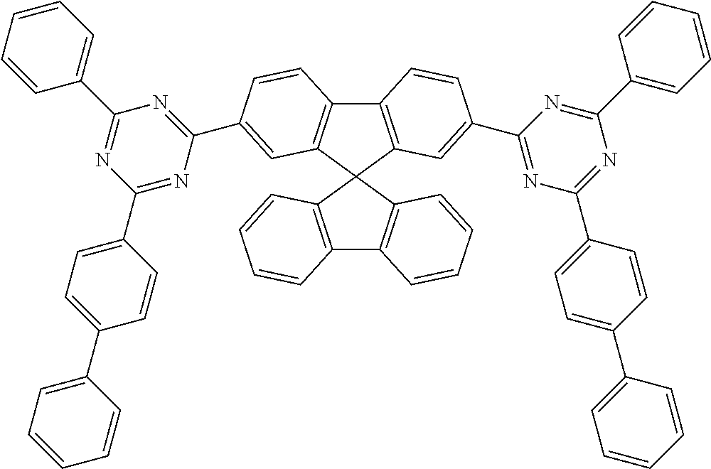 |
62 |
 |
63 |
 |
64 |
 |
65 |
 |
66 |
 |
67 |
 |
68 |
 |
69 |
 |
70 |
 |
71 |
 |
72 |
 |
73 |
 |
74 |
 |
75 |
 |
76 |
 |
77 |
 |
78 |
 |
79 |
 |
80 |
 |
81 |
 |
82 |
 |
83 |
 |
84 |
 |
85 |
 |
86 |
 |
87 |
 |
88 |
 |
89 |
 |
90 |
 |
91 |
 |
92 |
 |
93 |
 |
94 |
 |
95 |
 |
96 |
 |
97 |
 |
98 |
 |
99 |
 |
100 |
 |
101 |
 |
102 |
 |
103 |
 |
104 |
 |
105 |
 |
106 |
 |
107 |
 |
108 |
 |
109 |
 |
110 |
 |
111 |
 |
112 |
 |
113 |
 |
114 |
 |
115 |
 |
116 |
 |
117 |
 |
118 |
 |
119 |
 |
120 |
 |
121 |
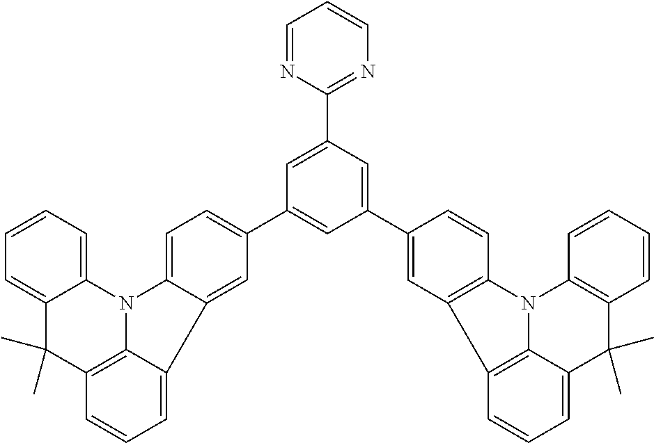 |
122 |
 |
123 |
 |
124 |
 |
125 |
 |
126 |
 |
127 |
 |
128 |
 |
129 |
 |
130 |

where Ar has the meaning given above.


where Ar has the same meaning as described above and furthermore:
- Z is, identically or differently on each occurrence, CR1 or N, where a maximum of 3 symbols Z per ring stand for N; Z is preferably equal to CR1;
- n is, identically or differently on each occurrence, 0 or 1.
- m is, identically or differently on each occurrence, 0, 1, 2 or 3;
- p is, identically or differently on each occurrence, 0 or 1.
- Ar in the above-mentioned formulae preferably stands for an aromatic or heteroaromatic ring system having 5 to 30 aromatic ring atoms which contains no condensed aryl groups having more than 10 aromatic ring atoms, preferably absolutely no condensed aryl groups, and which may be substituted by one or more radicals R1. Particular preference is given to the groups Ar which are mentioned as preferred above. Particular preference is likewise given to the groups R1 which are mentioned as preferred above.


where R1 and n have the meaning given above and the other symbols used have the following meanings:
- Ar3 is on each occurrence, identically or differently, an aromatic ring system having 6 to 60 aromatic C atoms which contains no non-aromatic groups other than carbon or hydrogen; Ar3 here may be substituted by one or more radicals R4;
- R3 is on each occurrence, identically or differently, a straight-chain alkyl group having 1 to 20 C atoms or a branched or cyclic alkyl group having 3 to 20 C atoms, or an aromatic ring system having 6 to 60 aromatic C atoms which contains no non-aromatic groups other than carbon or hydrogen and which may be substituted by one or more radicals R4; two or more radicals R3 here may also form a ring system with one another;
- R4 is on each occurrence, identically or differently, a straight-chain alkyl group having 1 to 20 C atoms or a branched or cyclic alkyl group having 3 to 20 C atoms; two or more radicals R4 here may also form a ring system with one another.


where the symbols used have the meanings given above.


Ar4-Ant-Ar4 formula (41)
where R1 has the meaning given above and the following applies to the other symbols used:
- Ant stands for an anthracene group which is substituted by the groups Ar4 in the 9- and 10-position and which may furthermore be substituted by one or more substituents R1;
- Ar4 is, identically or differently on each occurrence, an aromatic or heteroaromatic ring system having 5 to 60 aromatic ring atoms, which may be substituted by one or more radicals R1.
- 1. The organic electroluminescent device according to the invention has high efficiency. The efficiency here is better than on use of an electron-transport layer which comprises only one of materials ETM1 or ETM2.
- 2. The organic electroluminescent device according to the invention simultaneously has an improved lifetime. The lifetime here is longer than on use of an electron-transport layer which comprises only one of materials ETM1 or ETM2.
- 3. It is not necessary to use a hole-blocking layer as is otherwise usually used in combination with phosphorescent emitter layers. The electroluminescent device according to the invention thus has a simpler structure, which represents a clear advantage. This advantage is evident, in particular, on use of a mixed-host system in the emitting layer, as is frequently used in accordance with the prior art, particularly in the case of phosphorescent emission layers.
- 4. Appropriate mixing ratios of ETM1 and ETM2 enable electron injection and electron transport to be set in such a way that the component is optimised either with respect to the lifetime, the voltage or the efficiency, depending on the desired application.
- 5. Appropriate mixing ratios of ETM1 and ETM2 enable electron injection and electron transport to be set in such a way that, depending on the device architecture (for example top emission or bottom emission) and depending on the emission colour of the device, they may simultaneously also result in a charge balance which is optimum for the component on use of the requisite optical layer thickness of the electron-transport layer.
- 6. Substances which are harmful to health, in particular hydroxyquinoline-metal complexes, can be avoided.
HOMO(eV)=((HEh*27.212)−0.9899)/1.1206
LUMO(eV)=((LEh*27.212)−2.0041)/1.385
| TABLE 1 | ||||
| Ex. No. | ETMX | ETMY | ||
| A1 | ETM1-1(20) | ETM2-1(1) | ||
| A2 | ETM1-1(20) | ETM2-1(2) | ||
| A3 | ETM1-1(20) | ETM2-1(3) | ||
| A4 | ETM1-1(20) | ETM2-1(4) | ||
| A5 | ETM1-1(65%):ETM2-1(35%)(20) | ETM2-1(1.5) | ||
| A6 | ETM1-1(50%):ETM2-1(50%)(20) | ETM2-1(1.5) | ||
| A7 | ETM1-1(35%):ETM2-1(65%)(20) | ETM2-1(1.5) | ||
| A8 | ETM1-1(20%):ETM2-1(80%)(20) | ETM2-1(1.5) | ||
| A9 | ETM1-2(65%):ETM2-1(35%)(20) | ETM2-1(1.5) | ||
| A10 | ETM1-2(50%):ETM2-1(50%)(20) | ETM2-1(1.5) | ||
| A11 | ETM1-2(35%):ETM2-1(65%)(20) | ETM2-1(1.5) | ||
| A12 | ETM1-2(20%):ETM2-1(80%)(20) | ETM2-1(1.5) | ||
| B1 | ETM1-2(65%):ETM2-2(35%)(20) | ETM2-1(1.5) | ||
| B2 | ETM1-2(50%):ETM2-2(50%)(20) | ETM2-1(1.5) | ||
| B3 | ETM1-2(35%):ETM2-2(65%)(20) | ETM2-1(1.5) | ||
| B4 | ETM1-2(20%):ETM2-2(80%)(20) | ETM2-1(1.5) | ||
| A13 | ETM1-1(50%):ETM2-1(50%)(35) | ETM2-1(2) | ||
| A14 | ETM1-1(50%):ETM2-3(50%)(35) | ETM2-1(2) | ||
| A15 | ETM1-3(50%):ETM2-1(50%)(35) | ETM2-1(2) | ||
| B5 | ETM1-3(50%):ETM2-3(50%)(35) | ETM2-1(2) | ||
| B6 | ETM1-3(50%):ETM2-3(50%)(35) | CsF(2) | ||
| B7 | ETM1-3(50%):ETM2-3(50%)(35) | Li3N(0.5) | ||
| B8 | ETM1-3(50%):ETM2-3(50%)(35) | RbF(2) | ||
| B9 | ETM1-3(50%):ETM2-3(50%)(35) | LiF(1.5) | ||
| TABLE 2 |
| Data for the OLEDs |
| CIE y | ||||||
| Ex. | CE1000 | U1000 | CIE x | at | LT | L0 |
| No.: | (cd/A) | (V) | at 1000 cd/m2 | 1000 cd/m2 | (h) | (cd/m2) |
| A1 | 4.05 | 6.10 | 0.140 | 0.154 | 272 | 6000 |
| A2 | 4.31 | 5.86 | 0.140 | 0.156 | 238 | 6000 |
| A3 | 4.33 | 5.82 | 0.140 | 0.156 | 258 | 6000 |
| A4 | 4.39 | 6.20 | 0.141 | 0.152 | 110 | 6000 |
| A5 | 5.04 | 5.47 | 0.142 | 0.162 | 270 | 6000 |
| A6 | 6.13 | 4.99 | 0.142 | 0.159 | 212 | 6000 |
| A7 | 7.04 | 4.76 | 0.142 | 0.158 | 214 | 6000 |
| A8 | 6.49 | 5.25 | 0.142 | 0.159 | 274 | 6000 |
| A9 | 6.68 | 4.05 | 0.142 | 0.159 | 320 | 6000 |
| A10 | 8.12 | 4.13 | 0.141 | 0.159 | 332 | 6000 |
| A11 | 8.24 | 4.02 | 0.142 | 0.161 | 362 | 6000 |
| A12 | 7.36 | 4.68 | 0.142 | 0.159 | 445 | 6000 |
| B1 | 6.97 | 4.15 | 0.142 | 0.155 | 380 | 6000 |
| B2 | 8.50 | 4.06 | 0.142 | 0.154 | 385 | 6000 |
| B3 | 8.64 | 4.11 | 0.142 | 0.156 | 465 | 6000 |
| B4 | 7.45 | 4.27 | 0.142 | 0.156 | 645 | 6000 |
| A13 | 48.01 | 4.00 | 0.356 | 0.605 | 932 | 8000 |
| A14 | 55.82 | 4.19 | 0.349 | 0.608 | 1012 | 8000 |
| A15 | 57.19 | 4.02 | 0.351 | 0.609 | 1053 | 8000 |
| B5 | 68.18 | 3.83 | 0.355 | 0.606 | 1185 | 8000 |
| B6 | 68.30 | 3.81 | 0.354 | 0.607 | 1180 | 8000 |
| B7 | 67.95 | 3.88 | 0.353 | 0.608 | 1175 | 8000 |
| B8 | 67.92 | 3.85 | 0.354 | 0.606 | 1163 | 8000 |
| B9 | 67.86 | 4.57 | 0.356 | 0.605 | 1110 | 8000 |
| TABLE 3 | ||||
| Ex. No. | ETMX | ETMY | ||
| A16 | ETM1-1(50%):ETM2-1(50%)(30) | ETM2-1(1) | ||
| A17 | ETM1-3(50%):ETM2-1(50%)(30) | ETM2-1(1) | ||
| B10 | ETM1-3(50%):ETM2-3(50%)(30) | ETM2-1(1) | ||
| B11 | ETM1-3(50%):ETM2-3(50%)(30) | CsF(1) | ||
| A18 | ETM1-2(50%):ETM2-1(50%)(30) | ETM2-1(1) | ||
| B12 | ETM1-2(50%):ETM2-3(50%)(30) | ETM2-1(1) | ||
| A19 | ETM1-1(50%):ETM2-3(50%)(30) | ETM2-1(1) | ||
| B13 | ETM1-4(50%):ETM2-3(50%)(30) | ETM2-1(1) | ||
| B14 | ETM1-5(50%):ETM2-3(50%)(30) | ETM2-1(1) | ||
| B15 | ETM1-6(50%):ETM2-3(50%)(30) | ETM2-1(1) | ||
| B16 | ETM1-7(50%):ETM2-3(50%)(30) | ETM2-1(1) | ||
| B17 | ETM1-8(50%):ETM2-3(50%)(30) | ETM2-1(1) | ||
| B18 | ETM1-3(50%):ETM2-4(50%)(30) | ETM2-1(1) | ||
| B19 | ETM1-3(50%):ETM2-5(50%)(30) | ETM2-1(1) | ||
| B20 | ETM1-3(50%):ETM2-6(50%)(30) | ETM2-1(1) | ||
| TABLE 4 |
| Data for the OLEDs |
| CIE y | ||||||
| Ex. | CE1000 | U1000 | CIE x | at | LT | L0 |
| No.: | (cd/A) | (V) | at 1000 cd/m2 | 1000 cd/m2 | (h) | (cd/m2) |
| A16 | 49.05 | 3.61 | 0.341 | 0.626 | 1622 | 8000 |
| A17 | 54.00 | 3.49 | 0.342 | 0.624 | 1713 | 8000 |
| B10 | 63.95 | 3.44 | 0.340 | 0.625 | 1928 | 8000 |
| B11 | 63.68 | 3.48 | 0.343 | 0.623 | 1918 | 8000 |
| A18 | 55.50 | 3.42 | 0.341 | 0.625 | 1688 | 8000 |
| B12 | 64.75 | 3.39 | 0.343 | 0.623 | 1907 | 8000 |
| A19 | 51.05 | 3.58 | 0.343 | 0.624 | 1603 | 8000 |
| B13 | 64.24 | 3.49 | 0.342 | 0.622 | 1833 | 8000 |
| B14 | 62.35 | 3.42 | 0.342 | 0.623 | 1783 | 8000 |
| B15 | 64.53 | 3.40 | 0.340 | 0.626 | 1723 | 8000 |
| B16 | 62.86 | 3.51 | 0.344 | 0.621 | 1659 | 8000 |
| B17 | 59.79 | 3.61 | 0.342 | 0.624 | 1678 | 8000 |
| B18 | 61.89 | 3.54 | 0.345 | 0.623 | 1897 | 8000 |
| B19 | 64.91 | 3.41 | 0.342 | 0.626 | 1871 | 8000 |
| B20 | 62.65 | 3.46 | 0.341 | 0.624 | 1843 | 8000 |
| TABLE 5 |
| Structural formulae of the materials used and their function |
| in the OLED |
 |
| HIM1 (HIL) |
 |
| HIM2 (HIL) EP 0676461 |
 |
| HIM3 (HIL) EP 0676461 |
 |
| HIM4 (HIL) WO 2006/122630 |
 |
| HTM1 (HTL), α-NPB |
 |
| HTM2 (HTL) |
 |
| HTM3 (HTL), WO 2012/034627 |
 |
| M1 (host EML), WO 2008/145239 |
 |
| D1 (dopant EML), WO 2008/006449 |
 |
| D2 (dopant EML), WO 2010/012328 |
 |
| M2 (host EML), DE 102009023155 |
 |
| D3 (dopant EML) |
 |
| M3 (host EML), WO 2005/053055 |
 |
| M4 (host EML), WO 2011/088877 |
 |
| ETM1-1 (ETL) |
 |
| ETM2-1 (ETL; EIL), Liq |
 |
| ETM1-2 (ETL), WO 2005/053055 |
 |
| ETM2-2 (ETL), WO 2008/086851 |
 |
| ETM1-3 (ETL), ), WO 2005/053055, DE 10200836982 |
 |
| ETM2-3 (ETL), WO 2009/124627 |
 |
| ETM1-4 (ETL) |
 |
| ETM2-4, E 0676461 |
 |
| ETM1-5 (ETL), WO 2004/093207, WO 2005/054403 |
 |
| ETM2-5 (ETL), DE 102008056688 |
 |
| ETM1-6 (ETL), ), WO 2005/003253, WO 2005/054403 |
 |
| ETM2-6 (ETL), DE 102009023155 |
 |
| ETM1-7 (ETL), TPBI |
 |
| ETM1-8 (ETL) |
| TABLE 6 |
| HOMO/LUMO values and triplet levels T1 |
| of the materials |
| Material | HOMO (eV) | LUMO (eV) | T1 (eV) | Method |
| ETM1-1 | −5.54 | −2.82 | 1.66 | org. |
| ETM2-1 | −4.79 | −2.30 | 1.81 | org. |
| ETM1-2 | −6.05 | −2.79 | 2.70 | org. |
| ETM2-2 | −5.68 | −2.39 | 2.84 | org. |
| ETM1-3 | −6.03 | −2.82 | 2.68 | org. |
| ETM2-3 | −6.16 | −2.24 | 2.95 | org. |
| ETM1-4 | −5.93 | −2.61 | 2.74 | org. |
| ETM2-4 | −5.73 | −2.42 | 2.61 | org. |
| ETM1-5 | −6.04 | −2.81 | 2.57 | org. |
| ETM2-5 | −5.43 | −1.81 | 3.25 | org. |
| ETM1-6 | −5.99 | −2.47 | 2.86 | org. |
| ETM2-6 | −5.54 | −2.27 | 2.82 | org. |
| ETM1-7 | −6.26 | −2.48 | 3.04 | org. |
| ETM1-8 | −6.05 | −2.87 | 2.24 | org. |
Claims (16)
T 1(ETM1)>2.2 eV; and a)
T 1(ETM2)>2.2 eV; and b)
−3.2 eV<LUMO(ETM1)<−2.0 eV; and c)
LUMO(ETM2)>LUMO(ETM1); d)


Priority Applications (1)
| Application Number | Priority Date | Filing Date | Title |
|---|---|---|---|
| US15/645,338 US10636990B2 (en) | 2011-08-22 | 2017-07-10 | Organic electroluminescence device |
Applications Claiming Priority (6)
| Application Number | Priority Date | Filing Date | Title |
|---|---|---|---|
| EP11006859 | 2011-08-22 | ||
| EP11006859 | 2011-08-22 | ||
| EP11006859.0 | 2011-08-22 | ||
| PCT/EP2012/003152 WO2013026515A1 (en) | 2011-08-22 | 2012-07-25 | Organic electroluminescence device |
| US201414240203A | 2014-02-21 | 2014-02-21 | |
| US15/645,338 US10636990B2 (en) | 2011-08-22 | 2017-07-10 | Organic electroluminescence device |
Related Parent Applications (2)
| Application Number | Title | Priority Date | Filing Date |
|---|---|---|---|
| US14/240,203 Division US9735385B2 (en) | 2011-08-22 | 2012-07-25 | Organic electroluminescence device |
| PCT/EP2012/003152 Division WO2013026515A1 (en) | 2011-08-22 | 2012-07-25 | Organic electroluminescence device |
Publications (2)
| Publication Number | Publication Date |
|---|---|
| US20170309855A1 US20170309855A1 (en) | 2017-10-26 |
| US10636990B2 true US10636990B2 (en) | 2020-04-28 |
Family
ID=46581906
Family Applications (2)
| Application Number | Title | Priority Date | Filing Date |
|---|---|---|---|
| US14/240,203 Active 2034-01-20 US9735385B2 (en) | 2011-08-22 | 2012-07-25 | Organic electroluminescence device |
| US15/645,338 Active 2033-03-06 US10636990B2 (en) | 2011-08-22 | 2017-07-10 | Organic electroluminescence device |
Family Applications Before (1)
| Application Number | Title | Priority Date | Filing Date |
|---|---|---|---|
| US14/240,203 Active 2034-01-20 US9735385B2 (en) | 2011-08-22 | 2012-07-25 | Organic electroluminescence device |
Country Status (6)
| Country | Link |
|---|---|
| US (2) | US9735385B2 (en) |
| EP (1) | EP2748878B1 (en) |
| JP (1) | JP6203720B2 (en) |
| KR (2) | KR102051790B1 (en) |
| CN (1) | CN103765623B (en) |
| WO (1) | WO2013026515A1 (en) |
Families Citing this family (25)
| Publication number | Priority date | Publication date | Assignee | Title |
|---|---|---|---|---|
| CN105949177B (en) | 2010-05-03 | 2019-02-01 | 默克专利有限公司 | Preparation and electronic device |
| CN102869672B (en) * | 2010-05-03 | 2016-05-11 | 默克专利有限公司 | Preparation and electronic device |
| DE102010045405A1 (en) * | 2010-09-15 | 2012-03-15 | Merck Patent Gmbh | Materials for organic electroluminescent devices |
| US20160093812A1 (en) * | 2013-04-08 | 2016-03-31 | Merck Patent Gmbh | Organic electroluminescent device |
| KR102188028B1 (en) * | 2013-06-18 | 2020-12-08 | 삼성디스플레이 주식회사 | Organic light emitting device |
| JP2015005747A (en) * | 2013-06-21 | 2015-01-08 | ダウ グローバル テクノロジーズ エルエルシー | Thin film containing compound obtained from triazine, and electronic device formed from the same |
| KR102079254B1 (en) * | 2013-06-24 | 2020-02-20 | 삼성디스플레이 주식회사 | Organic light emitting diode |
| ES2673573T3 (en) * | 2013-12-23 | 2018-06-22 | Novaled Gmbh | Semiconductor material with doping N comprising a phosphine oxide matrix and a doping metal |
| KR101537500B1 (en) * | 2014-04-04 | 2015-07-20 | 주식회사 엘지화학 | Organic light emitting diode |
| EP3663289A1 (en) * | 2014-06-11 | 2020-06-10 | Hodogaya Chemical Co., Ltd. | Pyrimidine derivatives and an organic electroluminescent devices |
| KR102273047B1 (en) * | 2014-06-30 | 2021-07-06 | 삼성디스플레이 주식회사 | Organic light-emitting device |
| EP2963696A1 (en) * | 2014-07-04 | 2016-01-06 | Novaled GmbH | Organic light-emitting diode (OLED) including an electron transport layer stack comprising different lithium compounds |
| US10297762B2 (en) | 2014-07-09 | 2019-05-21 | Universal Display Corporation | Organic electroluminescent materials and devices |
| WO2016068585A1 (en) * | 2014-10-27 | 2016-05-06 | 주식회사 엘지화학 | Organic electroluminescence device |
| KR101745799B1 (en) * | 2014-12-24 | 2017-06-09 | 주식회사 두산 | Organic compound and organic electro luminescence device comprising the same |
| EP3259330B1 (en) * | 2015-02-16 | 2018-11-14 | Merck Patent GmbH | Spirobifluorene derivative-based materials for electronic devices |
| EP3093288A1 (en) * | 2015-05-12 | 2016-11-16 | Novaled GmbH | Organic light-emitting diode comprising different matrix compounds in the first and second electron transport layer |
| EP3147961A1 (en) * | 2015-09-28 | 2017-03-29 | Novaled GmbH | Organic electroluminescent device |
| JP6815294B2 (en) | 2016-09-30 | 2021-01-20 | 株式会社Joled | Organic EL element and organic EL panel |
| US20190355911A1 (en) * | 2016-11-23 | 2019-11-21 | Guangzhou Chinaray Optoelectronic Materials Ltd. | Organic mixture, organic composition, organic electronic component and preparation method therefor |
| KR20190070586A (en) * | 2017-12-13 | 2019-06-21 | 엘지디스플레이 주식회사 | Compound for electron transporting material and organic light emitting diode including the same |
| TWI713848B (en) * | 2018-05-18 | 2020-12-21 | 國立交通大學 | Organic light-emitting device |
| CN110556483A (en) * | 2018-06-04 | 2019-12-10 | Tcl集团股份有限公司 | Electroluminescent device and preparation method and application thereof |
| CN110600623B (en) * | 2018-06-13 | 2021-08-27 | Tcl科技集团股份有限公司 | Electroluminescent device and preparation method thereof |
| US20230059210A1 (en) * | 2018-11-29 | 2023-02-23 | Merck Patent Gmbh | Electronic device |
Citations (9)
| Publication number | Priority date | Publication date | Assignee | Title |
|---|---|---|---|---|
| JP2001237080A (en) | 2000-02-23 | 2001-08-31 | Pioneer Electronic Corp | Organic electroluminescence element |
| US20010052751A1 (en) * | 2000-02-23 | 2001-12-20 | Takeo Wakimoto | Organic electroluminescence element |
| WO2004057926A1 (en) | 2002-12-19 | 2004-07-08 | Semiconductor Energy Laboratory Co., Ltd. | Organic electroluminescent device, light-emitting apparatus using organic electroluminescent device, and electrical appliance using such light-emitting apparatus |
| US20060204784A1 (en) | 2005-03-10 | 2006-09-14 | Begley William J | Organic light-emitting devices with mixed electron transport materials |
| US20060279204A1 (en) | 2005-03-31 | 2006-12-14 | Stephen Forrest | OLEDs utilizing direct injection to the triplet state |
| JP2008078362A (en) | 2006-09-21 | 2008-04-03 | Toray Ind Inc | Light emitting element material and light emitting element |
| US20090072725A1 (en) | 2007-09-13 | 2009-03-19 | Semiconductor Energy Laboratory Co., Ltd. | Light-Emitting Element, Light-Emitting Device, and Electronic Device |
| US20090191427A1 (en) * | 2008-01-30 | 2009-07-30 | Liang-Sheng Liao | Phosphorescent oled having double hole-blocking layers |
| WO2010102706A1 (en) | 2009-03-09 | 2010-09-16 | Merck Patent Gmbh | Organic electroluminescence device |
Family Cites Families (70)
| Publication number | Priority date | Publication date | Assignee | Title |
|---|---|---|---|---|
| US4539507A (en) | 1983-03-25 | 1985-09-03 | Eastman Kodak Company | Organic electroluminescent devices having improved power conversion efficiencies |
| US4780536A (en) | 1986-09-05 | 1988-10-25 | The Ohio State University Research Foundation | Hexaazatriphenylene hexanitrile and its derivatives and their preparations |
| US5061569A (en) | 1990-07-26 | 1991-10-29 | Eastman Kodak Company | Electroluminescent device with organic electroluminescent medium |
| US5151629A (en) | 1991-08-01 | 1992-09-29 | Eastman Kodak Company | Blue emitting internal junction organic electroluminescent device (I) |
| US5837166A (en) | 1993-09-29 | 1998-11-17 | Idemitsu Kosan Co., Ltd. | Organic electroluminescence device and arylenediamine derivative |
| DE69412567T2 (en) | 1993-11-01 | 1999-02-04 | Hodogaya Chemical Co Ltd | Amine compound and electroluminescent device containing it |
| JPH07133483A (en) | 1993-11-09 | 1995-05-23 | Shinko Electric Ind Co Ltd | Organic luminescent material for el element and el element |
| DE59510315D1 (en) | 1994-04-07 | 2002-09-19 | Covion Organic Semiconductors | Spiro compounds and their use as electroluminescent materials |
| DE19652261A1 (en) | 1996-12-16 | 1998-06-18 | Hoechst Ag | Aryl-substituted poly (p-arylenevinylenes), process for their preparation and their use in electroluminescent devices |
| WO1998030071A1 (en) | 1996-12-28 | 1998-07-09 | Tdk Corporation | Organic electroluminescent elements |
| US6097147A (en) * | 1998-09-14 | 2000-08-01 | The Trustees Of Princeton University | Structure for high efficiency electroluminescent device |
| KR100377321B1 (en) | 1999-12-31 | 2003-03-26 | 주식회사 엘지화학 | Electronic device comprising organic compound having p-type semiconducting characteristics |
| JP4220644B2 (en) | 2000-02-14 | 2009-02-04 | 三井化学株式会社 | Amine compound and organic electroluminescent device containing the compound |
| TW532048B (en) | 2000-03-27 | 2003-05-11 | Idemitsu Kosan Co | Organic electroluminescence element |
| US6727644B2 (en) | 2001-08-06 | 2004-04-27 | Eastman Kodak Company | Organic light-emitting device having a color-neutral dopant in an emission layer and in a hole and/or electron transport sublayer |
| ITRM20020411A1 (en) | 2002-08-01 | 2004-02-02 | Univ Roma La Sapienza | SPIROBIFLUORENE DERIVATIVES, THEIR PREPARATION AND USE. |
| KR101030158B1 (en) | 2002-12-23 | 2011-04-18 | 메르크 파텐트 게엠베하 | Organic electroluminescent element |
| CN100479628C (en) * | 2002-12-27 | 2009-04-15 | 富士胶片株式会社 | Organic electroluminescent device |
| DE10310887A1 (en) | 2003-03-11 | 2004-09-30 | Covion Organic Semiconductors Gmbh | Matallkomplexe |
| JP4411851B2 (en) | 2003-03-19 | 2010-02-10 | コニカミノルタホールディングス株式会社 | Organic electroluminescence device |
| EP2281861A3 (en) | 2003-04-15 | 2012-03-28 | Merck Patent GmbH | Mixture of organic emission-enabled semiconductors and matrix materials, use of same and electronic components containing same |
| US7326475B2 (en) | 2003-04-23 | 2008-02-05 | Konica Minolta Holdings, Inc. | Material for organic electroluminescent device, organic electroluminescent device, illuminating device and display |
| EP2251396B1 (en) | 2003-07-07 | 2014-11-19 | Merck Patent GmbH | Organic emission-capable materials and electronic components containing same |
| DE10333232A1 (en) | 2003-07-21 | 2007-10-11 | Merck Patent Gmbh | Organic electroluminescent element |
| US7795801B2 (en) | 2003-09-30 | 2010-09-14 | Konica Minolta Holdings, Inc. | Organic electroluminescent element, illuminator, display and compound |
| DE102004008304A1 (en) | 2004-02-20 | 2005-09-08 | Covion Organic Semiconductors Gmbh | Organic electronic devices |
| US7790890B2 (en) | 2004-03-31 | 2010-09-07 | Konica Minolta Holdings, Inc. | Organic electroluminescence element material, organic electroluminescence element, display device and illumination device |
| KR100787425B1 (en) | 2004-11-29 | 2007-12-26 | 삼성에스디아이 주식회사 | Phenylcarbazole-based compound and Organic electroluminescence display employing the same |
| DE102004023277A1 (en) | 2004-05-11 | 2005-12-01 | Covion Organic Semiconductors Gmbh | New material mixtures for electroluminescence |
| JP4862248B2 (en) | 2004-06-04 | 2012-01-25 | コニカミノルタホールディングス株式会社 | Organic electroluminescence element, lighting device and display device |
| TW200613515A (en) | 2004-06-26 | 2006-05-01 | Merck Patent Gmbh | Compounds for organic electronic devices |
| DE102004031000A1 (en) | 2004-06-26 | 2006-01-12 | Covion Organic Semiconductors Gmbh | Organic electroluminescent devices |
| ITRM20040352A1 (en) | 2004-07-15 | 2004-10-15 | Univ Roma La Sapienza | OLIGOMERIC DERIVATIVES OF SPIROBIFLUORENE, THEIR PREPARATION AND THEIR USE. |
| EP1655359A1 (en) | 2004-11-06 | 2006-05-10 | Covion Organic Semiconductors GmbH | Organic electroluminescent device |
| TW200639140A (en) | 2004-12-01 | 2006-11-16 | Merck Patent Gmbh | Compounds for organic electronic devices |
| KR20100106626A (en) | 2005-01-05 | 2010-10-01 | 이데미쓰 고산 가부시키가이샤 | Aromatic amine derivative and organic electroluminescent device using same |
| JP2006253445A (en) | 2005-03-11 | 2006-09-21 | Toyo Ink Mfg Co Ltd | Organic electroluminescence element |
| EP1860097B1 (en) | 2005-03-18 | 2011-08-10 | Idemitsu Kosan Co., Ltd. | Aromatic amine derivative and organic electroluminescence device utilizing the same |
| JP5242380B2 (en) | 2005-05-03 | 2013-07-24 | メルク パテント ゲーエムベーハー | Organic electroluminescence device |
| DE102005023437A1 (en) | 2005-05-20 | 2006-11-30 | Merck Patent Gmbh | Connections for organic electronic devices |
| US7563518B2 (en) | 2005-07-28 | 2009-07-21 | Eastman Kodak Company | Low voltage organic electroluminescent element |
| JP4593631B2 (en) | 2005-12-01 | 2010-12-08 | 新日鐵化学株式会社 | Compound for organic electroluminescence device and organic electroluminescence device |
| DE102005058543A1 (en) | 2005-12-08 | 2007-06-14 | Merck Patent Gmbh | Organic electroluminescent devices |
| DE102006015183A1 (en) | 2006-04-01 | 2007-10-04 | Merck Patent Gmbh | New benzocycloheptene compound useful in organic electronic devices e.g. organic electroluminescent device, polymer electroluminescent device and organic field-effect-transistors |
| DE102006025777A1 (en) | 2006-05-31 | 2007-12-06 | Merck Patent Gmbh | New materials for organic electroluminescent devices |
| DE102006025846A1 (en) | 2006-06-02 | 2007-12-06 | Merck Patent Gmbh | New materials for organic electroluminescent devices |
| DE102006031990A1 (en) | 2006-07-11 | 2008-01-17 | Merck Patent Gmbh | New materials for organic electroluminescent devices |
| JP4388590B2 (en) | 2006-11-09 | 2009-12-24 | 新日鐵化学株式会社 | Compound for organic electroluminescence device and organic electroluminescence device |
| DE102007002714A1 (en) | 2007-01-18 | 2008-07-31 | Merck Patent Gmbh | New materials for organic electroluminescent devices |
| DE102007024850A1 (en) | 2007-05-29 | 2008-12-04 | Merck Patent Gmbh | New materials for organic electroluminescent devices |
| KR101407580B1 (en) * | 2007-09-17 | 2014-06-13 | 삼성디스플레이 주식회사 | White organic light emitting device and display apparatus and lighting apparatus comprising the same |
| DE102007053771A1 (en) | 2007-11-12 | 2009-05-14 | Merck Patent Gmbh | Organic electroluminescent devices |
| US7862908B2 (en) | 2007-11-26 | 2011-01-04 | National Tsing Hua University | Conjugated compounds containing hydroindoloacridine structural elements, and their use |
| US8221905B2 (en) | 2007-12-28 | 2012-07-17 | Universal Display Corporation | Carbazole-containing materials in phosphorescent light emitting diodes |
| JP5357150B2 (en) | 2008-06-05 | 2013-12-04 | 出光興産株式会社 | Halogen compound, polycyclic compound, and organic electroluminescence device using the same |
| DE102008033943A1 (en) | 2008-07-18 | 2010-01-21 | Merck Patent Gmbh | New materials for organic electroluminescent devices |
| DE102008035413A1 (en) | 2008-07-29 | 2010-02-04 | Merck Patent Gmbh | Connections for organic electronic devices |
| DE102008036982A1 (en) | 2008-08-08 | 2010-02-11 | Merck Patent Gmbh | Organic electroluminescent device |
| KR101506919B1 (en) | 2008-10-31 | 2015-03-30 | 롬엔드하스전자재료코리아유한회사 | Novel compounds for organic electronic material and organic electronic device using the same |
| JP5701766B2 (en) | 2008-11-11 | 2015-04-15 | メルク パテント ゲーエムベーハー | Organic electroluminescent device |
| DE102008056688A1 (en) | 2008-11-11 | 2010-05-12 | Merck Patent Gmbh | Materials for organic electroluminescent devices |
| DE102008064200A1 (en) | 2008-12-22 | 2010-07-01 | Merck Patent Gmbh | Organic electroluminescent device |
| DE102009005746A1 (en) | 2009-01-23 | 2010-07-29 | Merck Patent Gmbh | Materials for organic electroluminescent devices |
| DE102009014513A1 (en) | 2009-03-23 | 2010-09-30 | Merck Patent Gmbh | Organic electroluminescent device |
| DE102009023155A1 (en) | 2009-05-29 | 2010-12-02 | Merck Patent Gmbh | Materials for organic electroluminescent devices |
| DE102009031021A1 (en) | 2009-06-30 | 2011-01-05 | Merck Patent Gmbh | Materials for organic electroluminescent devices |
| DE102009034625A1 (en) | 2009-07-27 | 2011-02-03 | Merck Patent Gmbh | New materials for organic electroluminescent devices |
| DE102009048791A1 (en) | 2009-10-08 | 2011-04-14 | Merck Patent Gmbh | Materials for organic electroluminescent devices |
| DE102009053836A1 (en) | 2009-11-18 | 2011-05-26 | Merck Patent Gmbh | Materials for organic electroluminescent devices |
| DE102010005697A1 (en) | 2010-01-25 | 2011-07-28 | Merck Patent GmbH, 64293 | Connections for electronic devices |
-
2012
- 2012-07-25 CN CN201280040993.4A patent/CN103765623B/en active Active
- 2012-07-25 WO PCT/EP2012/003152 patent/WO2013026515A1/en active Application Filing
- 2012-07-25 EP EP12740070.3A patent/EP2748878B1/en active Active
- 2012-07-25 KR KR1020187031352A patent/KR102051790B1/en active IP Right Grant
- 2012-07-25 US US14/240,203 patent/US9735385B2/en active Active
- 2012-07-25 KR KR1020147007571A patent/KR101914951B1/en active IP Right Grant
- 2012-07-25 JP JP2014526402A patent/JP6203720B2/en active Active
-
2017
- 2017-07-10 US US15/645,338 patent/US10636990B2/en active Active
Patent Citations (18)
| Publication number | Priority date | Publication date | Assignee | Title |
|---|---|---|---|---|
| JP2001237080A (en) | 2000-02-23 | 2001-08-31 | Pioneer Electronic Corp | Organic electroluminescence element |
| US20010043044A1 (en) | 2000-02-23 | 2001-11-22 | Takeo Wakimoto | Organic electroluminescence element |
| US20010052751A1 (en) * | 2000-02-23 | 2001-12-20 | Takeo Wakimoto | Organic electroluminescence element |
| WO2004057926A1 (en) | 2002-12-19 | 2004-07-08 | Semiconductor Energy Laboratory Co., Ltd. | Organic electroluminescent device, light-emitting apparatus using organic electroluminescent device, and electrical appliance using such light-emitting apparatus |
| EP1575339A1 (en) | 2002-12-19 | 2005-09-14 | Semiconductor Energy Laboratory Co., Ltd. | Organic electroluminescent device, light-emitting apparatus using organic electroluminescent device, and electrical appliance using such light-emitting apparatus |
| EP1859491A1 (en) | 2005-03-10 | 2007-11-28 | Eastman Kodak Company | Electroluminescent devices with mixed electron transport materials |
| WO2006098860A1 (en) | 2005-03-10 | 2006-09-21 | Eastman Kodak Company | Electroluminescent devices with mixed electron transport materials |
| US20060204784A1 (en) | 2005-03-10 | 2006-09-14 | Begley William J | Organic light-emitting devices with mixed electron transport materials |
| US20060279204A1 (en) | 2005-03-31 | 2006-12-14 | Stephen Forrest | OLEDs utilizing direct injection to the triplet state |
| JP2008078362A (en) | 2006-09-21 | 2008-04-03 | Toray Ind Inc | Light emitting element material and light emitting element |
| US20090072725A1 (en) | 2007-09-13 | 2009-03-19 | Semiconductor Energy Laboratory Co., Ltd. | Light-Emitting Element, Light-Emitting Device, and Electronic Device |
| US20090191427A1 (en) * | 2008-01-30 | 2009-07-30 | Liang-Sheng Liao | Phosphorescent oled having double hole-blocking layers |
| WO2009097108A1 (en) | 2008-01-30 | 2009-08-06 | Eastman Kodak Company | Phosphorescent oled having double hole-blocking layers |
| KR20100138899A (en) | 2008-01-30 | 2010-12-31 | 글로벌 오엘이디 테크놀러지 엘엘씨 | Phosphorescent oled having double hole-blocking layers |
| JP2011511458A (en) | 2008-01-30 | 2011-04-07 | グローバル・オーエルイーディー・テクノロジー・リミテッド・ライアビリティ・カンパニー | Phosphorescent OLED with double hole blocking layer |
| WO2010102706A1 (en) | 2009-03-09 | 2010-09-16 | Merck Patent Gmbh | Organic electroluminescence device |
| US20110284831A1 (en) | 2009-03-09 | 2011-11-24 | Merck Patent Gmbh | Organic electroluminescence device |
| US20150155514A1 (en) | 2009-03-09 | 2015-06-04 | Merck Patent Gmbh | Organic electroluminescence device |
Non-Patent Citations (1)
| Title |
|---|
| International Search Report for PCT/EP2012/003152 dated Nov. 7, 2012. |
Also Published As
| Publication number | Publication date |
|---|---|
| KR20180121681A (en) | 2018-11-07 |
| CN103765623A (en) | 2014-04-30 |
| JP2014529894A (en) | 2014-11-13 |
| US20170309855A1 (en) | 2017-10-26 |
| WO2013026515A1 (en) | 2013-02-28 |
| EP2748878A1 (en) | 2014-07-02 |
| KR101914951B1 (en) | 2018-11-05 |
| KR102051790B1 (en) | 2019-12-04 |
| KR20140054330A (en) | 2014-05-08 |
| CN103765623B (en) | 2016-06-01 |
| US20140197401A1 (en) | 2014-07-17 |
| US9735385B2 (en) | 2017-08-15 |
| JP6203720B2 (en) | 2017-09-27 |
| EP2748878B1 (en) | 2020-04-01 |
Similar Documents
| Publication | Publication Date | Title |
|---|---|---|
| US10636990B2 (en) | Organic electroluminescence device | |
| US10270052B2 (en) | Electronic device | |
| US9434877B2 (en) | Organic electroluminescent device | |
| US8941297B2 (en) | Organic electroluminescent device | |
| US9385335B2 (en) | Organic electroluminescent device | |
| US9236578B2 (en) | Organic electroluminescent device | |
| US9444064B2 (en) | Organic electroluminescent device | |
| US10249828B2 (en) | Organic electroluminescent device | |
| KR102177883B1 (en) | Organic electroluminescent device | |
| US10069079B2 (en) | Organic electroluminescent device with thermally activated delayed fluorescence material | |
| US9871201B2 (en) | Electronic devices | |
| US20150155514A1 (en) | Organic electroluminescence device | |
| US9066410B2 (en) | Organic electronic device | |
| US9112172B2 (en) | Organic electroluminescence device | |
| KR102253192B1 (en) | Organic electroluminescent device | |
| US9356242B2 (en) | Organic electroluminescent device | |
| US10454040B2 (en) | Materials for electronic devices | |
| US20110108818A1 (en) | Organic electroluminescence device | |
| US20110101328A1 (en) | Organic Electroluminescent Device | |
| US11778907B2 (en) | Composition for organic electronic devices | |
| US11393987B2 (en) | Organic electroluminescent device | |
| US11450809B2 (en) | Composition for organic electronic devices | |
| US20150340636A1 (en) | Electronic Device | |
| US9246118B2 (en) | Organic electroluminescent device |
Legal Events
| Date | Code | Title | Description |
|---|---|---|---|
| AS | Assignment |
Owner name: MERCK PATENT GMBH, GERMANY Free format text: ASSIGNMENT OF ASSIGNORS INTEREST;ASSIGNORS:KROEBER, JONAS VALENTIN;VOGES, FRANK;HEUN, SUSANNE;AND OTHERS;SIGNING DATES FROM 20131106 TO 20131125;REEL/FRAME:042953/0498 |
|
| STPP | Information on status: patent application and granting procedure in general |
Free format text: DOCKETED NEW CASE - READY FOR EXAMINATION |
|
| STPP | Information on status: patent application and granting procedure in general |
Free format text: NON FINAL ACTION MAILED |
|
| STPP | Information on status: patent application and granting procedure in general |
Free format text: RESPONSE TO NON-FINAL OFFICE ACTION ENTERED AND FORWARDED TO EXAMINER |
|
| STPP | Information on status: patent application and granting procedure in general |
Free format text: FINAL REJECTION MAILED |
|
| STPP | Information on status: patent application and granting procedure in general |
Free format text: RESPONSE AFTER FINAL ACTION FORWARDED TO EXAMINER |
|
| STPP | Information on status: patent application and granting procedure in general |
Free format text: NOTICE OF ALLOWANCE MAILED -- APPLICATION RECEIVED IN OFFICE OF PUBLICATIONS |
|
| STCF | Information on status: patent grant |
Free format text: PATENTED CASE |
|
| MAFP | Maintenance fee payment |
Free format text: PAYMENT OF MAINTENANCE FEE, 4TH YEAR, LARGE ENTITY (ORIGINAL EVENT CODE: M1551); ENTITY STATUS OF PATENT OWNER: LARGE ENTITY Year of fee payment: 4 |